JP2024166329A - Display device - Google Patents
Display device Download PDFInfo
- Publication number
- JP2024166329A JP2024166329A JP2024159075A JP2024159075A JP2024166329A JP 2024166329 A JP2024166329 A JP 2024166329A JP 2024159075 A JP2024159075 A JP 2024159075A JP 2024159075 A JP2024159075 A JP 2024159075A JP 2024166329 A JP2024166329 A JP 2024166329A
- Authority
- JP
- Japan
- Prior art keywords
- film
- semiconductor film
- impurity element
- buffer layer
- donor
- Prior art date
- Legal status (The legal status is an assumption and is not a legal conclusion. Google has not performed a legal analysis and makes no representation as to the accuracy of the status listed.)
- Withdrawn
Links
Images


Classifications
-
- H—ELECTRICITY
- H10—SEMICONDUCTOR DEVICES; ELECTRIC SOLID-STATE DEVICES NOT OTHERWISE PROVIDED FOR
- H10D—INORGANIC ELECTRIC SEMICONDUCTOR DEVICES
- H10D1/00—Resistors, capacitors or inductors
- H10D1/40—Resistors
-
- H—ELECTRICITY
- H10—SEMICONDUCTOR DEVICES; ELECTRIC SOLID-STATE DEVICES NOT OTHERWISE PROVIDED FOR
- H10D—INORGANIC ELECTRIC SEMICONDUCTOR DEVICES
- H10D30/00—Field-effect transistors [FET]
- H10D30/01—Manufacture or treatment
- H10D30/021—Manufacture or treatment of FETs having insulated gates [IGFET]
- H10D30/031—Manufacture or treatment of FETs having insulated gates [IGFET] of thin-film transistors [TFT]
- H10D30/0312—Manufacture or treatment of FETs having insulated gates [IGFET] of thin-film transistors [TFT] characterised by the gate electrodes
- H10D30/0316—Manufacture or treatment of FETs having insulated gates [IGFET] of thin-film transistors [TFT] characterised by the gate electrodes of lateral bottom-gate TFTs comprising only a single gate
-
- H—ELECTRICITY
- H10—SEMICONDUCTOR DEVICES; ELECTRIC SOLID-STATE DEVICES NOT OTHERWISE PROVIDED FOR
- H10D—INORGANIC ELECTRIC SEMICONDUCTOR DEVICES
- H10D30/00—Field-effect transistors [FET]
- H10D30/01—Manufacture or treatment
- H10D30/021—Manufacture or treatment of FETs having insulated gates [IGFET]
- H10D30/031—Manufacture or treatment of FETs having insulated gates [IGFET] of thin-film transistors [TFT]
- H10D30/0321—Manufacture or treatment of FETs having insulated gates [IGFET] of thin-film transistors [TFT] comprising silicon, e.g. amorphous silicon or polysilicon
-
- H—ELECTRICITY
- H10—SEMICONDUCTOR DEVICES; ELECTRIC SOLID-STATE DEVICES NOT OTHERWISE PROVIDED FOR
- H10D—INORGANIC ELECTRIC SEMICONDUCTOR DEVICES
- H10D30/00—Field-effect transistors [FET]
- H10D30/60—Insulated-gate field-effect transistors [IGFET]
- H10D30/67—Thin-film transistors [TFT]
- H10D30/6757—Thin-film transistors [TFT] characterised by the structure of the channel, e.g. transverse or longitudinal shape or doping profile
-
- H—ELECTRICITY
- H10—SEMICONDUCTOR DEVICES; ELECTRIC SOLID-STATE DEVICES NOT OTHERWISE PROVIDED FOR
- H10D—INORGANIC ELECTRIC SEMICONDUCTOR DEVICES
- H10D86/00—Integrated devices formed in or on insulating or conducting substrates, e.g. formed in silicon-on-insulator [SOI] substrates or on stainless steel or glass substrates
- H10D86/40—Integrated devices formed in or on insulating or conducting substrates, e.g. formed in silicon-on-insulator [SOI] substrates or on stainless steel or glass substrates characterised by multiple TFTs
- H10D86/421—Integrated devices formed in or on insulating or conducting substrates, e.g. formed in silicon-on-insulator [SOI] substrates or on stainless steel or glass substrates characterised by multiple TFTs having a particular composition, shape or crystalline structure of the active layer
-
- H—ELECTRICITY
- H10—SEMICONDUCTOR DEVICES; ELECTRIC SOLID-STATE DEVICES NOT OTHERWISE PROVIDED FOR
- H10D—INORGANIC ELECTRIC SEMICONDUCTOR DEVICES
- H10D86/00—Integrated devices formed in or on insulating or conducting substrates, e.g. formed in silicon-on-insulator [SOI] substrates or on stainless steel or glass substrates
- H10D86/40—Integrated devices formed in or on insulating or conducting substrates, e.g. formed in silicon-on-insulator [SOI] substrates or on stainless steel or glass substrates characterised by multiple TFTs
- H10D86/441—Interconnections, e.g. scanning lines
-
- H—ELECTRICITY
- H10—SEMICONDUCTOR DEVICES; ELECTRIC SOLID-STATE DEVICES NOT OTHERWISE PROVIDED FOR
- H10D—INORGANIC ELECTRIC SEMICONDUCTOR DEVICES
- H10D86/00—Integrated devices formed in or on insulating or conducting substrates, e.g. formed in silicon-on-insulator [SOI] substrates or on stainless steel or glass substrates
- H10D86/40—Integrated devices formed in or on insulating or conducting substrates, e.g. formed in silicon-on-insulator [SOI] substrates or on stainless steel or glass substrates characterised by multiple TFTs
- H10D86/60—Integrated devices formed in or on insulating or conducting substrates, e.g. formed in silicon-on-insulator [SOI] substrates or on stainless steel or glass substrates characterised by multiple TFTs wherein the TFTs are in active matrices
-
- H—ELECTRICITY
- H10—SEMICONDUCTOR DEVICES; ELECTRIC SOLID-STATE DEVICES NOT OTHERWISE PROVIDED FOR
- H10D—INORGANIC ELECTRIC SEMICONDUCTOR DEVICES
- H10D30/00—Field-effect transistors [FET]
- H10D30/60—Insulated-gate field-effect transistors [IGFET]
- H10D30/67—Thin-film transistors [TFT]
- H10D30/6729—Thin-film transistors [TFT] characterised by the electrodes
- H10D30/6737—Thin-film transistors [TFT] characterised by the electrodes characterised by the electrode materials
- H10D30/6739—Conductor-insulator-semiconductor electrodes
-
- H—ELECTRICITY
- H10—SEMICONDUCTOR DEVICES; ELECTRIC SOLID-STATE DEVICES NOT OTHERWISE PROVIDED FOR
- H10D—INORGANIC ELECTRIC SEMICONDUCTOR DEVICES
- H10D30/00—Field-effect transistors [FET]
- H10D30/60—Insulated-gate field-effect transistors [IGFET]
- H10D30/67—Thin-film transistors [TFT]
- H10D30/674—Thin-film transistors [TFT] characterised by the active materials
- H10D30/6741—Group IV materials, e.g. germanium or silicon carbide
- H10D30/6743—Silicon
-
- H—ELECTRICITY
- H10—SEMICONDUCTOR DEVICES; ELECTRIC SOLID-STATE DEVICES NOT OTHERWISE PROVIDED FOR
- H10D—INORGANIC ELECTRIC SEMICONDUCTOR DEVICES
- H10D62/00—Semiconductor bodies, or regions thereof, of devices having potential barriers
- H10D62/40—Crystalline structures
Landscapes
- Thin Film Transistor (AREA)
- Liquid Crystal (AREA)
- Electroluminescent Light Sources (AREA)
- Metal-Oxide And Bipolar Metal-Oxide Semiconductor Integrated Circuits (AREA)
- Semiconductor Integrated Circuits (AREA)
- Devices For Indicating Variable Information By Combining Individual Elements (AREA)
- Electrodes Of Semiconductors (AREA)
Abstract
Description
本発明は、ダイオード、及びそれを有する表示装置に関する。 The present invention relates to a diode and a display device having the same.
近年、絶縁表面を有する基板上に形成された半導体薄膜(厚さ数十~数百nm程度)を用
いて薄膜トランジスタを構成する技術が注目されている。薄膜トランジスタはICや電気
光学装置のような電子デバイスに広く応用され、特に画像表示装置のスイッチング素子と
して開発が急がれている。
In recent years, attention has been focused on a technology for constructing thin-film transistors using a semiconductor thin film (with a thickness of about tens to hundreds of nm) formed on a substrate with an insulating surface. Thin-film transistors are widely used in electronic devices such as ICs and electro-optical devices, and their development as switching elements in image display devices is particularly urgent.
画像表示装置のスイッチング素子として、非晶質半導体膜を用いた薄膜トランジスタ、結
晶粒径が100nm以上の多結晶半導体膜を用いた薄膜トランジスタ等が用いられている
。多結晶半導体膜の形成方法としては、パルス発振のエキシマレーザビームを光学系によ
り線状に加工して、非晶質珪素膜に対し線状ビームを走査させながら照射して結晶化する
技術が知られている。
As switching elements of image display devices, thin film transistors using amorphous semiconductor films, thin film transistors using polycrystalline semiconductor films with crystal grain sizes of 100 nm or more, etc. As a method for forming a polycrystalline semiconductor film, a technique is known in which a pulsed excimer laser beam is processed into a linear shape by an optical system, and an amorphous silicon film is irradiated with the linear beam while being scanned thereon to crystallize the film.
また、画像表示装置のスイッチング素子として、結晶粒径が1nm~100nm程度の微
結晶半導体膜を用いた薄膜トランジスタが用いられている(特許文献1及び2)。
Furthermore, thin film transistors using a microcrystalline semiconductor film with a crystal grain size of about 1 nm to 100 nm are used as switching elements of image display devices (Patent Documents 1 and 2).
多結晶半導体膜を用いた薄膜トランジスタは、非晶質半導体膜を用いた薄膜トランジスタ
に比べて電界効果移動度が2桁以上高く、半導体表示装置の画素部とその周辺の駆動回路
を同一基板上に一体形成できるという利点を有している。しかしながら、非晶質半導体膜
を用いた場合に比べて、半導体膜の結晶化のために工程が複雑化するため、その分歩留ま
りが低減し、コストが高まるという問題がある。
A thin film transistor using a polycrystalline semiconductor film has an advantage that the field effect mobility is two or more orders of magnitude higher than that of a thin film transistor using an amorphous semiconductor film, and the pixel portion of a semiconductor display device and its surrounding driving circuit can be integrally formed on the same substrate. However, compared to the case where an amorphous semiconductor film is used, the process becomes more complicated due to crystallization of the semiconductor film, which leads to a problem that the yield is reduced and the cost is increased.
また、微結晶半導体膜をチャネル形成領域に用いた逆スタガ型の薄膜トランジスタは、非
晶質半導体膜をチャネル形成領域に用いた逆スタガ型の薄膜トランジスタと比較して、オ
ン電流を向上させることが可能であるが、それと共に、オフ電流も上昇してしまう。オフ
電流の高い薄膜トランジスタを用いた表示装置は、コントラストが低下すると共に、消費
電力も高くなるという問題がある。
In addition, an inverted staggered thin film transistor using a microcrystalline semiconductor film for a channel formation region can have a higher on-current than an inverted staggered thin film transistor using an amorphous semiconductor film for a channel formation region, but the off-current also increases. A display device using a thin film transistor with a high off-current has a problem of lowering contrast and increasing power consumption.
上述した問題に鑑み、本発明は、薄膜トランジスタのオフ電流を低減することを目的の一
とする。また、ダイオードの逆方向電流を低減することを目的の一とする。また、表示装
置の画質の向上を目的の一とする。
In view of the above problems, an object of the present invention is to reduce the off-current of a thin film transistor, to reduce the reverse current of a diode, and to improve the image quality of a display device.
本発明の一は、ゲート電極上に、ゲート絶縁膜を介して該ゲート電極の端部に至らない内
側領域に設けられた微結晶半導体膜と、微結晶半導体膜の上面及び側面を被覆する非晶質
半導体膜と、非晶質半導体膜上に、ソース領域及びドレイン領域をそれぞれ形成する一導
電型の不純物元素が添加された不純物半導体膜と、を有し、微結晶半導体膜は、ドナーと
なる不純物元素を含むことを特徴とする薄膜トランジスタである。
One aspect of the present invention is a thin film transistor including: a microcrystalline semiconductor film provided over a gate electrode in an inner region not reaching an end of the gate electrode with a gate insulating film therebetween; an amorphous semiconductor film covering an upper surface and a side surface of the microcrystalline semiconductor film; and an impurity semiconductor film to which an impurity element of one conductivity type is added and which forms a source region and a drain region, respectively, over the amorphous semiconductor film, wherein the microcrystalline semiconductor film contains an impurity element which serves as a donor.
微結晶半導体膜のソース領域及びドレイン領域側の端部は、非晶質半導体膜、不純物半導
体膜と重なっていてもよい。また、微結晶半導体膜の端部の一部がソース電極またはドレ
イン電極に覆われていてもよい。また、非晶質半導体膜の端部は、ソース電極及びドレイ
ン電極の外側に露出していてもよい。
Ends of the microcrystalline semiconductor film on the source and drain region sides may overlap with the amorphous semiconductor film and the impurity semiconductor film. Further, a part of the end of the microcrystalline semiconductor film may be covered with the source electrode or the drain electrode. Further, the end of the amorphous semiconductor film may be exposed to the outside of the source electrode and the drain electrode.
本発明の一は、ゲート電極上に、ゲート絶縁膜を介して該ゲート電極の端部に至らない内
側領域に設けられ、且つドナーとなる不純物元素が添加された微結晶半導体膜と、微結晶
半導体膜の上面及び側面を被覆する非晶質半導体膜と、非晶質半導体膜上に、ソース領域
またはドレイン領域を形成する一導電型の不純物元素が添加された不純物半導体膜と、不
純物半導体膜に接する配線と、コモン線と、を有し、ゲート電極及び配線は導電膜で接続
されるダイオードである。
One aspect of the present invention is a diode including: a microcrystalline semiconductor film provided over a gate electrode in an inner region not reaching an end of the gate electrode with a gate insulating film therebetween and doped with an impurity element serving as a donor; an amorphous semiconductor film covering an upper surface and side surfaces of the microcrystalline semiconductor film; an impurity semiconductor film doped with an impurity element of one conductivity type forming a source region or a drain region over the amorphous semiconductor film; a wiring in contact with the impurity semiconductor film; and a common line, in which the gate electrode and the wiring are connected through a conductive film.
本発明の一は、ゲート電極上に、ゲート絶縁膜を介して該ゲート電極の端部に至らない内
側領域に設けられ、且つドナーとなる不純物元素が添加された微結晶半導体膜と、微結晶
半導体膜の上面及び側面を被覆する非晶質半導体膜と、非晶質半導体膜上に、ソース領域
またはドレイン領域を形成する一導電型の不純物元素が添加された不純物半導体膜と、不
純物半導体膜に接する配線と、コモン線と、を有し、ゲート電極及び配線は第1の導電膜
で接続され、非晶質半導体膜または微結晶半導体膜とコモン線とが第2の導電膜で接続さ
れるダイオードである。
One aspect of the present invention is a diode including: a microcrystalline semiconductor film provided over a gate electrode in an inner region not reaching an end of the gate electrode with a gate insulating film therebetween and to which an impurity element serving as a donor is added; an amorphous semiconductor film covering an upper surface and side surfaces of the microcrystalline semiconductor film; an impurity semiconductor film to which an impurity element of one conductivity type is added and which forms a source region or a drain region on the amorphous semiconductor film; a wiring in contact with the impurity semiconductor film; and a common line, in which the gate electrode and the wiring are connected by a first conductive film, and the amorphous semiconductor film or the microcrystalline semiconductor film and the common line are connected by a second conductive film.
なお、微結晶半導体膜のソース領域またはドレイン領域側の端部は、非晶質半導体膜、不
純物半導体膜と重なっていてもよい。また、非晶質半導体膜の端部の一部がソース電極ま
たはドレイン電極に覆われていてもよい。また、非晶質半導体膜の端部は、ソース電極及
びドレイン電極の外側に露出していてもよい。
Note that an end portion of the microcrystalline semiconductor film on the source region or drain region side may overlap with the amorphous semiconductor film or the impurity semiconductor film. A part of the end portion of the amorphous semiconductor film may be covered with the source electrode or the drain electrode. The end portion of the amorphous semiconductor film may be exposed to the outside of the source electrode and the drain electrode.
本発明において、微結晶半導体膜に重ねて非晶質半導体膜が設けられていてもよい。 In the present invention, an amorphous semiconductor film may be provided over the microcrystalline semiconductor film.
また、本発明において、微結晶半導体膜は、微結晶シリコン膜、微結晶ゲルマニウム膜、
または微結晶シリコンゲルマニウム膜であってもよい。また、微結晶半導体膜は、微結晶
シリコン膜及び微結晶ゲルマニウム膜の積層構造であってもよい。また、微結晶半導体膜
は、ドナーとなる不純物元素が添加された結晶粒と、結晶粒を覆うゲルマニウム膜であっ
てもよい。また、微結晶半導体膜の代わりに、非晶質ゲルマニウム膜、または非晶質シリ
コンゲルマニウム膜を用いてもよい。
In the present invention, the microcrystalline semiconductor film may be a microcrystalline silicon film, a microcrystalline germanium film,
Alternatively, the microcrystalline semiconductor film may be a microcrystalline silicon germanium film. The microcrystalline semiconductor film may have a stacked structure of a microcrystalline silicon film and a microcrystalline germanium film. The microcrystalline semiconductor film may be a crystal grain to which an impurity element serving as a donor is added, and a germanium film covering the crystal grain. Instead of the microcrystalline semiconductor film, an amorphous germanium film or an amorphous silicon germanium film may be used.
また、ドナーとなる不純物元素は、リン、砒素、またはアンチモンである。 The donor impurity element is phosphorus, arsenic, or antimony.
また、微結晶半導体膜をチャネル形成領域に用いた薄膜トランジスタ(TFT)を画素部
、さらには駆動回路に用いて表示装置を作製する。本発明の微結晶半導体膜は、ゲート絶
縁膜との界面における結晶性が高いため、当該微結晶半導体膜を用いた薄膜トランジスタ
は、その電界効果移動度が2.5~10cm2/V・secと、非晶質半導体膜を用いた
薄膜トランジスタの5~20倍の電界効果移動度を有しているので、駆動回路の一部また
は全体を、画素部と同じ基板上に一体形成し、システムオンパネルを形成することができ
る。
A display device is manufactured by using a thin film transistor (TFT) using a microcrystalline semiconductor film in a channel formation region in a pixel portion and further in a driver circuit. Since the microcrystalline semiconductor film of the present invention has high crystallinity at the interface with a gate insulating film, a thin film transistor using the microcrystalline semiconductor film has a field effect mobility of 2.5 to 10 cm 2 /V·sec, which is 5 to 20 times that of a thin film transistor using an amorphous semiconductor film. Therefore, a part or the whole of the driver circuit can be integrally formed over the same substrate as the pixel portion to form a system-on-panel.
また、表示装置としては、発光装置や液晶表示装置を含む。発光装置は発光素子を含み、
液晶表示装置は液晶素子を含む。発光素子は、電流または電圧によって輝度が制御される
素子をその範疇に含んでおり、具体的には有機EL(エレクトロルミネッセンス)及び無
機ELが含まれる。
The display device includes a light-emitting device and a liquid crystal display device. A light-emitting device includes a light-emitting element,
The liquid crystal display device includes a liquid crystal element. The light-emitting element includes an element whose luminance is controlled by a current or a voltage, and specifically includes an organic electroluminescence (EL) element and an inorganic EL element.
また、表示装置は、表示素子が封止された状態にあるパネルと、該パネルにコントローラ
を含むIC等を実装した状態にあるモジュールとを含む。さらに本発明の一は、該表示装
置を作製する過程における、表示素子が完成する前の一形態に相当する素子基板に関し、
該素子基板は、電流を表示素子に供給するための手段を複数の各画素に備える。素子基板
は、具体的には、表示素子の画素電極のみが形成された状態であっても良いし、画素電極
となる導電膜を成膜した後であって、エッチングして画素電極を形成する前の状態であっ
ても良いし、あらゆる形態があてはまる。
The display device includes a panel in which a display element is sealed, and a module in which an IC including a controller is mounted on the panel. Another aspect of the present invention relates to an element substrate that corresponds to one form before the display element is completed in the process of manufacturing the display device,
The element substrate includes a means for supplying a current to each of the plurality of pixels. Specifically, the element substrate may be in a state where only pixel electrodes of the display elements are formed, or in a state where a conductive film that becomes the pixel electrodes is formed but not yet etched to form the pixel electrodes, or in any other form.
なお、本明細書中における表示装置とは、画像表示デバイス、発光デバイス、もしくは光
源(照明装置含む)を指す。また、コネクター、例えばFPC(Flexible pr
inted circuit)もしくはTAB(Tape Automated Bon
ding)テープもしくはTCP(Tape Carrier Package)が取り
付けられたモジュール、TABテープやTCPの先にプリント配線板が設けられたモジュ
ール、または表示素子にCOG(Chip On Glass)方式によりIC(集積回
路)が直接実装されたモジュールも全て表示装置に含むものとする。
In this specification, the term "display device" refers to an image display device, a light emitting device, or a light source (including a lighting device).
integrated circuit) or TAB (Tape Automated Bon
The term "display device" also includes modules to which TAB tape or TCP (Tape Carrier Package) is attached, modules in which a printed wiring board is provided at the end of TAB tape or TCP, and modules in which an IC (integrated circuit) is directly mounted on a display element by a COG (chip on glass) method.
本発明により、薄膜トランジスタのオフ電流を低減することができる。また、オン電流及
び電界効果移動度が高く、また、オフ電流を低減した薄膜トランジスタを作製することが
できる。また、ダイオードの逆方向電流を低減することができる。また、高電圧印加時の
スイッチング速度の速いダイオードを作製することができる。このため、表示装置の画質
を向上させることができる。
According to the present invention, the off-current of a thin film transistor can be reduced. In addition, a thin film transistor having high on-current and high field effect mobility and reduced off-current can be manufactured. In addition, the reverse current of a diode can be reduced. In addition, a diode having a high switching speed when a high voltage is applied can be manufactured. As a result, the image quality of a display device can be improved.
本発明の実施の形態について、図面を用いて以下に説明する。但し、本発明は以下の説明
に限定されず、本発明の趣旨及びその範囲から逸脱することなくその形態及び詳細をさま
ざまに変更し得ることは当業者であれば容易に理解される。従って、本発明は以下に示す
実施の形態の記載内容に限定して解釈されるものではない。以下に説明する本発明の構成
において、同じものを指す符号は異なる図面間で共通して用いる。
The following describes the embodiments of the present invention with reference to the drawings. However, the present invention is not limited to the following description, and it is easily understood by those skilled in the art that the form and details of the present invention can be modified in various ways without departing from the spirit and scope of the present invention. Therefore, the present invention should not be interpreted as being limited to the description of the embodiments shown below. In the configuration of the present invention described below, the same reference numerals are used in common between different drawings to indicate the same parts.
(実施の形態1)
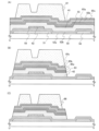
本実施の形態では、移動度及びオン電流が高く、且つオフ電流の低い薄膜トランジスタの
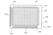
作製工程について、以下に示す。本実施の形態では、図14に示す表示装置の素子基板1
300の上面図において、画素部1331の各画素に形成される薄膜トランジスタ、画素
電極、及び容量素子の作製工程を以下に示す。
(Embodiment 1)
In this embodiment mode, a manufacturing process of a thin film transistor having high mobility, high on-state current, and low off-state current will be described below. In this embodiment mode, an element substrate 1 of a display device shown in FIG.
In the top view of 300, a manufacturing process of a thin film transistor, a pixel electrode, and a capacitor element formed in each pixel of the
図14の画素部1331の一画素の薄膜トランジスタ及び画素電極が接続する領域の拡大
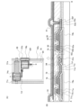
図を図5に示し、図5のQ-Rの断面図を図1乃至図3に示し、S-Tの断面図を図4に
示す。
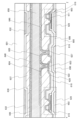
FIG. 5 shows an enlarged view of a region where a thin film transistor and a pixel electrode of one pixel of the
図1(A)に示すように、基板50上にゲート電極51、容量配線56を形成し、ゲート
電極51、容量配線56上に、ゲート絶縁膜52a、52bを形成する。
As shown in FIG. 1A, a
基板50は、バリウムホウケイ酸ガラス、アルミノホウケイ酸ガラス、若しくはアルミノ
シリケートガラスなど、フュージョン法やフロート法で作製される無アルカリガラス基板
、セラミック基板の他、本作製工程の処理温度に耐えうる耐熱性を有するプラスチック基
板等を用いることができる。また、ステンレス合金などの金属基板の表面に絶縁膜を設け
た基板を適用しても良い。
The
ゲート電極51、容量配線56は、スパッタリング法、CVD法、めっき法、印刷法、液
滴吐出法等を用いて形成する。ここでは、基板50上に導電膜としてモリブデン膜をスパ
ッタリング法により成膜し、第1のフォトマスクを用いて形成したレジストマスクを用い
て基板50上に形成された導電膜をエッチングしてゲート電極51、容量配線56を形成
する。
The
ゲート電極51は、金属材料で形成される。金属材料としてはアルミニウム、クロム、チ
タン、タンタル、モリブデン、銅などが適用される。ゲート電極51の好適例は、アルミ
ニウム又はアルミニウムとバリア金属の積層構造体によって形成される。バリア金属とし
ては、チタン、モリブデン、クロムなどの高融点金属が適用される。バリア金属はアルミ
ニウムのヒロック防止、酸化防止のために設けることが好ましい。
The
ゲート電極51は厚さ50nm以上300nm以下で形成する。ゲート電極51の厚さを
50nm以上100nm以下とすることで、後に形成される微結晶ゲルマニウム膜や配線
の段切れ防止が可能である。また、ゲート電極51の厚さを150nm以上300nm以
下とすることで、ゲート電極51の抵抗率を低減することが可能であり、大面積化が可能
である。
The
なお、ゲート電極51上には微結晶半導体膜や配線を形成するので、段切れ防止のため端
部がテーパー状になるように加工することが望ましい。また、図示しないがこの工程でゲ
ート電極に接続する配線、容量配線、コモン線等も同時に形成することができる。
In addition, since a microcrystalline semiconductor film and wiring are formed on the
ゲート絶縁膜52a、52bはそれぞれ、CVD法やスパッタリング法等を用いて、厚さ
50~150nmの酸化珪素膜、窒化珪素膜、酸化窒化珪素膜、または窒化酸化珪素膜で
形成することができる。ここでは、ゲート絶縁膜52aとして窒化珪素膜または窒化酸化
珪素膜を形成し、ゲート絶縁膜52bとして酸化珪素膜または酸化窒化珪素膜を形成して
積層する形態を示す。なお、ゲート絶縁膜を2層とせず、ゲート絶縁膜を、酸化珪素膜、
窒化珪素膜、酸化窒化珪素膜、または窒化酸化珪素膜の単層で形成することができる。ま
た、ゲート絶縁膜を、上記絶縁膜を用いて3層構造とすることができる。
The
The gate insulating film can be formed of a single layer of a silicon nitride film, a silicon oxynitride film, or a silicon nitride oxide film. The gate insulating film can also have a three-layer structure using the above insulating films.
ゲート絶縁膜52aを窒化珪素膜、または窒化酸化珪素膜を用いて形成することで、基板
50とゲート絶縁膜52aの密着力が高まり、基板50としてガラス基板を用いた場合、
基板50からの不純物が微結晶半導体膜に拡散するのを防止することが可能であり、さら
にゲート電極51の酸化防止が可能である。即ち、膜剥れを防止することができると共に
、後に形成される薄膜トランジスタの電気特性を向上させることができる。また、ゲート
絶縁膜52a、52bはそれぞれ厚さ50nm以上であると、ゲート電極51の凹凸によ
る被覆率の低減を緩和することが可能であるため好ましい。
By forming the
It is possible to prevent impurities from the
ここでは、酸化窒化珪素膜とは、その組成として、窒素よりも酸素の含有量が多いもので
あって、ラザフォード後方散乱法(RBS:Rutherford Backscatt
ering Spectrometry)及び水素前方散乱法(HFS:Hydroge
n Forward Scattering)を用いて測定した場合に、組成範囲として
酸素が50~70原子%、窒素が0.5~15原子%、シリコンが25~35原子%、水
素が0.1~10原子%の範囲で含まれるものをいう。また、窒化酸化珪素膜とは、その
組成として、酸素よりも窒素の含有量が多いものであって、RBS及びHFSを用いて測
定した場合に、組成範囲として酸素が5~30原子%、窒素が20~55原子%、シリコ
ンが25~35原子%、水素が10~30原子%の範囲で含まれるものをいう。但し、酸
化窒化シリコンまたは窒化酸化シリコンを構成する原子の合計を100原子%としたとき
、窒素、酸素、シリコン及び水素の含有比率が上記の範囲内に含まれるものとする。
Here, the silicon oxynitride film is a film having a composition in which the oxygen content is greater than that of nitrogen, and is measured by Rutherford Backscattering Spectroscopy (RBS).
ering spectrometry) and Hydrogen Forward Scattering (HFS)
n Forward Scattering), the composition ranges are 50 to 70 atomic % oxygen, 0.5 to 15 atomic % nitrogen, 25 to 35 atomic % silicon, and 0.1 to 10 atomic % hydrogen. The silicon nitride oxide film refers to a film whose composition contains more nitrogen than oxygen, and whose composition ranges are 5 to 30 atomic % oxygen, 20 to 55 atomic % nitrogen, 25 to 35 atomic % silicon, and 10 to 30 atomic % hydrogen, when measured using RBS and HFS. However, when the total of the atoms constituting silicon oxynitride or silicon nitride oxide is taken as 100 atomic %, the content ratios of nitrogen, oxygen, silicon, and hydrogen are within the above ranges.
次に、ゲート絶縁膜52b上に、ドナーとなる不純物元素を含む微結晶半導体膜45を形
成する。ドナーとなる不純物元素を含む微結晶半導体膜58としては、リン、砒素、アン
チモン等のドナーとなる不純物元素を含む、微結晶シリコン膜、微結晶ゲルマニウム膜、
微結晶シリコンゲルマニウム等がある。
Next, a
Examples include microcrystalline silicon germanium.
ここでの微結晶半導体膜とは、非晶質と結晶構造(単結晶、多結晶を含む)の中間的な構
造の半導体を含む膜である。この半導体は、自由エネルギー的に安定な第3の状態を有す
る半導体であって、短距離秩序を持ち格子歪みを有する結晶質なものであり、粒径が0.
5~20nmの柱状または針状結晶が基板表面に対して法線方向に成長している。また、
複数の微結晶半導体の間に非単結晶半導体が存在している。微結晶半導体の代表例である
微結晶シリコンは、そのラマンスペクトルが単結晶シリコンを示す520cm-1よりも
低波数側に、シフトしている。即ち、単結晶シリコンを示す520cm-1とアモルファ
スシリコンを示す480cm-1の間に微結晶シリコンのラマンスペクトルのピークがあ
る。また、未結合手(ダングリングボンド)を終端するため水素またはハロゲンを少なく
とも1原子%またはそれ以上含ませている。さらに、ヘリウム、アルゴン、クリプトン、
ネオンなどの希ガス元素を含ませて格子歪みをさらに助長させることで、安定性が増し良
好な微結晶半導体膜が得られる。このような微結晶半導体膜に関する記述は、例えば、米
国特許4,409,134号で開示されている。
The microcrystalline semiconductor film here is a film containing a semiconductor having an intermediate structure between an amorphous structure and a crystalline structure (including single crystal and polycrystalline). This semiconductor is a semiconductor having a third state that is stable in terms of free energy, and is crystalline with a short-range order and lattice distortion, and has a grain size of 0.
Columnar or needle-like crystals of 5 to 20 nm are grown in the normal direction to the substrate surface.
A non-single crystal semiconductor is present between a plurality of microcrystalline semiconductors. The Raman spectrum of microcrystalline silicon, which is a typical example of a microcrystalline semiconductor, is shifted to the lower wave number side from 520 cm −1 which indicates single crystal silicon. That is, the peak of the Raman spectrum of microcrystalline silicon is between 520 cm −1 which indicates single crystal silicon and 480 cm −1 which indicates amorphous silicon. In addition, at least 1 atomic % or more of hydrogen or halogen is contained in order to terminate dangling bonds. Furthermore, helium, argon, krypton,
By adding a rare gas element such as neon to further promote lattice distortion, a good microcrystalline semiconductor film with increased stability can be obtained. Such a microcrystalline semiconductor film is disclosed in, for example, U.S. Pat. No. 4,409,134.
ドナーとなる不純物元素を含む微結晶半導体膜58の厚さは、1nm以上200nm以下
、好ましくは1nm以上100nm以下、好ましくは1nm以上50nm以下、好ましく
は10nm以上25nm以下で形成する。ドナーとなる不純物元素を含む微結晶半導体膜
58の厚さを1nm以上50nm以下とすることで、完全空乏型の薄膜トランジスタを作
製することができる。
The thickness of the
微結晶半導体膜に含まれるドナーとなる不純物元素の濃度は、6×1015cm-3以上
3×1018cm-3以下、好ましくは1×1016cm-3以上3×1018cm-3
以下、好ましくは3×1016cm-3以上3×1017cm-3以下とする。微結晶半
導体膜58に含まれるドナーとなる不純物元素の濃度を上記範囲とすることにより、ゲー
ト絶縁膜52b及び微結晶半導体膜58の界面における結晶性を高めることが可能であり
、微結晶半導体膜58の抵抗率を低減することが可能であるため、電界効果移動度が高く
、オン電流の高い薄膜トランジスタを作製することができる。なお、微結晶半導体膜に含
まれるドナーとなる不純物元素のピーク濃度を6×1015cm-3未満とすると、ドナ
ーとなる不純物元素の量が不十分で、電界効果移動度、及びオン電流の上昇が望めない。
また、微結晶半導体膜に含まれるドナーとなる不純物元素のピーク濃度を3×10¹⁸c
m-3より大とすると、閾値電圧がゲート電圧のマイナス側にシフトしてしまい、薄膜ト
ランジスタとしての動作をしないため、ドナーとなる不純物元素の濃度は、6×10¹⁵
cm-3以上3×1018cm-3以下、好ましくは1×1016cm-3以上3×10
18cm-3以下、好ましくは3×1016cm-3以上3×1017cm-3以下であ
ることが好ましい。
The concentration of an impurity element serving as a donor contained in the microcrystalline semiconductor film is greater than or equal to 6×10 15 cm −3 and less than or equal to 3×10 18 cm −3 , preferably greater than or equal to 1×10 16 cm −3 and less than or equal to 3×10 18 cm −3 .
The concentration of the impurity element serving as a donor contained in the
In addition, the peak concentration of the impurity element serving as a donor contained in the microcrystalline semiconductor film is set to 3×10 18 c
If the concentration of the impurity element acting as a donor is greater than 6× 10 −3 , the threshold voltage is shifted to the negative side of the gate voltage, and the thin film transistor does not function.
cm -3 or more and 3×10 18 cm -3 or less, preferably 1×10 16 cm -3 or more and 3×10
18 cm -3 or less, and preferably from 3 x 10 16 cm -3 to 3 x 10 17 cm -3 .
また、ドナーとなる不純物元素を含む微結晶半導体膜58の酸素濃度、及び窒素濃度は、
ドナーとなる不純物元素の濃度の10倍未満、代表的には3×10¹⁹atoms/cm
3未満、更に好ましくは3×10¹⁸atoms/cm3未満、炭素の濃度を3×101
8atoms/cm3以下とすることが好ましい。酸素、窒素、及び炭素が微結晶半導体
膜に混入する濃度を低減することで、ドナーとなる不純物元素を含む微結晶半導体膜58
の欠陥の生成を抑制する事ができる。さらには、酸素、または窒素が微結晶半導体膜中に
入っていると、結晶化しにくい。このため、ドナーとなる不純物元素を含む微結晶半導体
膜58中の酸素濃度、または窒素濃度が比較的低く、且つドナーとなる不純物元素が含ま
れることで、ドナーとなる不純物元素を含む微結晶半導体膜58の結晶性を高めることが
できる。
The oxygen concentration and the nitrogen concentration of the
Less than 10 times the concentration of the donor impurity element, typically 3×10 19 atoms/cm
3 , more preferably less than 3×10 18 atoms/cm 3 , and the carbon concentration is 3×10 1
By reducing the concentrations of oxygen, nitrogen, and carbon mixed into the microcrystalline semiconductor film, the
In addition, when oxygen or nitrogen is contained in the microcrystalline semiconductor film, the microcrystalline semiconductor film is difficult to crystallize. Therefore, when the oxygen concentration or the nitrogen concentration in the
また、本実施の形態のドナーとなる不純物元素が含まれる微結晶半導体膜58には、ドナ
ーとなる不純物元素が含まれるため、ドナーとなる不純物元素を含む微結晶半導体膜58
に、アクセプターとなる不純物元素を、成膜と同時に、或いは成膜後に添加することで、
しきい値制御をすることが可能となる。アクセプターとなる不純物元素としては、代表的
には硼素であり、B2H6、BF3などの不純物気体を1ppm~1000ppm、好ま
しくは1~100ppmの割合で水素化珪素に混入させると良い。そしてボロンの濃度は
、ドナーとなる不純物元素の10分の1程度、例えば1×10¹⁴~6×10¹⁶ato
ms/cm3とすると良い。
In addition, the
By adding an impurity element that acts as an acceptor to the film during or after the film formation,
The impurity element acting as an acceptor is typically boron, and impurity gas such as B 2 H 6 or BF 3 may be mixed into silicon hydride at a ratio of 1 ppm to 1000 ppm, preferably 1 to 100 ppm. The concentration of boron is about one tenth of the impurity element acting as a donor, for example, 1×10 14 to 6×10 16 atom.
It is recommended to use ms/ cm3 .
プラズマCVD装置の反応室内において、シリコンまたはゲルマニウムを含む堆積性気体
と、水素とを混合し、グロー放電プラズマにより、微結晶半導体膜45を形成する。シリ
コンまたはゲルマニウムを含む堆積性気体の流量に対して、水素の流量を10~2000
倍、好ましくは50~200倍に希釈して微結晶半導体膜を形成する。基板の加熱温度は
100℃~300℃、好ましくは120℃~220℃で行う。また、上記原料ガスと共に
、リン、砒素、アンチモン等を含む気体を混合することで、ドナーとなる不純物元素を含
む微結晶半導体膜を形成することができる。ここでは、シランと、水素及び/または希ガ
スと共にフォスフィンを混合して、グロー放電プラズマにより、リンを含む微結晶シリコ
ン膜を形成することができる。
In a reaction chamber of a plasma CVD apparatus, a deposition gas containing silicon or germanium and hydrogen are mixed, and a
A microcrystalline semiconductor film is formed by diluting the gas by 50 to 200 times, preferably 50 to 200 times. The heating temperature of the substrate is 100° C. to 300° C., preferably 120° C. to 220° C. In addition, a microcrystalline semiconductor film containing an impurity element serving as a donor can be formed by mixing a gas containing phosphorus, arsenic, antimony, or the like with the above-mentioned source gas. Here, a microcrystalline silicon film containing phosphorus can be formed by mixing phosphine with silane, hydrogen and/or a rare gas, and using glow discharge plasma.
ドナーとなる不純物元素を含む微結晶半導体膜45の形成工程においてグロー放電プラズ
マの生成は、3MHzから30MHz、代表的には13.56MHz、27.12MHz
の高周波電力、または30MHzより大きく300MHz程度までのVHF帯の高周波電
力、代表的には60MHzを印加することで行われる。また、たとえば周波数が1GHz
や、2.45GHzの高周波プラズマを用いることができる。
In the process of forming the
or VHF band high frequency power of more than 30 MHz up to about 300 MHz, typically 60 MHz.
Alternatively, a high frequency plasma of 2.45 GHz can be used.
また、シリコンまたはゲルマニウムを含む堆積性気体の代表例としては、SiH4、Si
2H6、GeH4、Ge2H6等がある。
Representative examples of deposition gases containing silicon or germanium include SiH 4 , Si
2H6 , GeH4 , Ge2H6 , etc.
なお、ドナーとなる不純物元素を含む半導体膜47を形成する代わりに、ドナーとなる不
純物元素を含まない半導体膜を形成し、ゲート絶縁膜52bとしてドナーとなる不純物元
素を含む絶縁膜を形成してもよい。例えば、ドナーとなる不純物元素(リン、砒素、また
はアンチモン)を含む酸化珪素膜、窒化珪素膜、酸化窒化珪素膜、または窒化酸化珪素膜
等を用いて形成することができる。また、ゲート絶縁膜52bを積層構造とする場合、微
結晶半導体膜45に接する層または基板50に接する層にドナーとなる不純物元素を添加
してもよい。
Note that instead of forming the semiconductor film 47 containing the impurity element that serves as a donor, a semiconductor film that does not contain the impurity element that serves as a donor may be formed, and an insulating film containing the impurity element that serves as a donor may be formed as the
ゲート絶縁膜52bとしてドナーとなる不純物元素を含む絶縁膜の形成方法としては、絶
縁膜の原料気体と共に、ドナーとなる不純物元素を含む気体を用いて絶縁膜を形成すれば
よい。例えば、シラン、アンモニア、及びフォスフィンを用いたプラズマCVD法により
リンを含む窒化珪素を形成することができる。また、シラン、一酸化二窒素、及びアンモ
ニア、並びにフォスフィンを用いたプラズマCVD法により、リンを含む酸化窒化珪素膜
を形成することができる。
As a method for forming the insulating film containing the impurity element serving as a donor as the
また、ゲート絶縁膜52bを形成する前に、成膜装置の反応室内にドナーとなる不純物元
素を含む気体を流し、基板50表面及び反応室内壁にドナーとなる不純物元素を吸着させ
てもよい。この後、ゲート絶縁膜52bを形成することで、ドナーとなる不純物元素を取
り込みながら絶縁膜が堆積するため、ドナーとなる不純物元素を含むゲート絶縁膜を形成
することができる。
Furthermore, before forming the
また、ドナーとなる不純物元素を含む微結晶半導体膜45を形成する前に、成膜装置の反
応室内にドナーとなる不純物元素を含む気体を流し、ゲート絶縁膜52b及び反応室内壁
にドナーとなる不純物元素を吸着させてもよい。この後、微結晶半導体膜を堆積すること
で、ドナーとなる不純物元素を取り込みながら微結晶半導体膜が堆積するため、ドナーと
なる不純物元素を含む微結晶半導体膜45を形成することができる。
Furthermore, before forming the
なお、ドナーとなる不純物元素を含む微結晶半導体膜を形成するために、シリコンまたは
ゲルマニウムを含む堆積性気体と共に、シリコンまたはゲルマニウムを含むフッ化物ガス
を用いてもよい。この場合、シランの流量に対して、フッ化シランの流量を0.1~50
倍、好ましくは1~10倍とする。ドナーとなる不純物元素を含む微結晶半導体膜45を
形成するために、シリコンまたはゲルマニウムを含む堆積性気体と共に、シリコンまたは
ゲルマニウムを含むフッ化物ガスを用いることで、微結晶半導体膜の結晶成長の場におけ
る非晶質半導体成分をフッ素ラジカルがエッチングするため、結晶性が高く結晶成長が起
きる。即ち、結晶性の高い微結晶半導体膜を形成することができる。
In order to form a microcrystalline semiconductor film containing an impurity element serving as a donor, a fluoride gas containing silicon or germanium may be used together with a deposition gas containing silicon or germanium. In this case, the flow rate of silane fluoride is set to 0.1 to 50% with respect to the flow rate of silane.
The deposition gas containing silicon or germanium and a fluoride gas containing silicon or germanium are used to form the
また、シラン等のガス中にGeH4、GeF4などの水素化ゲルマニウム、フッ化ゲルマ
ニウムを混合してエネルギーバンド幅を0.9~1.1eVに調節したシリコンゲルマニ
ウム膜を形成しても良い。シリコンにゲルマニウムを加えると薄膜トランジスタの温度特
性を変えることができる。
Also, a silicon germanium film with an energy bandwidth adjusted to 0.9 to 1.1 eV may be formed by mixing germanium hydride such as GeH 4 or GeF 4 or germanium fluoride in a gas such as silane. Adding germanium to silicon can change the temperature characteristics of a thin film transistor.
また、本実施の形態のドナーとなる不純物元素を含む微結晶半導体膜には、ドナーとなる
不純物元素が含まれるため、薄膜トランジスタのチャネル形成領域として機能する微結晶
半導体膜に対しては、アクセプターとなる不純物元素を、成膜と同時に、或いは成膜後に
添加することで、しきい値制御をすることが可能となる。アクセプターとなる不純物元素
としては、代表的には硼素であり、B2H6、BF3などの不純物気体を1ppm~10
00ppm、好ましくは1~100ppmの割合でシリコンまたはゲルマニウムを含む堆
積性気体に混入させると良い。そしてボロンの濃度は、ドナーとなる不純物元素の10分
の1程度、例えば1×10¹⁴~6×10¹⁶atoms/cm3とすると良い。
In addition, since the microcrystalline semiconductor film containing the impurity element serving as a donor in this embodiment mode contains the impurity element serving as a donor, the threshold voltage can be controlled by adding an impurity element serving as an acceptor to the microcrystalline semiconductor film that functions as a channel formation region of a thin film transistor at the same time as or after the film formation. The impurity element serving as an acceptor is typically boron, and an impurity gas such as B 2 H 6 or BF 3 is added at 1 ppm to 10 ppm.
It is advisable to mix boron into a deposition gas containing silicon or germanium at a ratio of 100 ppm, preferably 1 to 100 ppm. The concentration of boron is preferably about one tenth of the concentration of the impurity element serving as a donor, for example, 1×10 14 to 6×10 16 atoms/cm 3 .
また、ドナーとなる不純物元素を含む微結晶半導体膜の成膜処理においては、シラン及び
水素の他、反応ガスにヘリウムを加えても良い。ヘリウムは24.5eVとすべての気体
中で最も高いイオン化エネルギーを持ち、そのイオン化エネルギーよりも少し低い、約2
0eVの準位に準安定状態があるので、放電持続中においては、イオン化にはその差約4
eVしか必要としない。そのため放電開始電圧も全ての気体中最も低い値を示す。このよ
うな特性から、ヘリウムはプラズマを安定的に維持することができる。また、均一なプラ
ズマを形成することができるので、ドナーとなる不純物元素を含む微結晶半導体膜を堆積
する基板の面積が大きくなってもプラズマ密度の均一化を図る効果を奏する。
In addition, in the deposition process of a microcrystalline semiconductor film containing an impurity element serving as a donor, helium may be added to a reaction gas in addition to silane and hydrogen. Helium has the highest ionization energy of all gases, 24.5 eV, and the ionization energy of about 2.0 eV is slightly lower than that of the helium.
Since there is a metastable state at the 0 eV level, the difference in ionization during the discharge is about 4
Only 1.5 eV is required. Therefore, the discharge starting voltage is also the lowest among all gases. Due to such characteristics, helium can stably maintain plasma. In addition, since it can form uniform plasma, it is possible to achieve an effect of making the plasma density uniform even if the area of the substrate on which the microcrystalline semiconductor film containing the impurity element serving as a donor is deposited becomes large.
次に、第1のバッファ層54を形成する。第1のバッファ層54としては、アモルファス
シリコン膜、アモルファスシリコンゲルマニウム膜等で形成する。第1のバッファ層54
の厚さは、10~100nm、好ましくは30~50nmとする。
Next, the
The thickness of the film is set to 10 to 100 nm, preferably 30 to 50 nm.
第1のバッファ層54は、シリコン、またはゲルマニウムを含む堆積性気体を用いたプラ
ズマCVD法により非晶質半導体膜を形成することができる。または、シリコン、または
ゲルマニウムを含む堆積性気体に、ヘリウム、アルゴン、クリプトン、ネオンから選ばれ
た一種または複数種の希ガス元素で希釈して非晶質半導体膜を形成することができる。ま
たは、シランガスの流量の1倍以上10倍以下、更に好ましくは1倍以上5倍以下の流量
の水素を用いて、水素を含む非晶質半導体膜を形成することができる。また、上記水素化
半導体膜に、フッ素、塩素、臭素、またはヨウ素等のハロゲンを添加してもよい。
The
また、第1のバッファ層54は、ターゲットにシリコン、ゲルマニウム等を用いて水素、
または希ガスでスパッタリングして非晶質半導体膜を形成することができる。
The
Alternatively, an amorphous semiconductor film can be formed by sputtering with a rare gas.
ドナーとなる不純物元素を含む微結晶半導体膜45の表面に、第1のバッファ層54とし
て、非晶質半導体膜、更には水素、窒素、またはハロゲンを含む非晶質半導体膜を形成す
ることで、ドナーとなる不純物元素を含む微結晶半導体膜45に含まれる結晶粒の表面の
自然酸化を防止することが可能である。特に、非晶質半導体と微結晶粒が接する領域では
、局部応力により亀裂が入りやすい。この亀裂が酸素に触れると結晶粒は酸化され、酸化
珪素が形成される。しかしながら、ドナーとなる不純物元素を含む微結晶半導体膜45の
表面に第1のバッファ層54を形成することで、微結晶粒の酸化を防ぐことができる。
By forming an amorphous semiconductor film or an amorphous semiconductor film containing hydrogen, nitrogen, or a halogen as the
また、ドナーとなる不純物元素を含む微結晶半導体膜45を形成した後、プラズマCVD
法により第1のバッファ層54を300℃~400℃の温度にて成膜することが好ましい
。この成膜処理により水素が微結晶半導体膜45に供給され、微結晶半導体膜45を水素
化したのと同等の効果が得られる。すなわち、ドナーとなる不純物元素を含む微結晶半導
体膜45上に第1のバッファ層54を堆積することにより、ドナーとなる不純物元素を含
む微結晶半導体膜45に水素を拡散させて、ダングリングボンドの終端をすることができ
る。
In addition, after forming the
It is preferable to deposit the
次に、第1のバッファ層54及びゲート絶縁膜52b上にレジストを塗布し、第2のフォ
ロマスクを用いたフォトリソグラフィ工程により当該レジストを露光現像して、レジスト
マスクを形成する。次に、当該レジストマスクを用いて、第1のバッファ層54、及びド
ナーとなる不純物元素を含む微結晶半導体膜45をエッチングして、図1(B)に示すよ
うに、第1のバッファ層62、及びドナーとなる不純物元素を含む微結晶半導体膜58を
形成する。このとき、図4(A)に示すように、ゲート電極51(ゲート配線)と、後に
形成されるソース配線とが交差する領域にも、ドナーとなる不純物元素を含む微結晶半導
体膜59及び第1のバッファ層64を形成する。なお、図1(B)は、図5(A)のQ-
Rの断面図に相当し、図4(A)は、図5(A)のS-Tの断面図に相当する。
Next, a resist is applied onto the
4A corresponds to a cross-sectional view taken along line ST in FIG. 5A. FIG.
次に、図1(C)に示すように、第1のバッファ層62及びゲート絶縁膜52b上に第2
のバッファ層41及び一導電型を付与する不純物元素が添加された不純物半導体膜55を
形成する。
Next, as shown in FIG. 1C, a second insulating film is formed on the
The
第2のバッファ層41は、第1のバッファ層54と同様に形成することができる。このと
きの第2のバッファ層41は、後のソース領域及びドレイン領域の形成プロセスにおいて
、一部エッチングされる場合があるが、そのときに、第2のバッファ層41の一部が残存
する厚さで形成することが好ましい。代表的には、30nm以上500nm以下、好まし
くは50nm以上200nm以下の厚さで形成することが好ましい。
The
薄膜トランジスタへの印加電圧の高い(例えば15V程度)表示装置、代表的には液晶表
示装置において、第1のバッファ層54及び第2のバッファ層41を厚く形成すると、ソ
ースドレイン耐圧が高くなり、薄膜トランジスタのゲート電圧に高い電圧が印加されても
、薄膜トランジスタの劣化を低減することができる。
In a display device in which a high voltage (for example, about 15 V) is applied to the thin-film transistor, typically a liquid crystal display device, forming the
第1のバッファ層54及び第2のバッファ層41は、非晶質半導体膜を用いて形成する、
または、水素、若しくはハロゲンを含む非晶質半導体膜で形成するため、エネルギーギャ
ップが、不純物元素を含む微結晶半導体膜45に比べて大きく、また抵抗率が高く、移動
度が微結晶半導体膜45の1/5~1/10と低い。このため、後に形成される薄膜トラ
ンジスタにおいて、ソース領域及びドレイン領域と、ドナーとなる不純物元素を含む微結
晶半導体膜45との間に形成される第1のバッファ層及び第2のバッファ層は高抵抗領域
として機能し、ドナーとなる不純物元素を含む微結晶半導体膜45がチャネル形成領域と
して機能する。このため、薄膜トランジスタのオフ電流を低減することができる。当該薄
膜トランジスタを表示装置のスイッチング素子として用いた場合、表示装置のコントラス
トを向上させることができる。
The
Alternatively, since the thin film transistor is formed of an amorphous semiconductor film containing hydrogen or halogen, the energy gap is larger than that of the
一導電型を付与する不純物元素が添加された不純物半導体膜55は、nチャネル型の薄膜
トランジスタを形成する場合には、代表的な不純物元素としてリンを添加すれば良く、シ
リコンまたはゲルマニウムを含む堆積性気体にPH3などの不純物気体を加えれば良い。
また、pチャネル型の薄膜トランジスタを形成する場合には、代表的な不純物元素として
ボロンを添加すれば良く、シリコンまたはゲルマニウムを含む堆積性気体にB2H6など
の不純物元素を含む気体を原料ガスに加えれば良い。リンまたはボロンの濃度を1×10
19~1×1021cm-3とすることで、配線71a~71cとオーミックコンタクト
することが可能であり、ソース領域及びドレイン領域として機能する。一導電型を付与す
る不純物元素が添加された不純物半導体膜55は、微結晶半導体膜、または非晶質半導体
膜で形成することができる。一導電型を付与する不純物元素が添加された不純物半導体膜
55は2nm以上50nm以下の厚さで形成する。一導電型を付与する不純物元素が添加
された不純物半導体膜の膜厚を、薄くすることでスループットを向上させることができる
。
When an n-channel thin film transistor is formed, the
In addition, when a p-channel thin film transistor is formed, boron may be added as a typical impurity element, and a gas containing an impurity element such as B 2 H 6 may be added to a deposition gas containing silicon or germanium as a source gas.
By setting the concentration to 1 ×10 21 to 1×10 21 cm −3 , ohmic contact with the
次に、一導電型を付与する不純物元素が添加された不純物半導体膜55上にレジストマス
クを形成する。レジストマスクは、フォトリソグラフィ技術により形成する。ここでは、
第3のフォトマスクを用いて、一導電型を付与する不純物元素が添加された不純物半導体
膜55上に塗布されたレジストを露光現像して、レジストマスクを形成する。
Next, a resist mask is formed over the
Using a third photomask, a resist applied to the
次に、レジストマスクを用いて第2のバッファ層41、及び一導電型を付与する不純物が
添加された不純物半導体膜55をエッチングし分離して、図2(A)に示すように、島状
の第2のバッファ層42及び一導電型を付与する不純物元素が添加された不純物半導体膜
63を形成する。このとき、図4(B)に示すように、ゲート電極(ゲート配線)と、後
に形成されるソース配線とが交差する領域にも、第2のバッファ層44、及び一導電型を
付与する不純物元素が添加された不純物半導体膜65を形成する。この後、レジストマス
クを除去する。なお、図2(A)は、図5(B)のQ-Rの断面図に相当し、図4(B)
は、図5(B)のS-Tの断面図に相当する。
Next, the
corresponds to a cross-sectional view taken along line ST in FIG.
第2のバッファ層42が、ドナーとなる不純物元素を含む微結晶半導体膜58を覆うこと
により、ドナーとなる不純物元素を含む微結晶半導体膜58と後に形成される配線とが接
しなくなるため、第1のバッファ層62上に形成される配線と微結晶半導体膜58との間
のリーク電流を低減することが可能である。
Since the
次に、図2(B)に示すように、一導電型を付与する不純物元素が添加された不純物半導
体膜63及びゲート絶縁膜52b上に導電膜65a~65cを形成する。導電膜65a~
65cは、スパッタリング法、CVD法、印刷法、液滴吐出法、蒸着法等を用いて形成す
る。
2B,
The
導電膜65a~65cは、アルミニウム、若しくは銅、シリコン、チタン、ネオジム、ス
カンジウム、モリブデンなどの耐熱性向上元素若しくはヒロック防止元素が添加されたア
ルミニウム合金の単層または積層で形成することが好ましい。また、一導電型を付与する
不純物元素が添加されたソース領域及びドレイン領域72と接する側の膜を、チタン、タ
ンタル、モリブデン、タングステン、またはこれらの元素の窒化物で形成し、その上にア
ルミニウムまたはアルミニウム合金を形成した積層構造としても良い。更には、アルミニ
ウムまたはアルミニウム合金の上面及び下面を、チタン、タンタル、モリブデン、タング
ステン、またはこれらの元素の窒化物で挟んだ積層構造としてもよい。ここでは、導電膜
としては、配線71a~71cの3層が積層した構造を示し、配線71a、71cにモリ
ブデン膜、導電膜71bにアルミニウム膜を用いた構造や、配線71a、71cにチタン
膜、導電膜71bにアルミニウム膜を用いた構造を示す。
The
次に、導電膜65c上に第4のフォトマスクを用いたフォトリソグラフィー工程によりレ
ジストマスクを形成する。
Next, a resist mask is formed over the
次に、レジストマスクを用いて導電膜65a~65cをエッチングして、図2(C)に示
すように、一対の配線71a~71c(ソース電極及びドレイン電極として機能する。)
、容量電極71d~71fを形成する。
Next, the
, and
このとき、図4(C)に示すように、第2のバッファ層44、及び一導電型を付与する不
純物元素が添加された不純物半導体膜65、ドナーとなる不純物元素を含む微結晶半導体
膜59、第1のバッファ層64を介して、ゲート電極51(ゲート配線)及び配線71a
~71cが交差する。このため、ゲート電極51(ゲート配線)及び配線71a~71c
が交差する領域での寄生容量を低減できる。
At this time, as shown in FIG. 4C , the gate electrode 51 (gate wiring) and the
Therefore, the gate electrode 51 (gate wiring) and the
This can reduce the parasitic capacitance in the intersecting region.
次に、レジストマスクを用いて一導電型を付与する不純物元素が添加された不純物半導体
膜63をエッチングし分離する。この結果、図2(C)に示すような、一対のソース領域
及びドレイン領域72を形成することができる。なお、当該エッチング工程において、第
2のバッファ層42の一部もエッチングする。一部エッチングされた、凹部が形成された
第2のバッファ層を第2のバッファ層43と示す。ソース領域及びドレイン領域の形成工
程と、第2のバッファ層の凹部とを同一工程で形成することができる。第2のバッファ層
43の凹部の深さを、第2のバッファ層43の一番膜厚の厚い領域の1/2~1/3とす
ることで、ソース領域及びドレイン領域の距離を離すことが可能であるため、ソース領域
及びドレイン領域の間でのリーク電流を低減することができる。この後、レジストマスク
を除去する。
Next, the
次に、露出している第2のバッファ層43にダメージが入らず、且つ該第2のバッファ層
43に対するエッチングレートが低い条件でドライエッチングしてもよい。この工程によ
り、ソース領域及びドレイン領域間の第2のバッファ層43上のエッチング残渣物、レジ
ストマスクの残渣、及びレジストマスクの除去に用いる装置内の汚染源を除去することが
可能であり、ソース領域及びドレイン領域間の絶縁を確実なものとすることができる。こ
の結果、薄膜トランジスタのリーク電流を低減することが可能であり、オフ電流が小さく
、耐圧の高い薄膜トランジスタを作製することが可能である。なお、エッチングガスには
例えば塩素ガスを用いればよい。
Next, dry etching may be performed under conditions that do not damage the exposed
以上の工程により、チャネルエッチ型の薄膜トランジスタ74を形成することができる。
Through the above steps, a channel-etch type thin-
なお、図2(C)は、図5(C)のQ-Rの断面図に相当し、図4(C)は図5(C)の
S-Tの断面図に相当する。図5(C)に示すように、ソース領域及びドレイン領域72
の端部は、配線71cの端部の外側に位置することが分かる。また、ゲート電極上におい
て、微結晶半導体膜、第1のバッファ層64、第2のバッファ層44、一導電型を付与す
る不純物元素が添加された不純物半導体膜65を介して、配線が重畳されているため、ゲ
ート電極の凹凸の影響が少なく、被覆率の低減及びリーク電流を低減することができる。
2C corresponds to a cross-sectional view taken along line Q-R in FIG. 5C, and FIG. 4C corresponds to a cross-sectional view taken along line ST in FIG. 5C. As shown in FIG. 5C, the source and drain
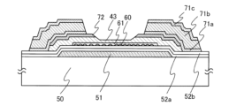
It can be seen that the end of the
次に、図3(A)に示すように、配線71a~71c、ソース領域及びドレイン領域72
、第2のバッファ層43、及びゲート絶縁膜52b上に保護絶縁膜76を形成する。保護
絶縁膜76は、ゲート絶縁膜52a、52bと同様に形成することができる。なお、保護
絶縁膜76は、大気中に浮遊する有機物や金属物、水蒸気などの汚染不純物の侵入を防ぐ
ためのものであり、緻密な膜が好ましい。また、保護絶縁膜76に窒化珪素膜を用いるこ
とで、第2のバッファ層43中の酸素濃度を5×10¹⁹atoms/cm3以下、好ま
しくは1×10¹⁹atoms/cm3以下とすることができ、第2のバッファ層43の
酸化を防止することができる。
Next, as shown in FIG. 3A,
A protective insulating
次に、保護絶縁膜76上に絶縁膜101を形成する。ここでは、感光性の有機樹脂を用い
て絶縁膜101を形成する。次に、第5のフォトマスクを用いて、絶縁膜101を感光し
た後、現像して、保護絶縁膜76を露出する絶縁膜102を形成する。次に、絶縁膜10
2を用いて保護絶縁膜76をエッチングして、図3(B)に示すように、配線71cの一
部を露出するコンタクトホール111と、容量電極71fを露出するコンタクトホール1
12を形成する。
Next, an insulating
3B, the protective insulating
Form 12.
次に、図3(C)に示すように、コンタクトホール111、112に、配線71c及び容
量電極71fに接する画素電極77を形成する。また、ゲート絶縁膜52a、52b、容
量電極71d~71f、及び画素電極77で容量素子106を形成することができる。こ
こでは、絶縁膜102上に導電膜を形成した後、第6のフォトマスクを用いたフォトリソ
グラフィー工程により形成したレジストマスクを用いて導電膜をエッチングして、画素電
極77を形成する。
3C, a
画素電極77は、酸化タングステンを含むインジウム酸化物、酸化タングステンを含むイ
ンジウム亜鉛酸化物、酸化チタンを含むインジウム酸化物、酸化チタンを含むインジウム
錫酸化物、インジウム錫酸化物、インジウム亜鉛酸化物、酸化ケイ素を添加したインジウ
ム錫酸化物などの透光性を有する導電性材料を用いることができる。
The
また、画素電極77として、導電性高分子(導電性ポリマーともいう)を含む導電性組成
物を用いて形成することができる。導電性組成物を用いて形成した画素電極は、シート抵
抗が10000Ω/□以下、波長550nmにおける透光率が70%以上であることが好
ましい。また、導電性組成物に含まれる導電性高分子の抵抗率が0.1Ω・cm以下であ
ることが好ましい。
The
導電性高分子としては、いわゆるπ電子共役系導電性高分子が用いることができる。例え
ば、ポリアニリンまたはその誘導体、ポリピロールまたはその誘導体、ポリチオフェンま
たはその誘導体、若しくはこれらの2種以上の共重合体などがあげられる。
As the conductive polymer, a so-called π-electron conjugated conductive polymer can be used, such as polyaniline or a derivative thereof, polypyrrole or a derivative thereof, polythiophene or a derivative thereof, or a copolymer of two or more of these.
ここでは、画素電極77としては、スパッタリング法によりITOを成膜した後、ITO
上にレジストを塗布する。次に、第6のフォトマスクを用いてレジストを露光及び現像し
、レジストマスクを形成する。次に、レジストマスクを用いてITOをエッチングして画
素電極77を形成する。
Here, the
A resist is applied on the
以上により、薄膜トランジスタを形成することができる。また、表示装置に用いることが
可能な素子基板を形成することができる。
In this manner, a thin film transistor can be formed, and an element substrate that can be used for a display device can be formed.
本実施の形態で作製する薄膜トランジスタのチャネル形成領域は、微結晶半導体膜で形成
されているため、表示装置の駆動周波数を高くすることが可能であり、パネルサイズの大
面積化や画素の高密度化にも十分対応することができる。また、大面積基板において、当
該薄膜トランジスタを作製することができる。
Since the channel formation region of the thin film transistor manufactured in this embodiment mode is formed using a microcrystalline semiconductor film, the driving frequency of the display device can be increased, and the display device can be sufficiently adapted to an increase in the panel size and an increase in pixel density. In addition, the thin film transistor can be manufactured on a large-area substrate.
また、ドナーとなる不純物元素を含む微結晶半導体膜と配線との間に、バッファ層が設け
られているため、ドナーとなる不純物元素を含む微結晶半導体膜と配線との間でのリーク
電流を低減することができる。また、ソース領域及びドレイン領域と、ドナーとなる不純
物元素を含む微結晶半導体膜の間に非晶質半導体膜で形成されるバッファ層が設けられて
いるため、バッファ層が高抵抗領域となり、リーク電流を低減することができる。このた
め、電気特性が優れ、信頼性の高い薄膜トランジスタを作製することができる。
In addition, since a buffer layer is provided between the microcrystalline semiconductor film containing the impurity element serving as a donor and the wiring, leakage current between the microcrystalline semiconductor film containing the impurity element serving as a donor and the wiring can be reduced. In addition, since a buffer layer formed of an amorphous semiconductor film is provided between the source region and the drain region and the microcrystalline semiconductor film containing the impurity element serving as a donor, the buffer layer becomes a high-resistance region, and leakage current can be reduced. Therefore, a thin film transistor with excellent electrical characteristics and high reliability can be manufactured.
また、本実施の形態では、チャネルエッチ型の薄膜トランジスタを用いて示したが、チャ
ネル保護型薄膜トランジスタに本実施の形態を適用することが可能である。
Although a channel-etched thin film transistor is used in this embodiment mode, this embodiment mode can be applied to a channel-protective thin film transistor.
(実施の形態2)
本実施の形態では、実施の形態1と比較して、フォトマスク数を削減することが可能なプ
ロセスを用いて薄膜トランジスタを作製する工程について示す。
(Embodiment 2)
In this embodiment mode, steps for manufacturing a thin film transistor using a process that can reduce the number of photomasks compared to that in Embodiment Mode 1 will be described.
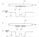
実施の形態1と同様に、図6(A)に示すように、基板50上に導電膜を形成し、導電膜
上にレジストを塗布し、第1のフォトマスクを用いたフォトリソグラフィ工程により形成
したレジストマスクを用いて導電膜の一部をエッチングして、ゲート電極51、容量配線
56を形成する。次に、ゲート電極51上に、ゲート絶縁膜52a、52bを形成する。
次に、ゲート絶縁膜52b上に、第2のフォトマスクを用いたフォトリソグラフィ工程を
用いて、ドナーとなる不純物元素を含む微結晶半導体膜58及び第1のバッファ層62を
形成する。次に、当該第1のバッファ層62上に、第2のバッファ層41、一導電型を付
与する不純物元素が添加された不純物半導体膜55、及び導電膜65a~65cを順に形
成する。次に、導電膜65a上にレジストを塗布する。
6A, a conductive film is formed over a
Next, a
レジストは、ポジ型レジストまたはネガ型レジストを用いることができる。ここでは、ポ
ジ型レジストを用いて示す。
The resist may be a positive resist or a negative resist, and a positive resist is used here.
次に、第3のフォトマスクとして多階調マスクを用いて、レジストに光を照射して、レジ
ストを露光して、レジストマスク81を形成する。
Next, a multi-tone mask is used as a third photomask, and the resist is irradiated with light to expose the resist, thereby forming a resist
ここで、多階調マスクを用いた露光について、図7を用いて説明する。 Here, exposure using a multi-tone mask will be explained with reference to Figure 7.
多階調マスクとは、露光部分、中間露光部分、及び未露光部分に3つの露光レベルを行う
ことが可能なマスクであり、一度の露光及び現像工程により、複数(代表的には二種類)
の厚さの領域を有するレジストマスクを形成することが可能である。このため、多階調マ
スクを用いることで、フォトマスクの枚数を削減することが可能である。
A multi-tone mask is a mask that can perform three exposure levels for the exposed portion, the intermediate exposed portion, and the unexposed portion. It can produce multiple (typically two types)
It is possible to form a resist mask having a region with a thickness of 100 nm to 1000 nm. Therefore, by using a multi-tone mask, it is possible to reduce the number of photomasks.
多階調マスクの代表例としては、図7(A)に示すようなグレートーンマスク159a、
図7(C)に示すようなハーフトーンマスク159bがある。
A typical example of a multi-tone mask is a gray-
There is a half-
図7(A)に示すように、グレートーンマスク159aは、透光性を有する基板163及
びその上に形成される遮光部164並びに回折格子165で構成される。遮光部164に
おいては、光の透光率が0%である。一方、回折格子165はスリット、ドット、メッシ
ュ等の光透過部の間隔を、露光に用いる光の解像度限界以下の間隔とすることにより、光
の透光率を制御することができる。なお、回折格子165は、周期的なスリット、ドット
、メッシュ、または非周期的なスリット、ドット、メッシュどちらも用いることができる
。
7A, the
透光性を有する基板163は、石英等の透光性を有する基板を用いることができる。遮光
部164及び回折格子165は、クロムや酸化クロム等の光を吸収する遮光材料を用いて
形成することができる。
A light-transmitting substrate such as quartz can be used as the light-transmitting
グレートーンマスク159aに露光光を照射した場合、図7(B)に示すように、遮光部
164においては、光透光率166は0%であり、遮光部164及び回折格子165が設
けられていない領域では光透光率166は100%である。また、回折格子165におい
ては、10~70%の範囲で調整可能である。回折格子165における光透光率166の
調整は、回折格子のスリット、ドット、またはメッシュの間隔及びピッチの調整により可
能である。
7B, when the
図7(C)に示すように、ハーフトーンマスク159bは、透光性を有する基板163及
びその上に形成される半透過部167並びに遮光部168で構成される。半透過部167
は、MoSiN、MoSi、MoSiO、MoSiON、CrSiなどを用いることがで
きる。遮光部168は、クロムや酸化クロム等の光を吸収する遮光材料を用いて形成する
ことができる。
As shown in FIG. 7C, the half-
The
ハーフトーンマスク159bに露光光を照射した場合、図7(D)に示すように、遮光部
168においては、光透光率169は0%であり、遮光部168及び半透過部167が設
けられていない領域では光透光率169は100%である。また、半透過部167におい
ては、10~70%の範囲で調整可能である。半透過部167に於ける光透光率169の
調整は、半透過部167の材料により調整により可能である。
7D, when the
多階調マスクを用いて露光した後、現像することで、図6(A)に示すように、膜厚の異
なる領域を有するレジストマスク81を形成することができる。
By performing exposure using a multi-tone mask and then developing, a resist
次に、レジストマスク81により、第2のバッファ層41、一導電型を付与する不純物元
素が添加された不純物半導体膜55、及び導電膜65a~65cをエッチングし分離する
。この結果、図6(B)に示すような、第2のバッファ層42、一導電型を付与する不純
物元素が添加された不純物半導体膜63、及び導電膜85a~85cを形成することがで
きる。なお、図6(A)(レジストマスク81を除く。)は図9(A)のU-Vにおける
断面図に相当する。
Next, the
次に、レジストマスク81をアッシングする。この結果、レジストの面積が縮小し、厚さ
が薄くなる。このとき、膜厚の薄い領域のレジスト(ゲート電極51の一部と重畳する領
域)は除去され、図6(C)に示すように、分離されたレジストマスク86を形成するこ
とができる。
Next, the resist
次に、レジストマスク86を用いて、導電膜85a~85cをエッチングし分離する。こ
の結果、図8(A)に示すような、一対の配線92a~92cを形成することができる。
レジストマスク86を用いて導電膜89a~89cをウエットエッチングすると、導電膜
89a~89cを等方的にエッチングされる。この結果、レジストマスク86より面積の
狭い配線92a~92cを形成することができる。
Next, the
The conductive films 89a to 89c are isotropically etched by wet etching using the resist
次に、図8(B)に示すように、レジストマスク86を用いて、一導電型を付与する不純
物元素が添加された不純物半導体膜63をエッチングして、一対のソース領域及びドレイ
ン領域88を形成する。なお、当該エッチング工程において、第2のバッファ層42の一
部もエッチングされる。一部エッチングされた第2のバッファ層を第2のバッファ層87
と示す。なお、第2のバッファ層87には凹部が形成される。ソース領域及びドレイン領
域の形成工程と、第2のバッファ層の凹部とを同一工程で形成することができる。ここで
は、第2のバッファ層87の一部が、レジストマスク81と比較して面積が縮小したレジ
ストマスク86で一部エッチングされたため、ソース領域及びドレイン領域88の外側に
第2のバッファ層87が突出した形状となる。また、配線92a~92cの端部と、ソー
ス領域及びドレイン領域88の端部は一致せずずれており、配線92a~92cの端部の
外側に、ソース領域及びドレイン領域88の端部が形成される。この後、レジストマスク
86を除去する。なお、図8(B)は、図9(B)のU-Vの断面図に相当する。
8B, the
8B. A recess is formed in the
次に、露出しているバッファ層にダメージが入らず、且つ該バッファ層に対するエッチン
グレートが低い条件でドライエッチングしてもよい。この工程により、ソース領域及びド
レイン領域間のバッファ層上のエッチング残渣物、レジストマスクの残渣、及びレジスト
マスクの除去に用いる装置内の汚染源を除去することが可能であり、ソース領域及びドレ
イン領域間の絶縁を確実なものとすることができる。この結果、薄膜トランジスタのリー
ク電流を低減することが可能であり、オフ電流が小さく、耐圧の高い薄膜トランジスタを
作製することが可能である。なお、エッチングガスには例えば塩素ガスを用いればよい。
Next, dry etching may be performed under conditions that do not damage the exposed buffer layer and have a low etching rate for the buffer layer. This process can remove etching residues on the buffer layer between the source and drain regions, resist mask residues, and contamination sources in the device used to remove the resist mask, and ensure insulation between the source and drain regions. As a result, it is possible to reduce the leakage current of the thin film transistor, and to fabricate a thin film transistor with a small off-current and high breakdown voltage. For example, chlorine gas may be used as the etching gas.
以上の工程により、チャネルエッチ型の薄膜トランジスタ83を形成することができる。
また、2枚のフォトマスクを用いて薄膜トランジスタを形成することができる。
Through the above steps, a channel-etch type
Moreover, a thin film transistor can be formed using two photomasks.
この後、実施の形態1と同様の工程を経て、図8(C)に示すように、配線92a~92
c、ソース領域及びドレイン領域88、第2のバッファ層87、及びゲート絶縁膜52b
上に保護絶縁膜、絶縁膜を形成し、第4のフォトマスクを用いたフォトリソグラフィ工程
により、コンタクトホールを形成する。また、このときの保護絶縁膜を保護絶縁膜76a
と示す。
After that, through the same process as in the first embodiment, the
c, the source region and drain
A protective insulating film and an insulating film are formed on the insulating film 76a, and a contact hole is formed by a photolithography process using a fourth photomask.
This indicates that.
この際、ゲート絶縁膜52bと保護絶縁膜76aとをエッチング選択比が異なる膜で形成
し(例えば、ゲート絶縁膜52bを酸化窒化珪素膜で形成し、保護絶縁膜76aを窒化珪
素膜で形成する。)、保護絶縁膜76aを選択的にエッチングする条件を用いることで、
容量配線56上のコンタクトホール形成のエッチングをゲート絶縁膜52bで止めること
が可能である。このため、容量素子を、容量配線56、ゲート絶縁膜52a、52b、及
び画素電極77で形成することができる。
At this time, the
It is possible to stop the etching for forming the contact hole on the
また、ゲート絶縁膜52b及び保護絶縁膜76aを同じ材料で形成し、ゲート絶縁膜52
aとゲート絶縁膜52bのエッチング選択比を異なる膜で形成する(例えば、ゲート絶縁
膜52b及び保護絶縁膜76aを窒化珪素膜で形成し、ゲート絶縁膜52aを酸化窒化珪
素膜で形成する。)と、保護絶縁膜76a及びゲート絶縁膜52bを選択的にエッチング
する条件を用いることで、容量配線56上のコンタクトホール形成のエッチングを、ゲー
ト絶縁膜52aで止めることができる。このため、容量素子を、容量配線56、ゲート絶
縁膜52a、及び画素電極77で形成することができる。容量素子において、2つの導電
膜(ここでは、容量配線56及び画素電極77)の間の絶縁膜(ここでは、ゲート絶縁膜
52a)の膜厚が薄いほど高い容量を帯びることができるため、好ましい。
In addition, the
When the
次に、絶縁膜102上に、第5のフォトマスクを用いたフォトリソグラフィ工程により画
素電極77を形成することができる。なお、図8(C)は、図9(C)のU-Vの断面図
に相当する。
Next, the
以上により、薄膜トランジスタを作製することができる。また、表示装置に用いることが
可能な素子基板を形成することができる。
In this manner, a thin film transistor can be manufactured, and an element substrate that can be used for a display device can be formed.
以上の工程により、実施の形態1と比較して、フォトマスク数を1枚削減することが可能
な工程により、薄膜トランジスタを有し、表示装置に用いることが可能な素子基板を形成
することができる。
Through the above steps, the number of photomasks can be reduced by one compared to Embodiment Mode 1, and an element substrate which has thin film transistors and can be used for a display device can be formed.
(実施の形態3)
本実施の形態では、実施の形態1及び実施の形態2の薄膜トランジスタと異なる形態につ
いて、以下に示す。
(Embodiment 3)
In this embodiment mode, a different mode from that of the thin film transistors in Embodiments 1 and 2 will be described below.
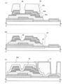
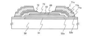
図10は、実施の形態1及び実施の形態2に示す薄膜トランジスタのドナーとなる不純物
元素を含む微結晶半導体膜の代わりに、ゲート絶縁膜52b上にドナーとなる不純物元素
を含む結晶粒60が分散され、ドナーとなる不純物元素を含む結晶粒60及びゲート絶縁
膜52b上を覆うゲルマニウムを主成分とする半導体膜61を有する薄膜トランジスタの
形態を示す。また、ゲルマニウムを主成分とする半導体膜61上面及び側面を覆うバッフ
ァ層43が形成される。シリコンを主成分とする結晶粒60と比較して、ゲルマニウムを
主成分とする半導体膜61のほうが、移動度が高いため、キャリアはゲルマニウムを主成
分とする半導体膜61の方を移動する。このため、ゲート絶縁膜52b上に形成されるゲ
ルマニウムを主成分とする半導体膜61が、薄膜トランジスタのチャネル形成領域として
機能する。
10 shows a form of a thin film transistor having a
また、バッファ層43がゲルマニウムを主成分とする半導体膜61の上面及び側面を覆っ
ているため、ゲルマニウムを主成分とする半導体膜61が配線71a~71cと接せず、
リーク電流を低減することができる。このため、オン電流及び電界効果移動度が高く、オ
フ電流の低い薄膜トランジスタとなる。
In addition, since the
The leakage current can be reduced, and thus a thin film transistor having high on-current and field effect mobility and low off-current can be obtained.
ドナーとなる不純物元素を含む結晶粒60は、実施の形態1と同様に、ゲート絶縁膜52
b上に、ドナーとなる不純物元素を含む微結晶半導体膜または非晶質半導体膜を形成する
。次に、ドナーとなる不純物元素を含む微結晶半導体膜または非晶質半導体膜にプラズマ
を曝して、結晶粒60を形成する。プラズマとしては、水素、フッ素、フッ化物のいずれ
か一つ以上をプラズマCVD装置の反応室内に導入し、高周波電源を印加してプラズマを
発生させる。
The
A microcrystalline semiconductor film or an amorphous semiconductor film containing an impurity element serving as a donor is formed on the substrate 10b. Next, the microcrystalline semiconductor film or the amorphous semiconductor film containing the impurity element serving as a donor is exposed to plasma to form
フッ素、フッ化物気体、または水素の少なくとも一つ以上を導入し高周波電源を印加する
ことで、水素プラズマ、フッ素プラズマが発生する。水素プラズマは、反応室内に水素を
導入し、プラズマを発生させる。フッ素プラズマは、反応室内に、フッ素またはフッ化物
を導入し、プラズマを発生させる。フッ化物としては、HF、SiF4、SiHF3、S
iH2F2、SiH3F、Si2F6、GeF4、GeHF3、GeH2F2、GeH3
F、Ge2F6等がある。なお、フッ素、フッ化物気体、または水素のほかに希ガスを反
応室内に導入して希ガスプラズマを発生させてもよい。
Hydrogen plasma and fluorine plasma are generated by introducing at least one of fluorine, fluoride gas, and hydrogen and applying high-frequency power. Hydrogen plasma is generated by introducing hydrogen into the reaction chamber and generating plasma. Fluorine plasma is generated by introducing fluorine or a fluoride into the reaction chamber and generating plasma. Fluorides include HF, SiF4 , SiHF3 , and S.
iH2F2 , SiH3F , Si2F6 , GeF4 , GeHF3 , GeH2F2 , GeH3
F, Ge 2 F 6 , etc. In addition to fluorine, fluoride gas, or hydrogen, a rare gas may be introduced into the reaction chamber to generate a rare gas plasma.
水素プラズマ、フッ素プラズマ等により、水素ラジカル、フッ素ラジカル等がプラズマ中
に生成する。水素ラジカルは、ドナーとなる不純物元素を含む微結晶半導体膜または非晶
質半導体膜の非晶質成分と反応して、半導体膜の一部を結晶化させるとともに、非晶質成
分をエッチングする。また、フッ素ラジカルは、ドナーとなる不純物元素を含む微結晶半
導体膜または非晶質半導体膜の非晶質成分をエッチングする。このため、結晶性の高い結
晶粒を残存させることができる。また、ゲート絶縁膜52b上にドナーとなる不純物元素
を含む非晶質半導体膜が形成される場合は、非晶質成分をエッチングするとともに、一部
を結晶化し、結晶粒を形成することができる。このため、ゲート絶縁膜との界面における
非晶質成分をもプラズマによりエッチングされるため、ゲート絶縁膜上には結晶粒を形成
することができる。
Hydrogen radicals, fluorine radicals, and the like are generated in the plasma by hydrogen plasma, fluorine plasma, and the like. The hydrogen radicals react with the amorphous components of the microcrystalline semiconductor film or the amorphous semiconductor film containing the impurity element serving as a donor, and crystallize a part of the semiconductor film, while etching the amorphous components. The fluorine radicals etch the amorphous components of the microcrystalline semiconductor film or the amorphous semiconductor film containing the impurity element serving as a donor. This allows crystal grains with high crystallinity to remain. In addition, when an amorphous semiconductor film containing the impurity element serving as a donor is formed on the
プラズマの発生方法は、HF帯(3MHz~30MHz、代表的には13.56MHz、
27.12MHz)、または30MHzより大きく300MHz程度までのVHF帯の高
周波電力、代表的には60MHzを印加することで行われる。また、たとえば周波数が1
GHzや、2.45GHzの高周波プラズマを用いることができる。特に、13.56M
Hzの高周波電力を用いることで、プラズマの均一性を高めることが可能であり、第6世
代~第10世代の大面積基板上においても、均一性の高いプラズマをゲルマニウム膜に曝
すことができるため、大量生産に好ましい。
The plasma generation method is in the HF band (3 MHz to 30 MHz, typically 13.56 MHz,
This is done by applying a high-frequency power in the VHF band of 30 MHz to 300 MHz, typically 60 MHz.
High frequency plasma of 13.56 GHz or 2.45 GHz can be used.
By using high frequency power of 100 Hz, it is possible to improve the uniformity of the plasma, and even on large area substrates of 6th to 10th generations, a germanium film can be exposed to a highly uniform plasma, which is preferable for mass production.
次に、結晶粒60上にゲルマニウムを主成分とする半導体膜61を形成すると、ゲルマニ
ウムを主成分とする半導体膜61の密着性を向上させることができる。さらに、結晶粒6
0を結晶核として結晶成長させて、ゲルマニウムを主成分とする半導体膜61として微結
晶ゲルマニウム膜を形成することができる。
Next, when a
A microcrystalline germanium film can be formed as the
ゲルマニウムを主成分とする半導体膜61をCVD法により形成する場合、ゲルマニウム
を含む堆積性気体と共に、水素をプラズマCVD装置の反応室に導入し、高周波電力を印
加し、プラズマを発生させて、ゲルマニウムを主成分とする半導体膜61として非晶質ゲ
ルマニウム膜または微結晶ゲルマニウム膜を形成する。また、ゲルマニウムを含む堆積性
気体と、水素と共に、シリコンを含む堆積性気体を用いることで、非晶質シリコンゲルマ
ニウム膜または微結晶シリコンゲルマニウム膜を形成する。
When the
なお、ゲルマニウムを主成分とする半導体膜61として非晶質ゲルマニウム膜を形成する
一形態として、反応室において、ゲルマニウムを含む堆積性気体を用いたグロー放電プラ
ズマにより非晶質ゲルマニウム膜を形成することができる。または、ゲルマニウムを含む
堆積性気体に、ヘリウム、アルゴン、クリプトン、ネオンから選ばれた一種または複数種
の希ガス元素で希釈して、グロー放電プラズマにより非晶質ゲルマニウム膜を形成するこ
とができる。または、ゲルマニウムを含む堆積性気体の流量の1倍以上10倍以下、更に
好ましくは1倍以上5倍以下の流量の水素を用いたグロー放電プラズマにより、非晶質ゲ
ルマニウム膜を形成することができる。さらには、ゲルマニウムを含む堆積性気体、水素
と共に、シリコンを含む堆積性気体を用いることで、ゲルマニウムを主成分とする半導体
膜61として非晶質シリコンゲルマニウム膜を形成することができる。
As one form of forming an amorphous germanium film as the
また、ゲルマニウムを主成分とする半導体膜61として微結晶ゲルマニウム膜を形成する
一形態として、反応室内において、ゲルマニウムを含む堆積性気体、ここではゲルマニウ
ムと、水素及び/又は希ガスとを混合し、グロー放電プラズマにより、微結晶ゲルマニウ
ム膜を形成する。ゲルマンは水素及び/又は希ガスで10倍から2000倍に希釈される
。そのため多量の水素及び/又は希ガスが必要とされる。基板の加熱温度は100℃~4
00℃、好ましくは250℃~350℃で行う。さらには、ゲルマニウムを含む堆積性気
体、水素と共に、シリコンを含む堆積性気体を用いることで、ゲルマニウムを主成分とす
る半導体膜61として微結晶シリコンゲルマニウム(SiyGe1-y、0<y<0.5
)膜を形成することができる。
As one mode of forming a microcrystalline germanium film as the
00° C., preferably 250° C. to 350° C. Furthermore, by using a deposition gas containing germanium and a deposition gas containing silicon together with hydrogen, it is possible to obtain a
) film can be formed.
ゲルマニウムを主成分とする半導体膜61の形成工程においてグロー放電プラズマの生成
は、3MHzから30MHz、代表的には13.56MHz、27.12MHzの高周波
電力、または30MHzより大きく300MHz程度までのVHF帯の高周波電力、代表
的には60MHzを印加することで行われる。
In the process of forming the
実施の形態1に示すドナーとなる不純物元素を含む微結晶半導体膜45、及び第1のバッ
ファ層54の代わりに、上記ドナーとなる不純物元素を含む結晶粒及びゲルマニウムを主
成分とする半導体膜を形成した後、実施の形態1と同様の工程により、図10に示すよう
な薄膜トランジスタを作製することができる。また、実施の形態2と同様の工程により薄
膜トランジスタを形成することができる。
Instead of the
また、実施の形態1と異なる形態を図11に示す。実施の形態1と同様に、ゲート絶縁膜
52上にドナーとなる不純物元素を含む微結晶半導体膜45を形成した後、ゲルマニウム
を主成分とする半導体膜を形成する。次に、実施の形態1と同様に第2のフォトマスクを
用いたフォトリソグラフィ工程により形成したレジストマスクを用いて、ドナーとなる不
純物元素を含む微結晶半導体膜45及びゲルマニウムを主成分とする半導体膜をエッチン
グして、ドナーとなる不純物元素を含む微結晶半導体膜69、及びゲルマニウムを主成分
とする半導体膜61を形成する。次に、実施の形態1と同様の工程により、図11に示す
ような、ゲート絶縁膜52b上にドナーとなる不純物元素を含む微結晶半導体膜69が形
成され、その上にゲルマニウムを主成分とする半導体膜61が形成され、ドナーとなる不
純物元素を含む微結晶半導体膜69及びゲルマニウムを主成分とする半導体膜61の側面
を覆うバッファ層73を有する薄膜トランジスタを作製することができる。また、実施の
形態2と同様の工程により薄膜トランジスタを形成することができる。
11 shows a different embodiment from that of the first embodiment. As in the first embodiment, a
また、ゲルマニウムを主成分とする半導体膜61は、シリコンを主成分とする微結晶半導
体膜69と接するため、これらの密着性が向上する。このため、薄膜トランジスタの歩留
まりを高めることが可能である。
In addition, the
また、ドナーとなる不純物元素を含む微結晶半導体膜69は膜表面においては微結晶が形
成されるため、ドナーとなる不純物元素を含む微結晶半導体膜69の表面は結晶性が高い
。この上にゲルマニウムを主成分とする半導体膜61を形成すると、シリコンを主成分と
する微結晶半導体膜69の表面の結晶を結晶核として、結晶成長するため、結晶性の高い
ゲルマニウムを主成分とする半導体膜61、代表的にはゲルマニウムを主成分とする微結
晶半導体膜が形成される。ゲルマニウムを主成分とする半導体膜61は抵抗率が低いため
、キャリアは優先的にゲルマニウムを主成分とする半導体膜61側を流れる。このため、
本実施の形態で示す薄膜トランジスタは、電界効果移動度やオン電流が高い。
Furthermore, since microcrystals are formed on the surface of the
The thin film transistor described in this embodiment has high field-effect mobility and high on-state current.
また、バッファ層73がゲルマニウムを主成分とする半導体膜61の上面及び側面を覆っ
ているため、ゲルマニウムを主成分とする半導体膜61が配線71a~71cと接しない
ため、リーク電流の発生を抑制することができる。このため、オン電流及び電界効果移動
度が高く、オフ電流の低い薄膜トランジスタを作製することができる。
In addition, since the
(実施の形態4)
本実施の形態では、上記実施の形態で示す薄膜トランジスタの構造について、以下に示す
。
(Embodiment 4)
In this embodiment mode, a structure of the thin film transistor shown in the above embodiment mode will be described below.
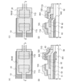
図12(A)は、ソース電極及びドレイン電極が平行な場合の薄膜トランジスタの上面構
造であり、図12(B)は、図12(A)のE-Fの断面図を示す。
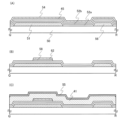
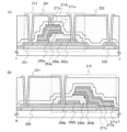
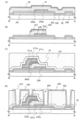
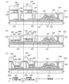
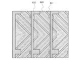
12A shows a top view of a thin film transistor in which a source electrode and a drain electrode are parallel to each other, and FIG. 12B shows a cross-sectional view taken along line EF of FIG. 12A.
図12(B)は、基板50上にゲート電極51及びゲート絶縁膜が形成され、ゲート電極
の内側にドナーとなる不純物元素を含む微結晶半導体膜58及び第1のバッファ層62が
形成される。また、ドナーとなる不純物元素を含む微結晶半導体膜58及び第1のバッフ
ァ層62を覆う第2のバッファ層43が形成される。また、第2のバッファ層43上に対
向するソース領域72S及びドレイン領域72Dと、ソース電極71S及びドレイン電極
71Dが形成される。
12B, a
図12(B)においては、ゲート電極51及びドレイン領域72Dの重畳領域441と、
ドナーとなる不純物元素を含む微結晶半導体膜58及びドレイン領域72Dの重畳領域4
42とを有す。また、重畳領域441、442も重なっている。
In FIG. 12B, an overlapping
The overlapping region 4 of the
42. In addition, overlapping
図12(A)及び(B)に示す薄膜トランジスタ、ゲート電極51及びドレイン領域72
D、並びにドナーとなる不純物元素を含む微結晶半導体膜58及びドレイン領域72Dが
重畳しているため、オン電流が高く、電界効果移動度が高い薄膜トランジスタとすること
ができる。
The thin film transistor,
Since the
図12(C)は、薄膜トランジスタの上面構造であり、図12(D)は、図12(C)の
E-Fの断面図を示す。
FIG. 12C shows a top view of a thin film transistor, and FIG. 12D shows a cross-sectional view taken along line EF of FIG. 12C.
図12(C)は、基板50上にゲート電極51及びゲート絶縁膜が形成され、ゲート電極
の端部を覆うようにドナーとなる不純物元素を含む微結晶半導体膜58及び第1のバッフ
ァ層62が形成される。また、ドナーとなる不純物元素を含む微結晶半導体膜58及び第
1のバッファ層62を覆う第2のバッファ層43が形成される。また、第2のバッファ層
43上に対向するソース領域72S及びドレイン領域72Dと、ソース電極71S及びド
レイン電極71Dが形成される。
12C, a
図12(D)においては、ゲート電極51の端部及びドレイン電極71Dの端部が一致し
、ドナーとなる不純物元素を含む微結晶半導体膜58及びドレイン領域72Dの重畳領域
444を有す。
In FIG. 12D, an edge of the
図12(B)においては、ゲート電極51の端部及びドレイン電極71Dの端部が一致し
ている。一方、ドナーとなる不純物元素を含む微結晶半導体膜58及びドレイン領域72
Dの重畳領域444を有す。
12B, an edge of the
図12(C)及び(D)に示す薄膜トランジスタは、ゲート電極51及びドレイン領域7
2Dが重畳していないため、寄生容量を低減することができる。このため、ドレイン電極
側の電圧降下を低減する薄膜トランジスタとすることができる。このため、当該構造を用
いた表示装置は、画素の応答速度を向上させることができる。特に、液晶表示装置の画素
に形成される薄膜トランジスタの場合、ドレイン電圧の電圧降下を低減できるため、液晶
材料の応答速度を上昇させることが可能である。
The thin film transistor shown in FIGS. 12C and 12D has a
Since 2D does not overlap, the parasitic capacitance can be reduced. Therefore, a thin film transistor that reduces the voltage drop on the drain electrode side can be obtained. Therefore, a display device using this structure can improve the response speed of the pixel. In particular, in the case of a thin film transistor formed in a pixel of a liquid crystal display device, the voltage drop of the drain voltage can be reduced, so that the response speed of the liquid crystal material can be increased.
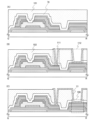
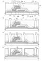
図13(A)は、ソース電極及びドレイン電極の対向領域が曲線状であり、ソース電極ま
たはドレイン電極がC字またはU字の場合の薄膜トランジスタの上面構造であり、図13
(B)は、図13(A)のG-Hの断面図を示し、図13(C)は図13(A)のE-F
の断面図を示す。
FIG. 13A shows a top view structure of a thin film transistor in which the opposing regions of a source electrode and a drain electrode are curved and the source electrode or the drain electrode is C-shaped or U-shaped.
FIG. 13B is a cross-sectional view taken along line GH in FIG. 13A, and FIG. 13C is a cross-sectional view taken along line EF in FIG. 13A.
A cross-sectional view of the above is shown.
図13(B)及び図13(C)は、基板50上にゲート電極51及びゲート絶縁膜が形成
され、ゲート電極の内側にドナーとなる不純物元素を含む微結晶半導体膜58及び第1の
バッファ層62が形成される。また、ドナーとなる不純物元素を含む微結晶半導体膜58
及び第1のバッファ層62を覆う第2のバッファ層43が形成される。また、第2のバッ
ファ層43上に対向するソース領域及びドレイン領域72と、ソース電極71S及びドレ
イン電極71Dが形成される。
13B and 13C, a
A
図13(B)及び図13(C)においては、ゲート電極51及びドレイン領域72Dの重
畳領域449と、ドナーとなる不純物元素を含む微結晶半導体膜58及びドレイン領域7
2Dの重畳領域450とを有す。また、重畳領域449、450も重なっている。また、
配線の一方はソース領域及びドレイン領域の他方を囲む形状(具体的には、U字型、C字
型)である。このため、キャリアが移動する領域の面積を増加させることが可能であるた
め、電流量を増やすことが可能であり、薄膜トランジスタの面積を縮小することができる
。
13B and 13C, the
The overlapping
One of the wirings is shaped to surround the other of the source and drain regions (specifically, U-shaped or C-shaped), which makes it possible to increase the area of the region through which carriers move, thereby increasing the amount of current and reducing the area of the thin film transistor.
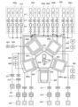
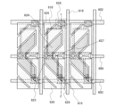
(実施の形態5)
本実施の形態では、図14に示す素子基板1300において、画素部1331と入力端子
1332、1333との間に形成される保護回路1334、1336の構成及びその作製
方法について、以下に示す。本実施の形態で示す保護回路は、ショットキー接合されたダ
イオードを用いて形成する。
(Embodiment 5)
In this embodiment mode, the structure and manufacturing method of
基板1330上に形成された走査線側の入力端子1332及び信号線側の入力端子133
3と、画素部1331とは縦横に延びた配線によって接続されており、該配線は保護回路
1334~1337に接続されている。
An
The
画素部1331と、入力端子1332とは配線1339によって接続されている。保護回
路1334は、画素部1331と、入力端子1332との間に配置され、配線1339に
接続されている。保護回路1334によって、画素部1331が有する薄膜トランジスタ
等の各種半導体素子を保護し、劣化又は破壊することを防止することができる。なお、配
線1339は、図中では一の配線を指し示しているが、配線1339と平行に設けられて
いる複数の配線のすべてが配線1339と同様の接続関係を有する。なお、配線1339
は、走査線(ゲート配線)として機能する。
The
functions as a scanning line (gate wiring).
なお、走査線側の保護回路1334は、入力端子1332と画素部1331との間に設け
られている保護回路1334のみならず、画素部1331を挟んで入力端子1332の反
対側にも設けられていても良い(図14の保護回路1335を参照)。
In addition, the
また、画素部1331と、入力端子1333とは配線1338によって接続されている。
保護回路1336は、画素部1331と、入力端子1333との間に配置され、配線13
38に接続されている。保護回路1336によって、画素部1331が有する薄膜トラン
ジスタ等の各種半導体素子を保護し、劣化又は破壊を防止することができる。なお、配線
1338は、図中では一の配線を指し示しているが、配線1338と平行に設けられてい
る複数の配線のすべてが配線1338と同様の接続関係を有する。なお、配線1338は
、信号線(ソース配線)として機能する。
The
The
38. The
なお、信号線側の保護回路1336は、入力端子1333と画素部1331との間に設け
られている保護回路1336のみならず、画素部1331を挟んで入力端子1333の反
対側にも設けられていても良い(図14の保護回路1337を参照)。
In addition, the
なお、保護回路1334~1337は全て設ける必要はないが、少なくとも保護回路13
34は設ける必要がある。走査線である配線1339に過大な電流が生じることで、画素
部1331が有する薄膜トランジスタのゲート絶縁膜が破壊され、点欠陥を生じうるから
である。
It is not necessary to provide all of the
It is necessary to provide the wiring 34 because an excessive current generated in the
更には、保護回路1334のみならず保護回路1336を設けることで信号線である配線
1338に過大な電流が生じることを防止することができる。そのため、保護回路133
4のみを設ける場合と比較して、信頼性が向上し、歩留まりが向上する。保護回路133
6を有することで、薄膜トランジスタ形成後のラビング工程にて生じうる、静電気による
破壊を防止することもできる。
Furthermore, by providing not only the
The reliability and yield are improved compared to the case where only the protection circuit 133 is provided.
By providing the insulating layer 6, it is possible to prevent damage caused by static electricity that may occur in a rubbing step after the formation of a thin film transistor.
更には、保護回路1335及び保護回路1337を有することで、信頼性を更に向上させ
、歩留まりを向上させることができる。保護回路1335及び保護回路1337は、入力
端子1332及び入力端子1333とは反対側に設けられているため、これらは表示装置
の作製工程中に生じる、各種半導体素子の劣化又は破壊の防止に寄与する。
Furthermore, reliability can be further improved and yield can be improved by providing the
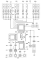
次に、図14における保護回路1334~1337に用いられる保護回路の具体的な回路
構成の例について、以下に説明する。
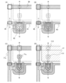
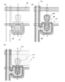
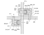
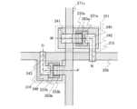
Next, an example of a specific circuit configuration of the
図15に示す保護回路は、複数のダイオードを有する。保護回路は、それぞれ信号線27
1c(図14に示す、信号線である配線1338)に接続されるダイオード311、31
2を有する。ここで、図15のI-Jの断面図を図16(A)に示し、図15のK-Lの
断面図を図16(B)に示す。
The protection circuit shown in FIG. 15 includes a plurality of diodes.
1c (the
16A shows a cross-sectional view taken along line IJ in FIG 15, and FIG 16B shows a cross-sectional view taken along line KL in FIG 15.
図16(A)に示すように、ダイオード311の信号線271a~271cは、導電膜2
01を介してゲート電極251と接続されると共に、ソース領域またはドレイン領域26
3aに接する。また、ダイオード311の第2のバッファ層242aは、導電膜202を
介してコモン線256に接続される。ここでは、コモン線256は、導電膜202を介し
て、ドナーとなる不純物元素が添加されていない非晶質半導体膜で形成される第2のバッ
ファ層242aと接するため、ショットキー接合している。
As shown in FIG. 16A, the
01 and is connected to the
3a. The
また、図16(B)に示すように、ダイオード312のゲート電極は、コモン線256で
形成され、コモン線256は、導電膜203を介してダイオード312の第2のバッファ
層242bに接続される。また、ダイオード312の信号線271a~271cは、ソー
ス領域またはドレイン領域263bに接する。ここでは、コモン線256は、導電膜20
3を介して、ドナーとなる不純物元素が添加されていない非晶質半導体膜で形成される第
2のバッファ層242aと接するため、ショットキー接合している。
16B, the gate electrode of the
Since the
信号線271a~271cの入力端子から絶対値の大きい正の電圧が印加されると、図1
6(A)のダイオード311のゲート電極251及び信号線271a~271cに正の電
圧がかかり、ドナーとなる不純物元素を含む微結晶半導体膜258aにキャリアが発生し
、コモン線256に電流が流れる。また、信号線271a~271cの入力端子から絶対
値の大きい負の電圧が印加されると、図16(B)のダイオード312の信号線271a
~271cに負の電圧がかかり、ゲート電極及び信号線271a~271cでしきい値電
圧以上の電位差が生じるため、ドナーとなる不純物元素を含む微結晶半導体膜258bに
キャリアが発生し、コモン線256に電流が流れる。このため、画素部に設けられる薄膜
トランジスタの静電破壊を防止することができる。
When a positive voltage with a large absolute value is applied to the input terminals of the
16A and the
A negative voltage is applied to the
次に、図16(A)に示すダイオード311の作製工程について、図17を用いて説明す
る。ここでは、実施の形態1を用いてダイオード311の作製方法を示すが、実施の形態
2を適宜用いることができる。
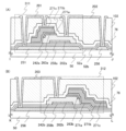
Next, a manufacturing process of the
実施の形態1と同様の工程により、図17(A)に示すように、基板50上にゲート電極
251及びコモン線256を形成する。次に、ゲート電極251、コモン線256上にゲ
ート絶縁膜52a、52bを形成する。
17A, a
次に、実施の形態1と同様に、ゲート絶縁膜52b上にドナーとなる不純物元素を含む微
結晶半導体膜258a、及び第1のバッファ層262aを形成する。
Next, in a manner similar to that of Embodiment Mode 1, a
次に、実施の形態1と同様に、第1のバッファ層262a及びゲート絶縁膜52b上に第
2のバッファ層242aを形成する。
Next, in the same manner as in the first embodiment, a
次に、実施の形態1と同様に、ソース領域またはドレイン領域263aと信号線271a
~271cを形成する。この場合、信号線271a~271cに覆われていない第2のバ
ッファ層242aは一部膜厚が薄くなる。
Next, in the same manner as in the first embodiment, the source or drain
In this case, the thickness of the
次に、実施の形態1と同様に、保護絶縁膜76及び絶縁膜101を形成する。
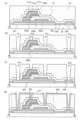
Next, similarly to embodiment 1, the protective insulating
次に、図17(B)に示すように、ゲート絶縁膜52bを露出するコンタクトホール21
1、214、信号線271cを露出するコンタクトホール212、第2のバッファ層24
2aを露出するコンタクトホール213を形成する。
Next, as shown in FIG. 17B, a contact hole 21 exposing the
1, 214, a
A
次に、図17(C)に示すように、ゲート絶縁膜52a、52bを選択的にエッチングす
る条件を用いて、ゲート絶縁膜52a、52bをエッチングして、ゲート電極251及び
コモン線256を露出するコンタクトホール215、216を形成する。
Next, as shown in FIG. 17C, the
次に、図17(D)に示すように、画素電極77を形成すると同時に、ゲート電極251
及び信号線271cを接続する導電膜201、並びに第2のバッファ層242a及びコモ
ン線256を接続する導電膜202を形成する。
Next, as shown in FIG. 17D, the
A
以上の工程により、ダイオード311を形成することができる。また、実施の形態1乃至
実施の形態3に示す薄膜トランジスタと同様のマスク数により保護回路を形成することが
できる。
Through the above steps, the
(実施の形態6)
本実施の形態では、実施の形態5とは異なる保護回路の構造及び作製方法について、以下
に示す。本実施の形態では、ドナーとなる不純物元素を含む微結晶半導体膜、第1のバッ
ファ層、及び第2のバッファ層と、コモン線とでショットキー接合するダイオードを用い
て示す。
(Embodiment 6)
In this embodiment mode, a structure and a manufacturing method of a protection circuit, which are different from those in Embodiment Mode 5, will be described below. In this embodiment mode, a microcrystalline semiconductor film containing an impurity element which serves as a donor, a first buffer layer, a second buffer layer, and a diode which forms a Schottky junction with a common line will be described.
ここで、図15のI-Jの断面図を図18(A)に示し、図15のK-Lの断面図を図1
8(B)に示す。
Here, a cross-sectional view taken along line IJ in FIG. 15 is shown in FIG. 18A, and a cross-sectional view taken along line KL in FIG. 15 is shown in FIG.
8(B).
図18(A)に示すように、ダイオード313の信号線271a~271cは、導電膜2
01を介してゲート電極251と接続されると共に、ソース領域またはドレイン領域26
3aに接する。また、ダイオード313のドナーとなる不純物元素を含む微結晶半導体膜
258a、第1のバッファ層262a、及び第2のバッファ層242aは、導電膜222
を介してコモン線256に接続される。ここでは、コモン線256は、導電膜222を介
して、ドナーとなる不純物元素が添加されていない非晶質半導体膜で形成される第1のバ
ッファ層262a及び第2のバッファ層242a、並びに低濃度のドナーとなる不純物元
素を含む微結晶半導体膜258aと接するため、ショットキー接合している。
As shown in FIG. 18A, the
01 and is connected to the
In addition, the
Here, the
また、図18(B)に示すように、ダイオード314のゲート電極は、コモン線256で
形成され、コモン線は256は、導電膜221を介してダイオード314の、ドナーとな
る不純物元素を含む微結晶半導体膜258b、第1のバッファ層262b、及び第2のバ
ッファ層242bに接続される。また、ダイオード314の信号線271a~271cは
、ソース領域またはドレイン領域263bに接する。ここでは、コモン線256は、導電
膜221を介して、ドナーとなる不純物元素が添加されていない非晶質半導体膜で形成さ
れる第1のバッファ層262b、及び第2のバッファ層242b、並びに低濃度のドナー
となる不純物元素を含む微結晶半導体膜258bと接するため、ショットキー接合してい
る。
18B, a gate electrode of the
なお、図15に示す、走査線である配線1339に設けられる保護回路の場合は、図18
の信号線271a~271cがコモン線として機能し、図18のコモン線256は走査線
として機能する。
In the case of a protection circuit provided for the
18 functions as a scanning line. The
信号線271a~271cの入力端子から正の高電圧が印加されると、図18(A)のダ
イオード313のゲート電極251及び信号線271a~271cに正の電圧がかかり、
ドナーとなる不純物元素を含む微結晶半導体膜258aにキャリアが発生し、コモン線2
56に電流が流れる。また、信号線271a~271cの入力端子から絶対値の大きい負
の電圧が印加されると、図18(B)のダイオード314の信号線271a~271cの
負の電圧がかかり、ゲート電極及び信号線271a~271cにしきい値電圧以上の電位
差が生じるため、ドナーとなる不純物元素を含む微結晶半導体膜258bにキャリアが発
生し、コモン線256に電流が流れる。このため、画素部に設けられる薄膜トランジスタ
の静電破壊を防止することができる。
When a positive high voltage is applied from the input terminals of the
Carriers are generated in the
18B is applied to the
次に、図18(A)に示すダイオード313の作製工程について、図19を用いて説明す
る。ここでは、実施の形態1を用いてダイオード313の作製方法を示すが、実施の形態
2を適宜用いることができる。
Next, a manufacturing process of the
実施の形態5と同様に、図19(A)に示すように、基板50上にゲート電極251及び
コモン線256を形成する。次に、ゲート電極251、コモン線256上にゲート絶縁膜
52a、52bを形成する。次に、ゲート絶縁膜52b上にドナーとなる不純物元素を含
む微結晶半導体膜258a、及び第1のバッファ層262aを形成する。第1のバッファ
層262a及びゲート絶縁膜52b上に第2のバッファ層242aを形成する。次に、信
号線271a~271cと、ソース領域またはドレイン領域263aを形成する。この場
合、信号線271a~271cに覆われていない第2のバッファ層242aは一部膜厚が
薄くなる。次に、保護絶縁膜76及び絶縁膜101を形成する。なお、ここでは、絶縁膜
101として、非感光性樹脂を用いることが好ましい。
Similarly to the embodiment mode 5, as shown in FIG. 19A, a
次に、絶縁膜101上にレジストを塗布する。次に、実施の形態2に示すような多階調マ
スクを用いて、レジストに光を照射して、レジストを露光し、現像して、複数の厚さを有
するレジストマスク223を形成する。ここでは、ゲート電極251、信号線271a~
271c、及びコモン線256を露出するコンタクトホールの形成領域においては、レジ
ストを100%露光することが可能であり、また、ドナーとなる不純物元素を含む微結晶
半導体膜258a、及び第1のバッファ層262a、第2のバッファ層242aを露出す
るコンタクトホールの形成領域においては、レジストを10~70%の範囲で露光するこ
とが可能な多階調マスクを用いることで、厚さの異なるレジストマスク223を形成する
ことができる。
Next, a resist is applied onto the insulating
In the formation regions of the contact holes exposing 271c and the
次に、図19(B)に示すように、レジストマスク223を用いて絶縁膜101をエッチ
ングする。次に、保護絶縁膜76をエッチングする。次に、ゲート絶縁膜52a、52b
を選択的にエッチングする。この結果、ゲート電極251、コモン線256を露出するコ
ンタクトホール224、226と、信号線271cを露出するコンタクトホール225を
形成することができる。
19B, the insulating
As a result, contact holes 224 and 226 exposing the
次に、レジストマスク223をアッシングし、後退させることで、膜厚の薄い領域が分離
されたレジストマスク231を形成する。次に、当該マスクを用いて絶縁膜101及び保
護絶縁膜76をエッチングする。次に、ドナーとなる不純物元素を含む微結晶半導体膜2
58a、及び第1のバッファ層262a、第2のバッファ層242aのそれぞれ一部をエ
ッチングして、図19(C)に示すような、ゲート絶縁膜52bを露出するコンタクトホ
ール234を形成する。この際、ゲート絶縁膜52bがエッチングされない条件で、絶縁
膜101、保護絶縁膜76、ドナーとなる不純物元素を含む微結晶半導体膜258a、及
び第1のバッファ層262a、第2のバッファ層242aのそれぞれ一部をエッチングこ
とが好ましい。また、当該エッチング工程により、図19(B)に示すコンタクトホール
224~226においても、絶縁膜102及び保護絶縁膜76の一部がエッチングされ、
上面形状が二重のコンタクトホール232、234、235を形成する。
Next, the resist
19C, the insulating
Contact holes 232, 234, and 235 are formed with a double top surface shape.
この後、実施の形態5と同様に、画素電極を形成すると同時に、ゲート電極251及び信
号線271cを接続する導電膜201、並びに第2のバッファ層242a及びコモン線2
56を接続する導電膜222を形成する。
Thereafter, in the same manner as in the fifth embodiment, a pixel electrode is formed, and at the same time, a
A
以上の工程により、ダイオードを形成することができる。また、実施の形態1乃至実施の
形態3に示す薄膜トランジスタと同様のマスク数により保護回路を形成することができる
。
Through the above steps, a diode can be formed. In addition, a protection circuit can be formed using the same number of masks as those for the thin film transistors described in any of Embodiments 1 to 3.
(実施の形態7)
本実施の形態では、実施の形態5及び実施の形態6とは異なる保護回路の構造及び作製方
法について、以下に示す。本実施の形態では、ドナーとなる不純物元素を含む微結晶半導
体膜、第1のバッファ層、及び第2のバッファ層でショットキー接合するダイオードを用
いて示す。
(Seventh embodiment)
In this embodiment mode, a structure and a manufacturing method of a protection circuit different from those in Embodiment Mode 5 and Embodiment Mode 6 will be described below. In this embodiment mode, a microcrystalline semiconductor film containing an impurity element which serves as a donor, a first buffer layer, and a diode which forms a Schottky junction with a second buffer layer are used.
ここで、図20のM-Nの断面図を図21(A)に示し、図20のO-Pの断面図を図2
1(B)に示す。
Here, a cross-sectional view taken along line MN in FIG. 20 is shown in FIG. 21A, and a cross-sectional view taken along line OP in FIG. 20 is shown in FIG.
1(B).
図20に示すように、本実施の形態のダイオード315は、コモン線256と、ドナーと
なる不純物元素を含む微結晶半導体膜231a、第1のバッファ層232a、及び第2の
バッファ層233aとが接するコンタクトホール245が、ドナーとなる不純物元素を含
む微結晶半導体膜231a、第1のバッファ層232a、及び第2のバッファ層233a
の端部に形成されている点が実施の形態6と異なる。同様に、ダイオード316は、コモ
ン線256と、ドナーとなる不純物元素を含む微結晶半導体膜231b、第1のバッファ
層232b、及び第2のバッファ層233bとが接するコンタクトホール246が、ドナ
ーとなる不純物元素を含む微結晶半導体膜231b、第1のバッファ層232b、及び第
2のバッファ層233bの端部に形成されている点が実施の形態6と異なる。
As shown in FIG. 20 , in the
Similarly, the
図21(A)に示すように、ダイオード315の信号線271a~271cは、導電膜2
41を介してゲート電極251と接続されると共に、ソース領域またはドレイン領域26
3aに接する。また、ダイオード315のドナーとなる不純物元素を含む微結晶半導体膜
231a、第1のバッファ層232a、及び第2のバッファ層233aは、導電膜242
を介してコモン線256に接続される。ここでは、コモン線256は、導電膜242を介
して、ドナーとなる不純物元素が添加されていない非晶質半導体膜で形成される第1のバ
ッファ層232a及び第2のバッファ層233a、並びに低濃度のドナーとなる不純物元
素を含む微結晶半導体膜231aと接するため、ショットキー接合している。
As shown in FIG. 21A, the
41 and is connected to the
The
Here, the
また、ダイオード316のゲート電極は、コモン線256で形成され、コモン線256は
、導電膜243を介してダイオード316の、ドナーとなる不純物元素を含む微結晶半導
体膜231b、第1のバッファ層232b、及び第2のバッファ層233bに接続される
。また、ダイオード316の信号線271a~271cは、ソース領域またはドレイン領
域263bに接する。ここでは、コモン線256は、導電膜243を介して、ドナーとな
る不純物元素が添加されていない非晶質半導体膜で形成される第1のバッファ層232b
、及び第2のバッファ層233a、並びに低濃度のドナーとなる不純物元素を含む微結晶
半導体膜231bと接するため、ショットキー接合している。
A gate electrode of the
, the
なお、図15に示す、走査線である配線1339に設けられる保護回路の場合は、図21
の信号線271a~271cがコモン線として機能し、図21のコモン線256は走査線
として機能する。
In the case of a protection circuit provided for the
The
信号線271a~271cの入力端子から正の高電圧が印加されると、図21(A)のダ
イオード315のゲート電極251及び信号線271a~271cに正の電圧がかかり、
ドナーとなる不純物元素を含む微結晶半導体膜231aにキャリアが発生し、コモン線2
56に電流が流れる。また、信号線271a~271cの入力端子から絶対値の大きい負
の電圧が印加されると、図21(B)のダイオード316の信号線271a~271cの
負の電圧がかかり、コモン線256及び信号線271a~271cにしきい値電圧以上の
電位差が生じるため、ドナーとなる不純物元素を含む微結晶半導体膜231bにキャリア
が発生し、コモン線256に電流が流れる。このため、画素部に設けられる薄膜トランジ
スタの静電破壊を防止することができる。
When a positive high voltage is applied from the input terminals of the
Carriers are generated in the
21B is applied to the
次に、図21(A)に示すダイオード315の作製工程について、図22を用いて説明す
る。ここでは、実施の形態1を用いてダイオード315の作製方法を示すが、実施の形態
2を適宜用いることができる。
Next, a manufacturing process of the
実施の形態5と同様に、図22(A)に示すように、基板50上にゲート電極251及び
コモン線256を形成する。次に、ゲート電極251、コモン線256上にゲート絶縁膜
52a、52bを形成する。次に、ゲート絶縁膜52b上にドナーとなる不純物元素を含
む微結晶半導体膜258a、及び第1のバッファ層262aを形成する。第1のバッファ
層262a及びゲート絶縁膜52b上に第2のバッファ層41を形成する。次に、第2の
バッファ層41上に、一導電型を付与する不純物元素が添加された不純物半導体膜55を
形成する。
22A, a
次に、一導電型を付与する不純物元素が添加された不純物半導体膜55上にレジストを塗
布した後、フォトマスクを用いたフォトリソグラフィ工程によりレジストマスクを形成す
る。次に、当該レジストマスクを用いて一導電型を付与する不純物元素が添加された不純
物半導体膜55、第2のバッファ層44、第1のバッファ層262a、ドナーとなる不純
物元素を含む微結晶半導体膜258aのそれぞれ一部をエッチングして、図22(B)に
示すような、ドナーとなる不純物元素を含む微結晶半導体膜235、第1のバッファ層2
36、第2のバッファ層237、及び一導電型を付与する不純物元素が添加された不純物
半導体膜238を形成する。ここでは、ドナーとなる不純物元素を含む微結晶半導体膜2
35及び第1のバッファ層236の側面は、第2のバッファ層237に覆われる領域と、
第2のバッファ層237の側面と概略一致する領域とを有する。
Next, a resist is applied onto the
36, a
35 and the side of the
The
次に、実施の形態6と同様に、信号線271a~271cと、ソース領域またはドレイン
領域263aを形成する。この場合、信号線271a~271cに覆われていない第2の
バッファ層239は一部膜厚が薄くなる。次に、保護絶縁膜76及び絶縁膜101を形成
する。
Next, the
次に、実施の形態6と同様に多階調マスクを用いた工程により、ゲート電極251、コモ
ン線256、信号線271cそれぞれを露出するコンタクトホールを形成する。また、ド
ナーとなる不純物元素を含む微結晶半導体膜231a、第1のバッファ層232a、第2
のバッファ層233aのそれぞれ一部をエッチングして、ドナーとなる不純物元素を含む
微結晶半導体膜235、第1のバッファ層236、及び第2のバッファ層237の側面を
露出すると共に、ゲート絶縁膜52bを露出するコンタクトホール245を形成する。
Next, contact holes exposing the
The
この後、実施の形態5と同様に、画素電極を形成すると同時に、ゲート電極251及び信
号線271cを接続する導電膜241、並びにドナーとなる不純物元素を含む微結晶半導
体膜231a、第1のバッファ層232a、及び第2のバッファ層233a、及びコモン
線256を接続する導電膜242を形成する。
After that, similarly to Embodiment 5, a pixel electrode is formed, and at the same time, a
以上の工程により、ダイオード315を形成することができる。また、実施の形態1乃至
実施の形態3に示す薄膜トランジスタと同様のマスク数により保護回路を形成することが
できる。
Through the above steps, the
(実施の形態8)
本実施の形態では、上記実施の形態での成膜工程に用いることが可能な成膜装置及びそこ
での基板の流れを以下に示す。
(Embodiment 8)
In this embodiment mode, a film formation apparatus that can be used in the film formation process in the above embodiment mode and a flow of a substrate therein will be described below.
次に、本実施の形態の成膜工程に適用されるプラズマCVD装置の一例として、ゲート絶
縁膜、ドナーとなる不純物元素を含む微結晶半導体膜、バッファ層、一導電型を付与する
不純物元素が添加された不純物半導体膜の成膜に適した構成の一例を示す。
Next, as an example of a plasma CVD apparatus applied to the film formation process of this embodiment, an example of a configuration suitable for forming a gate insulating film, a microcrystalline semiconductor film containing an impurity element serving as a donor, a buffer layer, and an impurity semiconductor film to which an impurity element imparting one conductivity type is added will be described.
図23は複数の反応室を備えたマルチ・チャンバ・プラズマCVD装置の一例を示す。こ
の装置は共通室423と、ロード/アンロード室422、第1反応室400a、第2反応
室400b、第3反応室400c、第4反応室400dを備えた構成となっている。ロー
ド/アンロード室422のカセットに装填される基板は、共通室423の搬送機構426
によって各反応室に搬出入される枚葉式の構成である。共通室423と各室の間にはゲー
トバルブ425が備えられ、各反応室で行われる処理が、相互に干渉しないように構成さ
れている。
23 shows an example of a multi-chamber plasma CVD apparatus equipped with multiple reaction chambers. This apparatus is configured with a
A
各反応室は形成する薄膜の種類によって区分されている。例えば、第1反応室400aは
ゲート絶縁膜などの絶縁膜を成膜し、第2反応室400bは、ドナーとなる不純物元素を
含む微結晶半導体膜を成膜し、第3反応室400cは薄膜トランジスタの高抵抗領域とな
るバッファ層を成膜し、第4反応室400dはソース及びドレインを形成する一導電型を
付与する不純物元素が添加された不純物半導体膜を成膜する反応室として充当される。勿
論、反応室の数はこれに限定されるわけではなく、必要に応じて任意に増減することがで
きる。
Each reaction chamber is classified according to the type of thin film to be formed. For example, the
各反応室には排気手段としてターボ分子ポンプ419とドライポンプ420が接続されて
いる。排気手段はこれらの真空ポンプの組み合わせに限定されるものではなく、概略10
-1Paから10-5Paの真空度にまで排気できるものであれば他の真空ポンプを適用
することができる。排気手段と各反応室との間にはバタフライバルブ417が設けられて
おり、これによって真空排気を遮断させることができ、コンダクタンスバルブ418によ
って排気速度を制御して、それぞれの反応室の圧力を調節することができる。
A turbo
Other vacuum pumps can be used as long as they can evacuate to a vacuum level of −1 Pa to 10 −5 Pa. A
なお、ドナーとなる不純物元素を含む微結晶半導体膜を形成する第2反応室400bは超
高真空まで真空排気するものとして、クライオポンプ421を連結してもよい。クライオ
ポンプ421を用いることで、反応室の圧力を10-5Paよりも低い圧力の超高真空と
することができる。本実施の形態では、反応室内を10-5Paよりも低い圧力の超高真
空とすることで、ドナーとなる不純物元素を含む微結晶半導体膜中の酸素濃度及び窒素濃
度の低減に効果的である。この結果、ドナーとなる不純物元素を含む微結晶半導体膜45
に含まれる酸素の濃度を1×10¹⁶atoms/cm3以下とすることができる。ドナ
ーとなる不純物元素を含む微結晶半導体膜中の酸素濃度及び窒素濃度を低減することで、
膜中の欠陥を低減し、結晶性を高めることが可能となるため、キャリアの移動を向上させ
ることが可能である。
Note that the
By reducing the oxygen concentration and the nitrogen concentration in the microcrystalline semiconductor film containing an impurity element serving as a donor,
Since it is possible to reduce defects in the film and increase crystallinity, it is possible to improve carrier mobility.
ガス供給手段408はシラン、ゲルマンに代表される半導体材料ガス若しくは希ガスなど
プロセスに用いるガスが充填されるシリンダ410、ストップバルブ411、412、マ
スフローコントローラ413などで構成されている。ガス供給手段408gは第1反応室
400aに接続され、ゲート絶縁膜を成膜するためのガスを供給する。ガス供給手段40
8iは第2反応室400bに接続され、ドナーとなる不純物元素を含む微結晶半導体膜用
のガスを供給する。ガス供給手段408bは第3反応室400cに接続され、バッファ層
用のガスを供給する。ガス供給手段408nは第4反応室400dに接続され、例えばn
型半導体膜用のガスを供給する。また、ドナーとなる不純物元素を含む気体の一つである
フォスフィンは、第1の反応室400a、第2の反応室400bにも接続され、ガスを供
給する。ガス供給手段408aはアルゴンを供給し、ガス供給手段408fは反応室内の
クリーニングに用いるエッチングガスを供給する系統であり、これらは各反応室共通のラ
インとして構成されている。
The gas supply means 408 is composed of a
8i is connected to the
The gas supply means 408a supplies argon, and the gas supply means 408f is a system for supplying an etching gas used for cleaning the reaction chambers, and these are configured as lines common to each reaction chamber.
各反応室にはプラズマを形成するための高周波電力供給手段403が連結されている。高
周波電力供給手段は高周波電源404と整合器406が含まれる。
A high frequency power supply means 403 for generating plasma is connected to each reaction chamber. The high frequency power supply means includes a high
各反応室は形成する薄膜の種類によって使い分けることが可能である。それぞれの薄膜は
最適な成膜温度があるので、反応室を個別に分けておくことで成膜温度を管理することが
容易となる。さらに、同じ膜種を繰り返し成膜することができるので、成膜履歴に係る残
留不純物の影響を排除することができる。特に、ドナーとなる不純物元素を含む微結晶半
導体膜の場合、当該ドナーとなる不純物元素をバッファ層に混入させることを回避するこ
とができる。この結果、バッファ層の不純物元素の濃度を低減することが可能であり、薄
膜トランジスタのオフ電流を低減することが可能である。
Each reaction chamber can be used depending on the type of thin film to be formed. Since each thin film has an optimal film formation temperature, the film formation temperature can be easily controlled by separating the reaction chambers. Furthermore, since the same type of film can be repeatedly formed, the influence of residual impurities related to the film formation history can be eliminated. In particular, in the case of a microcrystalline semiconductor film containing an impurity element that serves as a donor, it is possible to prevent the impurity element that serves as a donor from being mixed into the buffer layer. As a result, it is possible to reduce the concentration of the impurity element in the buffer layer, and the off-current of the thin film transistor can be reduced.
次に、同一反応室内において、ゲート絶縁膜、ドナーとなる不純物元素を含む微結晶半導
体膜、バッファ層、一導電型を付与する不純物元素が添加された不純物半導体膜を連続的
に形成するプラズマCVD装置の一形態について、図24を用いて示す。
Next, one mode of a plasma CVD apparatus in which a gate insulating film, a microcrystalline semiconductor film containing an impurity element serving as a donor, a buffer layer, and an impurity semiconductor film to which an impurity element imparting one conductivity type is added are successively formed in the same reaction chamber with reference to FIG.
この装置は共通室423と、ロード/アンロード室422、待機室401、反応室400
aを備えた構成となっている。ロード/アンロード室422のカセットに装填される基板
は、共通室423の搬送機構426によって各反応室に搬出入される枚葉式の構成である
。共通室423と各室の間にはゲートバルブ425が備えられ、各反応室で行われる処理
が、相互に干渉しないように構成される。
This apparatus includes a
a. Substrates loaded into a cassette in the load/unload
反応室400aには排気手段としてターボ分子ポンプ419とドライポンプ420が接続
されている。排気手段はこれらの真空ポンプの組み合わせに限定されるものではなく、概
略10-1Paから10-5Paの真空度にまで排気できるものであれば他の真空ポンプ
を適用することができる。排気手段430と反応室との間にはバタフライバルブ417が
設けられており、これによって真空排気を遮断させることができ、コンダクタンスバルブ
418によって排気速度を制御して、それぞれの反応室の圧力を調節することができる。
また、反応室400aには、クライオポンプ421を連結してもよい。
A turbo
In addition, a
ガス供給手段408はシラン、ゲルマンに代表される半導体材料ガス若しくは希ガスなど
プロセスに用いるガスが充填されるシリンダ410、ストップバルブ411、412、マ
スフローコントローラ413などで構成されている。ガス供給手段408g、408i、
408b、408n、408fは反応室400aに接続される。
The gas supply means 408 is composed of a
408b, 408n, and 408f are connected to the
反応室にはプラズマを形成するための高周波電力供給手段403が連結されている。高周
波電力供給手段403は高周波電源404と整合器406が含まれる。
A high frequency power supply means 403 for generating plasma is connected to the reaction chamber. The high frequency power supply means 403 includes a high
次に、図24に示すプラズマCVD装置を用いて、連続的に複数の膜を成膜するプロセス
を、図25を用いて示す。
Next, a process for continuously forming a plurality of films using the plasma CVD apparatus shown in FIG. 24 will be shown with reference to FIG.
図25(A)は、図24に示すプラズマCVD装置を簡易的に示したものであり、図25
(B)は、ゲート電極が形成された基板上に、ゲート絶縁膜と、ドナーとなる不純物元素
を含む微結晶半導体膜(ここでは、n-μc-Si膜と示す。)を連続的に成膜する工程
を示す模式図である。破線の矢印は基板の流れを示し、実線の矢印は成膜工程の流れを示
す。
FIG. 25A is a simplified diagram of the plasma CVD apparatus shown in FIG.
1B is a schematic diagram showing a process of successively forming a gate insulating film and a microcrystalline semiconductor film (here, shown as an n - μc-Si film) containing an impurity element serving as a donor on a substrate on which a gate electrode has been formed. The dashed arrows indicate the flow of the substrate, and the solid arrows indicate the flow of the film formation process.
図25(B)に示すように、反応室400aの内壁をフッ素ラジカル等でクリーニング(
S461)して、反応室400aの残留不純物を除去する。次に、反応室400aの内壁
にゲート絶縁膜と同様の膜をコーティングする(S462)。このコーティング工程によ
り、反応室400aを構成する金属が不純物としてゲート絶縁膜に混入することを防ぐこ
とができる。
As shown in FIG. 25B, the inner wall of the
Next, the inner wall of the
次に、ロード/アンロード室422のカセットに装填される基板を、矢印a1で示すよう
に、共通室423の搬送機構426により反応室400aに搬送する。次に、反応室40
0aで、基板上にゲート絶縁膜、ここでは酸化窒化珪素膜を成膜(S463)する。
Next, the substrate loaded into the cassette in the load/unload
At step S463, a gate insulating film, a silicon oxynitride film in this example, is formed on a substrate.
次に、ゲート絶縁膜が成膜された基板を、矢印a2で示すように、共通室423の搬送機
構426により待機室401に搬送し、基板を待機させる(S464)。この後、反応室
400aの内壁をフッ素ラジカル等でクリーニングして(S465)、反応室400aの
残留不純物を除去した後、反応室400aの内壁に非晶質半導体膜をコーティングする(
S466)。このクリーニング及びコーティングにより、反応室400aの内壁に成膜さ
れたゲート絶縁膜の成分(酸素、窒素等)や反応室を構成する金属が不純物として、後に
形成するドナーとなる不純物元素を含む微結晶半導体膜に混入することを防ぐことが可能
であり、微結晶半導体膜の結晶性を高めることができる。次に、矢印a3で示すように、
共通室423の搬送機構426により反応室400aに搬送し、反応室400aで、ドナ
ーとなる不純物元素を含む微結晶半導体膜を成膜する(S467)。ここでは、ドナーと
なる不純物元素を含む微結晶半導体膜として、シランと、水素と、フォスフィンを原料ガ
スとして用いて、リンを含む微結晶シリコン膜を成膜する。
Next, the substrate on which the gate insulating film has been formed is transported to the waiting
By this cleaning and coating, it is possible to prevent components (oxygen, nitrogen, etc.) of the gate insulating film formed on the inner wall of the
The semiconductor wafer is transported to the
次に、ドナーとなる不純物元素を含む微結晶半導体膜が成膜された基板を、矢印a2で示
すように、共通室423の搬送機構426により待機室401に搬送し待機する(S47
0)。この後、反応室400aの内壁をフッ素ラジカル等でクリーニングして(S468
)、反応室400aの残留不純物を除去した後、反応室400aの内壁に非晶質半導体膜
をコーティングする(S469)。このクリーニング及びコーティングにより、反応室4
00aの内壁に成膜されたドナーとなる不純物を含む微結晶半導体膜の成分(リン)や反
応室を構成する金属が不純物として、後に形成する非晶質半導体膜に混入することを防ぐ
ことが可能である。このため、非晶質半導体膜を高抵抗領域として機能させることができ
る。次に、矢印a3で示すように、共通室423の搬送機構426により反応室400a
に搬送し、反応室400aで、第1のバッファ層として非晶質半導体膜を成膜する(S4
71)。ここでは、非晶質半導体膜として、シランと、水素を原料ガスとして用いて、ア
モルファスシリコン膜を成膜する。
Next, the substrate on which the microcrystalline semiconductor film including the impurity element serving as a donor is formed is transported to the waiting
0). After that, the inner wall of the
After removing the remaining impurities from the
It is possible to prevent a component (phosphorus) of the microcrystalline semiconductor film containing impurities serving as donors formed on the inner wall of the
The substrate is transported to the
71) Here, an amorphous silicon film is formed as the amorphous semiconductor film by using silane and hydrogen as source gases.
次に、第1のバッファ層が成膜された基板を、矢印a4で示すように、共通室423の搬
送機構426によりロード/アンロード室422のカセットに装填する。以上の工程によ
り、ゲート電極が形成された基板上にゲート絶縁膜、ドナーとなる不純物元素を含む微結
晶半導体膜、及び第1のバッファ層を連続的に成膜することができる。次に、反応室40
0aの内壁をフッ素ラジカル等でクリーニングして(S472)、反応室400aの残留
不純物を除去した後、反応室400aの内壁にゲート絶縁と同様の膜をコーティングする
(S473)。次に、ロード/アンロード室422のカセットに装填された別の基板を、
反応室400aに搬送して、ゲート絶縁膜の成膜(S463)から上記工程と同様にして
、ゲート絶縁膜、ドナーとなる不純物元素を含む微結晶半導体膜、及び第1のバッファ層
を連続的に成膜する。
Next, the substrate on which the first buffer layer has been formed is loaded into a cassette in the load/unload
The inner wall of the
The substrate is transferred to a
ロード/アンロード室422のカセットに装填された基板全てにゲート絶縁膜、ドナーと
なる不純物元素を含む微結晶半導体膜、及び第1のバッファ層を成膜したら、カセットを
ロード/アンロード室422から搬出して、次の工程に流す。
After the gate insulating film, the microcrystalline semiconductor film containing the impurity element that serves as a donor, and the first buffer layer are formed on all of the substrates loaded in the cassette in the load/unload
なお、ここでは、ゲート絶縁膜、n―μc-Si膜を成膜した基板を待機室401で待機
させたが、ロード/アンロード室422で待機させてもよい。そうすることで、プラズマ
CVD装置の簡易化が可能であり、コスト削減が可能である。
In this embodiment, the substrate on which the gate insulating film and the n - μc-Si film are formed is made to wait in the waiting
また、n―μc-Si膜の成膜方法として、ここでは、S467で原料ガスにフォスフィ
ンを用いたが、この代わりに、コーティングS466の後、反応室内にフォスフィンを流
し、反応室内壁にリンを吸着させた後、待機室401に待機させた基板を反応室400a
に搬入し、シラン、及び水素を原料ガスを用いて、微結晶シリコン膜を成膜すると、反応
室内に吸着されたリンを取り込みながら成膜されるため、ドナーとなる不純物元素を含む
微結晶半導体膜を成膜することができる。
In addition, in the method of forming the n - μc-Si film, phosphine is used as the source gas in S467. Instead, after the coating S466, phosphine is flowed into the reaction chamber to adsorb phosphorus onto the wall of the reaction chamber, and then the substrate waiting in the waiting
When a microcrystalline silicon film is formed using silane and hydrogen as source gases, the film is formed while taking in phosphorus adsorbed in the reaction chamber, so that a microcrystalline semiconductor film containing an impurity element that serves as a donor can be formed.
また、S463でゲート絶縁膜を成膜する際、原料ガスにフォスフィンを混合して、リン
を含むゲート絶縁膜を成膜した後、S467で原料ガスとしてシラン及び水素を用いて微
結晶シリコンを堆積すると、リンを含む微結晶シリコン膜を成膜することができる。
In addition, when forming a gate insulating film in S463, phosphine is mixed into the source gas to form a gate insulating film containing phosphorus, and then in S467, microcrystalline silicon is deposited using silane and hydrogen as source gases, whereby a microcrystalline silicon film containing phosphorus can be formed.
次に、図25(B)を用いて、島状に形成されたドナーとなる不純物元素を含む微結晶半
導体膜及び第1のバッファ層上に、第2のバッファ層及び一導電型を付与する不純物元素
が添加された不純物半導体膜(ここでは、n+a-Si膜と示す。)を連続的に成膜する
工程について、示す。破線の矢印は基板の流れを示し、実線の矢印は成膜工程の流れを示
す。
25B shows a process of successively forming a second buffer layer and an impurity semiconductor film (here, shown as an n + a-Si film) to which an impurity element imparting one conductivity type is added on the island-shaped microcrystalline semiconductor film containing an impurity element serving as a donor and the first buffer layer. The dashed arrows indicate the flow of the substrate, and the solid arrows indicate the flow of the film formation process.
図25(C)に示すように、反応室400aの内壁をフッ素ラジカル等でクリーニング(
S481)して、反応室400aの残留不純物を除去する。次に、反応室400aの内壁
に第2のバッファ層同様の膜をコーティングする(S482)。ここでは、アモルファス
シリコン膜を成膜する。このコーティング工程により、反応室400aを構成する金属が
不純物としてゲート絶縁膜に混入することを防ぐことができる。
As shown in FIG. 25C, the inner wall of the
S481) to remove residual impurities in the
次に、ロード/アンロード室422のカセットに装填される基板を、矢印a1で示すよう
に、共通室423の搬送機構426により反応室400aに搬送する。次に、反応室40
0aで、基板上に第2のバッファ層、ここではアモルファスシリコン膜を成膜(S483
)する。
Next, the substrate loaded into the cassette in the load/unload
At step S483, a second buffer layer, an amorphous silicon film in this case, is formed on the substrate.
)do.
次に、第2のバッファ層が成膜された基板上に、一導電型を付与する不純物元素が添加さ
れた不純物半導体膜(ここでは、n+a-Si膜と示す。)を成膜する。ここでは、アモ
ルファスシリコン膜とn+a-Si膜の主成分が等しいため、また、アモルファスシリコ
ンには、n+a-Si膜の汚染物質となるものが含まれていないため、n+a-Si膜を
成膜する前に、コーティング工程をしなくてもよい。
Next, an impurity semiconductor film (herein referred to as an n + a-Si film) to which an impurity element that imparts one conductivity type is added is formed on the substrate on which the second buffer layer has been formed. Here, since the main components of the amorphous silicon film and the n + a-Si film are the same, and the amorphous silicon does not contain any contaminant for the n + a-Si film, it is not necessary to perform a coating process before forming the n + a-Si film.
次に、n+a-Si膜が成膜された基板を、矢印a4で示すように、共通室423の搬送
機構426によりロード/アンロード室422のカセットに装填する。以上の工程により
、島状のn―μc-Si膜及び第1のバッファ層が形成された基板上に、第2のバッファ
層及びn+a-Si膜を連続的に成膜することができる。次に、反応室400aの内壁を
フッ素ラジカル等でクリーニングして(S485)、反応室400aの残留不純物を除去
した後、反応室400aの内壁に第2のバッファ層と同様の膜をコーティングする(S4
86)。次に、ロード/アンロード室422のカセットに装填された別の基板を、反応室
400aに搬送して、第2のバッファ層の成膜(S483)から上記工程と同様にして、
第2のバッファ層及びn+a-Si膜を連続的に成膜する。
Next, the substrate on which the n + a-Si film has been formed is loaded into a cassette in the load/unload
Next, another substrate loaded in a cassette in the load/unload
A second buffer layer and an n + a-Si film are successively deposited.
ロード/アンロード室422のカセットに装填された基板全てに第2のバッファ層及びn
+a-Si膜を成膜したら、カセットをロード/アンロード室422から搬出して、次の
工程に流す。
All the substrates loaded in the cassette in the load/unload
After the a -Si film is formed, the cassette is taken out of the load/unload
以上の工程により、複数の膜を大気に開放せず、連続的に成膜することができる。また、
汚染物質を混入させずに膜を成膜することができる。
By the above process, multiple films can be continuously formed without being exposed to the atmosphere.
Films can be formed without introducing contaminants.
(実施の形態9)
本実施の形態では、上記実施の形態と異なる構造の薄膜トランジスタ及びダイオードにつ
いて、以下に示す。
(Embodiment 9)
In this embodiment mode, a thin film transistor and a diode having a structure different from those in the above embodiment mode will be described below.
実施の形態1乃至実施の形態8においては、ドナーとなる不純物元素を含む微結晶半導体
膜58上に第1のバッファ層62が設けられているが、第1のバッファ層62を設けなく
ともよい。即ち、ドナーとなる不純物元素を含む微結晶半導体膜58の上面及び側面を第
2のバッファ層42が覆い、且つ第2のバッファ層42はゲート絶縁膜52bとドナーと
なる不純物元素を含む微結晶半導体膜58の外縁で接する構造でもよい。当該構造とする
ことで、成膜工程数を削減することが可能であり、コスト削減が可能である。
In each of the first to eighth embodiments, the
(実施の形態10)
本実施の形態では、図26に示す基板50の周辺部に設けられた走査線(ゲート配線)入
力端子部と信号線(ソース配線)入力端子部の構造について、図27を用いて以下に示す
。図27は、基板50の周辺部に設けられた走査線入力端子部及び信号線入力端子部、並
びに画素部の薄膜トランジスタの断面図を示す。
(Embodiment 10)
In this embodiment mode, the structures of a scanning line (gate wiring) input terminal portion and a signal line (source wiring) input terminal portion provided in the peripheral portion of the
図26に示す表示装置300には画素部301が設けられ、画素部301と基板50周辺
部の間に保護回路302、322、信号線303、走査線323が設けられる。また、図
示しないが、画素部301及び保護回路302、322から周辺部へ信号線303、走査
線323が形成される。信号線303、走査線323の端部には信号線入力端子部306
、走査線入力端子部326が設けられる。信号線入力端子部306、走査線入力端子部3
26の端子にはそれぞれFPC304、324が接続され、FPC304、324には信
号線駆動回路305、走査線駆動回路325が設けられる。また、画素部301には図示
しないが、画素327がマトリクス状に配置されている。
26 includes a
, and a scanning line
The terminals 26 are connected to
図27(A)においては、走査線入力端子306aは、薄膜トランジスタ330のゲート
電極331と同じ層で形成される走査線323に接続される。なお、走査線323で薄膜
トランジスタ330のゲート電極331を形成してもよい。また、信号線入力端子316
aは、薄膜トランジスタ330のソース電極またはドレイン電極337と同じ層で形成さ
れる信号線303に接続される。なお、信号線303で、薄膜トランジスタ330のソー
ス電極またはドレイン電極337を形成してもよい。
27A, the scanning line input terminal 306a is connected to a
The
走査線入力端子306a、信号線入力端子316aは、それぞれ画素部の薄膜トランジス
タ330の画素電極340と同じ層で形成される。また、走査線入力端子306a、信号
線入力端子316aは、信号線303上に形成される絶縁膜339上に形成される。また
、絶縁膜339上において、走査線入力端子306a、信号線入力端子316aは、異方
性導電接着剤307、327の導電性粒子308、328を介してFPC304、324
の配線309、329に接続される。
The scanning line input terminal 306a and the signal
are connected to the
なお、ここでは、走査線323及び走査線入力端子306aが接続されるが、走査線32
3及び走査線入力端子306aの間に、信号線303と同じ層で形成される導電膜を設け
てもよい。また、信号線303と信号線入力端子316aが接続されるが、信号線303
と信号線入力端子316aの間に、走査線323と同じ層で形成される導電膜を設けても
よい。
In this example, the
A conductive film formed in the same layer as the
A conductive film formed in the same layer as the
図27(B)においては、走査線入力端子306bは、薄膜トランジスタ330のゲート
電極331と同じ層で形成される走査線323に接続される。なお、走査線323で薄膜
トランジスタ330のゲート電極331を形成してもよい。また、信号線入力端子316
bは、薄膜トランジスタ330のソース電極またはドレイン電極337と同じ層で形成さ
れる信号線303に接続される。なお、信号線303で、薄膜トランジスタ330のソー
ス電極またはドレイン電極337を形成してもよい。
27B, the scanning
The terminal b is connected to a
走査線入力端子306b、信号線入力端子316bは、それぞれ画素部の薄膜トランジス
タ330の画素電極340と同じ層で形成される。また、走査線入力端子306b、信号
線入力端子316bは、絶縁膜339及び保護絶縁膜338上に形成される。また、基板
50上において、走査線入力端子306b、信号線入力端子316bは、異方性導電接着
剤307、327の導電性粒子308、328を介してFPC304、324の配線30
9、329に接続される。
The scanning
9, 329.
なお、ここでは、走査線323と走査線入力端子306bが接続されるが、走査線323
と走査線入力端子306bの間に、信号線303と同じ層で形成される導電膜を設けても
よい。また、信号線303と信号線入力端子316bが接続されるが、信号線303と信
号線入力端子316bの間に、走査線323と同じ層で形成される導電膜を設けてもよい
。
In this example, the
A conductive film formed in the same layer as the
図27(C)においては、走査線入力端子306cは、薄膜トランジスタ330のゲート
電極331と同じ層で形成される走査線323に接続される。なお、走査線323で薄膜
トランジスタ330のゲート電極331を形成してもよい。また、信号線入力端子316
cは、薄膜トランジスタ330のソース電極またはドレイン電極337と同じ層で形成さ
れる信号線303に接続される。なお、信号線303で、薄膜トランジスタ330のソー
ス電極またはドレイン電極337を形成してもよい。
27C, the scanning
c is connected to a
走査線入力端子306c、信号線入力端子316cは、それぞれ画素部の薄膜トランジス
タ330の画素電極340と同じ層で形成される。また、走査線入力端子306b、信号
線入力端子316bは、絶縁膜339上に形成される。なお、図27(C)においては、
絶縁膜339の開口部は走査線入力端子306b及び信号線入力端子316bそれぞれの
端部を露出する。また、走査線323上において、走査線入力端子306bは、絶縁膜3
39の開口部において、異方性導電接着剤307、327の導電性粒子308、328を
介してFPC304、324の配線309、329に接続される。
The scanning
The openings in the insulating
In the opening 39 , the anisotropic
なお、ここでは、走査線323と走査線入力端子306bが接続されるが、走査線323
と走査線入力端子306bの間に、信号線303と同じ層で形成される導電膜を設けても
よい。また、信号線303と信号線入力端子316bが接続されるが、信号線303と信
号線入力端子316bの間に、走査線323と同じ層で形成される導電膜を設けてもよい
。
In this example, the
A conductive film formed in the same layer as the
(実施の形態11)
本実施の形態では、表示装置の一形態として、上記実施の形態で示す薄膜トランジスタを
有する液晶表示装置について、以下に示す。ここでは、VA(Vertical Ali
gnment)型の液晶表示装置について、図28乃至図30を用いて説明する。VA型
の液晶表示装置とは、液晶パネルの液晶分子の配列を制御する方式の一種である。VA型
の液晶表示装置は、電圧が印加されていないときにパネル面に対して液晶分子が垂直方向
を向く方式である。本実施の形態では、特に画素(ピクセル)をいくつかの領域(サブピ
クセル)に分け、それぞれ別の方向に分子を倒すよう工夫されている。これをマルチドメ
イン化あるいはマルチドメイン設計という。以下の説明では、マルチドメイン設計が考慮
された液晶表示装置について説明する。
(Embodiment 11)
In this embodiment mode, a liquid crystal display device including the thin film transistor described in the above embodiment mode will be described below as one mode of a display device.
A VA type liquid crystal display device will be described with reference to Figs. 28 to 30. A VA type liquid crystal display device is a type of device that controls the arrangement of liquid crystal molecules in a liquid crystal panel. In a VA type liquid crystal display device, the liquid crystal molecules are oriented vertically to the panel surface when no voltage is applied. In this embodiment, a pixel is particularly divided into several regions (sub-pixels), and the molecules are tilted in different directions in each region. This is called multi-domain or multi-domain design. In the following description, a liquid crystal display device that takes multi-domain design into consideration will be described.
図28と図29は、VA型液晶パネルの画素構造を示している。図29は基板600の平
面図であり、図中に示す切断線Y-Zに対応する断面構造を図28に表している。以下の
説明ではこの両図を参照して説明する。
Figures 28 and 29 show the pixel structure of a VA type liquid crystal panel. Figure 29 is a plan view of a
この画素構造は、一つの画素に複数の画素電極624、626が有り、それぞれの画素電
極624、626に平坦化膜622を介して薄膜トランジスタ628、629が接続され
ている。薄膜トランジスタ628、629は、異なるゲート信号で駆動されるように構成
されている。すなわち、マルチドメイン設計された画素において、個々の画素電極624
、626に印加する信号を、独立して制御する構成を有している。
In this pixel structure, one pixel has a plurality of
, 626 are configured to be independently controlled.
画素電極624はコンタクトホール623において、配線618により薄膜トランジスタ
628と接続している。また、画素電極626はコンタクトホール627において、配線
619で薄膜トランジスタ629と接続している。薄膜トランジスタ628のゲート配線
602と、薄膜トランジスタ629のゲート配線603には、異なるゲート信号を与える
ことができるように分離されている。一方、データ線として機能する配線616は、薄膜
トランジスタ628と薄膜トランジスタ629で共通に用いられている。薄膜トランジス
タ628及び薄膜トランジスタ629は上記実施の形態で示す方法を用いて作製すること
ができる。
The
画素電極624と画素電極626の形状は異なっており、スリット625によって分離さ
れている。V字型に広がる画素電極624の外側を囲むように画素電極626が形成され
ている。画素電極624と画素電極626に印加する電圧のタイミングを、薄膜トランジ
スタ628及び薄膜トランジスタ629により異ならせることで、液晶の配向を制御して
いる。ゲート配線602とゲート配線603は異なるゲート信号を与えることで、薄膜ト
ランジスタ628と薄膜トランジスタ629の動作タイミングを異ならせることができる
。また、画素電極624、626上に配向膜648が形成されている。
The
対向基板601には、遮光膜632、着色膜636、対向電極640が形成されている。
また、着色膜636と対向電極640の間には平坦化膜637が形成され、液晶の配向乱
れを防いでいる。また、対向電極640上に配向膜646が形成される。図30に対向基
板側の構造を示す。対向電極640は異なる画素間で共通化されている電極であるが、ス
リット641が形成されている。このスリット641と、画素電極624及び画素電極6
26側のスリット625とを交互に咬み合うように配置することで、斜め電界を効果的に
発生させて液晶の配向を制御することができる。これにより、液晶が配向する方向を場所
によって異ならせることができ、視野角を広げている。
On the opposing
A
By arranging the
ここでは、基板、着色膜、遮光膜、及び平坦化膜で、カラーフィルターを構成する。なお
、遮光膜、平坦化膜の何れか一方、または両方は、基板上に形成されていなくともよい。
Here, the color filter is composed of the substrate, the colored film, the light-shielding film, and the planarizing film. Note that either or both of the light-shielding film and the planarizing film do not necessarily have to be formed on the substrate.
また、着色膜は、可視光の波長範囲のうち、任意の波長範囲の光の成分を優先的に透過さ
せる機能を有する。通常は、赤色波長範囲の光、青色波長範囲の光、及び緑色波長範囲の
光、それぞれを優先的に透過させる着色膜を組み合わせて、カラーフィルターに用いるこ
とが多い。しかしながら、着色膜の組み合わせに関しては、これに限られない。
The colored film has a function of preferentially transmitting light components in a given wavelength range among the wavelength range of visible light. Usually, colored films that preferentially transmit light in the red wavelength range, light in the blue wavelength range, and light in the green wavelength range are often combined and used in a color filter. However, the combination of colored films is not limited to this.
画素電極624と液晶層650と対向電極640が重なり合うことで、第1の液晶素子が
形成されている。また、画素電極626と液晶層650と対向電極640が重なり合うこ
とで、第2の液晶素子が形成されている。また、一画素に第1の液晶素子と第2の液晶素
子が設けられたマルチドメイン構造である。
A first liquid crystal element is formed by overlapping the
なお、ここでは、液晶表示装置として、VA(Vertical Alignment)
型の液晶表示装置を示したが、上記実施の形態を用いて形成した素子基板を、FFS型の
液晶表示装置、IPS型の液晶表示装置、TN型の液晶表示装置、その他の液晶表示装置
に用いることができる。
In this example, a VA (Vertical Alignment) liquid crystal display device is used.
However, the element substrate formed using the above embodiment can be used for FFS type liquid crystal display devices, IPS type liquid crystal display devices, TN type liquid crystal display devices, and other liquid crystal display devices.
以上の工程により、液晶表示装置を作製することができる。本実施の形態の液晶表示装置
は、オフ電流が少なく、電気特性が優れた逆スタガ型の薄膜トランジスタを用いているた
め、コントラストが高く、視認性の高い液晶表示装置を作製することができる。
Through the above steps, a liquid crystal display device can be manufactured. Since the liquid crystal display device of this embodiment mode uses an inverted staggered thin film transistor with small off-state current and excellent electrical characteristics, a liquid crystal display device with high contrast and high visibility can be manufactured.
(実施の形態12)
本実施の形態では、表示装置の一形態として、上記実施の形態で示す薄膜トランジスタを
有する発光装置について、以下に示す。ここでは、発光装置が有する画素の構成について
説明する。図31(A)に、画素の上面図の一形態を示し、図31(B)に図31(A)
のA-Bに対応する画素の断面構造の一形態を示す。
(Embodiment 12)
In this embodiment mode, a light-emitting device having the thin film transistor described in the above embodiment mode will be described below as one mode of a display device. Here, a structure of a pixel included in the light-emitting device will be described. FIG. 31A shows one mode of a top view of a pixel, and FIG. 31B shows a top view of the pixel.
1 shows one form of a cross-sectional structure of a pixel corresponding to line AB in FIG.
発光装置としては、ここではエレクトロルミネッセンスを利用する発光素子を有する表示
装置を用いて示す。エレクトロルミネッセンスを利用する発光素子は、発光材料が有機化
合物であるか、無機化合物であるかによって区別され、一般的に、前者は有機EL素子、
後者は無機EL素子と呼ばれている。また、ここでは、薄膜トランジスタの作製工程とし
て上記実施の形態を用いることができる。
As the light-emitting device, a display device having a light-emitting element utilizing electroluminescence is shown here. Light-emitting elements utilizing electroluminescence are classified according to whether the light-emitting material is an organic compound or an inorganic compound. Generally, the former is called an organic EL element,
The latter is called an inorganic EL element. In addition, the above-described embodiment modes can be used as a manufacturing process of a thin film transistor.
有機EL素子は、発光素子に電圧を印加することにより、一対の電極から電子および正孔
がそれぞれ発光性の有機化合物を含む層に注入され、電流が流れる。そして、それらキャ
リア(電子および正孔)が再結合することにより、発光性の有機化合物が励起状態を形成
し、その励起状態が基底状態に戻る際に発光する。このようなメカニズムから、このよう
な発光素子は、電流励起型の発光素子と呼ばれる。
In an organic EL element, when a voltage is applied to a light-emitting element, electrons and holes are injected from a pair of electrodes into a layer containing a light-emitting organic compound, causing a current to flow. Then, the carriers (electrons and holes) recombine to form an excited state in the light-emitting organic compound, and light is emitted when the excited state returns to the ground state. Due to this mechanism, such a light-emitting element is called a current-excited light-emitting element.
無機EL素子は、その素子構成により、分散型無機EL素子と薄膜型無機EL素子とに分
類される。分散型無機EL素子は、発光材料の粒子をバインダ中に分散させた発光層を有
するものであり、発光メカニズムはドナー準位とアクセプター準位を利用するドナー-ア
クセプター再結合型発光である。薄膜型無機EL素子は、発光層を誘電体層で挟み込み、
さらにそれを電極で挟んだ構造であり、発光メカニズムは金属イオンの内殻電子遷移を利
用する局在型発光である。なお、ここでは、発光素子として有機EL素子を用いて説明す
る。また、第1の電極への信号の入力を制御するためのスイッチング用の薄膜トランジス
タ、及び発光素子の駆動を制御する駆動用の薄膜トランジスタとして、チャネルエッチ型
の薄膜トランジスタを用いて示すが、チャネル保護型の薄膜トランジスタを適宜用いるこ
とができる。
Inorganic EL elements are classified into dispersion-type inorganic EL elements and thin-film inorganic EL elements according to the element structure. Dispersion-type inorganic EL elements have a light-emitting layer in which particles of a light-emitting material are dispersed in a binder, and the light-emitting mechanism is a donor-acceptor recombination type light emission that utilizes the donor level and the acceptor level. Thin-film inorganic EL elements have a light-emitting layer sandwiched between dielectric layers,
The structure further includes electrodes sandwiching the light emitting element, and the light emitting mechanism is localized light emitting using inner shell electron transition of metal ions. Here, an organic EL element is used as the light emitting element. Although channel etch type thin film transistors are used as the switching thin film transistor for controlling the input of a signal to the first electrode and the driving thin film transistor for controlling the driving of the light emitting element, a channel protection type thin film transistor can be used as appropriate.
図31(A)及び図31(B)において、第1の薄膜トランジスタ74aは第1の電極へ
の信号の入力を制御するためのスイッチング用の薄膜トランジスタであり、第2の薄膜ト
ランジスタ74bは発光素子94への電流または電圧の供給を制御するための駆動用の薄
膜トランジスタに相当する。
In Figures 31 (A) and 31 (B), the first
第1の薄膜トランジスタ74aのゲート電極は走査線51aに、ソースまたはドレインの
一方は信号線として機能する配線71a~71cに接続され、ソースまたはドレインの他
方は第2の薄膜トランジスタ74bのゲート電極51bに接続される。第2の薄膜トラン
ジスタ74bのソースまたはドレインの一方は電源線93a~93cに接続され、ソース
またはドレインの他方は表示装置の第1の電極79に接続される。第2の薄膜トランジス
タ74bのゲート電極、ゲート絶縁膜、及び電源線93aで容量素子96を構成し、第1
の薄膜トランジスタ74aのソースまたはドレインの他方は容量素子96に接続される。
The gate electrode of the first
The other of the source and the drain of the
なお、容量素子96は、第1の薄膜トランジスタ74aがオフのときに第2の薄膜トラン
ジスタ74bのゲート/ソース間電圧またはゲート/ドレイン間電圧(以下、ゲート電圧
とする)を保持するための容量素子に相当し、必ずしも設ける必要はない。
Note that the
本実施の形態では、第1の薄膜トランジスタ74a及び第2の薄膜トランジスタ74bを
上記実施の形態に示す薄膜トランジスタを用いて形成することができる。また、第1の薄
膜トランジスタ74a及び第2の薄膜トランジスタ74bはここではnチャネル型薄膜ト
ランジスタで形成するが、第1の薄膜トランジスタ74aをnチャネル型薄膜トランジス
タで形成し、第2の薄膜トランジスタ74bをpチャネル型薄膜トランジスタで形成して
もよい。さらには、第1の薄膜トランジスタ74a及び第2の薄膜トランジスタ74bを
pチャネル型の薄膜トランジスタで形成してもよい。
In this embodiment mode, the first
第1の薄膜トランジスタ74a及び第2の薄膜トランジスタ74b上に保護絶縁膜76を
形成し、保護絶縁膜76上に平坦化膜78を形成し、平坦化膜78及び保護絶縁膜67に
形成されるコンタクトホールにおいて、配線93fに接続する第1の電極79が形成され
る。平坦化膜78は、アクリル、ポリイミド、ポリアミドなどの有機樹脂、またはシロキ
サンポリマーを用いて形成することが好ましい。コンタクトホールにおいては、第1の電
極79が凹凸を有するため、当該領域を覆い、且つ開口部を有する隔壁91を設ける。隔
壁91の開口部において第1の電極79と接するように、EL層92が形成され、EL層
92を覆うように第2の電極93が形成され、第2の電極93及び隔壁91を覆うように
保護絶縁膜95が形成される。
A protective insulating
ここでは、発光素子として上面射出構造の発光素子94を示す。上面射出構造の発光素子
94は、第1の薄膜トランジスタ74a、第2の薄膜トランジスタ74b上でも発光する
ことが可能であるため、発光面積を増大することが可能である。しかしながら、EL層9
2の下地膜が凹凸を有すると、当該凹凸において膜厚分布が不均一となり第2の電極93
及び第1の電極79がショートし、表示欠陥となってしまう。このため、平坦化膜78を
設けることが好ましい。
Here, a light-emitting
If the undercoat film of the
If the
第1の電極79及び第2の電極93でEL層92を挟んでいる領域が発光素子94に相当
する。図31(B)に示した画素の場合、発光素子94から発せられる光は、白抜きの矢
印で示すように第2の電極93側に射出する。
A region in which the
陰極として機能する第1の電極79は仕事関数が小さく、なおかつ光を反射する導電膜で
あれば公知の材料を用いることができる。例えば、Ca、Al、CaF、MgAg、Al
Li等が望ましい。EL層92は、単数の層で構成されていても、複数の層が積層される
ように構成されていてもどちらでも良い。複数の層で構成されている場合、陰極として機
能する第1の電極79に電子注入層、電子輸送層、発光層、ホール輸送層、ホール注入層
の順に積層する。なお、これらの層を全て設ける必要はない。陽極として機能する第2の
電極93は、光を透過する透光性を有する導電性材料を用いて形成し、例えば酸化タング
ステンを含むインジウム酸化物、酸化タングステンを含むインジウム亜鉛酸化物、酸化チ
タンを含むインジウム酸化物、酸化チタンを含むインジウム錫酸化物、ITO、インジウ
ム亜鉛酸化物、酸化ケイ素を添加したインジウム錫酸化物などの透光性を有する導電膜を
用いても良い。
The
Li or the like is preferable. The
ここでは、基板とは逆側の面から発光を取り出す上面射出構造の発光素子について示した
が、基板側の面から発光を取り出す下面射出構造の発光素子や、基板側及び基板とは反対
側の面から発光を取り出す両面射出構造の発光素子を適宜適用することができる。
Here, a light-emitting element with a top emission structure in which light is emitted from the surface opposite the substrate has been shown, but a light-emitting element with a bottom emission structure in which light is emitted from the surface facing the substrate, or a light-emitting element with a dual-side emission structure in which light is emitted from both the substrate side and the surface opposite the substrate can also be used as appropriate.
また、ここでは、発光素子として有機EL素子について述べたが、発光素子として無機E
L素子を設けることも可能である。
In addition, although an organic EL element has been described as the light-emitting element here, an inorganic EL element may also be used as the light-emitting element.
It is also possible to provide an L element.
なお、本実施の形態では、発光素子の駆動を制御する薄膜トランジスタ(駆動用薄膜トラ
ンジスタ)と発光素子が電気的に接続されている例を示したが、駆動用薄膜トランジスタ
と発光素子との間に電流制御用薄膜トランジスタが接続されている構成であってもよい。
In this embodiment, an example has been shown in which a thin film transistor (driving thin film transistor) that controls the driving of the light-emitting element is electrically connected to the light-emitting element, but a configuration in which a current control thin film transistor is connected between the driving thin film transistor and the light-emitting element may also be used.
以上の工程により、発光装置を作製することができる。本実施の形態の発光装置は、オフ
電流が少なく、電気特性が優れた逆スタガ型の薄膜トランジスタを用いているため、コン
トラストが高く、視認性の高い発光装置を作製することができる。
The light-emitting device can be manufactured through the above steps. Since the light-emitting device of this embodiment uses an inverted staggered thin film transistor with low off-current and excellent electrical characteristics, the light-emitting device can have high contrast and high visibility.
(実施の形態13)
次に、本発明の表示装置の一形態である表示パネルの構成について、以下に示す。
(Embodiment 13)
Next, a structure of a display panel, which is one embodiment of a display device of the present invention, will be described below.
図32に、信号線駆動回路6013のみを別途形成し、基板6011上に形成された画素
部6012と接続している表示パネルの形態を示す。画素部6012及び走査線駆動回路
6014は、微結晶半導体膜をチャネル形成領域に用いた薄膜トランジスタを用いて形成
する。微結晶半導体膜をチャネル形成領域に用いた薄膜トランジスタよりも高い電界効果
移動度が得られるトランジスタで信号線駆動回路を形成することで、走査線駆動回路より
も高い駆動周波数が要求される信号線駆動回路の動作を安定させることができる。なお、
信号線駆動回路6013は、単結晶の半導体をチャネル形成領域に用いたトランジスタ、
多結晶の半導体をチャネル形成領域に用いた薄膜トランジスタ、またはSOIをチャネル
形成領域に用いたトランジスタであっても良い。画素部6012と、信号線駆動回路60
13と、走査線駆動回路6014とに、それぞれ電源の電位、各種信号等が、FPC60
15を介して供給される。さらに、信号線駆動回路6013及びFPC6015の間、ま
たは信号線駆動回路6013及び画素部6012の間に、保護回路を設けてもよい。保護
回路は、薄膜トランジスタ、ダイオード、抵抗素子及び容量素子等から選択された1つ又
は複数の素子によって構成される。また、ダイオードとして、上記実施の形態に示すショ
ットキー接合したダイオードを用いることもできる。
32 shows a display panel in which only a signal
The signal
The
The potential of the power supply, various signals, etc. are respectively connected to the
15. Furthermore, a protective circuit may be provided between the signal
なお、信号線駆動回路及び走査線駆動回路を、共に画素部と同じ基板上に形成しても良い
。
Note that the signal line driver circuit and the scanning line driver circuit may be formed over the same substrate as the pixel portion.
また、駆動回路を別途形成する場合、必ずしも駆動回路が形成された基板を、画素部が形
成された基板上に貼り合わせる必要はなく、例えばFPC上に貼り合わせるようにしても
良い。図32(B)に、信号線駆動回路6023のみを別途形成し、基板6021上に形
成された画素部6022及び走査線駆動回路6024と接続している表示装置パネルの形
態を示す。画素部6022及び走査線駆動回路6024は、微結晶半導体膜をチャネル形
成領域に用いた薄膜トランジスタを用いて形成する。信号線駆動回路6023は、FPC
6025を介して画素部6022と接続されている。画素部6022と、信号線駆動回路
6023と、走査線駆動回路6024とに、それぞれ電源の電位、各種信号等が、FPC
6025を介して供給される。さらに、信号線駆動回路6023及びFPC6025の間
、または信号線駆動回路6023及び画素部6022の間に、保護回路を設けてもよい。
In addition, when the driver circuit is formed separately, it is not necessary to attach the substrate on which the driver circuit is formed to the substrate on which the pixel portion is formed, and it may be attached to, for example, an FPC. Fig. 32B shows a display device panel in which only the signal
The
The signal is supplied through a
また、信号線駆動回路の一部または走査線駆動回路の一部のみを、微結晶半導体膜をチャ
ネル形成領域に用いた薄膜トランジスタを用いて画素部と同じ基板上に形成し、残りを別
途形成して画素部と電気的に接続するようにしても良い。図32(C)に、信号線駆動回
路が有するアナログスイッチ6033aを、画素部6032、走査線駆動回路6034と
同じ基板6031上に形成し、信号線駆動回路が有するシフトレジスタ6033bを別途
異なる基板に形成して貼り合わせる表示装置パネルの形態を示す。画素部6032及び走
査線駆動回路6034は、微結晶半導体膜をチャネル形成領域に用いた薄膜トランジスタ
を用いて形成する。信号線駆動回路が有するシフトレジスタ6033bは、FPC603
5を介して画素部6032と接続されている。画素部6032と、信号線駆動回路と、走
査線駆動回路6034とに、それぞれ電源の電位、各種信号等が、FPC6035を介し
て供給される。さらに、信号線駆動回路6033及びFPC6035の間、または信号線
駆動回路6033及び画素部6032の間に、保護回路を設けてもよい。
Alternatively, only a part of the signal line driver circuit or a part of the scanning line driver circuit may be formed on the same substrate as the pixel portion using thin film transistors using a microcrystalline semiconductor film for a channel formation region, and the remaining part may be formed separately and electrically connected to the pixel portion. Figure 32C shows a display device panel in which an
The signal line driver circuit 6033 is connected to the
図32に示すように、本実施の形態の表示装置は、駆動回路の一部または全部を、画素部
と同じ基板上に、微結晶半導体膜をチャネル形成領域に用いた薄膜トランジスタを用いて
形成することができる。
As shown in FIG. 32, in the display device of this embodiment mode, part or all of a driver circuit can be formed over the same substrate as a pixel portion using thin film transistors in which a microcrystalline semiconductor film is used for a channel formation region.
なお、別途形成した基板の接続方法は、特に限定されるものではなく、公知のCOG方法
、ワイヤボンディング方法、或いはTAB方法などを用いることができる。また接続する
位置は、電気的な接続が可能であるならば、図28に示した位置に限定されない。また、
コントローラ、CPU、メモリ等を別途形成し、接続するようにしても良い。
The method of connecting the separately formed substrate is not particularly limited, and known methods such as COG, wire bonding, and TAB can be used. Also, the position of connection is not limited to the position shown in FIG. 28, as long as electrical connection is possible.
The controller, CPU, memory, etc. may be formed separately and connected.
なお本発明で用いる信号線駆動回路は、シフトレジスタとアナログスイッチを有する。ま
たは、シフトレジスタとアナログスイッチに加え、バッファ、レベルシフタ、ソースフォ
ロワ等、他の回路を有していても良い。また、シフトレジスタとアナログスイッチは必ず
しも設ける必要はなく、例えばシフトレジスタの代わりにデコーダ回路のような信号線の
選択ができる別の回路を用いても良いし、アナログスイッチの代わりにラッチ等を用いて
も良い。
The signal line driver circuit used in the present invention has a shift register and an analog switch. Alternatively, in addition to the shift register and the analog switch, other circuits such as a buffer, a level shifter, a source follower, etc. are also acceptable. The shift register and the analog switch are not necessarily required. For example, a separate circuit capable of selecting a signal line, such as a decoder circuit, may be used instead of the shift register, and a latch or the like may be used instead of the analog switch.
(実施の形態14)
本発明により得られる表示装置等によって、アクティブマトリクス型表示装置パネルに用
いることができる。即ち、それらを表示部に組み込んだ電子機器全てに本発明を実施でき
る。
(Embodiment 14)
The display device obtained by the present invention can be used in an active matrix display panel, that is, the present invention can be applied to all electronic devices incorporating such a display unit.
その様な電子機器としては、ビデオカメラ及びデジタルカメラ等のカメラ、ヘッドマウン
トディスプレイ(ゴーグル型ディスプレイ)、カーナビゲーション、プロジェクタ、カー
ステレオ、パーソナルコンピュータ、携帯情報端末(モバイルコンピュータ、携帯電話ま
たは電子書籍等)などが挙げられる。それらの一例を図33に示す。
Such electronic devices include cameras such as video cameras and digital cameras, head-mounted displays (goggle-type displays), car navigation systems, projectors, car stereos, personal computers, portable information terminals (mobile computers, mobile phones, electronic books, etc.), etc. An example of such electronic devices is shown in FIG.
図33(A)はテレビジョン装置である。表示パネルを、図33(A)に示すように、筐
体に組みこんで、テレビジョン装置を完成させることができる。表示パネルにより主画面
2003が形成され、その他付属設備としてスピーカ部2009、操作スイッチなどが備
えられている。このように、テレビジョン装置を完成させることができる。
Fig. 33(A) shows a television device. The television device can be completed by incorporating a display panel into a housing as shown in Fig. 33(A). The
図33(A)に示すように、筐体2001に表示素子を利用した表示用パネル2002が
組みこまれ、受信機2005により一般のテレビ放送の受信をはじめ、モデム2004を
介して有線又は無線による通信ネットワークに接続することにより一方向(送信者から受
信者)又は双方向(送信者と受信者間、又は受信者間同士)の情報通信をすることもでき
る。テレビジョン装置の操作は、筐体に組みこまれたスイッチ又は別体のリモコン操作機
2006により行うことが可能であり、このリモコン装置にも出力する情報を表示する表
示部2007が設けられていても良い。
33A, a
また、テレビジョン装置にも、主画面2003の他にサブ画面2008を第2の表示パネ
ルで形成し、チャネルや音量などを表示する構成が付加されていても良い。この構成にお
いて、主画面2003を液晶表示パネルで形成し、サブ画面2008を発光表示パネルで
形成しても良い。また、主画面2003を発光表示パネルで形成し、サブ画面2008を
発光表示パネルで形成し、サブ画面は点滅可能とする構成としても良い。
Also, in addition to the
図34はテレビ装置の主要な構成を示すブロック図を示している。表示パネル900には
、画素部921が形成されている。信号線駆動回路922と走査線駆動回路923は、表
示パネル900にCOG方式により実装されていても良い。
34 is a block diagram showing the main configuration of a television device. A
その他の外部回路の構成として、映像信号の入力側では、チューナ924で受信した信号
のうち、映像信号を増幅する映像信号増幅回路925と、そこから出力される信号を赤、
緑、青の各色に対応した色信号に変換する映像信号処理回路926と、その映像信号をド
ライバICの入力仕様に変換するためのコントロール回路927などを有している。コン
トロール回路927は、走査線側と信号線側にそれぞれ信号が出力する。デジタル駆動す
る場合には、信号線側に信号分割回路928を設け、入力デジタル信号をm個に分割して
供給する構成としても良い。
As for the configuration of other external circuits, on the video signal input side, a video
It has a video
チューナ924で受信した信号のうち、音声信号は、音声信号増幅回路929に送られ、
その出力は音声信号処理回路930を経てスピーカ933に供給される。制御回路931
は受信局(受信周波数)や音量の制御情報を入力部932から受け、チューナ924や音
声信号処理回路930に信号を送出する。
Of the signals received by the
The output is supplied to a
receives control information for the receiving station (receiving frequency) and volume from an
勿論、本発明はテレビジョン装置に限定されず、パーソナルコンピュータのモニタをはじ
め、鉄道の駅や空港などにおける情報表示盤や、街頭における広告表示盤など大面積の表
示媒体としても様々な用途に適用することができる。
Of course, the present invention is not limited to television devices, but can be applied to a variety of uses, including large-area display media such as monitors for personal computers, information display boards at railway stations and airports, and advertising display boards on the street.
主画面2003、サブ画面2008において、上記実施の形態で説明した表示装置を適用
することで、コントラスト等の画像品質を向上させたテレビ装置の量産性を高めることが
できる。
By applying the display device described in the above embodiment to the
図33(B)は携帯電話機2301の一例を示している。この携帯電話機2301は、表
示部2302、操作部2303などを含んで構成されている。表示部2302においては
、上記実施の形態で説明した表示装置を適用することで、コントラスト等の画像品質を向
上させた携帯電話の量産性を高めることができる。
33B shows an example of a
また、図33(C)に示す携帯型のコンピュータは、本体2401、表示部2402等を
含んでいる。表示部2402に、上記実施の形態に示す表示装置を適用することにより、
コントラスト等の画像品質を向上させたコンピュータの量産性を高めることができる。
33C includes a
The mass productivity of computers with improved image quality such as contrast can be improved.
図33(D)は卓上照明器具であり、照明部2501、傘2502、可変アーム2503
、支柱2504、台2505、電源2506を含む。本発明の発光装置を照明部2501
に用いることにより作製される。なお、照明器具には天井固定型の照明器具または壁掛け
型の照明器具なども含まれる。上記実施の形態に示す表示装置を適用することにより、量
産性を高めることができ、安価な卓上照明器具を提供することができる。
FIG. 33D shows a table lamp, which includes a
2501, a
The lighting fixture includes a ceiling-mounted lighting fixture, a wall-mounted lighting fixture, and the like. By using the display device described in the above embodiment, mass productivity can be improved and an inexpensive tabletop lighting fixture can be provided.
Claims (1)
前記基板上方の第2の導電層と、
前記第1の導電層上方及び前記第2の導電層上方の第1の絶縁層と、
前記第1の絶縁層上方の半導体層と、
前記半導体層上方の第3の導電層と、
前記半導体層上方の第4の導電層と、
前記第3の導電層上方及び前記第4の導電層上方の第2の絶縁層と、
前記第2の絶縁層上方の第5の導電層と、を有し、
前記第3の導電層は、第2の導電層と交差する領域を有し、
前記第1の導電層は、ゲート電極として機能する領域を有し、
前記第2の導電層は、配線として機能する領域を有し、
前記第2の絶縁層は、第1の開口部を有し、
前記第2の絶縁層は、第2の開口部を有し、
前記第5の導電層は、画素電極として機能する領域を有し、
前記第5の導電層は、前記第1の開口部を介して前記第4の導電層と電気的に接続される領域を有し、
前記第5の導電層は、前記第2の開口部において、前記第1の絶縁層を介して前記第2の導電層と重なる領域を有する、表示装置。 a first conductive layer over a substrate;
a second conductive layer above the substrate;
a first insulating layer over the first conductive layer and over the second conductive layer;
a semiconductor layer above the first insulating layer;
a third conductive layer above the semiconductor layer;
a fourth conductive layer above the semiconductor layer;
a second insulating layer over the third conductive layer and over the fourth conductive layer;
a fifth conductive layer above the second insulating layer;
the third conductive layer has an area intersecting the second conductive layer;
the first conductive layer has a region that functions as a gate electrode;
the second conductive layer has a region that functions as a wiring;
the second insulating layer has a first opening;
the second insulating layer has a second opening;
the fifth conductive layer has a region that functions as a pixel electrode,
the fifth conductive layer has a region electrically connected to the fourth conductive layer through the first opening,
the fifth conductive layer has a region overlapping with the second conductive layer through the first insulating layer in the second opening.
Priority Applications (1)
| Application Number | Priority Date | Filing Date | Title |
|---|---|---|---|
| JP2025190908A JP2026015452A (en) | 2007-12-21 | 2025-11-11 | display device |
Applications Claiming Priority (5)
| Application Number | Priority Date | Filing Date | Title |
|---|---|---|---|
| JP2007330944 | 2007-12-21 | ||
| JP2007330944 | 2007-12-21 | ||
| JP2019161065A JP2020074359A (en) | 2007-12-21 | 2019-09-04 | Display device |
| JP2022013043A JP7246533B2 (en) | 2007-12-21 | 2022-01-31 | semiconductor equipment |
| JP2023039328A JP2023085314A (en) | 2007-12-21 | 2023-03-14 | Display device |
Related Parent Applications (1)
| Application Number | Title | Priority Date | Filing Date |
|---|---|---|---|
| JP2023039328A Division JP2023085314A (en) | 2007-12-21 | 2023-03-14 | Display device |
Related Child Applications (1)
| Application Number | Title | Priority Date | Filing Date |
|---|---|---|---|
| JP2025190908A Division JP2026015452A (en) | 2007-12-21 | 2025-11-11 | display device |
Publications (1)
| Publication Number | Publication Date |
|---|---|
| JP2024166329A true JP2024166329A (en) | 2024-11-28 |
Family
ID=40527979
Family Applications (10)
| Application Number | Title | Priority Date | Filing Date |
|---|---|---|---|
| JP2008324017A Expired - Fee Related JP5412105B2 (en) | 2007-12-21 | 2008-12-19 | Semiconductor device and display device having the same |
| JP2013232718A Withdrawn JP2014068024A (en) | 2007-12-21 | 2013-11-11 | Display device |
| JP2014231158A Withdrawn JP2015079968A (en) | 2007-12-21 | 2014-11-14 | Display device |
| JP2016179156A Active JP6283079B2 (en) | 2007-12-21 | 2016-09-14 | Semiconductor device |
| JP2018010427A Active JP6585201B2 (en) | 2007-12-21 | 2018-01-25 | Semiconductor device |
| JP2019161065A Withdrawn JP2020074359A (en) | 2007-12-21 | 2019-09-04 | Display device |
| JP2022013043A Active JP7246533B2 (en) | 2007-12-21 | 2022-01-31 | semiconductor equipment |
| JP2023039328A Withdrawn JP2023085314A (en) | 2007-12-21 | 2023-03-14 | Display device |
| JP2024159075A Withdrawn JP2024166329A (en) | 2007-12-21 | 2024-09-13 | Display device |
| JP2025190908A Pending JP2026015452A (en) | 2007-12-21 | 2025-11-11 | display device |
Family Applications Before (8)
| Application Number | Title | Priority Date | Filing Date |
|---|---|---|---|
| JP2008324017A Expired - Fee Related JP5412105B2 (en) | 2007-12-21 | 2008-12-19 | Semiconductor device and display device having the same |
| JP2013232718A Withdrawn JP2014068024A (en) | 2007-12-21 | 2013-11-11 | Display device |
| JP2014231158A Withdrawn JP2015079968A (en) | 2007-12-21 | 2014-11-14 | Display device |
| JP2016179156A Active JP6283079B2 (en) | 2007-12-21 | 2016-09-14 | Semiconductor device |
| JP2018010427A Active JP6585201B2 (en) | 2007-12-21 | 2018-01-25 | Semiconductor device |
| JP2019161065A Withdrawn JP2020074359A (en) | 2007-12-21 | 2019-09-04 | Display device |
| JP2022013043A Active JP7246533B2 (en) | 2007-12-21 | 2022-01-31 | semiconductor equipment |
| JP2023039328A Withdrawn JP2023085314A (en) | 2007-12-21 | 2023-03-14 | Display device |
Family Applications After (1)
| Application Number | Title | Priority Date | Filing Date |
|---|---|---|---|
| JP2025190908A Pending JP2026015452A (en) | 2007-12-21 | 2025-11-11 | display device |
Country Status (4)
| Country | Link |
|---|---|
| US (1) | US7786482B2 (en) |
| EP (1) | EP2073255B1 (en) |
| JP (10) | JP5412105B2 (en) |
| KR (1) | KR101511494B1 (en) |
Families Citing this family (25)
| Publication number | Priority date | Publication date | Assignee | Title |
|---|---|---|---|---|
| JP5409024B2 (en) * | 2008-02-15 | 2014-02-05 | 株式会社半導体エネルギー研究所 | Display device |
| EP2284891B1 (en) * | 2009-08-07 | 2019-07-24 | Semiconductor Energy Laboratory Co, Ltd. | Semiconductor device and manufacturing method thereof |
| CN104733540B (en) | 2009-10-09 | 2019-11-12 | 株式会社半导体能源研究所 | Semiconductor device |
| WO2011052409A1 (en) | 2009-10-30 | 2011-05-05 | Semiconductor Energy Laboratory Co., Ltd. | Transistor |
| WO2011052437A1 (en) | 2009-10-30 | 2011-05-05 | Semiconductor Energy Laboratory Co., Ltd. | Non-linear element, display device including non-linear element, and electronic device including display device |
| WO2011052411A1 (en) | 2009-10-30 | 2011-05-05 | Semiconductor Energy Laboratory Co., Ltd. | Transistor |
| WO2011052410A1 (en) | 2009-10-30 | 2011-05-05 | Semiconductor Energy Laboratory Co., Ltd. | Power diode, rectifier, and semiconductor device including the same |
| KR101796909B1 (en) * | 2009-10-30 | 2017-12-12 | 가부시키가이샤 한도오따이 에네루기 켄큐쇼 | Non-linear element, display device, and electronic device |
| US8395156B2 (en) * | 2009-11-24 | 2013-03-12 | Semiconductor Energy Laboratory Co., Ltd. | Display device |
| WO2011065209A1 (en) | 2009-11-27 | 2011-06-03 | Semiconductor Energy Laboratory Co., Ltd. | Non-linear element, display device including non-linear element, and electronic device including display device |
| US9568794B2 (en) * | 2010-12-20 | 2017-02-14 | Semiconductor Energy Laboratory Co., Ltd. | Display device |
| KR20120092923A (en) * | 2011-02-14 | 2012-08-22 | 삼성디스플레이 주식회사 | Array test method for organic light emitting emitting display device and method for manufacturing the organic light emitting display device |
| KR20130029532A (en) * | 2011-09-15 | 2013-03-25 | 삼성전자주식회사 | Display device having functionality of radiating heat |
| JP6033071B2 (en) * | 2011-12-23 | 2016-11-30 | 株式会社半導体エネルギー研究所 | Semiconductor device |
| JP6110693B2 (en) * | 2012-03-14 | 2017-04-05 | 株式会社半導体エネルギー研究所 | Semiconductor device |
| US20130240995A1 (en) * | 2012-03-19 | 2013-09-19 | Shenzhen China Star Optoelectronics Technology Co., Ltd | Thin-film transistor array substrate and manufacturing method thereof |
| TWI527230B (en) * | 2012-10-19 | 2016-03-21 | 元太科技工業股份有限公司 | Thin film transistor structure and manufacturing method thereof |
| KR20140090019A (en) * | 2013-01-08 | 2014-07-16 | 삼성디스플레이 주식회사 | Display device |
| JP6300589B2 (en) | 2013-04-04 | 2018-03-28 | 株式会社半導体エネルギー研究所 | Method for manufacturing semiconductor device |
| JP6231825B2 (en) * | 2013-09-11 | 2017-11-15 | 株式会社半導体エネルギー研究所 | Semiconductor device |
| US10651252B2 (en) | 2014-03-26 | 2020-05-12 | International Business Machines Corporation | Vertically integrated active matrix backplane |
| CN114185216B (en) | 2015-02-12 | 2025-03-28 | 株式会社半导体能源研究所 | Display device |
| KR102893248B1 (en) * | 2019-12-31 | 2025-12-01 | 삼성디스플레이 주식회사 | Display device and method for manufacturing of the same |
| KR102826842B1 (en) * | 2020-02-12 | 2025-06-30 | 삼성디스플레이 주식회사 | Display device and method of fabricating the same |
| WO2023199890A1 (en) | 2022-04-11 | 2023-10-19 | デンカ株式会社 | Reagent composition and kit |
Citations (4)
| Publication number | Priority date | Publication date | Assignee | Title |
|---|---|---|---|---|
| JP2001324725A (en) * | 2000-05-12 | 2001-11-22 | Hitachi Ltd | Liquid crystal display device and manufacturing method thereof |
| JP2003297850A (en) * | 2002-04-02 | 2003-10-17 | Advanced Display Inc | Thin film transistor array, method of manufacturing the same, and liquid crystal display device using the same |
| JP2006190967A (en) * | 2005-01-03 | 2006-07-20 | Samsung Electronics Co Ltd | Method for manufacturing thin film transistor array panel |
| JP2006221162A (en) * | 2005-02-07 | 2006-08-24 | Samsung Electronics Co Ltd | WIRING FOR DISPLAY DEVICE, THIN FILM TRANSISTOR DISPLAY PANEL AND ITS MANUFACTURING METHOD |
Family Cites Families (57)
| Publication number | Priority date | Publication date | Assignee | Title |
|---|---|---|---|---|
| JPS5713777A (en) * | 1980-06-30 | 1982-01-23 | Shunpei Yamazaki | Semiconductor device and manufacture thereof |
| US5091334A (en) * | 1980-03-03 | 1992-02-25 | Semiconductor Energy Laboratory Co., Ltd. | Semiconductor device |
| US4464415A (en) * | 1980-03-03 | 1984-08-07 | Shunpei Yamazaki | Photoelectric conversion semiconductor manufacturing method |
| JPS56122123A (en) | 1980-03-03 | 1981-09-25 | Shunpei Yamazaki | Semiamorphous semiconductor |
| USRE34658E (en) * | 1980-06-30 | 1994-07-12 | Semiconductor Energy Laboratory Co., Ltd. | Semiconductor device of non-single crystal-structure |
| US5262350A (en) * | 1980-06-30 | 1993-11-16 | Semiconductor Energy Laboratory Co., Ltd. | Forming a non single crystal semiconductor layer by using an electric current |
| US5859443A (en) * | 1980-06-30 | 1999-01-12 | Semiconductor Energy Laboratory Co., Ltd. | Semiconductor device |
| US6900463B1 (en) * | 1980-06-30 | 2005-05-31 | Semiconductor Energy Laboratory Co., Ltd. | Semiconductor device |
| JPS5892217A (en) | 1981-11-28 | 1983-06-01 | Semiconductor Energy Lab Co Ltd | Manufacture of semiconductor device |
| JPS6179259A (en) * | 1984-09-26 | 1986-04-22 | Seiko Instr & Electronics Ltd | thin film transistor device |
| JPH04312967A (en) * | 1990-11-19 | 1992-11-04 | Seiko Instr Inc | Semiconductor device |
| US5849601A (en) * | 1990-12-25 | 1998-12-15 | Semiconductor Energy Laboratory Co., Ltd. | Electro-optical device and method for manufacturing the same |
| US5514879A (en) * | 1990-11-20 | 1996-05-07 | Semiconductor Energy Laboratory Co., Ltd. | Gate insulated field effect transistors and method of manufacturing the same |
| KR950013784B1 (en) * | 1990-11-20 | 1995-11-16 | 가부시키가이샤 한도오따이 에네루기 겐큐쇼 | Field effect trasistor and its making method and tft |
| US7115902B1 (en) * | 1990-11-20 | 2006-10-03 | Semiconductor Energy Laboratory Co., Ltd. | Electro-optical device and method for manufacturing the same |
| JP2791422B2 (en) | 1990-12-25 | 1998-08-27 | 株式会社 半導体エネルギー研究所 | Electro-optical device and manufacturing method thereof |
| JP3213844B2 (en) * | 1990-11-28 | 2001-10-02 | セイコーエプソン株式会社 | Method for manufacturing thin film transistor |
| US7576360B2 (en) * | 1990-12-25 | 2009-08-18 | Semiconductor Energy Laboratory Co., Ltd. | Electro-optical device which comprises thin film transistors and method for manufacturing the same |
| US7098479B1 (en) * | 1990-12-25 | 2006-08-29 | Semiconductor Energy Laboratory Co., Ltd. | Electro-optical device and method for manufacturing the same |
| JPH0536624A (en) * | 1991-07-26 | 1993-02-12 | Fujitsu Ltd | Method of manufacturing semiconductor device and semiconductor device |
| JPH05226656A (en) * | 1992-02-13 | 1993-09-03 | Hitachi Ltd | Thin film semiconductor device and manufacturing method thereof |
| JPH05335333A (en) * | 1992-05-29 | 1993-12-17 | Mitsubishi Electric Corp | Semiconductor device and manufacture thereof |
| JPH0618922A (en) * | 1992-06-30 | 1994-01-28 | Mitsubishi Electric Corp | Liquid crystal display device |
| JPH06236997A (en) * | 1993-01-18 | 1994-08-23 | Canon Inc | Semiconductor device |
| JPH06326312A (en) | 1993-05-14 | 1994-11-25 | Toshiba Corp | Active matrix display device |
| JPH08330593A (en) * | 1995-05-31 | 1996-12-13 | Sharp Corp | Method for manufacturing thin film transistor |
| JPH09139503A (en) * | 1995-11-14 | 1997-05-27 | Sharp Corp | Inverted staggered thin film transistor, manufacturing method thereof, and liquid crystal display device using the same |
| JP3226836B2 (en) * | 1997-06-26 | 2001-11-05 | 日本電気株式会社 | Liquid crystal display device and manufacturing method thereof |
| JP3942699B2 (en) * | 1997-08-29 | 2007-07-11 | 株式会社半導体エネルギー研究所 | Method for manufacturing semiconductor device |
| KR100271037B1 (en) * | 1997-09-05 | 2000-11-01 | 구본준, 론 위라하디락사 | Structure and fabrication method of lcd |
| JPH11233778A (en) * | 1998-02-10 | 1999-08-27 | Sanyo Electric Co Ltd | Display device |
| JP4075220B2 (en) * | 1999-06-22 | 2008-04-16 | カシオ計算機株式会社 | Display panel and manufacturing method thereof |
| JP4390991B2 (en) * | 1999-08-31 | 2009-12-24 | シャープ株式会社 | Liquid crystal display |
| JP2002026333A (en) * | 2000-07-11 | 2002-01-25 | Nec Corp | Active matrix substrate manufacturing method |
| GB0119299D0 (en) * | 2001-08-08 | 2001-10-03 | Koninkl Philips Electronics Nv | Electrostatic discharge protection for pixellated electronic device |
| JP2003179069A (en) * | 2001-12-12 | 2003-06-27 | Matsushita Electric Ind Co Ltd | Thin film transistor, liquid crystal display device, organic electroluminescence element, display device substrate and method of manufacturing the same |
| JP4572501B2 (en) * | 2002-02-27 | 2010-11-04 | コニカミノルタホールディングス株式会社 | Method for producing organic thin film transistor |
| JP3989763B2 (en) * | 2002-04-15 | 2007-10-10 | 株式会社半導体エネルギー研究所 | Semiconductor display device |
| JP2004146691A (en) * | 2002-10-25 | 2004-05-20 | Chi Mei Electronics Corp | Method for forming microcrystalline thin film, method for manufacturing thin film transistor, thin film transistor, and image display device using thin film transistor |
| JP2004226890A (en) * | 2003-01-27 | 2004-08-12 | Fujitsu Display Technologies Corp | Liquid crystal display device and manufacturing method thereof |
| JP2004266241A (en) * | 2003-02-13 | 2004-09-24 | Sony Corp | Method for manufacturing thin film semiconductor device and method for manufacturing display device |
| JP4748954B2 (en) | 2003-07-14 | 2011-08-17 | 株式会社半導体エネルギー研究所 | Liquid crystal display |
| JP4574158B2 (en) * | 2003-10-28 | 2010-11-04 | 株式会社半導体エネルギー研究所 | Semiconductor display device and manufacturing method thereof |
| JP4474900B2 (en) * | 2003-10-29 | 2010-06-09 | カシオ計算機株式会社 | Electrostatic protection circuit and electronic circuit having the same |
| JP2005167051A (en) * | 2003-12-04 | 2005-06-23 | Sony Corp | THIN FILM TRANSISTOR AND METHOD FOR PRODUCING THIN FILM TRANSISTOR |
| KR101007686B1 (en) * | 2003-12-11 | 2011-01-13 | 엘지디스플레이 주식회사 | Manufacturing Method of Liquid Crystal Display Panel |
| JP2005322845A (en) * | 2004-05-11 | 2005-11-17 | Sekisui Chem Co Ltd | Semiconductor device, manufacturing apparatus and manufacturing method thereof |
| JP4522872B2 (en) * | 2005-01-27 | 2010-08-11 | シャープ株式会社 | Glass substrate repair method |
| JP2007013091A (en) * | 2005-05-31 | 2007-01-18 | Mitsubishi Electric Corp | Semiconductor device and manufacturing method thereof |
| JP4577114B2 (en) * | 2005-06-23 | 2010-11-10 | ソニー株式会社 | Thin film transistor manufacturing method and display device manufacturing method |
| KR20070012081A (en) * | 2005-07-22 | 2007-01-25 | 삼성전자주식회사 | Method of manufacturing thin film transistor substrate |
| JP4039446B2 (en) * | 2005-08-02 | 2008-01-30 | エプソンイメージングデバイス株式会社 | Electro-optical device and electronic apparatus |
| JP2007042775A (en) * | 2005-08-02 | 2007-02-15 | Sanyo Epson Imaging Devices Corp | Protection diode, method for manufacturing protection diode, and electro-optical device |
| KR100966453B1 (en) * | 2005-12-30 | 2010-06-28 | 엘지디스플레이 주식회사 | Liquid crystal display device manufacturing method |
| JP2007200985A (en) * | 2006-01-24 | 2007-08-09 | Sony Corp | Protective element and semiconductor device having the protective element |
| JP4737765B2 (en) | 2006-06-19 | 2011-08-03 | 杉山重工株式会社 | Impact crusher |
| JP6816051B2 (en) * | 2018-03-14 | 2021-01-20 | 古河電気工業株式会社 | Tunable laser device and wavelength control method for tunable laser device |
-
2008
- 2008-12-11 EP EP08021562.7A patent/EP2073255B1/en not_active Not-in-force
- 2008-12-17 US US12/336,614 patent/US7786482B2/en not_active Expired - Fee Related
- 2008-12-19 KR KR20080130637A patent/KR101511494B1/en not_active Expired - Fee Related
- 2008-12-19 JP JP2008324017A patent/JP5412105B2/en not_active Expired - Fee Related
-
2013
- 2013-11-11 JP JP2013232718A patent/JP2014068024A/en not_active Withdrawn
-
2014
- 2014-11-14 JP JP2014231158A patent/JP2015079968A/en not_active Withdrawn
-
2016
- 2016-09-14 JP JP2016179156A patent/JP6283079B2/en active Active
-
2018
- 2018-01-25 JP JP2018010427A patent/JP6585201B2/en active Active
-
2019
- 2019-09-04 JP JP2019161065A patent/JP2020074359A/en not_active Withdrawn
-
2022
- 2022-01-31 JP JP2022013043A patent/JP7246533B2/en active Active
-
2023
- 2023-03-14 JP JP2023039328A patent/JP2023085314A/en not_active Withdrawn
-
2024
- 2024-09-13 JP JP2024159075A patent/JP2024166329A/en not_active Withdrawn
-
2025
- 2025-11-11 JP JP2025190908A patent/JP2026015452A/en active Pending
Patent Citations (4)
| Publication number | Priority date | Publication date | Assignee | Title |
|---|---|---|---|---|
| JP2001324725A (en) * | 2000-05-12 | 2001-11-22 | Hitachi Ltd | Liquid crystal display device and manufacturing method thereof |
| JP2003297850A (en) * | 2002-04-02 | 2003-10-17 | Advanced Display Inc | Thin film transistor array, method of manufacturing the same, and liquid crystal display device using the same |
| JP2006190967A (en) * | 2005-01-03 | 2006-07-20 | Samsung Electronics Co Ltd | Method for manufacturing thin film transistor array panel |
| JP2006221162A (en) * | 2005-02-07 | 2006-08-24 | Samsung Electronics Co Ltd | WIRING FOR DISPLAY DEVICE, THIN FILM TRANSISTOR DISPLAY PANEL AND ITS MANUFACTURING METHOD |
Also Published As
| Publication number | Publication date |
|---|---|
| EP2073255A3 (en) | 2013-02-20 |
| JP2015079968A (en) | 2015-04-23 |
| JP7246533B2 (en) | 2023-03-27 |
| KR20090068180A (en) | 2009-06-25 |
| JP2023085314A (en) | 2023-06-20 |
| JP6283079B2 (en) | 2018-02-21 |
| JP2018101791A (en) | 2018-06-28 |
| JP2009170900A (en) | 2009-07-30 |
| JP5412105B2 (en) | 2014-02-12 |
| KR101511494B1 (en) | 2015-04-13 |
| JP6585201B2 (en) | 2019-10-02 |
| JP2020074359A (en) | 2020-05-14 |
| EP2073255A2 (en) | 2009-06-24 |
| US7786482B2 (en) | 2010-08-31 |
| JP2017034262A (en) | 2017-02-09 |
| JP2022064966A (en) | 2022-04-26 |
| JP2026015452A (en) | 2026-01-29 |
| US20090159885A1 (en) | 2009-06-25 |
| EP2073255B1 (en) | 2016-08-10 |
| JP2014068024A (en) | 2014-04-17 |
Similar Documents
| Publication | Publication Date | Title |
|---|---|---|
| JP7246533B2 (en) | semiconductor equipment | |
| JP5498689B2 (en) | Thin film transistor and display device | |
| KR101564006B1 (en) | Thin film transistor, display device having thin film transistor, and method for manufacturing the same | |
| JP5395415B2 (en) | Method for manufacturing thin film transistor | |
| JP5503861B2 (en) | THIN FILM TRANSISTOR AND DISPLAY DEVICE HAVING THIN FILM TRANSISTOR | |
| JP5101471B2 (en) | Method for manufacturing microcrystalline semiconductor film and thin film transistor | |
| US8860030B2 (en) | Thin film transistor and display device including the same | |
| JP5395414B2 (en) | Method for manufacturing thin film transistor | |
| JP5311957B2 (en) | Display device and manufacturing method thereof | |
| JP5314870B2 (en) | Method for manufacturing thin film transistor |
Legal Events
| Date | Code | Title | Description |
|---|---|---|---|
| A621 | Written request for application examination |
Free format text: JAPANESE INTERMEDIATE CODE: A621 Effective date: 20241004 |
|
| A131 | Notification of reasons for refusal |
Free format text: JAPANESE INTERMEDIATE CODE: A131 Effective date: 20250325 |
|
| A02 | Decision of refusal |
Free format text: JAPANESE INTERMEDIATE CODE: A02 Effective date: 20250819 |
|
| A761 | Written withdrawal of application |
Free format text: JAPANESE INTERMEDIATE CODE: A761 Effective date: 20251112 |