JP2023549527A - エッジクランプによる薄型基板ハンドリング - Google Patents
エッジクランプによる薄型基板ハンドリング Download PDFInfo
- Publication number
- JP2023549527A JP2023549527A JP2023528612A JP2023528612A JP2023549527A JP 2023549527 A JP2023549527 A JP 2023549527A JP 2023528612 A JP2023528612 A JP 2023528612A JP 2023528612 A JP2023528612 A JP 2023528612A JP 2023549527 A JP2023549527 A JP 2023549527A
- Authority
- JP
- Japan
- Prior art keywords
- ring
- substrate
- inner lip
- protrusions
- deposition
- Prior art date
- Legal status (The legal status is an assumption and is not a legal conclusion. Google has not performed a legal analysis and makes no representation as to the accuracy of the status listed.)
- Pending
Links
Images

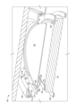


Classifications
-
- H—ELECTRICITY
- H10—SEMICONDUCTOR DEVICES; ELECTRIC SOLID-STATE DEVICES NOT OTHERWISE PROVIDED FOR
- H10P—GENERIC PROCESSES OR APPARATUS FOR THE MANUFACTURE OR TREATMENT OF DEVICES COVERED BY CLASS H10
- H10P72/00—Handling or holding of wafers, substrates or devices during manufacture or treatment thereof
- H10P72/70—Handling or holding of wafers, substrates or devices during manufacture or treatment thereof for supporting or gripping
- H10P72/76—Handling or holding of wafers, substrates or devices during manufacture or treatment thereof for supporting or gripping using mechanical means, e.g. clamps or pinches
- H10P72/7604—Handling or holding of wafers, substrates or devices during manufacture or treatment thereof for supporting or gripping using mechanical means, e.g. clamps or pinches the wafers being placed on a susceptor, stage or support
- H10P72/7606—Handling or holding of wafers, substrates or devices during manufacture or treatment thereof for supporting or gripping using mechanical means, e.g. clamps or pinches the wafers being placed on a susceptor, stage or support characterised by edge clamping, e.g. clamping ring
-
- C—CHEMISTRY; METALLURGY
- C23—COATING METALLIC MATERIAL; COATING MATERIAL WITH METALLIC MATERIAL; CHEMICAL SURFACE TREATMENT; DIFFUSION TREATMENT OF METALLIC MATERIAL; COATING BY VACUUM EVAPORATION, BY SPUTTERING, BY ION IMPLANTATION OR BY CHEMICAL VAPOUR DEPOSITION, IN GENERAL; INHIBITING CORROSION OF METALLIC MATERIAL OR INCRUSTATION IN GENERAL
- C23C—COATING METALLIC MATERIAL; COATING MATERIAL WITH METALLIC MATERIAL; SURFACE TREATMENT OF METALLIC MATERIAL BY DIFFUSION INTO THE SURFACE, BY CHEMICAL CONVERSION OR SUBSTITUTION; COATING BY VACUUM EVAPORATION, BY SPUTTERING, BY ION IMPLANTATION OR BY CHEMICAL VAPOUR DEPOSITION, IN GENERAL
- C23C14/00—Coating by vacuum evaporation, by sputtering or by ion implantation of the coating forming material
- C23C14/22—Coating by vacuum evaporation, by sputtering or by ion implantation of the coating forming material characterised by the process of coating
- C23C14/34—Sputtering
- C23C14/3435—Applying energy to the substrate during sputtering
- C23C14/345—Applying energy to the substrate during sputtering using substrate bias
-
- C—CHEMISTRY; METALLURGY
- C23—COATING METALLIC MATERIAL; COATING MATERIAL WITH METALLIC MATERIAL; CHEMICAL SURFACE TREATMENT; DIFFUSION TREATMENT OF METALLIC MATERIAL; COATING BY VACUUM EVAPORATION, BY SPUTTERING, BY ION IMPLANTATION OR BY CHEMICAL VAPOUR DEPOSITION, IN GENERAL; INHIBITING CORROSION OF METALLIC MATERIAL OR INCRUSTATION IN GENERAL
- C23C—COATING METALLIC MATERIAL; COATING MATERIAL WITH METALLIC MATERIAL; SURFACE TREATMENT OF METALLIC MATERIAL BY DIFFUSION INTO THE SURFACE, BY CHEMICAL CONVERSION OR SUBSTITUTION; COATING BY VACUUM EVAPORATION, BY SPUTTERING, BY ION IMPLANTATION OR BY CHEMICAL VAPOUR DEPOSITION, IN GENERAL
- C23C14/00—Coating by vacuum evaporation, by sputtering or by ion implantation of the coating forming material
- C23C14/22—Coating by vacuum evaporation, by sputtering or by ion implantation of the coating forming material characterised by the process of coating
- C23C14/34—Sputtering
- C23C14/35—Sputtering by application of a magnetic field, e.g. magnetron sputtering
- C23C14/351—Sputtering by application of a magnetic field, e.g. magnetron sputtering using a magnetic field in close vicinity to the substrate
-
- C—CHEMISTRY; METALLURGY
- C23—COATING METALLIC MATERIAL; COATING MATERIAL WITH METALLIC MATERIAL; CHEMICAL SURFACE TREATMENT; DIFFUSION TREATMENT OF METALLIC MATERIAL; COATING BY VACUUM EVAPORATION, BY SPUTTERING, BY ION IMPLANTATION OR BY CHEMICAL VAPOUR DEPOSITION, IN GENERAL; INHIBITING CORROSION OF METALLIC MATERIAL OR INCRUSTATION IN GENERAL
- C23C—COATING METALLIC MATERIAL; COATING MATERIAL WITH METALLIC MATERIAL; SURFACE TREATMENT OF METALLIC MATERIAL BY DIFFUSION INTO THE SURFACE, BY CHEMICAL CONVERSION OR SUBSTITUTION; COATING BY VACUUM EVAPORATION, BY SPUTTERING, BY ION IMPLANTATION OR BY CHEMICAL VAPOUR DEPOSITION, IN GENERAL
- C23C14/00—Coating by vacuum evaporation, by sputtering or by ion implantation of the coating forming material
- C23C14/22—Coating by vacuum evaporation, by sputtering or by ion implantation of the coating forming material characterised by the process of coating
- C23C14/50—Substrate holders
-
- C—CHEMISTRY; METALLURGY
- C23—COATING METALLIC MATERIAL; COATING MATERIAL WITH METALLIC MATERIAL; CHEMICAL SURFACE TREATMENT; DIFFUSION TREATMENT OF METALLIC MATERIAL; COATING BY VACUUM EVAPORATION, BY SPUTTERING, BY ION IMPLANTATION OR BY CHEMICAL VAPOUR DEPOSITION, IN GENERAL; INHIBITING CORROSION OF METALLIC MATERIAL OR INCRUSTATION IN GENERAL
- C23C—COATING METALLIC MATERIAL; COATING MATERIAL WITH METALLIC MATERIAL; SURFACE TREATMENT OF METALLIC MATERIAL BY DIFFUSION INTO THE SURFACE, BY CHEMICAL CONVERSION OR SUBSTITUTION; COATING BY VACUUM EVAPORATION, BY SPUTTERING, BY ION IMPLANTATION OR BY CHEMICAL VAPOUR DEPOSITION, IN GENERAL
- C23C16/00—Chemical coating by decomposition of gaseous compounds, without leaving reaction products of surface material in the coating, i.e. chemical vapour deposition [CVD] processes
- C23C16/44—Chemical coating by decomposition of gaseous compounds, without leaving reaction products of surface material in the coating, i.e. chemical vapour deposition [CVD] processes characterised by the method of coating
- C23C16/455—Chemical coating by decomposition of gaseous compounds, without leaving reaction products of surface material in the coating, i.e. chemical vapour deposition [CVD] processes characterised by the method of coating characterised by the method used for introducing gases into reaction chamber or for modifying gas flows in reaction chamber
- C23C16/45523—Pulsed gas flow or change of composition over time
- C23C16/45525—Atomic layer deposition [ALD]
- C23C16/45527—Atomic layer deposition [ALD] characterized by the ALD cycle, e.g. different flows or temperatures during half-reactions, unusual pulsing sequence, use of precursor mixtures or auxiliary reactants or activations
- C23C16/45536—Use of plasma, radiation or electromagnetic fields
-
- C—CHEMISTRY; METALLURGY
- C23—COATING METALLIC MATERIAL; COATING MATERIAL WITH METALLIC MATERIAL; CHEMICAL SURFACE TREATMENT; DIFFUSION TREATMENT OF METALLIC MATERIAL; COATING BY VACUUM EVAPORATION, BY SPUTTERING, BY ION IMPLANTATION OR BY CHEMICAL VAPOUR DEPOSITION, IN GENERAL; INHIBITING CORROSION OF METALLIC MATERIAL OR INCRUSTATION IN GENERAL
- C23C—COATING METALLIC MATERIAL; COATING MATERIAL WITH METALLIC MATERIAL; SURFACE TREATMENT OF METALLIC MATERIAL BY DIFFUSION INTO THE SURFACE, BY CHEMICAL CONVERSION OR SUBSTITUTION; COATING BY VACUUM EVAPORATION, BY SPUTTERING, BY ION IMPLANTATION OR BY CHEMICAL VAPOUR DEPOSITION, IN GENERAL
- C23C16/00—Chemical coating by decomposition of gaseous compounds, without leaving reaction products of surface material in the coating, i.e. chemical vapour deposition [CVD] processes
- C23C16/44—Chemical coating by decomposition of gaseous compounds, without leaving reaction products of surface material in the coating, i.e. chemical vapour deposition [CVD] processes characterised by the method of coating
- C23C16/458—Chemical coating by decomposition of gaseous compounds, without leaving reaction products of surface material in the coating, i.e. chemical vapour deposition [CVD] processes characterised by the method of coating characterised by the method used for supporting substrates in the reaction chamber
- C23C16/4582—Rigid and flat substrates, e.g. plates or discs
-
- C—CHEMISTRY; METALLURGY
- C23—COATING METALLIC MATERIAL; COATING MATERIAL WITH METALLIC MATERIAL; CHEMICAL SURFACE TREATMENT; DIFFUSION TREATMENT OF METALLIC MATERIAL; COATING BY VACUUM EVAPORATION, BY SPUTTERING, BY ION IMPLANTATION OR BY CHEMICAL VAPOUR DEPOSITION, IN GENERAL; INHIBITING CORROSION OF METALLIC MATERIAL OR INCRUSTATION IN GENERAL
- C23C—COATING METALLIC MATERIAL; COATING MATERIAL WITH METALLIC MATERIAL; SURFACE TREATMENT OF METALLIC MATERIAL BY DIFFUSION INTO THE SURFACE, BY CHEMICAL CONVERSION OR SUBSTITUTION; COATING BY VACUUM EVAPORATION, BY SPUTTERING, BY ION IMPLANTATION OR BY CHEMICAL VAPOUR DEPOSITION, IN GENERAL
- C23C16/00—Chemical coating by decomposition of gaseous compounds, without leaving reaction products of surface material in the coating, i.e. chemical vapour deposition [CVD] processes
- C23C16/44—Chemical coating by decomposition of gaseous compounds, without leaving reaction products of surface material in the coating, i.e. chemical vapour deposition [CVD] processes characterised by the method of coating
- C23C16/458—Chemical coating by decomposition of gaseous compounds, without leaving reaction products of surface material in the coating, i.e. chemical vapour deposition [CVD] processes characterised by the method of coating characterised by the method used for supporting substrates in the reaction chamber
- C23C16/4582—Rigid and flat substrates, e.g. plates or discs
- C23C16/4583—Rigid and flat substrates, e.g. plates or discs the substrate being supported substantially horizontally
- C23C16/4585—Devices at or outside the perimeter of the substrate support, e.g. clamping rings, shrouds
-
- H—ELECTRICITY
- H01—ELECTRIC ELEMENTS
- H01J—ELECTRIC DISCHARGE TUBES OR DISCHARGE LAMPS
- H01J37/00—Discharge tubes with provision for introducing objects or material to be exposed to the discharge, e.g. for the purpose of examination or processing thereof
- H01J37/32—Gas-filled discharge tubes
- H01J37/32431—Constructional details of the reactor
- H01J37/32623—Mechanical discharge control means
- H01J37/32642—Focus rings
-
- H—ELECTRICITY
- H01—ELECTRIC ELEMENTS
- H01J—ELECTRIC DISCHARGE TUBES OR DISCHARGE LAMPS
- H01J37/00—Discharge tubes with provision for introducing objects or material to be exposed to the discharge, e.g. for the purpose of examination or processing thereof
- H01J37/32—Gas-filled discharge tubes
- H01J37/32431—Constructional details of the reactor
- H01J37/32623—Mechanical discharge control means
- H01J37/32651—Shields, e.g. dark space shields, Faraday shields
-
- H—ELECTRICITY
- H01—ELECTRIC ELEMENTS
- H01J—ELECTRIC DISCHARGE TUBES OR DISCHARGE LAMPS
- H01J37/00—Discharge tubes with provision for introducing objects or material to be exposed to the discharge, e.g. for the purpose of examination or processing thereof
- H01J37/32—Gas-filled discharge tubes
- H01J37/32431—Constructional details of the reactor
- H01J37/32715—Workpiece holder
-
- H—ELECTRICITY
- H10—SEMICONDUCTOR DEVICES; ELECTRIC SOLID-STATE DEVICES NOT OTHERWISE PROVIDED FOR
- H10P—GENERIC PROCESSES OR APPARATUS FOR THE MANUFACTURE OR TREATMENT OF DEVICES COVERED BY CLASS H10
- H10P14/00—Formation of materials, e.g. in the shape of layers or pillars
- H10P14/20—Formation of materials, e.g. in the shape of layers or pillars of semiconductor materials
-
- H—ELECTRICITY
- H10—SEMICONDUCTOR DEVICES; ELECTRIC SOLID-STATE DEVICES NOT OTHERWISE PROVIDED FOR
- H10P—GENERIC PROCESSES OR APPARATUS FOR THE MANUFACTURE OR TREATMENT OF DEVICES COVERED BY CLASS H10
- H10P72/00—Handling or holding of wafers, substrates or devices during manufacture or treatment thereof
- H10P72/04—Apparatus for manufacture or treatment
- H10P72/0402—Apparatus for fluid treatment
-
- H—ELECTRICITY
- H10—SEMICONDUCTOR DEVICES; ELECTRIC SOLID-STATE DEVICES NOT OTHERWISE PROVIDED FOR
- H10P—GENERIC PROCESSES OR APPARATUS FOR THE MANUFACTURE OR TREATMENT OF DEVICES COVERED BY CLASS H10
- H10P72/00—Handling or holding of wafers, substrates or devices during manufacture or treatment thereof
- H10P72/70—Handling or holding of wafers, substrates or devices during manufacture or treatment thereof for supporting or gripping
- H10P72/72—Handling or holding of wafers, substrates or devices during manufacture or treatment thereof for supporting or gripping using electrostatic chucks
-
- H—ELECTRICITY
- H10—SEMICONDUCTOR DEVICES; ELECTRIC SOLID-STATE DEVICES NOT OTHERWISE PROVIDED FOR
- H10P—GENERIC PROCESSES OR APPARATUS FOR THE MANUFACTURE OR TREATMENT OF DEVICES COVERED BY CLASS H10
- H10P72/00—Handling or holding of wafers, substrates or devices during manufacture or treatment thereof
- H10P72/70—Handling or holding of wafers, substrates or devices during manufacture or treatment thereof for supporting or gripping
- H10P72/72—Handling or holding of wafers, substrates or devices during manufacture or treatment thereof for supporting or gripping using electrostatic chucks
- H10P72/722—Details of electrostatic chucks
-
- H—ELECTRICITY
- H10—SEMICONDUCTOR DEVICES; ELECTRIC SOLID-STATE DEVICES NOT OTHERWISE PROVIDED FOR
- H10P—GENERIC PROCESSES OR APPARATUS FOR THE MANUFACTURE OR TREATMENT OF DEVICES COVERED BY CLASS H10
- H10P72/00—Handling or holding of wafers, substrates or devices during manufacture or treatment thereof
- H10P72/70—Handling or holding of wafers, substrates or devices during manufacture or treatment thereof for supporting or gripping
- H10P72/76—Handling or holding of wafers, substrates or devices during manufacture or treatment thereof for supporting or gripping using mechanical means, e.g. clamps or pinches
- H10P72/7604—Handling or holding of wafers, substrates or devices during manufacture or treatment thereof for supporting or gripping using mechanical means, e.g. clamps or pinches the wafers being placed on a susceptor, stage or support
- H10P72/7612—Handling or holding of wafers, substrates or devices during manufacture or treatment thereof for supporting or gripping using mechanical means, e.g. clamps or pinches the wafers being placed on a susceptor, stage or support characterised by lifting arrangements, e.g. lift pins
-
- H—ELECTRICITY
- H10—SEMICONDUCTOR DEVICES; ELECTRIC SOLID-STATE DEVICES NOT OTHERWISE PROVIDED FOR
- H10P—GENERIC PROCESSES OR APPARATUS FOR THE MANUFACTURE OR TREATMENT OF DEVICES COVERED BY CLASS H10
- H10P72/00—Handling or holding of wafers, substrates or devices during manufacture or treatment thereof
- H10P72/70—Handling or holding of wafers, substrates or devices during manufacture or treatment thereof for supporting or gripping
- H10P72/76—Handling or holding of wafers, substrates or devices during manufacture or treatment thereof for supporting or gripping using mechanical means, e.g. clamps or pinches
- H10P72/7604—Handling or holding of wafers, substrates or devices during manufacture or treatment thereof for supporting or gripping using mechanical means, e.g. clamps or pinches the wafers being placed on a susceptor, stage or support
- H10P72/7614—Handling or holding of wafers, substrates or devices during manufacture or treatment thereof for supporting or gripping using mechanical means, e.g. clamps or pinches the wafers being placed on a susceptor, stage or support characterised by a plurality of individual support members, e.g. support posts or protrusions
Landscapes
- Chemical & Material Sciences (AREA)
- Engineering & Computer Science (AREA)
- Chemical Kinetics & Catalysis (AREA)
- Materials Engineering (AREA)
- Mechanical Engineering (AREA)
- Metallurgy (AREA)
- Organic Chemistry (AREA)
- Physics & Mathematics (AREA)
- Plasma & Fusion (AREA)
- General Chemical & Material Sciences (AREA)
- Analytical Chemistry (AREA)
- Electromagnetism (AREA)
- Power Engineering (AREA)
- Chemical Vapour Deposition (AREA)
- Container, Conveyance, Adherence, Positioning, Of Wafer (AREA)
- Drying Of Semiconductors (AREA)
- Physical Vapour Deposition (AREA)
- Gasket Seals (AREA)
Applications Claiming Priority (3)
| Application Number | Priority Date | Filing Date | Title |
|---|---|---|---|
| US16/951,823 US11996315B2 (en) | 2020-11-18 | 2020-11-18 | Thin substrate handling via edge clamping |
| US16/951,823 | 2020-11-18 | ||
| PCT/US2021/059404 WO2022108879A1 (en) | 2020-11-18 | 2021-11-15 | Thin substrate handling via edge clamping |
Publications (2)
| Publication Number | Publication Date |
|---|---|
| JP2023549527A true JP2023549527A (ja) | 2023-11-27 |
| JP2023549527A5 JP2023549527A5 (https=) | 2024-11-22 |
Family
ID=81587901
Family Applications (1)
| Application Number | Title | Priority Date | Filing Date |
|---|---|---|---|
| JP2023528612A Pending JP2023549527A (ja) | 2020-11-18 | 2021-11-15 | エッジクランプによる薄型基板ハンドリング |
Country Status (5)
| Country | Link |
|---|---|
| US (1) | US11996315B2 (https=) |
| JP (1) | JP2023549527A (https=) |
| CN (1) | CN116711060A (https=) |
| TW (1) | TWI910268B (https=) |
| WO (1) | WO2022108879A1 (https=) |
Families Citing this family (5)
| Publication number | Priority date | Publication date | Assignee | Title |
|---|---|---|---|---|
| US11935728B2 (en) * | 2020-01-31 | 2024-03-19 | Taiwan Semiconductor Manufacturing Company, Ltd. | Apparatus and method of manufacturing a semiconductor device |
| US11996315B2 (en) * | 2020-11-18 | 2024-05-28 | Applied Materials, Inc. | Thin substrate handling via edge clamping |
| USD1038049S1 (en) | 2020-11-18 | 2024-08-06 | Applied Materials, Inc. | Cover ring for use in semiconductor processing chamber |
| US12371790B2 (en) * | 2022-08-17 | 2025-07-29 | Sky Tech Inc. | Wafer carrier with adjustable alignment devices and deposition equipment using the same |
| US20240186176A1 (en) * | 2022-12-02 | 2024-06-06 | Onto Innovation Inc. | Stage actuator particle shield |
Citations (2)
| Publication number | Priority date | Publication date | Assignee | Title |
|---|---|---|---|---|
| US5632873A (en) * | 1995-05-22 | 1997-05-27 | Stevens; Joseph J. | Two piece anti-stick clamp ring |
| JP2011518255A (ja) * | 2008-04-16 | 2011-06-23 | アプライド マテリアルズ インコーポレイテッド | ウェハ処理堆積物遮蔽構成材 |
Family Cites Families (34)
| Publication number | Priority date | Publication date | Assignee | Title |
|---|---|---|---|---|
| US5524905A (en) | 1994-09-28 | 1996-06-11 | Greene, Tweed Of Delaware, Inc. | Sealing assembly with T-shaped seal ring and anti-extrusion rings |
| US5632673A (en) | 1995-10-30 | 1997-05-27 | Chrysler Corporation | Ventilation system for lightweight automobile |
| US5810931A (en) * | 1996-07-30 | 1998-09-22 | Applied Materials, Inc. | High aspect ratio clamp ring |
| US6051122A (en) * | 1997-08-21 | 2000-04-18 | Applied Materials, Inc. | Deposition shield assembly for a semiconductor wafer processing system |
| US6123804A (en) * | 1999-02-22 | 2000-09-26 | Applied Materials, Inc. | Sectional clamp ring |
| US6162336A (en) * | 1999-07-12 | 2000-12-19 | Chartered Semiconductor Manufacturing Ltd. | Clamping ring design to reduce wafer sticking problem in metal deposition |
| US20040149226A1 (en) * | 2003-01-30 | 2004-08-05 | Taiwan Semiconductor Manufacturing Co., Ltd. | Substrate clamp ring with removable contract pads |
| JP2005333063A (ja) * | 2004-05-21 | 2005-12-02 | Renesas Technology Corp | クランプ部材、成膜装置、成膜方法、半導体装置の製造方法 |
| JP3887394B2 (ja) * | 2004-10-08 | 2007-02-28 | 芝浦メカトロニクス株式会社 | 脆性材料の割断加工システム及びその方法 |
| USD559993S1 (en) | 2005-03-30 | 2008-01-15 | Tokyo Electron Limited | Cover ring |
| TWD121115S1 (zh) | 2005-03-30 | 2008-01-21 | 東京威力科創股份有限公司 | 遮護環 |
| DE102005032547B4 (de) * | 2005-07-12 | 2010-01-07 | Texas Instruments Deutschland Gmbh | Wafer-Klemmanordnung zur Aufnahme eines Wafers während eines Abscheidungsverfahrens |
| USD557226S1 (en) | 2005-08-25 | 2007-12-11 | Hitachi High-Technologies Corporation | Electrode cover for a plasma processing apparatus |
| US7520969B2 (en) | 2006-03-07 | 2009-04-21 | Applied Materials, Inc. | Notched deposition ring |
| US20070283884A1 (en) * | 2006-05-30 | 2007-12-13 | Applied Materials, Inc. | Ring assembly for substrate processing chamber |
| US7981262B2 (en) | 2007-01-29 | 2011-07-19 | Applied Materials, Inc. | Process kit for substrate processing chamber |
| US9490166B2 (en) * | 2010-12-08 | 2016-11-08 | Evatec Ag | Apparatus and method for depositing a layer onto a substrate |
| JP6056403B2 (ja) * | 2012-11-15 | 2017-01-11 | 東京エレクトロン株式会社 | 成膜装置 |
| US9472443B2 (en) | 2013-03-14 | 2016-10-18 | Applied Materials, Inc. | Selectively groundable cover ring for substrate process chambers |
| JP1494712S (https=) | 2013-05-15 | 2017-04-03 | ||
| TWD161030S (zh) | 2013-08-12 | 2014-06-11 | 陳世發 | 基板保持環 |
| CN104862660B (zh) * | 2014-02-24 | 2017-10-13 | 北京北方华创微电子装备有限公司 | 承载装置及等离子体加工设备 |
| US9343343B2 (en) | 2014-05-19 | 2016-05-17 | Asm Ip Holding B.V. | Method for reducing particle generation at bevel portion of substrate |
| USD797691S1 (en) | 2016-04-14 | 2017-09-19 | Applied Materials, Inc. | Composite edge ring |
| JP1584906S (https=) | 2017-01-31 | 2017-08-28 | ||
| JP1584241S (https=) | 2017-01-31 | 2017-08-21 | ||
| JP1598998S (https=) | 2017-08-31 | 2018-03-05 | ||
| USD888903S1 (en) | 2018-12-17 | 2020-06-30 | Applied Materials, Inc. | Deposition ring for physical vapor deposition chamber |
| KR102305539B1 (ko) | 2019-04-16 | 2021-09-27 | 주식회사 티씨케이 | SiC 엣지 링 |
| KR102277809B1 (ko) | 2019-07-15 | 2021-07-14 | 세메스 주식회사 | 기판 지지 유닛 및 이를 구비하는 기판 처리 시스템 |
| JP1659287S (https=) | 2019-10-18 | 2020-05-11 | ||
| USD934315S1 (en) | 2020-03-20 | 2021-10-26 | Applied Materials, Inc. | Deposition ring for a substrate processing chamber |
| US12100579B2 (en) * | 2020-11-18 | 2024-09-24 | Applied Materials, Inc. | Deposition ring for thin substrate handling via edge clamping |
| US11996315B2 (en) * | 2020-11-18 | 2024-05-28 | Applied Materials, Inc. | Thin substrate handling via edge clamping |
-
2020
- 2020-11-18 US US16/951,823 patent/US11996315B2/en active Active
-
2021
- 2021-11-15 CN CN202180080408.2A patent/CN116711060A/zh active Pending
- 2021-11-15 JP JP2023528612A patent/JP2023549527A/ja active Pending
- 2021-11-15 WO PCT/US2021/059404 patent/WO2022108879A1/en not_active Ceased
- 2021-11-17 TW TW110142710A patent/TWI910268B/zh active
Patent Citations (2)
| Publication number | Priority date | Publication date | Assignee | Title |
|---|---|---|---|---|
| US5632873A (en) * | 1995-05-22 | 1997-05-27 | Stevens; Joseph J. | Two piece anti-stick clamp ring |
| JP2011518255A (ja) * | 2008-04-16 | 2011-06-23 | アプライド マテリアルズ インコーポレイテッド | ウェハ処理堆積物遮蔽構成材 |
Also Published As
| Publication number | Publication date |
|---|---|
| TWI910268B (zh) | 2026-01-01 |
| TW202224067A (zh) | 2022-06-16 |
| US11996315B2 (en) | 2024-05-28 |
| WO2022108879A1 (en) | 2022-05-27 |
| CN116711060A (zh) | 2023-09-05 |
| KR20230123473A (ko) | 2023-08-23 |
| US20220157635A1 (en) | 2022-05-19 |
Similar Documents
| Publication | Publication Date | Title |
|---|---|---|
| US12100579B2 (en) | Deposition ring for thin substrate handling via edge clamping | |
| JP2023549527A (ja) | エッジクランプによる薄型基板ハンドリング | |
| TWI744417B (zh) | 具有浮動遮蔽環的製程套件 | |
| US12014906B2 (en) | High temperature detachable very high frequency (VHF) electrostatic chuck (ESC) for PVD chamber | |
| TWI870447B (zh) | 用於處理腔室的高導通下部護罩 | |
| JP7499876B2 (ja) | シャワーヘッドを有する事前洗浄チャンバ上側シールド | |
| US12183560B2 (en) | Gas injection process kit to eliminate arcing and improve uniform gas distribution for a PVD process | |
| KR102489441B1 (ko) | 키트 수명을 개선하기 위한 고 압축 응력 막 증착을 위한 장치 | |
| CN117581327A (zh) | 用于改良的高压等离子体处理的设备 | |
| TW202443782A (zh) | 壽命延長的靜電夾盤 | |
| KR102959528B1 (ko) | 에지 클램핑을 통한 얇은 기판 처리 | |
| TWI915451B (zh) | 使用用於經由邊緣夾鉗進行薄基板操縱的沉積環的處理套組、處理腔室及方法 | |
| US20260015712A1 (en) | Detachable Mid Temp Electrostatic Chuck (ESC) for Process Chamber | |
| CN114930492A (zh) | 用于rf腔室的改进阳极-阴极比例的设备 | |
| TW202301411A (zh) | 將處理環境擴展到基板直徑之外的基板邊緣環 |
Legal Events
| Date | Code | Title | Description |
|---|---|---|---|
| A521 | Request for written amendment filed |
Free format text: JAPANESE INTERMEDIATE CODE: A523 Effective date: 20241114 |
|
| A621 | Written request for application examination |
Free format text: JAPANESE INTERMEDIATE CODE: A621 Effective date: 20241114 |
|
| A977 | Report on retrieval |
Free format text: JAPANESE INTERMEDIATE CODE: A971007 Effective date: 20251114 |
|
| A131 | Notification of reasons for refusal |
Free format text: JAPANESE INTERMEDIATE CODE: A131 Effective date: 20251223 |