JP2023166322A - 導波路構造およびそれを用いた表示装置 - Google Patents
導波路構造およびそれを用いた表示装置 Download PDFInfo
- Publication number
- JP2023166322A JP2023166322A JP2022169058A JP2022169058A JP2023166322A JP 2023166322 A JP2023166322 A JP 2023166322A JP 2022169058 A JP2022169058 A JP 2022169058A JP 2022169058 A JP2022169058 A JP 2022169058A JP 2023166322 A JP2023166322 A JP 2023166322A
- Authority
- JP
- Japan
- Prior art keywords
- waveguide
- grating
- pillar
- coupler
- refractive index
- Prior art date
- Legal status (The legal status is an assumption and is not a legal conclusion. Google has not performed a legal analysis and makes no representation as to the accuracy of the status listed.)
- Granted
Links
Images


Classifications
-
- G—PHYSICS
- G02—OPTICS
- G02B—OPTICAL ELEMENTS, SYSTEMS OR APPARATUS
- G02B6/00—Light guides; Structural details of arrangements comprising light guides and other optical elements, e.g. couplings
- G02B6/10—Light guides; Structural details of arrangements comprising light guides and other optical elements, e.g. couplings of the optical waveguide type
-
- G—PHYSICS
- G02—OPTICS
- G02B—OPTICAL ELEMENTS, SYSTEMS OR APPARATUS
- G02B5/00—Optical elements other than lenses
- G02B5/18—Diffraction gratings
- G02B5/1866—Transmission gratings characterised by their structure, e.g. step profile, contours of substrate or grooves, pitch variations, materials
-
- G—PHYSICS
- G02—OPTICS
- G02B—OPTICAL ELEMENTS, SYSTEMS OR APPARATUS
- G02B6/00—Light guides; Structural details of arrangements comprising light guides and other optical elements, e.g. couplings
- G02B6/10—Light guides; Structural details of arrangements comprising light guides and other optical elements, e.g. couplings of the optical waveguide type
- G02B6/12—Light guides; Structural details of arrangements comprising light guides and other optical elements, e.g. couplings of the optical waveguide type of the integrated circuit kind
- G02B6/122—Basic optical elements, e.g. light-guiding paths
- G02B6/125—Bends, branchings or intersections
-
- G—PHYSICS
- G02—OPTICS
- G02B—OPTICAL ELEMENTS, SYSTEMS OR APPARATUS
- G02B27/00—Optical systems or apparatus not provided for by any of the groups G02B1/00 - G02B26/00, G02B30/00
- G02B27/01—Head-up displays
- G02B27/017—Head mounted
- G02B27/0172—Head mounted characterised by optical features
-
- G—PHYSICS
- G02—OPTICS
- G02B—OPTICAL ELEMENTS, SYSTEMS OR APPARATUS
- G02B27/00—Optical systems or apparatus not provided for by any of the groups G02B1/00 - G02B26/00, G02B30/00
- G02B27/01—Head-up displays
- G02B27/0101—Head-up displays characterised by optical features
-
- G—PHYSICS
- G02—OPTICS
- G02B—OPTICAL ELEMENTS, SYSTEMS OR APPARATUS
- G02B27/00—Optical systems or apparatus not provided for by any of the groups G02B1/00 - G02B26/00, G02B30/00
- G02B27/30—Collimators
-
- G—PHYSICS
- G02—OPTICS
- G02B—OPTICAL ELEMENTS, SYSTEMS OR APPARATUS
- G02B5/00—Optical elements other than lenses
- G02B5/18—Diffraction gratings
- G02B5/1814—Diffraction gratings structurally combined with one or more further optical elements, e.g. lenses, mirrors, prisms or other diffraction gratings
- G02B5/1819—Plural gratings positioned on the same surface, e.g. array of gratings
-
- G—PHYSICS
- G02—OPTICS
- G02B—OPTICAL ELEMENTS, SYSTEMS OR APPARATUS
- G02B5/00—Optical elements other than lenses
- G02B5/18—Diffraction gratings
- G02B5/1842—Gratings for image generation
-
- G—PHYSICS
- G02—OPTICS
- G02B—OPTICAL ELEMENTS, SYSTEMS OR APPARATUS
- G02B5/00—Optical elements other than lenses
- G02B5/18—Diffraction gratings
- G02B5/1866—Transmission gratings characterised by their structure, e.g. step profile, contours of substrate or grooves, pitch variations, materials
- G02B5/1871—Transmissive phase gratings
-
- G—PHYSICS
- G02—OPTICS
- G02B—OPTICAL ELEMENTS, SYSTEMS OR APPARATUS
- G02B6/00—Light guides; Structural details of arrangements comprising light guides and other optical elements, e.g. couplings
- G02B6/0001—Light guides; Structural details of arrangements comprising light guides and other optical elements, e.g. couplings specially adapted for lighting devices or systems
- G02B6/0011—Light guides; Structural details of arrangements comprising light guides and other optical elements, e.g. couplings specially adapted for lighting devices or systems the light guides being planar or of plate-like form
- G02B6/0013—Means for improving the coupling-in of light from the light source into the light guide
- G02B6/0023—Means for improving the coupling-in of light from the light source into the light guide provided by one optical element, or plurality thereof, placed between the light guide and the light source, or around the light source
- G02B6/0026—Wavelength selective element, sheet or layer, e.g. filter or grating
-
- G—PHYSICS
- G02—OPTICS
- G02B—OPTICAL ELEMENTS, SYSTEMS OR APPARATUS
- G02B6/00—Light guides; Structural details of arrangements comprising light guides and other optical elements, e.g. couplings
- G02B6/10—Light guides; Structural details of arrangements comprising light guides and other optical elements, e.g. couplings of the optical waveguide type
- G02B6/12—Light guides; Structural details of arrangements comprising light guides and other optical elements, e.g. couplings of the optical waveguide type of the integrated circuit kind
- G02B2006/12083—Constructional arrangements
- G02B2006/12092—Stepped
-
- G—PHYSICS
- G02—OPTICS
- G02B—OPTICAL ELEMENTS, SYSTEMS OR APPARATUS
- G02B27/00—Optical systems or apparatus not provided for by any of the groups G02B1/00 - G02B26/00, G02B30/00
- G02B27/01—Head-up displays
- G02B27/0101—Head-up displays characterised by optical features
- G02B2027/0123—Head-up displays characterised by optical features comprising devices increasing the field of view
Landscapes
- Physics & Mathematics (AREA)
- General Physics & Mathematics (AREA)
- Optics & Photonics (AREA)
- Engineering & Computer Science (AREA)
- Microelectronics & Electronic Packaging (AREA)
- Optical Couplings Of Light Guides (AREA)
- Diffracting Gratings Or Hologram Optical Elements (AREA)
- Optical Integrated Circuits (AREA)
Abstract

【課題】 導波路構造およびそれを用いた表示装置を提供する。
【解決手段】 互いに積層された導波路結合器を含み、各前記導波路結合器は、導波路板、および前記導波路板上に配置された入力カプラを含み、少なくとも1つの前記導波路結合器の前記入力カプラは第1のグレーティングピラーを含み、各前記第1のグレーティングピラーは徐々に変化する屈折率を有する導波路構造。
【選択図】 図1
Description
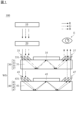
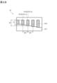
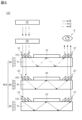
10 画像ソース
20 コリメータ
30、40、50 導波路結合器
31、351、41、51 導波路板
33、43、53 入力カプラ
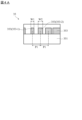
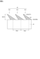
331、353、353-1、353-2、431、531 グレーティングピラー
35、45、55 エキスパンダー
37、47、57 出力カプラ
B 青色光
E 目
G 緑色光
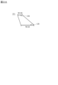
H331、H431 全高
LB 下底
LS 下辺
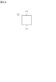
P1、P33、P43 周期
R 赤色光
S1、S1B、S1T、S2、S2B、S2T 積層
T1、T2 厚さ
UB 上底
US 上辺
W1、W2 幅
WS 導波路構造
WLB 下底LBの幅
WUB 上底UBの幅
Claims (10)
- 互いに積層された導波路結合器を含み、
各前記導波路結合器は、
導波路板、および
前記導波路板上に配置された入力カプラを含み、
少なくとも1つの前記導波路結合器の前記入力カプラは第1のグレーティングピラーを含み、
各前記第1のグレーティングピラーは徐々に変化する屈折率を有する導波路構造。 - 前記導波路結合器の数は、2つ以上の導波路結合器であり、
前記導波路結合器は、異なる色の光を結合するように用いられ、
前記異なる色の光は、380nm~750nmの波長を有する請求項1に記載の導波路構造。 - 各前記第1のグレーティングピラーは積層を有し、
前記積層の数は2以上、30以下であり、
前記積層の全高は、40nm~1000nmの範囲にある請求項1に記載の導波路構造。 - 前記徐々に変化する屈折率は、最大屈折率および最小屈折率を有し、
前記最大屈折率と前記最小屈折率との差は0より大きく、2.1以下であり、
前記徐々に変化する屈折率は、1.4~3.5の範囲にあり、
前記導波路板は、1.5~3.0の範囲で一定の屈折率を有する請求項1に記載の導波路構造。 - 前記第1のグレーティングピラーは周期的な配列で形成され、
前記周期的な配列の周期は、250nm~750nmの範囲にある請求項1に記載の導波路構造。 - 前記導波路構造の断面図から見て、各前記第1のグレーティングピラーのプロファイルは、2つの平行な辺を有し、各前記第1のグレーティングピラーの前記プロファイルは台形であり、前記2つの平行な辺は、上底および下底であり、前記下底は前記上底より前記導波路板に近く、前記下底は前記上底より長い請求項1に記載の導波路構造。
- 各前記導波路結合器は、
前記導波路板上に配置され、前記入力カプラに隣接するエキスパンダーをさらに含み、
前記エキスパンダーは第2のグレーティングピラーを含み、
2つの隣接する第2のグレーティングピラー間の距離は一定である請求項1に記載の導波路構造。 - 各前記導波路結合器は、前記導波路板上に配置された出力カプラをさらに含み、
前記エキスパンダーは、前記入力カプラと前記出力カプラとの間に配置される請求項7に記載の導波路構造。 - 画像ソース、および
前記画像ソースからの光を結合するように構成された導波路構造を含み、
前記導波路構造は、互いに積層された導波路結合器を含み、
各前記導波路結合器は、導波路板、および前記導波路板上に配置された入力カプラを含み、
少なくとも1つの前記導波路結合器の前記入力カプラは、第1のグレーティングピラーを含み、各前記第1のグレーティングピラーは徐々に変化する屈折率を有する表示装置。 - 前記画像ソースと前記導波路構造との間に配置されたコリメータをさらに含む請求項9に記載の表示装置。
Applications Claiming Priority (2)
| Application Number | Priority Date | Filing Date | Title |
|---|---|---|---|
| US17/739,888 | 2022-05-09 | ||
| US17/739,888 US20230359031A1 (en) | 2022-05-09 | 2022-05-09 | Waveguide structure and display device using the same |
Publications (2)
| Publication Number | Publication Date |
|---|---|
| JP2023166322A true JP2023166322A (ja) | 2023-11-21 |
| JP7546638B2 JP7546638B2 (ja) | 2024-09-06 |
Family
ID=82839242
Family Applications (1)
| Application Number | Title | Priority Date | Filing Date |
|---|---|---|---|
| JP2022169058A Active JP7546638B2 (ja) | 2022-05-09 | 2022-10-21 | 導波路構造およびそれを用いた表示装置 |
Country Status (6)
| Country | Link |
|---|---|
| US (1) | US20230359031A1 (ja) |
| EP (1) | EP4276514B1 (ja) |
| JP (1) | JP7546638B2 (ja) |
| KR (1) | KR102809547B1 (ja) |
| CN (1) | CN117031616A (ja) |
| TW (1) | TW202414006A (ja) |
Cited By (1)
| Publication number | Priority date | Publication date | Assignee | Title |
|---|---|---|---|---|
| JP2024050384A (ja) * | 2022-09-29 | 2024-04-10 | 采▲ぎょく▼科技股▲ふん▼有限公司 | 格子装置の形成方法 |
Citations (13)
| Publication number | Priority date | Publication date | Assignee | Title |
|---|---|---|---|---|
| JP2008139618A (ja) * | 2006-12-04 | 2008-06-19 | Ricoh Co Ltd | 光学素子および光学装置 |
| JP2009186794A (ja) * | 2008-02-07 | 2009-08-20 | Sony Corp | 光学装置及び画像表示装置 |
| JP2010262320A (ja) * | 2003-03-13 | 2010-11-18 | Asahi Glass Co Ltd | 回折素子及び光学装置 |
| JP2015118273A (ja) * | 2013-12-18 | 2015-06-25 | マイクロソフト コーポレーション | 波長通過のためのned偏光システム |
| JP2017004004A (ja) * | 2012-03-26 | 2017-01-05 | 旭硝子株式会社 | 透過型回折素子 |
| US20190227316A1 (en) * | 2018-01-23 | 2019-07-25 | Facebook, Inc. | Slanted surface relief grating for rainbow reduction in waveguide display |
| US20200081246A1 (en) * | 2017-05-08 | 2020-03-12 | Dispelix Oy | Diffractive display, lightguide element and projector therefor, and method for displaying image |
| US20200225498A1 (en) * | 2019-01-11 | 2020-07-16 | North Inc. | Single RGB Combiner with Large Field of View |
| US20200278498A1 (en) * | 2016-01-06 | 2020-09-03 | Vuzix Corporation | Two channel imaging light guide with dichroic reflector |
| US20210141146A1 (en) * | 2019-11-08 | 2021-05-13 | Magic Leap, Inc. | Metasurfaces with light-redirecting structures including multiple materials and methods for fabricating |
| WO2021133965A1 (en) * | 2019-12-26 | 2021-07-01 | Facebook Technologies, Llc | Gradient refractive index grating for display leakage reduction |
| WO2021169383A1 (zh) * | 2020-02-28 | 2021-09-02 | 苏州苏大维格科技集团股份有限公司 | 用于呈现增强现实图像的装置和包含该装置的系统 |
| CN217156853U (zh) * | 2021-12-22 | 2022-08-09 | 深圳光峰科技股份有限公司 | 一种显示设备以及衍射光学元件 |
Family Cites Families (10)
| Publication number | Priority date | Publication date | Assignee | Title |
|---|---|---|---|---|
| JP3916200B2 (ja) | 2000-03-24 | 2007-05-16 | フジノン株式会社 | 回折型レンズおよびこれを用いた光ピックアップ装置 |
| JP4209154B2 (ja) | 2002-08-15 | 2009-01-14 | アルプス電気株式会社 | 回折光学素子 |
| WO2018039273A1 (en) * | 2016-08-22 | 2018-03-01 | Magic Leap, Inc. | Dithering methods and apparatus for wearable display device |
| FI129400B (en) * | 2017-12-22 | 2022-01-31 | Dispelix Oy | Diffractive waveguide element and diffractive waveguide display |
| FI129359B (en) * | 2018-03-28 | 2021-12-31 | Dispelix Oy | Diffractive grating |
| US11137603B2 (en) * | 2019-06-20 | 2021-10-05 | Facebook Technologies, Llc | Surface-relief grating with patterned refractive index modulation |
| US11391950B2 (en) * | 2019-06-26 | 2022-07-19 | Meta Platforms Technologies, Llc | Techniques for controlling effective refractive index of gratings |
| US10845526B1 (en) * | 2019-08-23 | 2020-11-24 | Facebook Technologies, Llc | Outward coupling suppression in waveguide display |
| JP7420926B2 (ja) * | 2019-09-11 | 2024-01-23 | マジック リープ, インコーポレイテッド | 低減された偏光感度を有する回折格子を伴うディスプレイデバイス |
| KR20230060506A (ko) * | 2020-09-01 | 2023-05-04 | 스냅 인코포레이티드 | 증강 현실 또는 가상 현실 디스플레이용 회절 격자 설계 방법 및 증강 현실 또는 가상 현실 디스플레이용 회절 격자 |
-
2022
- 2022-05-09 US US17/739,888 patent/US20230359031A1/en active Pending
- 2022-08-04 EP EP22188813.4A patent/EP4276514B1/en active Active
- 2022-08-08 KR KR1020220098522A patent/KR102809547B1/ko active Active
- 2022-10-21 JP JP2022169058A patent/JP7546638B2/ja active Active
-
2023
- 2023-03-08 TW TW112108534A patent/TW202414006A/zh unknown
- 2023-04-14 CN CN202310398135.7A patent/CN117031616A/zh active Pending
Patent Citations (13)
| Publication number | Priority date | Publication date | Assignee | Title |
|---|---|---|---|---|
| JP2010262320A (ja) * | 2003-03-13 | 2010-11-18 | Asahi Glass Co Ltd | 回折素子及び光学装置 |
| JP2008139618A (ja) * | 2006-12-04 | 2008-06-19 | Ricoh Co Ltd | 光学素子および光学装置 |
| JP2009186794A (ja) * | 2008-02-07 | 2009-08-20 | Sony Corp | 光学装置及び画像表示装置 |
| JP2017004004A (ja) * | 2012-03-26 | 2017-01-05 | 旭硝子株式会社 | 透過型回折素子 |
| JP2015118273A (ja) * | 2013-12-18 | 2015-06-25 | マイクロソフト コーポレーション | 波長通過のためのned偏光システム |
| US20200278498A1 (en) * | 2016-01-06 | 2020-09-03 | Vuzix Corporation | Two channel imaging light guide with dichroic reflector |
| US20200081246A1 (en) * | 2017-05-08 | 2020-03-12 | Dispelix Oy | Diffractive display, lightguide element and projector therefor, and method for displaying image |
| US20190227316A1 (en) * | 2018-01-23 | 2019-07-25 | Facebook, Inc. | Slanted surface relief grating for rainbow reduction in waveguide display |
| US20200225498A1 (en) * | 2019-01-11 | 2020-07-16 | North Inc. | Single RGB Combiner with Large Field of View |
| US20210141146A1 (en) * | 2019-11-08 | 2021-05-13 | Magic Leap, Inc. | Metasurfaces with light-redirecting structures including multiple materials and methods for fabricating |
| WO2021133965A1 (en) * | 2019-12-26 | 2021-07-01 | Facebook Technologies, Llc | Gradient refractive index grating for display leakage reduction |
| WO2021169383A1 (zh) * | 2020-02-28 | 2021-09-02 | 苏州苏大维格科技集团股份有限公司 | 用于呈现增强现实图像的装置和包含该装置的系统 |
| CN217156853U (zh) * | 2021-12-22 | 2022-08-09 | 深圳光峰科技股份有限公司 | 一种显示设备以及衍射光学元件 |
Cited By (3)
| Publication number | Priority date | Publication date | Assignee | Title |
|---|---|---|---|---|
| JP2024050384A (ja) * | 2022-09-29 | 2024-04-10 | 采▲ぎょく▼科技股▲ふん▼有限公司 | 格子装置の形成方法 |
| JP7550259B2 (ja) | 2022-09-29 | 2024-09-12 | 采▲ぎょく▼科技股▲ふん▼有限公司 | 格子装置の形成方法 |
| US12487384B2 (en) | 2022-09-29 | 2025-12-02 | Visera Technologies Company Limited | Method forming grating device |
Also Published As
| Publication number | Publication date |
|---|---|
| US20230359031A1 (en) | 2023-11-09 |
| CN117031616A (zh) | 2023-11-10 |
| EP4276514B1 (en) | 2025-07-02 |
| KR102809547B1 (ko) | 2025-05-19 |
| JP7546638B2 (ja) | 2024-09-06 |
| KR20230157211A (ko) | 2023-11-16 |
| EP4276514A1 (en) | 2023-11-15 |
| TW202414006A (zh) | 2024-04-01 |
Similar Documents
| Publication | Publication Date | Title |
|---|---|---|
| AU2015298504B2 (en) | Exit pupil expanding diffractive optical waveguiding device | |
| JP6960994B2 (ja) | 拡張現実システムのための外部結合回折格子 | |
| CN110140008B (zh) | 采用荧光多束元件的多视图背光照明 | |
| JP6633087B2 (ja) | 3次元(3d)電子ディスプレイ | |
| US8508848B2 (en) | Exit pupil expanders with wide field-of-view | |
| CN111194422A (zh) | 用于增强现实或虚拟现实显示器的波导 | |
| US12164119B2 (en) | Multiview display and method | |
| CN114710965A (zh) | 用于耦合入射光的高视场的光学装置 | |
| CN113544551A (zh) | 光学设备 | |
| CN111864119B (zh) | 显示器件和近眼显示设备 | |
| CN106324847A (zh) | 一种三维显示装置 | |
| JP7046987B2 (ja) | マルチビューバックライト、マルチビューディスプレイおよびオフセットマルチビーム要素の採用方法 | |
| US20170176669A1 (en) | Directional backlight, 3d image display apparatus having the same, and method of manufacturing the same | |
| EP4127789B1 (en) | Unpolarized light grating in-coupler | |
| CN114911058B (zh) | 利用衍射光波导实现单片全彩的方法、衍射光波导及设备 | |
| JP7546638B2 (ja) | 導波路構造およびそれを用いた表示装置 | |
| CN115398315A (zh) | 具有宽视场的波导显示系统 | |
| CN113795780A (zh) | 具有移位的色彩子像素的多视图显示器和方法 | |
| CN111837070A (zh) | 具有倾斜的多光束列的水平视差多视图显示器和方法 | |
| CN114578480A (zh) | 一种二维光栅、光波导和近眼显示系统 | |
| EP4176302A1 (en) | Full-color waveguide combiner with embedded metagrating | |
| CN115398284B (zh) | 非偏振光光栅入耦合器 | |
| CN119126406A (zh) | 显示面板及其制备方法和应用、ar近眼显示装置 | |
| HK40068557A (en) | Multiview display and method having shifted color sub-pixels | |
| WO2013157210A1 (ja) | 拡散素子、光学素子、発光装置、および、投射装置 |
Legal Events
| Date | Code | Title | Description |
|---|---|---|---|
| A621 | Written request for application examination |
Free format text: JAPANESE INTERMEDIATE CODE: A621 Effective date: 20221021 |
|
| A131 | Notification of reasons for refusal |
Free format text: JAPANESE INTERMEDIATE CODE: A131 Effective date: 20230919 |
|
| A521 | Request for written amendment filed |
Free format text: JAPANESE INTERMEDIATE CODE: A523 Effective date: 20231215 |
|
| A131 | Notification of reasons for refusal |
Free format text: JAPANESE INTERMEDIATE CODE: A131 Effective date: 20240220 |
|
| A521 | Request for written amendment filed |
Free format text: JAPANESE INTERMEDIATE CODE: A523 Effective date: 20240509 |
|
| TRDD | Decision of grant or rejection written | ||
| A01 | Written decision to grant a patent or to grant a registration (utility model) |
Free format text: JAPANESE INTERMEDIATE CODE: A01 Effective date: 20240806 |
|
| A61 | First payment of annual fees (during grant procedure) |
Free format text: JAPANESE INTERMEDIATE CODE: A61 Effective date: 20240827 |
|
| R150 | Certificate of patent or registration of utility model |
Ref document number: 7546638 Country of ref document: JP Free format text: JAPANESE INTERMEDIATE CODE: R150 |