JP2023166322A - Waveguide structure and display device using it - Google Patents
Waveguide structure and display device using it Download PDFInfo
- Publication number
- JP2023166322A JP2023166322A JP2022169058A JP2022169058A JP2023166322A JP 2023166322 A JP2023166322 A JP 2023166322A JP 2022169058 A JP2022169058 A JP 2022169058A JP 2022169058 A JP2022169058 A JP 2022169058A JP 2023166322 A JP2023166322 A JP 2023166322A
- Authority
- JP
- Japan
- Prior art keywords
- waveguide
- grating
- pillar
- coupler
- refractive index
- Prior art date
- Legal status (The legal status is an assumption and is not a legal conclusion. Google has not performed a legal analysis and makes no representation as to the accuracy of the status listed.)
- Granted
Links
Images


Classifications
-
- G—PHYSICS
- G02—OPTICS
- G02B—OPTICAL ELEMENTS, SYSTEMS OR APPARATUS
- G02B6/00—Light guides; Structural details of arrangements comprising light guides and other optical elements, e.g. couplings
- G02B6/10—Light guides; Structural details of arrangements comprising light guides and other optical elements, e.g. couplings of the optical waveguide type
-
- G—PHYSICS
- G02—OPTICS
- G02B—OPTICAL ELEMENTS, SYSTEMS OR APPARATUS
- G02B5/00—Optical elements other than lenses
- G02B5/18—Diffraction gratings
- G02B5/1866—Transmission gratings characterised by their structure, e.g. step profile, contours of substrate or grooves, pitch variations, materials
-
- G—PHYSICS
- G02—OPTICS
- G02B—OPTICAL ELEMENTS, SYSTEMS OR APPARATUS
- G02B6/00—Light guides; Structural details of arrangements comprising light guides and other optical elements, e.g. couplings
- G02B6/10—Light guides; Structural details of arrangements comprising light guides and other optical elements, e.g. couplings of the optical waveguide type
- G02B6/12—Light guides; Structural details of arrangements comprising light guides and other optical elements, e.g. couplings of the optical waveguide type of the integrated circuit kind
- G02B6/122—Basic optical elements, e.g. light-guiding paths
- G02B6/125—Bends, branchings or intersections
-
- G—PHYSICS
- G02—OPTICS
- G02B—OPTICAL ELEMENTS, SYSTEMS OR APPARATUS
- G02B27/00—Optical systems or apparatus not provided for by any of the groups G02B1/00 - G02B26/00, G02B30/00
- G02B27/01—Head-up displays
- G02B27/017—Head mounted
- G02B27/0172—Head mounted characterised by optical features
-
- G—PHYSICS
- G02—OPTICS
- G02B—OPTICAL ELEMENTS, SYSTEMS OR APPARATUS
- G02B27/00—Optical systems or apparatus not provided for by any of the groups G02B1/00 - G02B26/00, G02B30/00
- G02B27/01—Head-up displays
- G02B27/0101—Head-up displays characterised by optical features
-
- G—PHYSICS
- G02—OPTICS
- G02B—OPTICAL ELEMENTS, SYSTEMS OR APPARATUS
- G02B27/00—Optical systems or apparatus not provided for by any of the groups G02B1/00 - G02B26/00, G02B30/00
- G02B27/30—Collimators
-
- G—PHYSICS
- G02—OPTICS
- G02B—OPTICAL ELEMENTS, SYSTEMS OR APPARATUS
- G02B5/00—Optical elements other than lenses
- G02B5/18—Diffraction gratings
- G02B5/1814—Diffraction gratings structurally combined with one or more further optical elements, e.g. lenses, mirrors, prisms or other diffraction gratings
- G02B5/1819—Plural gratings positioned on the same surface, e.g. array of gratings
-
- G—PHYSICS
- G02—OPTICS
- G02B—OPTICAL ELEMENTS, SYSTEMS OR APPARATUS
- G02B5/00—Optical elements other than lenses
- G02B5/18—Diffraction gratings
- G02B5/1842—Gratings for image generation
-
- G—PHYSICS
- G02—OPTICS
- G02B—OPTICAL ELEMENTS, SYSTEMS OR APPARATUS
- G02B5/00—Optical elements other than lenses
- G02B5/18—Diffraction gratings
- G02B5/1866—Transmission gratings characterised by their structure, e.g. step profile, contours of substrate or grooves, pitch variations, materials
- G02B5/1871—Transmissive phase gratings
-
- G—PHYSICS
- G02—OPTICS
- G02B—OPTICAL ELEMENTS, SYSTEMS OR APPARATUS
- G02B6/00—Light guides; Structural details of arrangements comprising light guides and other optical elements, e.g. couplings
- G02B6/0001—Light guides; Structural details of arrangements comprising light guides and other optical elements, e.g. couplings specially adapted for lighting devices or systems
- G02B6/0011—Light guides; Structural details of arrangements comprising light guides and other optical elements, e.g. couplings specially adapted for lighting devices or systems the light guides being planar or of plate-like form
- G02B6/0013—Means for improving the coupling-in of light from the light source into the light guide
- G02B6/0023—Means for improving the coupling-in of light from the light source into the light guide provided by one optical element, or plurality thereof, placed between the light guide and the light source, or around the light source
- G02B6/0026—Wavelength selective element, sheet or layer, e.g. filter or grating
-
- G—PHYSICS
- G02—OPTICS
- G02B—OPTICAL ELEMENTS, SYSTEMS OR APPARATUS
- G02B6/00—Light guides; Structural details of arrangements comprising light guides and other optical elements, e.g. couplings
- G02B6/10—Light guides; Structural details of arrangements comprising light guides and other optical elements, e.g. couplings of the optical waveguide type
- G02B6/12—Light guides; Structural details of arrangements comprising light guides and other optical elements, e.g. couplings of the optical waveguide type of the integrated circuit kind
- G02B2006/12083—Constructional arrangements
- G02B2006/12092—Stepped
-
- G—PHYSICS
- G02—OPTICS
- G02B—OPTICAL ELEMENTS, SYSTEMS OR APPARATUS
- G02B27/00—Optical systems or apparatus not provided for by any of the groups G02B1/00 - G02B26/00, G02B30/00
- G02B27/01—Head-up displays
- G02B27/0101—Head-up displays characterised by optical features
- G02B2027/0123—Head-up displays characterised by optical features comprising devices increasing the field of view
Landscapes
- Physics & Mathematics (AREA)
- General Physics & Mathematics (AREA)
- Optics & Photonics (AREA)
- Engineering & Computer Science (AREA)
- Microelectronics & Electronic Packaging (AREA)
- Optical Couplings Of Light Guides (AREA)
- Diffracting Gratings Or Hologram Optical Elements (AREA)
- Optical Integrated Circuits (AREA)
Abstract

【課題】 導波路構造およびそれを用いた表示装置を提供する。
【解決手段】 互いに積層された導波路結合器を含み、各前記導波路結合器は、導波路板、および前記導波路板上に配置された入力カプラを含み、少なくとも1つの前記導波路結合器の前記入力カプラは第1のグレーティングピラーを含み、各前記第1のグレーティングピラーは徐々に変化する屈折率を有する導波路構造。
【選択図】 図1
The present invention provides a waveguide structure and a display device using the same.
The present invention includes waveguide couplers stacked on top of each other, each waveguide coupler including a waveguide plate and an input coupler disposed on the waveguide plate, and at least one of the waveguide couplers The input coupler of includes first grating pillars, each of the first grating pillars having a waveguide structure with a gradually varying index of refraction.
[Selection diagram] Figure 1
Description
本発明は、導波路構造およびそれを用いた表示装置に関するものであり、特に、徐々に変化する屈折率を有する入力カプラを含む導波路結合器を含む導波路構造に関するものである。 The present invention relates to a waveguide structure and a display device using the same, and particularly to a waveguide structure including a waveguide coupler including an input coupler having a gradually changing refractive index.
仮想現実(VR)、拡張現実(AR)、複合現実(MR)装置で用いられるようなニアアイディスプレイは、技術の進歩に伴いますます普及している。ニアアイディスプレイは、仮想オブジェクトを表示、または実オブジェクトを仮想オブジェクトの画像と組み合わせることができる。例えば、ユーザーは、ARシステムで仮想オブジェクト(例えば、コンピューター生成画像(CGI))と周囲の環境の混合画像を同時に見ることができ、医療、教育、物流、e-Health、および製造など様々な分野で幅広く用いられることができる。 Near-eye displays, such as those used in virtual reality (VR), augmented reality (AR), and mixed reality (MR) devices, are becoming increasingly popular as technology advances. Near-eye displays can display virtual objects or combine real objects with images of virtual objects. For example, users can simultaneously view mixed images of virtual objects (e.g., computer-generated imagery (CGI)) and the surrounding environment in an AR system, which can be used in various fields such as medicine, education, logistics, e-Health, and manufacturing. It can be used widely.
しかしながら、仮想オブジェクトの画像がユーザーの視野(FoV)に送信されるとき、色により波長が異なるため、結合効率が低く、視野が十分でないなどの問題がしばしば生じる。これは、例えば、画像表示が不完全、誤った縮尺で表示、または色ずれなど、さまざまな望ましくない状態が生じる可能性がある。 However, when an image of a virtual object is transmitted to a user's field of view (FoV), problems such as low coupling efficiency and insufficient field of view often occur due to different wavelengths depending on color. This can result in a variety of undesirable conditions, such as, for example, an incomplete image display, an incorrectly scaled display, or color shifts.
導波路構造およびそれを用いた表示装置を提供する。 A waveguide structure and a display device using the same are provided.
本開示のいくつかの実施形態では、表示装置(例えば、AR、VE、またはMR装置)は、互いに積層された導波路結合器を含む導波路構造を含む。導波路結合器の少なくとも1つの入力カプラは、徐々に変化する屈折率を有し、結合効率とユーザーの視野(FoV)を効果的に改善することができる。 In some embodiments of the present disclosure, a display device (eg, an AR, VE, or MR device) includes a waveguide structure that includes waveguide couplers stacked together. At least one input coupler of the waveguide coupler has a gradually changing refractive index, which can effectively improve the coupling efficiency and user's field of view (FoV).
本開示のいくつかの実施形態による、導波路構造が提供される。導波路構造は、互いに積層された導波路結合器を含む。各導波路結合器は、導波路板、および導波路板上に配置された入力カプラを含む。少なくとも1つの導波路結合器の入力カプラは第1のグレーティングピラーを含み、各第1のグレーティングピラーは徐々に変化する屈折率を有する。 A waveguide structure is provided according to some embodiments of the present disclosure. The waveguide structure includes waveguide couplers stacked on top of each other. Each waveguide coupler includes a waveguide plate and an input coupler disposed on the waveguide plate. The input coupler of the at least one waveguide coupler includes first grating pillars, each first grating pillar having a gradually varying index of refraction.
いくつかの実施形態では、2つ以上の導波路結合器がある。 In some embodiments, there are two or more waveguide couplers.
いくつかの実施形態では、各第1のグレーティングピラーは積層を有し、2~30の積層がある。 In some embodiments, each first grating pillar has a stack, and there are between 2 and 30 stacks.
いくつかの実施形態では、積層の厚さは異なる。 In some embodiments, the thickness of the laminate is different.
いくつかの実施形態では、積層の全高は、40nm~1000nmの範囲にある。 In some embodiments, the total height of the stack is in the range of 40 nm to 1000 nm.
いくつかの実施形態では、徐々に変化する屈折率は、最大屈折率および最小屈折率を有し、最大屈折率と最小屈折率との差は0より大きく、2.1以下である。 In some embodiments, the gradually changing refractive index has a maximum refractive index and a minimum refractive index, and the difference between the maximum refractive index and the minimum refractive index is greater than 0 and less than or equal to 2.1.
いくつかの実施形態では、徐々に変化する屈折率は、1.4~3.5の範囲にある。 In some embodiments, the graded refractive index ranges from 1.4 to 3.5.
いくつかの実施形態では、第1のグレーティングピラーは周期的な配列で形成され、この周期的な配列の周期は、250nm~750nmの範囲にある。 In some embodiments, the first grating pillars are formed in a periodic array, and the period of the periodic array is in the range of 250 nm to 750 nm.
いくつかの実施形態では、導波路構造の断面図から見て、各第1のグレーティングピラーのプロファイルは、2つの平行な辺を有する。 In some embodiments, the profile of each first grating pillar has two parallel sides when viewed from a cross-sectional view of the waveguide structure.
いくつかの実施形態では、各第1のグレーティングピラーのプロファイルは台形であり、2つの平行な辺は、上底および下底であり、下底は上底より導波路板に近い。 In some embodiments, the profile of each first grating pillar is trapezoidal, and the two parallel sides are a top base and a bottom base, with the bottom base being closer to the waveguide plate than the top base.
いくつかの実施形態では、下底は上底より長い。 In some embodiments, the lower base is longer than the upper base.
いくつかの実施形態では、導波路板は、1.5~3.0の範囲で一定の屈折率を有する。 In some embodiments, the waveguide plate has a constant refractive index in the range of 1.5 to 3.0.
いくつかの実施形態では、各導波路結合器は、導波路板上に配置され、入力カプラに隣接するエキスパンダーをさらに含む。 In some embodiments, each waveguide coupler further includes an expander disposed on the waveguide plate and adjacent the input coupler.
いくつかの実施形態では、エキスパンダーは第2のグレーティングピラーを含み、2つの隣接する第2のグレーティングピラー間の距離は一定である。 In some embodiments, the expander includes a second grating pillar, and the distance between two adjacent second grating pillars is constant.
いくつかの実施形態では、第2のグレーティングピラーは異なる幅を有する。 In some embodiments, the second grating pillars have different widths.
いくつかの実施形態では、第2のグレーティングピラーは異なる厚さを有する。 In some embodiments, the second grating pillars have different thicknesses.
いくつかの実施形態では、各導波路結合器は、導波路板上に配置された出力カプラをさらに含み、エキスパンダーは、入力カプラと出力カプラとの間に配置される。 In some embodiments, each waveguide coupler further includes an output coupler disposed on the waveguide plate, and the expander is disposed between the input coupler and the output coupler.
いくつかの実施形態では、導波路結合器は、異なる色の光を結合するように用いられ、異なる色の光は、380nm~750nmの波長を有する。 In some embodiments, a waveguide coupler is used to combine different colors of light, where the different colors of light have wavelengths between 380 nm and 750 nm.
本開示のいくつかの実施形態による、表示装置が提供される。表示装置は、画像ソース、および画像ソースからの光を結合するように構成された導波路構造を含む。導波路構造は、互いに積層された導波路結合器を含む。各導波路結合器は、導波路板、および導波路板上に配置された入力カプラを含む。少なくとも1つの導波路結合器の入力カプラは、第1のグレーティングピラーを含み、各第1のグレーティングピラーは徐々に変化する屈折率を有する。 A display device is provided according to some embodiments of the present disclosure. The display device includes an image source and a waveguide structure configured to couple light from the image source. The waveguide structure includes waveguide couplers stacked on top of each other. Each waveguide coupler includes a waveguide plate and an input coupler disposed on the waveguide plate. The input coupler of the at least one waveguide coupler includes first grating pillars, each first grating pillar having a gradually varying index of refraction.
いくつかの実施形態では、表示装置は、画像ソースと導波路構造との間に配置されたコリメータをさらに含む。 In some embodiments, the display further includes a collimator disposed between the image source and the waveguide structure.
本発明は、結合効率とユーザーの視野(FoV)を効果的に改善できる。 The present invention can effectively improve the coupling efficiency and user's field of view (FoV).
以下の開示は、提供される主題の異なる特徴を実施するための多くの異なる実施形態または例を提供する。本開示を簡潔に説明するために、複数の要素および複数の配列の特定の実施形態が以下に述べられる。これらはもちろん単に例示するためであり、これに限定するという意図はない。例えば、下記の開示において、第1の特徴が第2の特徴の上に形成されるということは、第1と第2の特徴が直接接触して形成される複数の実施形態を含むことができ、且つ第1と第2の特徴が直接接触しないように、付加的な特徴が第1と第2の特徴間に形成される複数の実施形態を含むこともできる。 The following disclosure provides many different embodiments or examples for implementing different features of the provided subject matter. Certain embodiments of elements and arrangements are described below to briefly describe the present disclosure. These are, of course, merely illustrative and are not intended to be limiting. For example, in the disclosure below, references to a first feature being formed over a second feature can include embodiments in which the first and second features are formed in direct contact. , and in which additional features are formed between the first and second features such that the first and second features are not in direct contact.
追加のステップが、例示された方法の前、間、または後に実施されてもよく、例示された方法のその他の実施形態では、いくつかのステップが置き換えられるか、または省略されてもよい。 Additional steps may be performed before, during, or after the illustrated method, and some steps may be substituted or omitted in other embodiments of the illustrated method.
さらに、(以下の詳細な説明において)、「下の方」、「下方」、「下部」、「上」、「上方」、「上部」およびこれらに類する語のような、空間的に相対的な用語は、図において1つの要素または特徴と、別の(複数の)要素と(複数の)特徴との関係を記述するための説明を簡潔にするために用いられる。空間的に相対的な用語は、図に記載された方向に加えて、使用または操作する装置の異なる方向を包含することを意図している。装置は、他に方向づけされてもよく(90度回転、または他の方向に)、ここで用いられる空間的に相対的な記述は、同様にそれに応じて解釈され得る。 Additionally, (in the detailed description below) spatially relative terms such as "below," "lower," "bottom," "above," "above," "upper" and similar terms Terminology is used for brevity in the drawings to describe the relationship between one element or feature and another element(s) and feature(s). Spatial relative terms are intended to encompass different orientations of the device in use or operation in addition to those depicted in the figures. The device may be oriented otherwise (rotated 90 degrees, or in other directions), and the spatially relative descriptions used herein may be interpreted accordingly.
本開示では、「約」、「およそ」、および「実質的に」という用語は、一般的に、記載されている値の+/-20%を意味し、より一般的に、記載されている値の+/-10%を意味し、より一般的に、記載されている値の+/-5%を意味し、より一般的に、記載されている値の+/-3%を意味し、より一般的に、記載されている値の+/-2%を意味し、より一般的に、記載されている値の+/-1%を意味し、さらにより一般的に、記載されている値の+/-0.5%を意味する。本開示に記載されている値は、概算値である。即ち、「約」、「およそ」、「実質的に」の具体的な説明がない場合、「約」、「およそ」、「実質的に」の意味が暗示され得る。 In this disclosure, the terms "about," "approximately," and "substantially" generally mean +/-20% of the recited value, and more generally, the recited value. means +/-10% of the stated value, more generally means +/-5% of the stated value, more generally means +/-3% of the stated value. , more generally means +/-2% of the stated value, more generally means +/-1% of the stated value, even more generally means +/-1% of the stated value. +/-0.5% of the actual value. The values stated in this disclosure are approximate values. That is, in the absence of specific recitation of "about," "approximately," or "substantially," the meaning of "about," "approximately," or "substantially" may be implied.
特に定義されない限り、本明細書で使用される全ての用語(技術的及び科学的用語を含む)は、本発明が属する技術分野の当業者によって一般的に理解されるのと同じ意味を有する。本開示の実施形態では、一般的に使用される辞書に定義されている用語は、関連技術の文脈における意味と一致する意味を有するものと解釈されるべきであり、本明細書で明示的に定義されていない限り、理想化された又は過度に形式的な意味で解釈されないことを理解されたい。 Unless otherwise defined, all terms (including technical and scientific terms) used herein have the same meaning as commonly understood by one of ordinary skill in the art to which this invention belongs. In embodiments of the present disclosure, terms defined in commonly used dictionaries should be construed to have meanings consistent with their meanings in the context of the relevant art, and are not expressly used herein. It is to be understood that, unless otherwise defined, nothing is to be construed in an idealized or overly formal sense.
本開示は、以下の実施形態において同じ構成要素の符号または文字を繰り返し用いる可能性がある。繰り返し用いる目的は、簡易化した、明確な説明を提供するためのもので、説明される様々な実施形態および/または構成の関係を限定するものではない。 This disclosure may repeatedly use symbols or letters for the same components in the following embodiments. The purpose of repetition is to provide a simplified and clear explanation and is not intended to limit the relationship of the various described embodiments and/or configurations.
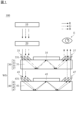
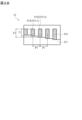
図1は、本開示のいくつかの実施形態による表示装置100を示す概略図である。いくつかの構成要素は、図1では実際の構造で示されておらず、表示装置100のいくつかの構成要素は、簡潔にするために省略されていることに留意されたい。また、表示装置100は、仮想現実(VR)、拡張現実(AR)、または混合現実(MR)に適用可能なニアアイディスプレイであることができるが、本発明はこれに限定されるものではない。
FIG. 1 is a schematic diagram illustrating a
図1に示すように、いくつかの実施形態では、表示装置100は画像ソース10を含む。例えば、画像ソース10は、仮想オブジェクトの画像を表示するように用いられることができる。画像ソース10は、可視波長範囲(例えば、約380nmから約750nmまでの波長)の異なる色の光を発することができる様々な光源であることができるが、本開示はこれらに限定されない。画像ソース10は、液晶ディスプレイ(LCD)、発光ダイオード(LED)、有機発光ダイオード(OLED)、アクティブマトリックス有機発光ダイオード(AMOLED)、シリコン上の液晶(LCoS)、デジタル光処理(DLP)、RGBレーザー、その他の適用可能なデバイス、またはそれらの組み合わせを含むことができる。
As shown in FIG. 1, in some embodiments, a
図1に示すように、いくつかの実施形態では、表示装置100は、画像ソース10からの光(例えば、赤色光R、緑色光G、および/または青色光B)を結合するように構成された導波路構造WSを含む。図1は、導波路構造WSの断面図を示していることに留意されたい。図1に示すように、いくつかの実施形態では、導波路構造WSは、互いに積層された導波路結合器30および導波路結合器40を含む。特に、導波路結合器30は、導波路結合器40上に配置される。
As shown in FIG. 1, in some embodiments,
図1に示されるように、いくつかの実施形態では、導波路結合器30は導波路板31を含む。例えば、導波路板31は、約1.5~約3.0の範囲で一定の屈折率を有する透明な誘電材料(例えば、ガラス)を含むことができるが、本開示はこれに限定されない。さらに、導波路板31は、化学気相堆積(CVD)プロセス、原子層堆積(ALD)プロセス、スピンコーティングプロセス、その他の適用可能なプロセス、またはそれらの組み合わせなどの堆積プロセスによって形成されることができるが、本開示は、これらに限定されない。
As shown in FIG. 1, in some embodiments,
図1に示すように、いくつかの実施形態では、導波路結合器30は、導波路板31上に配置された入力カプラ33を含む。図1に示すように、いくつかの実施形態では、導波路結合器30の入力カプラ33はグレーティングピラー331を含み、各グレーティングピラー331は徐々に変化する屈折率を有する。いくつかの実施形態では、徐々に変化する屈折率は、約1.4~約3.5の範囲にある。入力カプラ33に含まれる複数のグレーティングピラー331は、コリメータ20から出力される平行光の一部を導波路板31の内側に向けて屈折させるように構成されてもよい。
As shown in FIG. 1, in some embodiments,
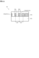
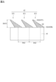
図2は、本開示のいくつかの実施形態による導波路板31およびグレーティングピラー331を示す部分断面図である。いくつかの実施形態では、各グレーティングピラー331は積層S1(図2を参照)を有し、2~30の積層S1が存在する。例えば、図2に示されるように、各グレーティングピラー331は積層S1を有し、11の積層S1が存在するが、本開示はこれらに限定されない。また、積層S1は、堆積プロセスによって形成されることができる。堆積プロセスの例は上述されており、ここでは繰り返されない。
FIG. 2 is a partial cross-sectional view illustrating a
いくつかの実施形態では、グレーティングピラー331の積層S1は、異なる材料を含むかまたは異なる濃度を有し、グレーティングピラー331は徐々に変化する屈折率を有するようにする。いくつかの実施形態では、グレーティングピラー331の徐々に変化する屈折率は、最大屈折率(例えば、グレーティングピラー331の底部にあるスタック層S1Bの屈折率)および最小屈折率(例えば、グレーティングピラー331の頂部にあるスタック層S1Tの屈折率)を有し、最大屈折率と最小屈折率との差は0より大きく、約2.1以下である。言い換えると、複数のグレーティングピラー331は、最大屈折率から最小屈折率の差が0より大きく、約2.1以下であり、屈折率が最大屈折率から最小屈折率まで徐々に変化するように、構成されてもよい。
In some embodiments, the stack S1 of grating
例えば、グレーティングピラー331の上部にある積層S1Tの屈折率は、約1.77であることができ、グレーティングピラー331の底部にある積層S1Bの屈折率は、約2.40であることができ、積層S1Bの屈折率と積層S1Tの屈折率との差は約0.63であるが、本開示はこれに限定されない。
For example, the refractive index of the stack S1T at the top of the
また、積層S1Tと積層S1Bとの間の積層の屈折率は、約1.77~約2.40の範囲にある。即ち、グレーティングピラー331は上部から底部に徐々に増加する屈折率を有することができるが、本開示はこれに限定されない。
Also, the refractive index of the stack between stack S1T and stack S1B is in the range of about 1.77 to about 2.40. That is, the
図2に示された実施形態では、各積層S1は同一の厚さを有するが、本発明はこれに限定されない。いくつかの他の実施形態では、積層S1の厚さは異なる。図2に示されるように、いくつかの実施形態では、積層S1の全高H331は、約40nm~約1000nmの範囲にある。 In the embodiment shown in FIG. 2, each stack S1 has the same thickness, but the invention is not limited thereto. In some other embodiments, the thickness of the stack S1 is different. As shown in FIG. 2, in some embodiments, the total height H331 of the stack S1 ranges from about 40 nm to about 1000 nm.
図1および図2に示されるように、いくつかの実施形態では、グレーティングピラー331は周期的な配列で形成され、この周期的な配列の周期P33は、約326nmなど、約250nm~約750nmの範囲にある。換言すれば、2つの隣接するグレーティングピラー331間の距離は一定であり得るが、本開示はこれに限定されない。レーティングピラー331は、導波路板31の上面に沿う方向で、周期的に配列されてもよい。
As shown in FIGS. 1 and 2, in some embodiments, grating
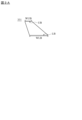
図3Aは、本開示のいくつかの実施形態によるグレーティングピラー331を示す拡大図である。図1および図3Aに示されるように、導波路構造WSの断面図から見て、各グレーティングピラー331のプロファイル(断面形状)は台形である。なお、導波路構造WSの断面は、導波路板31の上面に対して垂直な面である。図3Aに示されるように、いくつかの実施形態では、各グレーティングピラー331のプロファイルは、2つの平行な辺、上底UBおよび下底LBを有し、下底LBは上底UBより導波路板31に近い。
FIG. 3A is an enlarged view of a
図3Aに示されるように、いくつかの実施形態では、下底LBは上底UBより長い。即ち、下底LBの幅WLBは、上底UBの幅WUBより大きくてもよいが、これに限定されない。図1および図3Aに示されるように、グレーティングピラー331の下底LBは、導波路板31に取り付けられることができるが、本発明はこれに限定されない。
As shown in FIG. 3A, in some embodiments, the lower base LB is longer than the upper base UB. That is, the width WLB of the lower base LB may be larger than the width WUB of the upper base UB, but is not limited thereto. As shown in FIGS. 1 and 3A, the lower base LB of the
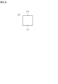
図3B~図3Eは、本開示のいくつかの他の実施形態によるグレーティングピラー331を示す異なる拡大図である。いくつかの実施形態では、導波路構造WSの断面図から見て、各グレーティングピラー331のプロファイルは、2つの平行な辺を有する。
3B-3E are different enlarged views showing
図3Bに示されるように、各グレーティングピラー331のプロファイルは長方形であり、2つの平行な辺は上辺USと下辺LSである。図3Cに示されるように、各グレーティングピラー331のプロファイルは平行四辺形であり、2つの平行な辺は上辺USおよび下辺LSである。図3Dに示されるように、各グレーティングピラー331のプロファイルは等脚台形であり、2つの平行な辺は上底UBと下底LBである。図3Eに示されるように、各グレーティングピラー331のプロファイルは正方形であり、2つの平行な辺は上辺USおよび下辺LSである。各グレーティングピラー331のプロファイルは、図3A~図3Eに限定されず、必要に応じて変更されることができる。
As shown in FIG. 3B, the profile of each
図1に示されるように、いくつかの実施形態では、導波路結合器30は、導波路板31上に配置され、入力カプラ33に隣接するエキスパンダー35をさらに含む。例えば、エキスパンダー35は、二次元(2D)瞳拡大技術(pupil expansion technique)を用いることができ、表示画像を解放するグレーティング構造を含むことができるが、本開示はこれに限定されない。
As shown in FIG. 1, in some embodiments,
図4Aは、本開示のいくつかの実施形態によるエキスパンダー35を示す部分断面図である。図4Aに示すように、いくつかの実施形態では、エキスパンダー35はグレーティングピラー353を含み、2つの隣接するグレーティングピラー353間の距離は一定である。換言すれば、いくつかの実施形態では、グレーティングピラー353は周期的な配列で形成され、この周期的な配列の周期P1は一定である。グレーティングピラー353は、図4Aの導波路板351上に配置されるが、導波路板351は、必要に応じて調整され得る別の導波路板または導波路板31の一部であってもよいことに留意されたい。
FIG. 4A is a partial cross-sectional view of an
いくつかの実施形態では、グレーティングピラー353は異なる幅を有する。例えば、図4Aに示されるように、グレーティングピラー353-1の幅W1は、隣接するグレーティングピラー353-2の幅W2より短いが、本開示はこれに限定されない。
In some embodiments, grating
図4Bは、本開示のいくつかの他の実施形態によるエキスパンダー35を示す部分断面図である。同様に、図4Bに示すように、エキスパンダー35はグレーティングピラー353を含み、2つの隣接するグレーティングピラー353間の距離は一定である。換言すれば、いくつかの実施形態では、グレーティングピラー353は周期的な配列で形成され、この周期的な配列の周期P1は一定である。
FIG. 4B is a partial cross-sectional view of an
いくつかの実施形態では、グレーティングピラー353は異なる厚さを有する。例えば、図4Bに示されるように、グレーティングピラー353-1の厚さT1は、隣接するグレーティングピラー353-2の厚さT2より小さいが、本開示はこれに限定されない。なお、図4Bに示すように、各グレーティングピラー353の上面は同じ高さに位置しており、各グレーティングピラー353の下面(底面)は異なる高さに位置してもよい。
In some embodiments, grating
図1に示されるように、いくつかの実施形態では、導波路結合器30は、導波路板31上に配置された出力カプラ37を含む。より詳細には、エキスパンダー35は、導波路板31の上面において、入力カプラ33と出力カプラ37との間に配置される。
As shown in FIG. 1, in some embodiments,
図1に示すように、導波路結合器40は、導波路結合器30と同様の構造を有する。図1に示されるように、いくつかの実施形態では、導波路結合器40は、導波路板41、および導波路板41上に配置された入力カプラ43を含む。図1に示されるように、いくつかの実施形態では、導波路結合器40の入力カプラ43は、グレーティングピラー431を含む。
As shown in FIG. 1,
図5は、本開示のいくつかの実施形態による導波路板41およびグレーティングピラー431を示す部分断面図である。いくつかの実施形態では、各グレーティングピラー431は積層S2(図5を参照)を有し、2~30の積層S2が存在する。例えば、図5に示されるように、各グレーティングピラー431は積層S2を有し、11の積層S2が存在するが、本開示はこれらに限定されない。いくつかの他の実施形態では、グレーティングピラー431の積層S2の数は、グレーティングピラー331の積層S1の数と異なる。また、積層S2は、堆積プロセスによって形成されることができる。堆積プロセスの例は上述されており、ここでは繰り返されない。
FIG. 5 is a partial cross-sectional view illustrating
いくつかの実施形態では、グレーティングピラー431の積層S2は、同じ材料を含むかまたは同じ濃度を有し、グレーティングピラー431は一定の屈折率を有するようにする。例えば、グレーティングピラー431の上部にある積層S2Tの屈折率は、約2.40であることができ、グレーティングピラー431の底部にある積層S2Bの屈折率は、約2.40であることができ、積層S2Bの屈折率と積層S2Tの屈折率との差は約0であるが、本発明はこれに限定されない。
In some embodiments, the stacks S2 of grating
いくつかの他の実施形態では、グレーティングピラー431の積層S2は、グレーティングピラー331の積層S1と同様である。即ち、グレーティングピラー431の積層S2は、異なる材料を含むか、または異なる濃度を有し、グレーティングピラー431は徐々に変化する屈折率を有するようにする。
In some other embodiments, stack S2 of
図5に示された実施形態では、各積層S2は同じ厚さを有するが、本発明はこれに限定されない。いくつかの他の実施形態では、積層S2の厚さは異なる。図5に示されるように、いくつかの実施形態では、積層S2の全高H431は、約40nm~約1000nmの範囲にある。 In the embodiment shown in FIG. 5, each stack S2 has the same thickness, but the invention is not limited thereto. In some other embodiments, the thickness of the stack S2 is different. As shown in FIG. 5, in some embodiments, the total height H431 of stack S2 ranges from about 40 nm to about 1000 nm.
図1および図5に示されるように、いくつかの実施形態では、グレーティングピラー431は周期的な配列で形成され、周期的な配列の周期P43は、約449nmなど、約250nm~約750nmの範囲にある。換言すれば、2つの隣接するグレーティングピラー431間の距離は一定であり得るが、本開示はこれに限定されない。いくつかの他の実施形態では、グレーティングピラー431のプロファイルは、各グレーティングピラー331のプロファイルと異なり、必要に応じて調整されることができる。
As shown in FIGS. 1 and 5, in some embodiments, grating
図1に示されるように、いくつかの実施形態では、導波路結合器40は、導波路板41上に配置され、入力カプラ43に隣接するエキスパンダー45をさらに含む。同様に、エキスパンダー45は、二次元(2D)瞳拡大技術を用いることができ、表示画像を解放するグレーティング構造を含むことができるが、本開示はこれに限定されない。この実施形態では、エキスパンダー45は、エキスパンダー35と同様の構造を有するが、本開示はこれに限定されない。
As shown in FIG. 1, in some embodiments,
図1に示されるように、いくつかの実施形態では、導波路結合器40は、導波路板41上に配置された出力カプラ47を含む。より詳細には、エキスパンダー45は、入力カプラ43と出力カプラ47との間に配置される。
As shown in FIG. 1, in some embodiments,
いくつかの実施形態では、導波路結合器30および導波路結合器40は、異なる色の光を結合するように用いられ、異なる色の光は、約380nm~約750nmの波長を有する(例えば、可視光)。すなわち、導波路結合器30および導波路結合器40は、それぞれの導波路結合器30,40で異なる色の光を結合するように用いられている。例えば、図1に示されるように、導波路結合器30は緑色光Gと青色光Bを結合するように用いられることができ、導波路結合器40は赤色光Rと緑色光Gを結合するように用いられることができるが、本開示はこれらに限定されない。
In some embodiments,
図1に示されるように、いくつかの実施形態では、表示装置100は、画像ソース10と導波路構造WSとの間に配置されたコリメータ20をさらに含む。コリメータ20は、画像ソース10からの発散光または他の放射線を平行ビームに変換し、画像ソース10からの光が導波路構造WSに円滑に入ることができるようにする。図1に示されるように、画像ソース10からの画像(光)は、コリメータ20を介して導波路構造WSに入り、次いでユーザーの目Eに伝達されて提示され得る。
As shown in FIG. 1, in some embodiments,
従来のニアアイディスプレイに比べ、本開示の実施形態による表示装置100は、導波路構造WSにより、結合効率を、例えば約62%から約83%に効果的に向上させることができる。さらに、ユーザーの視野(FoV)も、例えば約42.5°から約60°に改善され、これは固有の材料の制限に近い値である。
Compared to a conventional near-eye display, the
図6は、本開示のいくつかの他の実施形態による表示装置102を示す概略図である。同様に、いくつかの構成要素は、図6においてそれらの実際の構造で示されておらず、表示装置102のいくつかの構成要素は、簡潔にするために省略されている。
FIG. 6 is a schematic diagram illustrating a
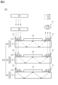
図6に示すように、表示装置102は、表示装置100と同様の構造を有する。いくつかの実施形態では、表示装置102の導波路構造WSは、導波路結合器30および導波路結合器40上に積層された導波路結合器50をさらに含む。より詳細には、導波路結合器40は、導波路結合器30と導波路結合器50との間に配置されることができるが、本開示は、これに限定されない。
As shown in FIG. 6, the
図6に示すように、導波路結合器50は、導波路結合器30または導波路結合器40と同様の構造を有する。図6に示されるように、いくつかの実施形態では、導波路結合器50は、導波路板51、および導波路板51上に配置された入力カプラ53を含む。図6に示されるように、いくつかの実施形態では、導波路結合器50の入力カプラ53は、グレーティングピラー531を含む。
As shown in FIG. 6,
図6に示されるように、いくつかの実施形態では、導波路結合器50は、導波路板51上に配置され、入力カプラ53に隣接するエキスパンダー55をさらに含む。同様に、エキスパンダー55は、二次元(2D)瞳拡大技術を用いることができ、表示画像を解放するグレーティング構造を含むことができるが、本開示はこれに限定されない。この実施形態では、エキスパンダー55は、エキスパンダー35またはエキスパンダー45と同様の構造を有するが、本開示はこれに限定されない。
As shown in FIG. 6, in some embodiments,
図6に示されるように、いくつかの実施形態では、導波路結合器50は、導波路板51上に配置された出力カプラ57を含む。より詳細には、エキスパンダー55は、入力カプラ53と出力カプラ57との間に配置される。
As shown in FIG. 6, in some embodiments,
いくつかの実施形態では、導波路結合器30、導波路結合器40、および導波路結合器50は、異なる色の光を結合するように用いられ、異なる色の光は、約380nm~約750nmの波長を有する(例えば、可視光)。例えば、図6に示されるように、導波路結合器30は青色光Bと結合するように用いられることができ、導波路結合器40は緑色光Gと結合するように用いられることができ、導波路結合器50は赤色光Rと結合するように用いられることができるが、本開示はこれらに限定されない。
In some embodiments,
導波路管結合器の数は、図1に示される実施形態(2つの導波路結合器がある)または図6に示される実施形態(3つの導波路結合器がある)に限定されないことに注意されたい。いくつかの実施形態では、2つ以上の導波路結合器がある。 Note that the number of waveguide couplers is not limited to the embodiment shown in FIG. 1 (there are two waveguide couplers) or the embodiment shown in FIG. 6 (there are three waveguide couplers). I want to be In some embodiments, there are two or more waveguide couplers.
要約すると、本開示のいくつかの実施形態では、表示装置(例えば、AR、VE、またはMR装置)は、互いに積層された導波路結合器を含む導波路構造を含む。導波路結合器の少なくとも1つの入力カプラは、徐々に変化する屈折率を有し、結合効率とユーザーの視野(FoV)を効果的に改善することができる。 In summary, in some embodiments of the present disclosure, a display device (eg, an AR, VE, or MR device) includes a waveguide structure that includes waveguide couplers stacked together. At least one input coupler of the waveguide coupler has a gradually changing refractive index, which can effectively improve the coupling efficiency and user's field of view (FoV).
前述の内容は、当業者が本開示の態様をよりよく理解できるように、いくつかの実施形態の特徴を概説している。当業者は、同じ目的を実行するため、および/または本明細書に導入される実施形態の同じ利点を達成するための他のプロセスおよび構造を設計または修正するための基礎として本開示を容易に使用できることを理解できる。当業者はまた、そのような同等の構造が本開示の精神および範囲から逸脱せず、且つそれらは、本開示の趣旨および範囲から逸脱することなく、本明細書で様々な変更、置換、および代替を行うことができることを理解するべきである。従って、保護の範囲は特許請求の範囲を通じて決定される必要がある。さらに、本開示のいくつかの実施形態が上記に開示されているが、それらは、本開示の範囲を限定することを意図していない。 The foregoing has outlined features of some embodiments so that those skilled in the art can better understand aspects of the disclosure. Those skilled in the art will readily utilize this disclosure as a basis for designing or modifying other processes and structures to carry out the same purposes and/or achieve the same advantages of the embodiments introduced herein. Understand that it can be used. Those skilled in the art will also appreciate that such equivalent constructions do not depart from the spirit and scope of this disclosure, and that they may make various changes, substitutions, and modifications herein without departing from the spirit and scope of this disclosure. It should be understood that substitutions can be made. Therefore, the scope of protection needs to be determined through the claims. Furthermore, although some embodiments of the present disclosure have been disclosed above, they are not intended to limit the scope of the present disclosure.
本明細書全体にわたる特徴、利点、または同様の用語への言及は、本開示で実現され得る全ての特徴および利点が、本開示の任意の単一の実施形態で実現されるべきまたは実現され得ることを意味するのではない。むしろ、特徴および利点に言及する用語は、実施形態に関連して説明される特定の特徴、利点、または特性が本開示の少なくとも1つの実施形態に含まれることを意味すると理解される。従って、本明細書全体にわたる特徴および利点、ならびに類似の用語の議論は、必ずしもそうではないが、同じ実施形態を指すことがある。 References throughout this specification to features, advantages, or similar terms indicate that all features and advantages that can be realized in this disclosure are or can be realized in any single embodiment of this disclosure. It doesn't mean that. Rather, terms referring to features and advantages are understood to mean that a particular feature, advantage, or property described in connection with an embodiment is included in at least one embodiment of the present disclosure. Accordingly, discussions of features and advantages and similar terminology throughout this specification may, but do not necessarily, refer to the same embodiment.
さらに、1つまたは複数の実施形態では、本開示の説明された特徴、利点、および特性は、任意の適切な方法で組み合わせてもよい。当業者は、本明細書の説明に基づいて、特定の実施形態の1つまたは複数の特定の特徴または利点なしに本開示を実施できることを認識するであろう。他の例では、本開示の全ての実施形態に存在しない可能性がある、追加の特徴および利点が特定の実施形態において認識され得る。 Furthermore, the described features, advantages, and characteristics of this disclosure may be combined in any suitable manner in one or more embodiments. Those skilled in the art will recognize, based on the description herein, that the present disclosure may be practiced without one or more of the particular features or advantages of the particular embodiments. In other examples, additional features and advantages may be realized in particular embodiments that may not be present in all embodiments of this disclosure.
100、102 表示装置
10 画像ソース
20 コリメータ
30、40、50 導波路結合器
31、351、41、51 導波路板
33、43、53 入力カプラ
331、353、353-1、353-2、431、531 グレーティングピラー
35、45、55 エキスパンダー
37、47、57 出力カプラ
B 青色光
E 目
G 緑色光
H331、H431 全高
LB 下底
LS 下辺
P1、P33、P43 周期
R 赤色光
S1、S1B、S1T、S2、S2B、S2T 積層
T1、T2 厚さ
UB 上底
US 上辺
W1、W2 幅
WS 導波路構造
WLB 下底LBの幅
WUB 上底UBの幅
100, 102
Claims (10)
各前記導波路結合器は、
導波路板、および
前記導波路板上に配置された入力カプラを含み、
少なくとも1つの前記導波路結合器の前記入力カプラは第1のグレーティングピラーを含み、
各前記第1のグレーティングピラーは徐々に変化する屈折率を有する導波路構造。 including waveguide couplers stacked on top of each other;
Each said waveguide coupler is
a waveguide plate; and an input coupler disposed on the waveguide plate;
the input coupler of at least one of the waveguide couplers includes a first grating pillar;
Each first grating pillar has a waveguide structure with a gradually changing refractive index.
前記導波路結合器は、異なる色の光を結合するように用いられ、
前記異なる色の光は、380nm~750nmの波長を有する請求項1に記載の導波路構造。 the number of waveguide couplers is two or more waveguide couplers,
the waveguide coupler is used to couple light of different colors;
The waveguide structure according to claim 1, wherein the different colored lights have wavelengths of 380 nm to 750 nm.
前記積層の数は2以上、30以下であり、
前記積層の全高は、40nm~1000nmの範囲にある請求項1に記載の導波路構造。 each said first grating pillar has a lamination;
The number of laminated layers is 2 or more and 30 or less,
The waveguide structure according to claim 1, wherein the total height of the stack is in the range of 40 nm to 1000 nm.
前記最大屈折率と前記最小屈折率との差は0より大きく、2.1以下であり、
前記徐々に変化する屈折率は、1.4~3.5の範囲にあり、
前記導波路板は、1.5~3.0の範囲で一定の屈折率を有する請求項1に記載の導波路構造。 the gradually changing refractive index has a maximum refractive index and a minimum refractive index;
The difference between the maximum refractive index and the minimum refractive index is greater than 0 and 2.1 or less,
the gradually changing refractive index is in the range of 1.4 to 3.5;
The waveguide structure according to claim 1, wherein the waveguide plate has a constant refractive index in the range of 1.5 to 3.0.
前記周期的な配列の周期は、250nm~750nmの範囲にある請求項1に記載の導波路構造。 the first grating pillars are formed in a periodic array;
The waveguide structure according to claim 1, wherein the period of the periodic array is in the range of 250 nm to 750 nm.
前記導波路板上に配置され、前記入力カプラに隣接するエキスパンダーをさらに含み、
前記エキスパンダーは第2のグレーティングピラーを含み、
2つの隣接する第2のグレーティングピラー間の距離は一定である請求項1に記載の導波路構造。 Each said waveguide coupler is
further comprising an expander disposed on the waveguide plate and adjacent the input coupler;
the expander includes a second grating pillar;
The waveguide structure according to claim 1, wherein the distance between two adjacent second grating pillars is constant.
前記エキスパンダーは、前記入力カプラと前記出力カプラとの間に配置される請求項7に記載の導波路構造。 each said waveguide coupler further includes an output coupler disposed on said waveguide plate;
8. The waveguide structure of claim 7, wherein the expander is located between the input coupler and the output coupler.
前記画像ソースからの光を結合するように構成された導波路構造を含み、
前記導波路構造は、互いに積層された導波路結合器を含み、
各前記導波路結合器は、導波路板、および前記導波路板上に配置された入力カプラを含み、
少なくとも1つの前記導波路結合器の前記入力カプラは、第1のグレーティングピラーを含み、各前記第1のグレーティングピラーは徐々に変化する屈折率を有する表示装置。 an image source and a waveguide structure configured to couple light from the image source;
The waveguide structure includes waveguide couplers stacked on top of each other,
Each of the waveguide couplers includes a waveguide plate and an input coupler disposed on the waveguide plate;
The input coupler of at least one of the waveguide couplers includes a first grating pillar, each first grating pillar having a gradually varying index of refraction.
Applications Claiming Priority (2)
| Application Number | Priority Date | Filing Date | Title |
|---|---|---|---|
| US17/739,888 | 2022-05-09 | ||
| US17/739,888 US20230359031A1 (en) | 2022-05-09 | 2022-05-09 | Waveguide structure and display device using the same |
Publications (2)
| Publication Number | Publication Date |
|---|---|
| JP2023166322A true JP2023166322A (en) | 2023-11-21 |
| JP7546638B2 JP7546638B2 (en) | 2024-09-06 |
Family
ID=82839242
Family Applications (1)
| Application Number | Title | Priority Date | Filing Date |
|---|---|---|---|
| JP2022169058A Active JP7546638B2 (en) | 2022-05-09 | 2022-10-21 | Waveguide structure and display device using same |
Country Status (6)
| Country | Link |
|---|---|
| US (1) | US20230359031A1 (en) |
| EP (1) | EP4276514B1 (en) |
| JP (1) | JP7546638B2 (en) |
| KR (1) | KR102809547B1 (en) |
| CN (1) | CN117031616A (en) |
| TW (1) | TW202414006A (en) |
Cited By (1)
| Publication number | Priority date | Publication date | Assignee | Title |
|---|---|---|---|---|
| JP2024050384A (en) * | 2022-09-29 | 2024-04-10 | 采▲ぎょく▼科技股▲ふん▼有限公司 | Method for forming a grating device |
Citations (13)
| Publication number | Priority date | Publication date | Assignee | Title |
|---|---|---|---|---|
| JP2008139618A (en) * | 2006-12-04 | 2008-06-19 | Ricoh Co Ltd | Optical element and optical device |
| JP2009186794A (en) * | 2008-02-07 | 2009-08-20 | Sony Corp | Optical device and image display device |
| JP2010262320A (en) * | 2003-03-13 | 2010-11-18 | Asahi Glass Co Ltd | Diffraction element and optical device |
| JP2015118273A (en) * | 2013-12-18 | 2015-06-25 | マイクロソフト コーポレーション | NED polarization system for wavelength passage |
| JP2017004004A (en) * | 2012-03-26 | 2017-01-05 | 旭硝子株式会社 | Transmission type diffraction element |
| US20190227316A1 (en) * | 2018-01-23 | 2019-07-25 | Facebook, Inc. | Slanted surface relief grating for rainbow reduction in waveguide display |
| US20200081246A1 (en) * | 2017-05-08 | 2020-03-12 | Dispelix Oy | Diffractive display, lightguide element and projector therefor, and method for displaying image |
| US20200225498A1 (en) * | 2019-01-11 | 2020-07-16 | North Inc. | Single RGB Combiner with Large Field of View |
| US20200278498A1 (en) * | 2016-01-06 | 2020-09-03 | Vuzix Corporation | Two channel imaging light guide with dichroic reflector |
| US20210141146A1 (en) * | 2019-11-08 | 2021-05-13 | Magic Leap, Inc. | Metasurfaces with light-redirecting structures including multiple materials and methods for fabricating |
| WO2021133965A1 (en) * | 2019-12-26 | 2021-07-01 | Facebook Technologies, Llc | Gradient refractive index grating for display leakage reduction |
| WO2021169383A1 (en) * | 2020-02-28 | 2021-09-02 | 苏州苏大维格科技集团股份有限公司 | Apparatus for displaying augmented reality image, and system comprising apparatus |
| CN217156853U (en) * | 2021-12-22 | 2022-08-09 | 深圳光峰科技股份有限公司 | Display device and diffractive optical element |
Family Cites Families (10)
| Publication number | Priority date | Publication date | Assignee | Title |
|---|---|---|---|---|
| JP3916200B2 (en) | 2000-03-24 | 2007-05-16 | フジノン株式会社 | Diffraction lens and optical pickup device using the same |
| JP4209154B2 (en) | 2002-08-15 | 2009-01-14 | アルプス電気株式会社 | Diffractive optical element |
| WO2018039273A1 (en) * | 2016-08-22 | 2018-03-01 | Magic Leap, Inc. | Dithering methods and apparatus for wearable display device |
| FI129400B (en) * | 2017-12-22 | 2022-01-31 | Dispelix Oy | Diffractive waveguide element and diffractive waveguide display |
| FI129359B (en) * | 2018-03-28 | 2021-12-31 | Dispelix Oy | Diffractive grating |
| US11137603B2 (en) * | 2019-06-20 | 2021-10-05 | Facebook Technologies, Llc | Surface-relief grating with patterned refractive index modulation |
| US11391950B2 (en) * | 2019-06-26 | 2022-07-19 | Meta Platforms Technologies, Llc | Techniques for controlling effective refractive index of gratings |
| US10845526B1 (en) * | 2019-08-23 | 2020-11-24 | Facebook Technologies, Llc | Outward coupling suppression in waveguide display |
| JP7420926B2 (en) * | 2019-09-11 | 2024-01-23 | マジック リープ, インコーポレイテッド | Display device with a diffraction grating with reduced polarization sensitivity |
| KR20230060506A (en) * | 2020-09-01 | 2023-05-04 | 스냅 인코포레이티드 | Diffraction grating design method for augmented reality or virtual reality display and diffraction grating for augmented reality or virtual reality display |
-
2022
- 2022-05-09 US US17/739,888 patent/US20230359031A1/en active Pending
- 2022-08-04 EP EP22188813.4A patent/EP4276514B1/en active Active
- 2022-08-08 KR KR1020220098522A patent/KR102809547B1/en active Active
- 2022-10-21 JP JP2022169058A patent/JP7546638B2/en active Active
-
2023
- 2023-03-08 TW TW112108534A patent/TW202414006A/en unknown
- 2023-04-14 CN CN202310398135.7A patent/CN117031616A/en active Pending
Patent Citations (13)
| Publication number | Priority date | Publication date | Assignee | Title |
|---|---|---|---|---|
| JP2010262320A (en) * | 2003-03-13 | 2010-11-18 | Asahi Glass Co Ltd | Diffraction element and optical device |
| JP2008139618A (en) * | 2006-12-04 | 2008-06-19 | Ricoh Co Ltd | Optical element and optical device |
| JP2009186794A (en) * | 2008-02-07 | 2009-08-20 | Sony Corp | Optical device and image display device |
| JP2017004004A (en) * | 2012-03-26 | 2017-01-05 | 旭硝子株式会社 | Transmission type diffraction element |
| JP2015118273A (en) * | 2013-12-18 | 2015-06-25 | マイクロソフト コーポレーション | NED polarization system for wavelength passage |
| US20200278498A1 (en) * | 2016-01-06 | 2020-09-03 | Vuzix Corporation | Two channel imaging light guide with dichroic reflector |
| US20200081246A1 (en) * | 2017-05-08 | 2020-03-12 | Dispelix Oy | Diffractive display, lightguide element and projector therefor, and method for displaying image |
| US20190227316A1 (en) * | 2018-01-23 | 2019-07-25 | Facebook, Inc. | Slanted surface relief grating for rainbow reduction in waveguide display |
| US20200225498A1 (en) * | 2019-01-11 | 2020-07-16 | North Inc. | Single RGB Combiner with Large Field of View |
| US20210141146A1 (en) * | 2019-11-08 | 2021-05-13 | Magic Leap, Inc. | Metasurfaces with light-redirecting structures including multiple materials and methods for fabricating |
| WO2021133965A1 (en) * | 2019-12-26 | 2021-07-01 | Facebook Technologies, Llc | Gradient refractive index grating for display leakage reduction |
| WO2021169383A1 (en) * | 2020-02-28 | 2021-09-02 | 苏州苏大维格科技集团股份有限公司 | Apparatus for displaying augmented reality image, and system comprising apparatus |
| CN217156853U (en) * | 2021-12-22 | 2022-08-09 | 深圳光峰科技股份有限公司 | Display device and diffractive optical element |
Cited By (3)
| Publication number | Priority date | Publication date | Assignee | Title |
|---|---|---|---|---|
| JP2024050384A (en) * | 2022-09-29 | 2024-04-10 | 采▲ぎょく▼科技股▲ふん▼有限公司 | Method for forming a grating device |
| JP7550259B2 (en) | 2022-09-29 | 2024-09-12 | 采▲ぎょく▼科技股▲ふん▼有限公司 | Method for forming a grating device |
| US12487384B2 (en) | 2022-09-29 | 2025-12-02 | Visera Technologies Company Limited | Method forming grating device |
Also Published As
| Publication number | Publication date |
|---|---|
| US20230359031A1 (en) | 2023-11-09 |
| CN117031616A (en) | 2023-11-10 |
| EP4276514B1 (en) | 2025-07-02 |
| KR102809547B1 (en) | 2025-05-19 |
| JP7546638B2 (en) | 2024-09-06 |
| KR20230157211A (en) | 2023-11-16 |
| EP4276514A1 (en) | 2023-11-15 |
| TW202414006A (en) | 2024-04-01 |
Similar Documents
| Publication | Publication Date | Title |
|---|---|---|
| AU2015298504B2 (en) | Exit pupil expanding diffractive optical waveguiding device | |
| JP6960994B2 (en) | Externally coupled diffraction grating for augmented reality systems | |
| CN110140008B (en) | Multi-view backlighting using fluorescent multibeam elements | |
| JP6633087B2 (en) | Three-dimensional (3D) electronic display | |
| US8508848B2 (en) | Exit pupil expanders with wide field-of-view | |
| CN111194422A (en) | Waveguides for Augmented Reality or Virtual Reality Displays | |
| US12164119B2 (en) | Multiview display and method | |
| CN114710965A (en) | High field of view optical device for coupling incident light | |
| CN113544551A (en) | Optical device | |
| CN111864119B (en) | Display devices and near-eye display devices | |
| CN106324847A (en) | Three-dimensional display device | |
| JP7046987B2 (en) | How to use multi-view backlight, multi-view display and offset multi-beam elements | |
| US20170176669A1 (en) | Directional backlight, 3d image display apparatus having the same, and method of manufacturing the same | |
| EP4127789B1 (en) | Unpolarized light grating in-coupler | |
| CN114911058B (en) | Method for realizing single-chip full-color by using diffractive optical waveguide, diffractive optical waveguide and device | |
| JP7546638B2 (en) | Waveguide structure and display device using same | |
| CN115398315A (en) | Waveguide display system with wide field of view | |
| CN113795780A (en) | Multi-view display with shifted color sub-pixels and method | |
| CN111837070A (en) | Horizontal parallax multi-view display and method with tilted multi-beam columns | |
| CN114578480A (en) | A two-dimensional grating, optical waveguide and near-eye display system | |
| EP4176302A1 (en) | Full-color waveguide combiner with embedded metagrating | |
| CN115398284B (en) | Non-polarized light grating in-coupler | |
| CN119126406A (en) | Display panel, preparation method and application thereof, AR near-eye display device | |
| HK40068557A (en) | Multiview display and method having shifted color sub-pixels | |
| WO2013157210A1 (en) | Diffusion element, optical element, light-emitting device, and projection device |
Legal Events
| Date | Code | Title | Description |
|---|---|---|---|
| A621 | Written request for application examination |
Free format text: JAPANESE INTERMEDIATE CODE: A621 Effective date: 20221021 |
|
| A131 | Notification of reasons for refusal |
Free format text: JAPANESE INTERMEDIATE CODE: A131 Effective date: 20230919 |
|
| A521 | Request for written amendment filed |
Free format text: JAPANESE INTERMEDIATE CODE: A523 Effective date: 20231215 |
|
| A131 | Notification of reasons for refusal |
Free format text: JAPANESE INTERMEDIATE CODE: A131 Effective date: 20240220 |
|
| A521 | Request for written amendment filed |
Free format text: JAPANESE INTERMEDIATE CODE: A523 Effective date: 20240509 |
|
| TRDD | Decision of grant or rejection written | ||
| A01 | Written decision to grant a patent or to grant a registration (utility model) |
Free format text: JAPANESE INTERMEDIATE CODE: A01 Effective date: 20240806 |
|
| A61 | First payment of annual fees (during grant procedure) |
Free format text: JAPANESE INTERMEDIATE CODE: A61 Effective date: 20240827 |
|
| R150 | Certificate of patent or registration of utility model |
Ref document number: 7546638 Country of ref document: JP Free format text: JAPANESE INTERMEDIATE CODE: R150 |