JP2021521629A - How to make a transistor - Google Patents
How to make a transistor Download PDFInfo
- Publication number
- JP2021521629A JP2021521629A JP2020554400A JP2020554400A JP2021521629A JP 2021521629 A JP2021521629 A JP 2021521629A JP 2020554400 A JP2020554400 A JP 2020554400A JP 2020554400 A JP2020554400 A JP 2020554400A JP 2021521629 A JP2021521629 A JP 2021521629A
- Authority
- JP
- Japan
- Prior art keywords
- layer
- semiconductor substrate
- etching
- region
- oxide
- Prior art date
- Legal status (The legal status is an assumption and is not a legal conclusion. Google has not performed a legal analysis and makes no representation as to the accuracy of the status listed.)
- Pending
Links
- 239000004065 semiconductor Substances 0.000 claims abstract description 65
- 239000000758 substrate Substances 0.000 claims abstract description 59
- 229920002120 photoresistant polymer Polymers 0.000 claims abstract description 40
- 230000004888 barrier function Effects 0.000 claims abstract description 32
- 238000005530 etching Methods 0.000 claims abstract description 23
- 239000002019 doping agent Substances 0.000 claims abstract description 20
- 239000007800 oxidant agent Substances 0.000 claims abstract description 13
- 239000011248 coating agent Substances 0.000 claims abstract description 12
- 238000000576 coating method Methods 0.000 claims abstract description 12
- 230000001590 oxidative effect Effects 0.000 claims abstract description 12
- 238000004519 manufacturing process Methods 0.000 claims abstract description 10
- 238000000034 method Methods 0.000 claims description 39
- 229910052581 Si3N4 Inorganic materials 0.000 claims description 22
- HQVNEWCFYHHQES-UHFFFAOYSA-N silicon nitride Chemical compound N12[Si]34N5[Si]62N3[Si]51N64 HQVNEWCFYHHQES-UHFFFAOYSA-N 0.000 claims description 22
- 230000005855 radiation Effects 0.000 claims description 11
- VYPSYNLAJGMNEJ-UHFFFAOYSA-N Silicium dioxide Chemical compound O=[Si]=O VYPSYNLAJGMNEJ-UHFFFAOYSA-N 0.000 claims description 8
- QVGXLLKOCUKJST-UHFFFAOYSA-N atomic oxygen Chemical compound [O] QVGXLLKOCUKJST-UHFFFAOYSA-N 0.000 claims description 6
- 239000001301 oxygen Substances 0.000 claims description 6
- 229910052760 oxygen Inorganic materials 0.000 claims description 6
- 238000001020 plasma etching Methods 0.000 claims description 5
- XKRFYHLGVUSROY-UHFFFAOYSA-N Argon Chemical compound [Ar] XKRFYHLGVUSROY-UHFFFAOYSA-N 0.000 claims description 4
- 235000012239 silicon dioxide Nutrition 0.000 claims description 4
- 239000000377 silicon dioxide Substances 0.000 claims description 4
- 238000002955 isolation Methods 0.000 claims description 3
- OKTJSMMVPCPJKN-UHFFFAOYSA-N Carbon Chemical compound [C] OKTJSMMVPCPJKN-UHFFFAOYSA-N 0.000 claims description 2
- PXGOKWXKJXAPGV-UHFFFAOYSA-N Fluorine Chemical compound FF PXGOKWXKJXAPGV-UHFFFAOYSA-N 0.000 claims description 2
- UFHFLCQGNIYNRP-UHFFFAOYSA-N Hydrogen Chemical compound [H][H] UFHFLCQGNIYNRP-UHFFFAOYSA-N 0.000 claims description 2
- 229910052786 argon Inorganic materials 0.000 claims description 2
- 229910052799 carbon Inorganic materials 0.000 claims description 2
- 239000012159 carrier gas Substances 0.000 claims description 2
- 229910052731 fluorine Inorganic materials 0.000 claims description 2
- 239000011737 fluorine Substances 0.000 claims description 2
- 239000008246 gaseous mixture Substances 0.000 claims description 2
- 239000001257 hydrogen Substances 0.000 claims description 2
- 229910052739 hydrogen Inorganic materials 0.000 claims description 2
- 239000006117 anti-reflective coating Substances 0.000 claims 2
- 239000004020 conductor Substances 0.000 claims 1
- 239000007789 gas Substances 0.000 claims 1
- 239000000126 substance Substances 0.000 claims 1
- 238000000151 deposition Methods 0.000 abstract description 6
- XUIMIQQOPSSXEZ-UHFFFAOYSA-N Silicon Chemical compound [Si] XUIMIQQOPSSXEZ-UHFFFAOYSA-N 0.000 description 7
- 229910052710 silicon Inorganic materials 0.000 description 7
- 239000010703 silicon Substances 0.000 description 7
- 108091006146 Channels Proteins 0.000 description 5
- 239000000463 material Substances 0.000 description 4
- 229910044991 metal oxide Inorganic materials 0.000 description 3
- 150000004706 metal oxides Chemical class 0.000 description 3
- 230000003647 oxidation Effects 0.000 description 3
- 238000007254 oxidation reaction Methods 0.000 description 3
- 239000000969 carrier Substances 0.000 description 2
- 238000005516 engineering process Methods 0.000 description 2
- 238000005286 illumination Methods 0.000 description 2
- 241000293849 Cordylanthus Species 0.000 description 1
- 102000004129 N-Type Calcium Channels Human genes 0.000 description 1
- 108090000699 N-Type Calcium Channels Proteins 0.000 description 1
- 230000001133 acceleration Effects 0.000 description 1
- ISQINHMJILFLAQ-UHFFFAOYSA-N argon hydrofluoride Chemical compound F.[Ar] ISQINHMJILFLAQ-UHFFFAOYSA-N 0.000 description 1
- 210000003323 beak Anatomy 0.000 description 1
- 230000015572 biosynthetic process Effects 0.000 description 1
- 230000000295 complement effect Effects 0.000 description 1
- 239000013078 crystal Substances 0.000 description 1
- 238000009792 diffusion process Methods 0.000 description 1
- 230000005669 field effect Effects 0.000 description 1
- 238000002347 injection Methods 0.000 description 1
- 239000007924 injection Substances 0.000 description 1
- 238000012986 modification Methods 0.000 description 1
- 230000004048 modification Effects 0.000 description 1
- 229910021420 polycrystalline silicon Inorganic materials 0.000 description 1
- 229920005591 polysilicon Polymers 0.000 description 1
- XLYOFNOQVPJJNP-UHFFFAOYSA-N water Chemical compound O XLYOFNOQVPJJNP-UHFFFAOYSA-N 0.000 description 1
Images


Classifications
-
- H—ELECTRICITY
- H01—ELECTRIC ELEMENTS
- H01L—SEMICONDUCTOR DEVICES NOT COVERED BY CLASS H10
- H01L21/00—Processes or apparatus adapted for the manufacture or treatment of semiconductor or solid state devices or of parts thereof
- H01L21/02—Manufacture or treatment of semiconductor devices or of parts thereof
- H01L21/04—Manufacture or treatment of semiconductor devices or of parts thereof the devices having at least one potential-jump barrier or surface barrier, e.g. PN junction, depletion layer or carrier concentration layer
- H01L21/18—Manufacture or treatment of semiconductor devices or of parts thereof the devices having at least one potential-jump barrier or surface barrier, e.g. PN junction, depletion layer or carrier concentration layer the devices having semiconductor bodies comprising elements of Group IV of the Periodic System or AIIIBV compounds with or without impurities, e.g. doping materials
- H01L21/26—Bombardment with radiation
- H01L21/263—Bombardment with radiation with high-energy radiation
- H01L21/265—Bombardment with radiation with high-energy radiation producing ion implantation
- H01L21/266—Bombardment with radiation with high-energy radiation producing ion implantation using masks
-
- H—ELECTRICITY
- H01—ELECTRIC ELEMENTS
- H01L—SEMICONDUCTOR DEVICES NOT COVERED BY CLASS H10
- H01L29/00—Semiconductor devices adapted for rectifying, amplifying, oscillating or switching, or capacitors or resistors with at least one potential-jump barrier or surface barrier, e.g. PN junction depletion layer or carrier concentration layer; Details of semiconductor bodies or of electrodes thereof ; Multistep manufacturing processes therefor
- H01L29/66—Types of semiconductor device ; Multistep manufacturing processes therefor
- H01L29/66007—Multistep manufacturing processes
- H01L29/66075—Multistep manufacturing processes of devices having semiconductor bodies comprising group 14 or group 13/15 materials
- H01L29/66227—Multistep manufacturing processes of devices having semiconductor bodies comprising group 14 or group 13/15 materials the devices being controllable only by the electric current supplied or the electric potential applied, to an electrode which does not carry the current to be rectified, amplified or switched, e.g. three-terminal devices
- H01L29/66409—Unipolar field-effect transistors
- H01L29/66477—Unipolar field-effect transistors with an insulated gate, i.e. MISFET
- H01L29/66568—Lateral single gate silicon transistors
- H01L29/66659—Lateral single gate silicon transistors with asymmetry in the channel direction, e.g. lateral high-voltage MISFETs with drain offset region, extended drain MISFETs
-
- H—ELECTRICITY
- H01—ELECTRIC ELEMENTS
- H01L—SEMICONDUCTOR DEVICES NOT COVERED BY CLASS H10
- H01L21/00—Processes or apparatus adapted for the manufacture or treatment of semiconductor or solid state devices or of parts thereof
- H01L21/70—Manufacture or treatment of devices consisting of a plurality of solid state components formed in or on a common substrate or of parts thereof; Manufacture of integrated circuit devices or of parts thereof
- H01L21/77—Manufacture or treatment of devices consisting of a plurality of solid state components or integrated circuits formed in, or on, a common substrate
- H01L21/78—Manufacture or treatment of devices consisting of a plurality of solid state components or integrated circuits formed in, or on, a common substrate with subsequent division of the substrate into plural individual devices
- H01L21/82—Manufacture or treatment of devices consisting of a plurality of solid state components or integrated circuits formed in, or on, a common substrate with subsequent division of the substrate into plural individual devices to produce devices, e.g. integrated circuits, each consisting of a plurality of components
- H01L21/822—Manufacture or treatment of devices consisting of a plurality of solid state components or integrated circuits formed in, or on, a common substrate with subsequent division of the substrate into plural individual devices to produce devices, e.g. integrated circuits, each consisting of a plurality of components the substrate being a semiconductor, using silicon technology
- H01L21/8232—Field-effect technology
- H01L21/8234—MIS technology, i.e. integration processes of field effect transistors of the conductor-insulator-semiconductor type
- H01L21/823462—MIS technology, i.e. integration processes of field effect transistors of the conductor-insulator-semiconductor type with a particular manufacturing method of the gate insulating layers, e.g. different gate insulating layer thicknesses, particular gate insulator materials or particular gate insulator implants
-
- H—ELECTRICITY
- H01—ELECTRIC ELEMENTS
- H01L—SEMICONDUCTOR DEVICES NOT COVERED BY CLASS H10
- H01L27/00—Devices consisting of a plurality of semiconductor or other solid-state components formed in or on a common substrate
- H01L27/02—Devices consisting of a plurality of semiconductor or other solid-state components formed in or on a common substrate including semiconductor components specially adapted for rectifying, oscillating, amplifying or switching and having at least one potential-jump barrier or surface barrier; including integrated passive circuit elements with at least one potential-jump barrier or surface barrier
- H01L27/04—Devices consisting of a plurality of semiconductor or other solid-state components formed in or on a common substrate including semiconductor components specially adapted for rectifying, oscillating, amplifying or switching and having at least one potential-jump barrier or surface barrier; including integrated passive circuit elements with at least one potential-jump barrier or surface barrier the substrate being a semiconductor body
- H01L27/08—Devices consisting of a plurality of semiconductor or other solid-state components formed in or on a common substrate including semiconductor components specially adapted for rectifying, oscillating, amplifying or switching and having at least one potential-jump barrier or surface barrier; including integrated passive circuit elements with at least one potential-jump barrier or surface barrier the substrate being a semiconductor body including only semiconductor components of a single kind
- H01L27/085—Devices consisting of a plurality of semiconductor or other solid-state components formed in or on a common substrate including semiconductor components specially adapted for rectifying, oscillating, amplifying or switching and having at least one potential-jump barrier or surface barrier; including integrated passive circuit elements with at least one potential-jump barrier or surface barrier the substrate being a semiconductor body including only semiconductor components of a single kind including field-effect components only
- H01L27/088—Devices consisting of a plurality of semiconductor or other solid-state components formed in or on a common substrate including semiconductor components specially adapted for rectifying, oscillating, amplifying or switching and having at least one potential-jump barrier or surface barrier; including integrated passive circuit elements with at least one potential-jump barrier or surface barrier the substrate being a semiconductor body including only semiconductor components of a single kind including field-effect components only the components being field-effect transistors with insulated gate
-
- H—ELECTRICITY
- H01—ELECTRIC ELEMENTS
- H01L—SEMICONDUCTOR DEVICES NOT COVERED BY CLASS H10
- H01L29/00—Semiconductor devices adapted for rectifying, amplifying, oscillating or switching, or capacitors or resistors with at least one potential-jump barrier or surface barrier, e.g. PN junction depletion layer or carrier concentration layer; Details of semiconductor bodies or of electrodes thereof ; Multistep manufacturing processes therefor
- H01L29/40—Electrodes ; Multistep manufacturing processes therefor
- H01L29/41—Electrodes ; Multistep manufacturing processes therefor characterised by their shape, relative sizes or dispositions
- H01L29/423—Electrodes ; Multistep manufacturing processes therefor characterised by their shape, relative sizes or dispositions not carrying the current to be rectified, amplified or switched
- H01L29/42312—Gate electrodes for field effect devices
- H01L29/42316—Gate electrodes for field effect devices for field-effect transistors
- H01L29/4232—Gate electrodes for field effect devices for field-effect transistors with insulated gate
- H01L29/42364—Gate electrodes for field effect devices for field-effect transistors with insulated gate characterised by the insulating layer, e.g. thickness or uniformity
- H01L29/42368—Gate electrodes for field effect devices for field-effect transistors with insulated gate characterised by the insulating layer, e.g. thickness or uniformity the thickness being non-uniform
-
- H—ELECTRICITY
- H01—ELECTRIC ELEMENTS
- H01L—SEMICONDUCTOR DEVICES NOT COVERED BY CLASS H10
- H01L29/00—Semiconductor devices adapted for rectifying, amplifying, oscillating or switching, or capacitors or resistors with at least one potential-jump barrier or surface barrier, e.g. PN junction depletion layer or carrier concentration layer; Details of semiconductor bodies or of electrodes thereof ; Multistep manufacturing processes therefor
- H01L29/66—Types of semiconductor device ; Multistep manufacturing processes therefor
- H01L29/66007—Multistep manufacturing processes
- H01L29/66075—Multistep manufacturing processes of devices having semiconductor bodies comprising group 14 or group 13/15 materials
- H01L29/66227—Multistep manufacturing processes of devices having semiconductor bodies comprising group 14 or group 13/15 materials the devices being controllable only by the electric current supplied or the electric potential applied, to an electrode which does not carry the current to be rectified, amplified or switched, e.g. three-terminal devices
- H01L29/66409—Unipolar field-effect transistors
- H01L29/66477—Unipolar field-effect transistors with an insulated gate, i.e. MISFET
- H01L29/66568—Lateral single gate silicon transistors
- H01L29/66575—Lateral single gate silicon transistors where the source and drain or source and drain extensions are self-aligned to the sides of the gate
- H01L29/6659—Lateral single gate silicon transistors where the source and drain or source and drain extensions are self-aligned to the sides of the gate with both lightly doped source and drain extensions and source and drain self-aligned to the sides of the gate, e.g. lightly doped drain [LDD] MOSFET, double diffused drain [DDD] MOSFET
-
- H—ELECTRICITY
- H01—ELECTRIC ELEMENTS
- H01L—SEMICONDUCTOR DEVICES NOT COVERED BY CLASS H10
- H01L29/00—Semiconductor devices adapted for rectifying, amplifying, oscillating or switching, or capacitors or resistors with at least one potential-jump barrier or surface barrier, e.g. PN junction depletion layer or carrier concentration layer; Details of semiconductor bodies or of electrodes thereof ; Multistep manufacturing processes therefor
- H01L29/66—Types of semiconductor device ; Multistep manufacturing processes therefor
- H01L29/68—Types of semiconductor device ; Multistep manufacturing processes therefor controllable by only the electric current supplied, or only the electric potential applied, to an electrode which does not carry the current to be rectified, amplified or switched
- H01L29/76—Unipolar devices, e.g. field effect transistors
- H01L29/772—Field effect transistors
- H01L29/78—Field effect transistors with field effect produced by an insulated gate
- H01L29/7801—DMOS transistors, i.e. MISFETs with a channel accommodating body or base region adjoining a drain drift region
- H01L29/7816—Lateral DMOS transistors, i.e. LDMOS transistors
-
- H—ELECTRICITY
- H01—ELECTRIC ELEMENTS
- H01L—SEMICONDUCTOR DEVICES NOT COVERED BY CLASS H10
- H01L29/00—Semiconductor devices adapted for rectifying, amplifying, oscillating or switching, or capacitors or resistors with at least one potential-jump barrier or surface barrier, e.g. PN junction depletion layer or carrier concentration layer; Details of semiconductor bodies or of electrodes thereof ; Multistep manufacturing processes therefor
- H01L29/66—Types of semiconductor device ; Multistep manufacturing processes therefor
- H01L29/68—Types of semiconductor device ; Multistep manufacturing processes therefor controllable by only the electric current supplied, or only the electric potential applied, to an electrode which does not carry the current to be rectified, amplified or switched
- H01L29/76—Unipolar devices, e.g. field effect transistors
- H01L29/772—Field effect transistors
- H01L29/78—Field effect transistors with field effect produced by an insulated gate
- H01L29/7833—Field effect transistors with field effect produced by an insulated gate with lightly doped drain or source extension, e.g. LDD MOSFET's; DDD MOSFET's
- H01L29/7835—Field effect transistors with field effect produced by an insulated gate with lightly doped drain or source extension, e.g. LDD MOSFET's; DDD MOSFET's with asymmetrical source and drain regions, e.g. lateral high-voltage MISFETs with drain offset region, extended drain MISFETs
Abstract
トランジスタを製造する方法(500)が、半導体基板上に第1の誘電体層を形成すること(502)、第1の誘電体層上に障壁層を堆積すること(504)、障壁層上に反射防止コーティングを堆積すること(506)、フォトレジスト層におけるパターンを堆積し(508)、露出させ(510)、その後開口を提供するためエッチングすること(512)、開口の下の反射防止コーティングの一部をエッチングすること(514)、第1の誘電体層の一部を露出させるため、開口の下の障壁層の一部を除去すること(516)、酸化物領域を成長させるため、雰囲気酸化剤を提供し(518)、その後、障壁層を除去すること(520)、障壁層を除去した後ドーパントを半導体基板内に注入すること(522)、半導体基板にドーパントを注入した後第1の誘電体層を除去すること(524)、第1の誘電体層を除去した後第2の誘電体層を形成すること(526)を含み、酸化物領域が第2の誘電体より厚くなるように成長される。The method of manufacturing a transistor (500) is to form a first dielectric layer on a semiconductor substrate (502), deposit a barrier layer on the first dielectric layer (504), and on the barrier layer. Placing an antireflection coating (506), depositing a pattern in the photoresist layer (508), exposing (510), and then etching to provide an opening (512), of the antireflection coating under the aperture. Atmosphere to etch part (514), remove part of barrier layer under the opening to expose part of the first dielectric layer (516), to grow oxide regions An oxidant is provided (518), after which the barrier layer is removed (520), after the barrier layer is removed, the dopant is injected into the semiconductor substrate (522), and after the dopant is injected into the semiconductor substrate, the first. The oxide region becomes thicker than the second dielectric, including removing the dielectric layer of (524) and forming a second dielectric layer after removing the first dielectric layer (526). To grow up.
Description
多くの応用例において、トランジスタは比較的低い固有抵抗を有するべきである。ドレイン拡張金属酸化物半導体(DEMOS)トランジスタなどの或る種の電界効果トランジスタでは、ゲート酸化物の一部にわたって酸化物厚みを増加させると比抵抗が低くなる可能性がある。 In many applications, the transistor should have a relatively low intrinsic resistance. In some field effect transistors, such as drain extended metal oxide semiconductor (DEMOS) transistors, increasing the oxide thickness over a portion of the gate oxide can result in lower resistivity.
少なくとも1つの例において、トランジスタを製造する方法が、半導体基板上に第1の誘電体層を形成すること、第1の誘電体層上に障壁層を堆積すること、障壁層上に反射防止コーティングを堆積すること、フォトレジスト層を堆積すること、フォトレジスト層におけるパターンを放射に露出させること、フォトレジスト層に開口を提供するためにパターンに従ってフォトレジスト層をエッチングすること、フォトレジスト層における開口の下の反射防止コーティングの一部をエッチングすること、第1の誘電体層の一部を露出させるため、開口の下の障壁層の一部をエッチングすること、酸化物領域を成長させるため、開口の下の障壁層の一部をエッチングした後に雰囲気酸化剤を提供すること、雰囲気酸化剤を提供した後に障壁層を除去すること、障壁層を除去した後に半導体基板にドーパントを注入すること、半導体基板にドーパントを注入した後に第1の誘電体層を除去すること、及び、第1の誘電体層を除去した後に第2の誘電体層を形成することを含み、酸化物領域は、第2の誘電体層より厚くなるように成長される。 In at least one example, the method of manufacturing a transistor is to form a first dielectric layer on a semiconductor substrate, deposit a barrier layer on the first dielectric layer, an antireflection coating on the barrier layer. Depositing, depositing a photoresist layer, exposing the pattern in the photoresist layer to radiation, etching the photoresist layer according to the pattern to provide openings in the photoresist layer, opening in the photoresist layer. To etch a part of the antireflection coating underneath, to expose a part of the first dielectric layer, to etch a part of the barrier layer under the opening, to grow the oxide region, Providing an atmospheric oxidant after etching a portion of the barrier layer under the opening, removing the barrier layer after providing the atmospheric oxidant, injecting a dopant into the semiconductor substrate after removing the barrier layer, The oxide region comprises removing the first dielectric layer after injecting the dopant into the semiconductor substrate and forming the second dielectric layer after removing the first dielectric layer. It is grown to be thicker than the dielectric layer of 2.
少なくとも1つの例において、トランジスタを製造する方法が、半導体基板上に犠牲酸化物層を形成すること、犠牲酸化物層上にシリコン窒化物層を堆積すること、シリコン窒化物層上に反射防止コーティングを堆積すること、フォトレジスト層を堆積すること、フォトレジスト層におけるパターンを放射に曝すこと、フォトレジスト層に開口を提供するためにパターンに従ってフォトレジスト層をエッチングすること、開口の下の反射防止コーティングの一部をエッチングすること、開口の下のシリコン窒化物層の一部をエッチングして犠牲酸化物層の一部を露出させること、犠牲酸化物層の露出した部分に酸化物領域を成長させること、酸化物領域を成長させた後にシリコン窒化物層を除去すること、シリコン窒化物層を除去した後に半導体基板にドーパントを注入すること、半導体基板にドーパントを注入した後に犠牲酸化物層を除去すること、及び、犠牲酸化物層を除去した後に半導体基板上にゲート酸化物層を形成することを含み、酸化物領域はゲート酸化物層の厚さよりも厚く成長される。 In at least one example, the method of manufacturing a transistor is to form a sacrificial oxide layer on a semiconductor substrate, deposit a silicon nitride layer on the sacrificial oxide layer, or have an antireflection coating on the silicon nitride layer. Depositing, depositing a photoresist layer, exposing the pattern in the photoresist layer to radiation, etching the photoresist layer according to the pattern to provide openings in the photoresist layer, antireflection under the openings. Etching part of the coating, etching part of the silicon nitride layer under the aperture to expose part of the sacrificial oxide layer, growing oxide regions in the exposed part of the sacrificial oxide layer To allow the oxide region to grow and then remove the silicon nitride layer, to inject the dopant into the semiconductor substrate after removing the silicon nitride layer, to inject the dopant into the semiconductor substrate and then to remove the sacrificial oxide layer. The oxide region is grown thicker than the thickness of the gate oxide layer, which involves removing and forming a gate oxide layer on the semiconductor substrate after removing the sacrificial oxide layer.
少なくとも一例において、トランジスタを製造する方法が、半導体基板上に犠牲酸化物層を形成すること、犠牲酸化物層上にシリコン窒化物層を堆積すること、フォトレジスト層を堆積すること、前記フォトレジスト層におけるパターンを放射に曝すこと、パターンに従ってフォトレジスト層をエッチングして、フォトレジスト層における開口を提供すること、開口の下のシリコン窒化物層の一部をエッチングして、犠牲酸化物層の一部を露出させること、犠牲酸化物層の露出された部分上に少なくとも400オングストロームの厚さの酸化物領域を成長させること、酸化物領域を成長させた後にシリコン窒化物層を除去すること、シリコン窒化物層を除去した後に半導体基板内にドーパントを注入して、半導体基板内にドレイン領域を形成すること、半導体基板内にドーパントを注入した後に犠牲酸化物層を除去すること、半導体基板上にゲート酸化物層を形成することを含み、前記ゲート酸化物層は400オングストローム未満の厚みを有する。 In at least one example, the method of manufacturing a transistor is to form a sacrificial oxide layer on a semiconductor substrate, deposit a silicon nitride layer on the sacrificial oxide layer, deposit a photoresist layer, the photoresist. Exposing the pattern in the layer to radiation, etching the photoresist layer according to the pattern to provide openings in the photoresist layer, etching a portion of the silicon nitride layer below the openings, of the sacrificial oxide layer. Exposing a portion, growing an oxide region with a thickness of at least 400 angstroms on the exposed portion of the sacrificial oxide layer, removing the silicon nitride layer after growing the oxide region, After removing the silicon nitride layer, a dopant is injected into the semiconductor substrate to form a drain region in the semiconductor substrate, and after the dopant is injected into the semiconductor substrate, the sacrificial oxide layer is removed, and the sacrificial oxide layer is removed on the semiconductor substrate. The gate oxide layer has a thickness of less than 400 angstroms.
説明される実施例において、DEMOSトランジスタなどのトランジスタを製造する方法が、トランジスタゲートの下に厚い酸化物を成長させることを含み、こういった処理工程は、標準のバイポーラ相補型金属酸化物半導体(BiCMOS)プロセスフローに組み込むことができる。 In the embodiments described, a method of manufacturing a transistor, such as a DEMOS transistor, comprises growing a thick oxide under the transistor gate, and such processing steps include standard bipolar complementary metal oxide semiconductors ( It can be incorporated into a BiCMOS) process flow.
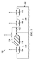
図1は縮尺通りに描かれていない、例示のトランジスタ100の断面図を示す。図1の例では、例示のトランジスタ100はDEMOSトランジスタである。ドレイン領域104及びソース領域106が半導体基材102内に形成される。図1の例では、半導体基板102はシリコン結晶であり、例示のトランジスタ100はn型DEMOSトランジスタであり、ドレイン領域104及びソース領域106はそれぞれ高度にドープされたn型領域である。ソース領域106は軽くドープされたp型ウェル108内に形成され、ドレイン領域104は軽くドープされたn型領域110を介して拡張される。
FIG. 1 shows a cross-sectional view of an
半導体基体102上に誘電体層112が形成される。誘電体層112は、通常、二酸化シリコンであり、誘電体層112はゲート酸化物層112と呼ばれる。ゲート酸化物層112の上にゲート114が形成される。ゲート114は、ポリシリコンを含み得る。酸化物領域116が、半導体基体102の上及び中に成長される。酸化物領域116は、ドレイン領域104に近接しており、ゲート114の下にあり、酸化物領域116は誘電体層112よりも厚い。酸化物領域116は二酸化シリコンを含み得る。酸化物領域116の存在は、ゲート114にリフトアップを提供する。高度にドープされたp型領域118が、例示のトランジスタ100のボディコンタクトとして機能する。
The
例示のトランジスタ100がONであるとき、ゲート114の下のチャネルが反転モードになるように、多数キャリアのチャネル電流(例えば、n型チャネルのための電子)が、ソース領域106からドレイン領域104に流れる。酸化物領域116の存在は、チャネル電流の経路に影響を及ぼす。酸化物領域116のチャネル内への比較的大きな深さは、チャネル電流の多数キャリアを、酸化物領域116の下方及びドレイン領域104に向かって移動することにつれて加速させる。多数キャリアの加速は、例示のトランジスタ100の固有抵抗を減少させるのに役立つ。
Multi-carrier channel currents (eg, electrons for n-type channels) are transferred from the
酸化物領域116は、二重拡散金属酸化物半導体(DMOS)トランジスタなどの他のタイプのトランジスタ、並びに他のタイプの横方向又は垂直トランジスタに用いることができる。図1には示されていないが、他の半導体デバイスが、半導体基板102内に形成され得、様々な回路を実現するために、例示のトランジスタ100に結合され得る。他の半導体デバイスが例示のトランジスタ100と統合されるある実施例では、例示のトランジスタ100の周囲にシリコントレンチアイソレーション(STI)領域が形成されて、他の半導体デバイスからの電気的隔離を提供する。
The
図2は、実施例に従ったプロセスフローの一部の間形成された半導体基体102及びいくつかの層の断面図(縮尺通りに描かれていない)を示す。半導体基材102の上に犠牲誘電体層204が形成される。シリコン技術において、犠牲誘電体層204は典型的には二酸化シリコンを含み、犠牲酸化物層204と呼ばれる。典型的にはシリコン窒化物である障壁層206が、犠牲酸化物層204上に堆積される。底部反射防止コーティング(BARC)208が障壁層206上に堆積され、フォトレジスト層210がBARC208上に堆積される。
FIG. 2 shows a cross-sectional view (not drawn to scale) of the
フォトレジスト層210は、マスク(図示せず)によって画定される照明パターンに従って放射に曝される。フォトレジスト層210上に照射されるパターンは、図1の酸化物領域116を成長させるための開口を画定する。図2の例では、矢印212などの矢印が放射を絵で表す。いくつかの実施例では、放射は、例えば、248nmの波長、又は、アルゴンフッ化物エキシマーレーザーソースの場合の193nmの波長など、深紫外線(DUV)領域にあってもよい。プロセス技術ノードがより小さなサイズに移ると、実施例は、反射性マスク(図示せず)とともに用いられる極紫外線(EUC)レーザーなど、他のタイプの照明源及びマスクを利用することもできる。
The
図2は、半導体基体102の内部及び上に形成された全ての特徴を示すものではない。例えば、半導体基材102内及び半導体基材102上に形成される様々なデバイスを電気的に絶縁するために、埋め込み層及びSTI領域が形成されてもよい。
FIG. 2 does not show all the features formed inside and on the
図3は、実施例に従って、開口302を提供するためにエッチングが行われた後、図2の層を備える、シリコン基板102の断面図(縮尺通りに描かれていない)を示す。エッチングは、プラズマ反応性イオンエッチングを含み得る。プラズマRIEは、酸素(O2)、キャリア気体(例えば、アルゴン)、又は、x=1又は2、y=0、1、2、3、又は4、及びz=1、2、3、又は4の化学量論CxHyFzを有する炭素(C)、水素(H)、及びフッ素(F)を含むフッ化炭素の気体混合物において成され得る。
FIG. 3 shows a cross-sectional view (not drawn to scale) of a
図4は、実施例に従って、酸化物領域116が成長された図3の層を備えるシリコン基板102の断面図(縮尺通りに描かれていない)を示す。いくつかの実施例では、酸化物領域116は、少なくとも400オングストローム、例えば、400オングストロームから4000オングストロームの範囲、の厚みを有し得る。半導体基材102は、酸化物領域116を成長させるため、或る雰囲気酸化剤に曝される。ある実施例では、雰囲気酸化は、酸素及び/又は水蒸気を用いて熱炉酸化プロセスにおいて行われる。幾つかの実施例では、半導体基質102は、例えば950℃〜l000℃の範囲など、900℃を超える温度で、酸素及び/又は水蒸気に曝される。
FIG. 4 shows a cross-sectional view (not drawn to scale) of a
障壁層206の厚みは、障壁層206の下の横方向酸化のため、「バーズビーク(bird’s beak)」(「バーズビーク(birds beak)」とも呼ばれる)形状の酸化物領域116の形成に影響を提供する。障壁層206の厚みは、300オングストローム〜1000オングストロームの厚みを有し得る。いくつかの実施例では、障壁層206は約950オングストロームの厚さであり得る。
The thickness of the
酸化物領域116を形成した後、図4に示す半導体基材102の上の様々な層(酸化物領域116を除く)が除去され、続いて追加のプロセス工程を行って、例えば図1の例示のトランジスタ100などのトランジスタを製造する。例えば、ドーパントを注入して、軽くドープされたn型領域110、ドレイン領域104、及びソース領域106が形成され得る。犠牲酸化物層204は、ゲート酸化物層112を成長させる前に除去され、ゲート114はゲート酸化物層112の上に形成される。
After forming the
図5は、例示のプロセスフロー500を示す。例示のプロセスフロー500は、工程501において、1つ又はそれ以上のSTI領域を形成すること、工程502において、半導体基板(例えば、半導体基板102)上に第1の誘電体層を形成すること、工程504において、第1の誘電体層上に障壁層206(例えば、シリコン窒化物層)を堆積すること、工程506において、反射防止コーティング(例えば、BARC208)を堆積すること、工程508において、フォトレジスト層(例えば、フォトレジスト層210)を堆積すること、工程510において、フォトレジスト層におけるパターンを放射に曝すこと、工程512において、フォトレジスト層における開口を提供するためパターンに従ってフォトレジスト層をエッチングすること、工程514において、フォトレジスト層の開口の下の反射防止コーティングの一部をエッチングすること、工程516において、第1の誘電体層の一部を露出させるため障壁層の一部をエッチングすること、工程518において、開口の下の障壁層の一部をエッチングした後、雰囲気酸化剤を提供すること、工程520において、雰囲気酸化剤を提供した後、障壁層を除去すること、工程522において、障壁層を除去した後、ドーパントを半導体基板に注入すること(例えば、ドレイン領域104又はソース領域106を形成するため)、工程524において、ドーパントを半導体基板に注入した後、第1の誘電体層を除去すること、工程526において、第1の誘電体層を除去した後、第2の誘電体層(例えば、ゲート酸化物層112)を形成することを含む。
FIG. 5 shows an
実施例に従ったトランジスタ(例えば、プロセスフロー500)を製造する際の処理工程は標準のプロセスフロー、例えば、標準のBiCMOSプロセス、又は線形BiCMOS(LBC)プロセスに組み込むことができる。追加の処理工程が、図5に関して記載された処理工程などの一実施例における処理工程の前後に実行されてもよい。例えば、埋め込み領域を形成するための半導体基板102へのドーパント注入は、プロセスフロー500より先に行われてもよい。別の例として、エピタキシャル層が、プロセスフロー500の前に半導体基材102上に成長されてもよい。
The processing steps in manufacturing a transistor according to an embodiment (eg, process flow 500) can be incorporated into a standard process flow, eg, a standard BiCMOS process, or a linear BiCMOS (LBC) process. Additional treatment steps may be performed before and after the treatment steps in one embodiment, such as the treatment steps described with respect to FIG. For example, the dopant injection into the
複数デバイスをウェハ上に製造する場合、図5に示される工程の一部又は全部が繰り返され得る。例えば、工程526(及び工程526に関連する工程)は、それぞれのゲート酸化物層に対して異なる厚みを有する複数のトランジスタを製造するために繰り返され得る。具体例として、工程526の反復で形成される誘電体層が、約40オングストロームの厚みを有し得、そのため、約40オングストロームのゲート酸化物層を有する1つ又はそれ以上のトランジスタが製造される。工程526の別の反復において、誘電体層が約100オングストロームの厚みを有し得、そのため、1つ又はそれ以上のトランジスタが、より高い動作電圧に適した約100オングストロームのゲート酸化物層を有するように製造される。
When manufacturing multiple devices on a wafer, some or all of the steps shown in FIG. 5 can be repeated. For example, step 526 (and the steps associated with step 526) can be repeated to produce a plurality of transistors having different thicknesses for each gate oxide layer. As a specific example, the dielectric layer formed by repeating
図6は、2つの例示のトランジスタの断面図(一定の縮尺で描かれてはいない)を示す。図6は、例示のトランジスタ100が形成されるが、高度にドープされたp型領域118(ボディコンタクト)が示されていない、半導体基板602を示す。半導体基板602内に形成されるのは、例示のトランジスタ600(そのボディコンタクトは図示しない)である。STI領域601が、例示のトランジスタ600から例示のトランジスタ100を隔離する。
FIG. 6 shows a cross section of two exemplary transistors (not drawn to a constant scale). FIG. 6 shows a semiconductor substrate 602 in which the
例示のトランジスタ600は、ドレイン領域604及びソース領域606を含む。図6の実施例において、例示のトランジスタ600はn型DMOSトランジスタであり、ドレイン領域604及びソース領域606は、各々、高ドープされたn型領域である。ソース領域606は軽くドープされたp型ウェル608内に形成され、ドレイン領域604は軽くドープされたn型領域610を介して拡長される。
The illustrated
半導体基板602上にゲート酸化物層(誘電体層)612が形成される。ゲート酸化物層612の上にゲート614が形成される。半導体基板602上及びその中に酸化物領域616が成長される。酸化物領域616は、ドレイン領域604に近接しており、ゲート614の下にあり、酸化物領域616は、ゲート酸化物層612よりも厚い。ゲート酸化物層612はゲート酸化物層112よりも厚く、その結果、例示のトランジスタ600は例示のトランジスタ100よりも高い動作電圧に耐えることができる。
A gate oxide layer (dielectric layer) 612 is formed on the semiconductor substrate 602. A
本発明の特許請求の範囲内で、説明した例示の実施例に改変が成され得、他の実施例が可能である。 Within the scope of the claims of the present invention, modifications can be made to the illustrated examples described, and other examples are possible.
Claims (20)
半導体基板上に第1の誘電体層を形成すること、
前記第1の誘電体層上に障壁層を堆積すること、
前記障壁層上に反射防止コーティングを堆積すること、
フォトレジスト層を堆積すること、
前記フォトレジスト層におけるパターンを放射に曝すこと、
前記フォトレジスト層に開口を提供するために、前記パターンに従って前記フォトレジスト層をエッチングすること、
前記フォトレジスト層における前記開口の下の反射防止コーティングの一部をエッチングすること、
前記第1の誘電体層の一部を露出させるため、前記開口の下の前記障壁層の一部をエッチングすること、
酸化物領域を成長させるため、前記開口の下の前記障壁層の前記一部をエッチした後、雰囲気酸化剤を提供すること、
前記雰囲気酸化剤を提供した後、前記障壁層を除去すること、
前記障壁層を取り除いた後、前記半導体基板内にドーパントを注入すること、
前記半導体基板にドーパントを注入した後、前記第1の誘電体層を除去すること、
前記第1の誘電体層を除去した後、第2の誘電体層を形成することであって、前記酸化物領域が前記第2の誘電体層より厚くなるように成長されること、
を含む、方法。 It ’s a method of manufacturing transistors.
Forming a first dielectric layer on a semiconductor substrate,
Placing a barrier layer on the first dielectric layer,
Placing an anti-reflective coating on the barrier layer,
Placing a photoresist layer,
Exposing the pattern in the photoresist layer to radiation,
Etching the photoresist layer according to the pattern to provide openings in the photoresist layer.
Etching a portion of the antireflection coating under the opening in the photoresist layer,
Etching a portion of the barrier layer below the opening to expose a portion of the first dielectric layer.
To provide an atmospheric oxidant after etching the portion of the barrier layer below the opening to grow the oxide region.
After providing the atmospheric oxidant, removing the barrier layer,
After removing the barrier layer, injecting a dopant into the semiconductor substrate,
After injecting the dopant into the semiconductor substrate, removing the first dielectric layer,
By forming the second dielectric layer after removing the first dielectric layer, the oxide region is grown to be thicker than the second dielectric layer.
Including methods.
シャロートレンチアイソレーション(STI)領域を形成すること、及び
前記第2の誘電体層よりもより厚い、第3の誘電体層を形成すること、
を更に含む、方法。 The method of claim 1
Forming a shallow trench isolation (STI) region and forming a third dielectric layer that is thicker than the second dielectric layer.
A method that further comprises.
前記第2の誘電体層上に第2のフォトレジスト層を堆積すること、
前記第2のフォトレジスト層における第2のパターンを放射に曝すこと、
前記第2のフォトレジスト層に開口を提供するため、前記第2のパターンに従って前記第2のフォトレジスト層をエッチングすること、
前記第2のフォトレジスト層の前記開口を介して、第2の誘電体層上に導電性材料を堆積すること、
を更に含む、方法。 The method of claim 1
To deposit a second photoresist layer on the second dielectric layer,
Exposing the second pattern in the second photoresist layer to radiation,
Etching the second photoresist layer according to the second pattern to provide an opening in the second photoresist layer.
To deposit a conductive material on the second dielectric layer through the opening of the second photoresist layer.
A method that further comprises.
半導体基板上に犠牲酸化物層を形成すること、
前記犠牲酸化物層上にシリコン窒化物層を堆積すること、
前記シリコン窒化物層上に反射防止コーティングを堆積すること、
フォトレジスト層を堆積すること、
前記フォトレジスト層におけるパターンを放射に曝すこと、
前記フォトレジスト層内に開口を提供するため、前記パターンに従って前記フォトレジスト層をエッチングすること、
前記開口の下の前記反射性防止コーティングの一部をエッチングすること、
前記犠牲酸化物層の一部を露出させるため、前記開口の下の前記シリコン窒化物層の一部をエッチングすること、
前記犠牲酸化物層の前記露出された部分上に酸化物領域を成長させること、
前記酸化物領域を成長させた後、前記シリコン窒化物層を取り除くこと、
前記シリコン窒化物層を除去した後、前記半導体基板にドーパントを注入すること、
前記半導体基板にドーパントを注入した後、前記犠牲酸化物層を取り除くこと、及び
前記犠牲酸化物層を除去した後に前記半導体基板上にゲート酸化物層を形成することであって、前記酸化物領域が、前記ゲート酸化物層の厚みよりも厚く成長されること、
を含む、方法。 It ’s a method of manufacturing transistors.
Forming a sacrificial oxide layer on a semiconductor substrate,
Placing a silicon nitride layer on the sacrificial oxide layer,
Placing an antireflection coating on the silicon nitride layer,
Placing a photoresist layer,
Exposing the pattern in the photoresist layer to radiation,
Etching the photoresist layer according to the pattern to provide an opening in the photoresist layer.
Etching a portion of the anti-reflective coating under the opening,
Etching a portion of the silicon nitride layer under the opening to expose a portion of the sacrificial oxide layer.
Growing an oxide region on the exposed portion of the sacrificial oxide layer,
After growing the oxide region, removing the silicon nitride layer,
After removing the silicon nitride layer, the dopant is injected into the semiconductor substrate.
After injecting a dopant into the semiconductor substrate, the sacrificial oxide layer is removed, and after the sacrificial oxide layer is removed, a gate oxide layer is formed on the semiconductor substrate. However, it grows thicker than the thickness of the gate oxide layer.
Including methods.
半導体基板上に犠牲酸化物層を形成すること、
前記犠牲酸化物層上にシリコン窒化物層を堆積すること、
フォトレジスト層を堆積すること、
前記フォトレジスト層内におけるパターンを放射に曝すこと、
前記フォトレジスト層に開口を提供するため、前記パターンに従って前記フォトレジスト層をエッチングすること、
前記犠牲酸化物層の一部を露出させるため、前記開口の下の前記シリコン窒化物層の一部をエッチングすること、
前記犠牲酸化物層の前記露出された部分上に少なくとも400オングストロームの厚さの酸化物領域を成長させること、
前記酸化物領域を成長させた後、前記シリコン窒化物層を取り除くこと、
前記半導体基板内にドレイン領域を形成するため、前記シリコン窒化物層を除去した後に半導体基板内にドーパントを注入すること、
前記半導体基板にドーパントを注入した後に前記犠牲酸化物層を除去すること、及び
前記犠牲酸化物層を除去した後に半導体基板上にゲート酸化物層を形成すること、
を含み、
前記ゲート酸化物層が400オングストローム未満の厚みを有する、
方法。 It ’s a method of manufacturing transistors.
Forming a sacrificial oxide layer on a semiconductor substrate,
Placing a silicon nitride layer on the sacrificial oxide layer,
Placing a photoresist layer,
Exposing the pattern in the photoresist layer to radiation,
Etching the photoresist layer according to the pattern to provide openings in the photoresist layer.
Etching a portion of the silicon nitride layer under the opening to expose a portion of the sacrificial oxide layer.
Growing an oxide region with a thickness of at least 400 angstroms on the exposed portion of the sacrificial oxide layer.
After growing the oxide region, removing the silicon nitride layer,
In order to form a drain region in the semiconductor substrate, the dopant is injected into the semiconductor substrate after removing the silicon nitride layer.
Removing the sacrificial oxide layer after injecting a dopant into the semiconductor substrate, and forming a gate oxide layer on the semiconductor substrate after removing the sacrificial oxide layer.
Including
The gate oxide layer has a thickness of less than 400 angstroms.
Method.
Applications Claiming Priority (3)
| Application Number | Priority Date | Filing Date | Title |
|---|---|---|---|
| US15/944,550 | 2018-04-03 | ||
| US15/944,550 US10566200B2 (en) | 2018-04-03 | 2018-04-03 | Method of fabricating transistors, including ambient oxidizing after etchings into barrier layers and anti-reflecting coatings |
| PCT/US2019/025599 WO2019195435A1 (en) | 2018-04-03 | 2019-04-03 | Method of fabricating transistors |
Publications (2)
| Publication Number | Publication Date |
|---|---|
| JP2021521629A true JP2021521629A (en) | 2021-08-26 |
| JPWO2019195435A5 JPWO2019195435A5 (en) | 2022-04-08 |
Family
ID=68055429
Family Applications (1)
| Application Number | Title | Priority Date | Filing Date |
|---|---|---|---|
| JP2020554400A Pending JP2021521629A (en) | 2018-04-03 | 2019-04-03 | How to make a transistor |
Country Status (5)
| Country | Link |
|---|---|
| US (1) | US10566200B2 (en) |
| EP (1) | EP3776637A4 (en) |
| JP (1) | JP2021521629A (en) |
| CN (1) | CN112074932A (en) |
| WO (1) | WO2019195435A1 (en) |
Families Citing this family (1)
| Publication number | Priority date | Publication date | Assignee | Title |
|---|---|---|---|---|
| US11227926B2 (en) * | 2020-06-01 | 2022-01-18 | Nanya Technology Corporation | Semiconductor device and method for fabricating the same |
Citations (9)
| Publication number | Priority date | Publication date | Assignee | Title |
|---|---|---|---|---|
| JPH1167904A (en) * | 1997-08-15 | 1999-03-09 | Hitachi Ltd | Manufacture of semiconductor integrated circuit device |
| JP2000353804A (en) * | 1999-06-11 | 2000-12-19 | Mitsubishi Electric Corp | Semiconductor device and manufacture of the same |
| JP2001196578A (en) * | 1999-10-29 | 2001-07-19 | Sanyo Electric Co Ltd | Semiconductor device and manufacturing method therefor |
| JP2004200359A (en) * | 2002-12-18 | 2004-07-15 | Ricoh Co Ltd | Semiconductor device and method of manufacturing the same |
| JP2005123314A (en) * | 2003-10-15 | 2005-05-12 | Semiconductor Leading Edge Technologies Inc | Pattern forming method |
| JP2009170552A (en) * | 2008-01-11 | 2009-07-30 | Fuji Electric Device Technology Co Ltd | Semiconductor device and manufacturing method thereof |
| JP2013080817A (en) * | 2011-10-04 | 2013-05-02 | Fujitsu Semiconductor Ltd | Semiconductor device and semiconductor device manufacturing method |
| JP2014053523A (en) * | 2012-09-10 | 2014-03-20 | Renesas Electronics Corp | Semiconductor device and manufacturing method of the same |
| JP2014192361A (en) * | 2013-03-27 | 2014-10-06 | Sharp Corp | Semiconductor device and manufacturing method of the same |
Family Cites Families (11)
| Publication number | Priority date | Publication date | Assignee | Title |
|---|---|---|---|---|
| US4040168A (en) | 1975-11-24 | 1977-08-09 | Rca Corporation | Fabrication method for a dual gate field-effect transistor |
| US5512495A (en) * | 1994-04-08 | 1996-04-30 | Texas Instruments Incorporated | Method of manufacturing extended drain resurf lateral DMOS devices |
| US6121133A (en) * | 1997-08-22 | 2000-09-19 | Micron Technology, Inc. | Isolation using an antireflective coating |
| KR100867574B1 (en) * | 2002-05-09 | 2008-11-10 | 페어차일드코리아반도체 주식회사 | Power device and method for manufacturing the same |
| JP2005236281A (en) * | 2004-01-29 | 2005-09-02 | Rohm & Haas Electronic Materials Llc | T-gate formation |
| DE102004031741B4 (en) | 2004-06-30 | 2010-04-01 | Qimonda Ag | Method for producing a contact arrangement for field effect transistor structures with gate electrodes with a metal layer and use of the method for producing field effect transistor arrangements in a cell array |
| KR20060070334A (en) | 2004-12-20 | 2006-06-23 | 삼성전자주식회사 | Method for manufacturing thin film transistor array panel |
| CN101218675A (en) * | 2005-07-07 | 2008-07-09 | 密克罗奇普技术公司 | ESD structure having different thickness gate oxides |
| US20070018199A1 (en) | 2005-07-20 | 2007-01-25 | Cree, Inc. | Nitride-based transistors and fabrication methods with an etch stop layer |
| EP2244299A1 (en) * | 2009-04-22 | 2010-10-27 | STMicroelectronics S.r.l. | MOS transistor for power applications and corresponding integrated circuit and manufacturing method |
| US9218978B1 (en) * | 2015-03-09 | 2015-12-22 | Cypress Semiconductor Corporation | Method of ONO stack formation |
-
2018
- 2018-04-03 US US15/944,550 patent/US10566200B2/en active Active
-
2019
- 2019-04-03 CN CN201980029913.7A patent/CN112074932A/en active Pending
- 2019-04-03 JP JP2020554400A patent/JP2021521629A/en active Pending
- 2019-04-03 EP EP19781451.0A patent/EP3776637A4/en not_active Withdrawn
- 2019-04-03 WO PCT/US2019/025599 patent/WO2019195435A1/en unknown
Patent Citations (11)
| Publication number | Priority date | Publication date | Assignee | Title |
|---|---|---|---|---|
| JPH1167904A (en) * | 1997-08-15 | 1999-03-09 | Hitachi Ltd | Manufacture of semiconductor integrated circuit device |
| JP2000353804A (en) * | 1999-06-11 | 2000-12-19 | Mitsubishi Electric Corp | Semiconductor device and manufacture of the same |
| JP2001196578A (en) * | 1999-10-29 | 2001-07-19 | Sanyo Electric Co Ltd | Semiconductor device and manufacturing method therefor |
| JP2004200359A (en) * | 2002-12-18 | 2004-07-15 | Ricoh Co Ltd | Semiconductor device and method of manufacturing the same |
| JP2005123314A (en) * | 2003-10-15 | 2005-05-12 | Semiconductor Leading Edge Technologies Inc | Pattern forming method |
| JP2009170552A (en) * | 2008-01-11 | 2009-07-30 | Fuji Electric Device Technology Co Ltd | Semiconductor device and manufacturing method thereof |
| JP2013080817A (en) * | 2011-10-04 | 2013-05-02 | Fujitsu Semiconductor Ltd | Semiconductor device and semiconductor device manufacturing method |
| JP2014053523A (en) * | 2012-09-10 | 2014-03-20 | Renesas Electronics Corp | Semiconductor device and manufacturing method of the same |
| CN103681862A (en) * | 2012-09-10 | 2014-03-26 | 瑞萨电子株式会社 | Semiconductor device and method of manufacturing same |
| US9099548B2 (en) * | 2012-09-10 | 2015-08-04 | Renesas Electronics Corporation | Semiconductor device and method of manufacturing same |
| JP2014192361A (en) * | 2013-03-27 | 2014-10-06 | Sharp Corp | Semiconductor device and manufacturing method of the same |
Also Published As
| Publication number | Publication date |
|---|---|
| US10566200B2 (en) | 2020-02-18 |
| EP3776637A1 (en) | 2021-02-17 |
| CN112074932A (en) | 2020-12-11 |
| US20190304786A1 (en) | 2019-10-03 |
| WO2019195435A1 (en) | 2019-10-10 |
| EP3776637A4 (en) | 2021-05-05 |
Similar Documents
| Publication | Publication Date | Title |
|---|---|---|
| EP0363944B1 (en) | Method of manufacturing a semiconductor device having a silicon carbide layer | |
| EP0036573A2 (en) | Method for making a polysilicon conductor structure | |
| US6413881B1 (en) | Process for forming thin gate oxide with enhanced reliability by nitridation of upper surface of gate of oxide to form barrier of nitrogen atoms in upper surface region of gate oxide, and resulting product | |
| US7785974B2 (en) | Methods of employing a thin oxide mask for high dose implants | |
| CN103137618B (en) | Locally carrier lifetime reduces | |
| TW479281B (en) | A silicon-germanium transistor and associated methods | |
| KR100763333B1 (en) | Method of forming an isolation layer of a semiconductor device | |
| US6358865B2 (en) | Oxidation of silicon using fluorine implant | |
| JP2004134719A (en) | Manufacturing method for semiconductor element | |
| JP2021521629A (en) | How to make a transistor | |
| JP3874716B2 (en) | Manufacturing method of semiconductor device | |
| US5208181A (en) | Locos isolation scheme for small geometry or high voltage circuit | |
| US20170309484A1 (en) | Carbon Vacancy Defect Reduction Method for SiC | |
| US6787879B1 (en) | Interfacial oxide in a transistor | |
| US20100032813A1 (en) | Ic formed with densified chemical oxide layer | |
| KR100682178B1 (en) | Method for manufacturing CMOS | |
| US20150311327A1 (en) | Itc-igbt and manufacturing method therefor | |
| KR20050069170A (en) | Method for manufacturing mos transistor | |
| US11869986B2 (en) | Vertical deep trench and deep trench island based deep n-type well diode and diode triggered protection device | |
| KR930008873B1 (en) | Device seperating method of semiconductor apparatus | |
| KR100451768B1 (en) | Method for fabricating gate dielectric of semiconductor device | |
| KR101068150B1 (en) | Method for forming contact plug of semiconductor device | |
| KR100448591B1 (en) | Method of manufacturing a transistor in a semiconductor | |
| JP2013168562A (en) | Semiconductor device manufacturing method | |
| KR100481396B1 (en) | Method of manufacturing a semiconductor device |
Legal Events
| Date | Code | Title | Description |
|---|---|---|---|
| A521 | Request for written amendment filed |
Free format text: JAPANESE INTERMEDIATE CODE: A821 Effective date: 20201005 |
|
| A711 | Notification of change in applicant |
Free format text: JAPANESE INTERMEDIATE CODE: A711 Effective date: 20210218 |
|
| A521 | Request for written amendment filed |
Free format text: JAPANESE INTERMEDIATE CODE: A523 Effective date: 20210323 |
|
| A521 | Request for written amendment filed |
Free format text: JAPANESE INTERMEDIATE CODE: A523 Effective date: 20210602 |
|
| A521 | Request for written amendment filed |
Free format text: JAPANESE INTERMEDIATE CODE: A523 Effective date: 20220331 |
|
| A625 | Written request for application examination (by other person) |
Free format text: JAPANESE INTERMEDIATE CODE: A625 Effective date: 20220331 |
|
| RD01 | Notification of change of attorney |
Free format text: JAPANESE INTERMEDIATE CODE: A7421 Effective date: 20220518 |
|
| A131 | Notification of reasons for refusal |
Free format text: JAPANESE INTERMEDIATE CODE: A131 Effective date: 20230322 |
|
| A977 | Report on retrieval |
Free format text: JAPANESE INTERMEDIATE CODE: A971007 Effective date: 20230309 |
|
| A601 | Written request for extension of time |
Free format text: JAPANESE INTERMEDIATE CODE: A601 Effective date: 20230622 |
|
| A601 | Written request for extension of time |
Free format text: JAPANESE INTERMEDIATE CODE: A601 Effective date: 20230822 |
|
| A02 | Decision of refusal |
Free format text: JAPANESE INTERMEDIATE CODE: A02 Effective date: 20231114 |