EP0036573A2 - Method for making a polysilicon conductor structure - Google Patents
Method for making a polysilicon conductor structure Download PDFInfo
- Publication number
- EP0036573A2 EP0036573A2 EP81101830A EP81101830A EP0036573A2 EP 0036573 A2 EP0036573 A2 EP 0036573A2 EP 81101830 A EP81101830 A EP 81101830A EP 81101830 A EP81101830 A EP 81101830A EP 0036573 A2 EP0036573 A2 EP 0036573A2
- Authority
- EP
- European Patent Office
- Prior art keywords
- silicon
- polycrystalline silicon
- silicon dioxide
- layer
- polycrystalline
- Prior art date
- Legal status (The legal status is an assumption and is not a legal conclusion. Google has not performed a legal analysis and makes no representation as to the accuracy of the status listed.)
- Granted
Links
- 229910021420 polycrystalline silicon Inorganic materials 0.000 title claims abstract description 71
- 238000000034 method Methods 0.000 title claims abstract description 46
- 239000004020 conductor Substances 0.000 title claims abstract description 13
- 229920005591 polysilicon Polymers 0.000 title abstract description 8
- VYPSYNLAJGMNEJ-UHFFFAOYSA-N Silicium dioxide Chemical compound O=[Si]=O VYPSYNLAJGMNEJ-UHFFFAOYSA-N 0.000 claims abstract description 105
- 235000012239 silicon dioxide Nutrition 0.000 claims abstract description 52
- 239000000377 silicon dioxide Substances 0.000 claims abstract description 52
- 229910052710 silicon Inorganic materials 0.000 claims abstract description 22
- 239000010703 silicon Substances 0.000 claims abstract description 22
- XUIMIQQOPSSXEZ-UHFFFAOYSA-N Silicon Chemical compound [Si] XUIMIQQOPSSXEZ-UHFFFAOYSA-N 0.000 claims abstract description 19
- 238000001020 plasma etching Methods 0.000 claims abstract description 17
- 230000005669 field effect Effects 0.000 claims abstract description 15
- 239000011248 coating agent Substances 0.000 claims abstract description 11
- 238000000576 coating method Methods 0.000 claims abstract description 11
- 239000000758 substrate Substances 0.000 claims abstract description 11
- 239000012212 insulator Substances 0.000 claims abstract description 10
- 230000000873 masking effect Effects 0.000 claims abstract description 7
- 230000015572 biosynthetic process Effects 0.000 claims abstract description 6
- QVGXLLKOCUKJST-UHFFFAOYSA-N atomic oxygen Chemical compound [O] QVGXLLKOCUKJST-UHFFFAOYSA-N 0.000 claims description 7
- 239000001301 oxygen Substances 0.000 claims description 7
- 229910052760 oxygen Inorganic materials 0.000 claims description 7
- 238000000151 deposition Methods 0.000 claims description 5
- 239000003989 dielectric material Substances 0.000 claims description 2
- 230000001590 oxidative effect Effects 0.000 claims 3
- 230000003647 oxidation Effects 0.000 abstract description 13
- 238000007254 oxidation reaction Methods 0.000 abstract description 13
- 230000005856 abnormality Effects 0.000 abstract description 4
- 238000002955 isolation Methods 0.000 description 8
- 238000009792 diffusion process Methods 0.000 description 7
- 238000005530 etching Methods 0.000 description 7
- 238000005468 ion implantation Methods 0.000 description 6
- 229910052581 Si3N4 Inorganic materials 0.000 description 5
- HQVNEWCFYHHQES-UHFFFAOYSA-N silicon nitride Chemical compound N12[Si]34N5[Si]62N3[Si]51N64 HQVNEWCFYHHQES-UHFFFAOYSA-N 0.000 description 5
- IJGRMHOSHXDMSA-UHFFFAOYSA-N Atomic nitrogen Chemical compound N#N IJGRMHOSHXDMSA-UHFFFAOYSA-N 0.000 description 4
- 239000000126 substance Substances 0.000 description 4
- 230000008021 deposition Effects 0.000 description 3
- 238000001459 lithography Methods 0.000 description 3
- QGZKDVFQNNGYKY-UHFFFAOYSA-N Ammonia Chemical compound N QGZKDVFQNNGYKY-UHFFFAOYSA-N 0.000 description 2
- VEXZGXHMUGYJMC-UHFFFAOYSA-N Hydrochloric acid Chemical compound Cl VEXZGXHMUGYJMC-UHFFFAOYSA-N 0.000 description 2
- IXCSERBJSXMMFS-UHFFFAOYSA-N hydrogen chloride Substances Cl.Cl IXCSERBJSXMMFS-UHFFFAOYSA-N 0.000 description 2
- 229910000041 hydrogen chloride Inorganic materials 0.000 description 2
- 239000000463 material Substances 0.000 description 2
- 229910021421 monocrystalline silicon Inorganic materials 0.000 description 2
- 229910052757 nitrogen Inorganic materials 0.000 description 2
- PNEYBMLMFCGWSK-UHFFFAOYSA-N Alumina Chemical compound [O-2].[O-2].[O-2].[Al+3].[Al+3] PNEYBMLMFCGWSK-UHFFFAOYSA-N 0.000 description 1
- ZOXJGFHDIHLPTG-UHFFFAOYSA-N Boron Chemical compound [B] ZOXJGFHDIHLPTG-UHFFFAOYSA-N 0.000 description 1
- UFHFLCQGNIYNRP-UHFFFAOYSA-N Hydrogen Chemical compound [H][H] UFHFLCQGNIYNRP-UHFFFAOYSA-N 0.000 description 1
- BLRPTPMANUNPDV-UHFFFAOYSA-N Silane Chemical compound [SiH4] BLRPTPMANUNPDV-UHFFFAOYSA-N 0.000 description 1
- VVTRNRPINJRHBQ-UHFFFAOYSA-N [Cl].[Ar] Chemical compound [Cl].[Ar] VVTRNRPINJRHBQ-UHFFFAOYSA-N 0.000 description 1
- PQHYVQFXKYEWQN-UHFFFAOYSA-N [N].[O].O Chemical compound [N].[O].O PQHYVQFXKYEWQN-UHFFFAOYSA-N 0.000 description 1
- 230000002411 adverse Effects 0.000 description 1
- 229910021529 ammonia Inorganic materials 0.000 description 1
- 238000000137 annealing Methods 0.000 description 1
- 239000012300 argon atmosphere Substances 0.000 description 1
- XKDYZCVIKLTUBO-UHFFFAOYSA-N argon;tetrachloromethane Chemical compound [Ar].ClC(Cl)(Cl)Cl XKDYZCVIKLTUBO-UHFFFAOYSA-N 0.000 description 1
- 239000012298 atmosphere Substances 0.000 description 1
- 229910052796 boron Inorganic materials 0.000 description 1
- 238000005229 chemical vapour deposition Methods 0.000 description 1
- 238000010276 construction Methods 0.000 description 1
- 230000000694 effects Effects 0.000 description 1
- 239000007789 gas Substances 0.000 description 1
- 239000011521 glass Substances 0.000 description 1
- 239000001257 hydrogen Substances 0.000 description 1
- 229910052739 hydrogen Inorganic materials 0.000 description 1
- 239000007943 implant Substances 0.000 description 1
- 239000012535 impurity Substances 0.000 description 1
- 150000002500 ions Chemical class 0.000 description 1
- 230000015654 memory Effects 0.000 description 1
- 238000005272 metallurgy Methods 0.000 description 1
- 239000000203 mixture Substances 0.000 description 1
- 229920002120 photoresistant polymer Polymers 0.000 description 1
- 238000010405 reoxidation reaction Methods 0.000 description 1
- 229910000077 silane Inorganic materials 0.000 description 1
- XUGSDIOYQBRKGF-UHFFFAOYSA-N silicon;hydrochloride Chemical compound [Si].Cl XUGSDIOYQBRKGF-UHFFFAOYSA-N 0.000 description 1
- 241000894007 species Species 0.000 description 1
- XLYOFNOQVPJJNP-UHFFFAOYSA-N water Substances O XLYOFNOQVPJJNP-UHFFFAOYSA-N 0.000 description 1
- 229910001868 water Inorganic materials 0.000 description 1
Images
Classifications
-
- H—ELECTRICITY
- H01—ELECTRIC ELEMENTS
- H01L—SEMICONDUCTOR DEVICES NOT COVERED BY CLASS H10
- H01L29/00—Semiconductor devices adapted for rectifying, amplifying, oscillating or switching, or capacitors or resistors with at least one potential-jump barrier or surface barrier, e.g. PN junction depletion layer or carrier concentration layer; Details of semiconductor bodies or of electrodes thereof ; Multistep manufacturing processes therefor
- H01L29/66—Types of semiconductor device ; Multistep manufacturing processes therefor
- H01L29/66007—Multistep manufacturing processes
- H01L29/66075—Multistep manufacturing processes of devices having semiconductor bodies comprising group 14 or group 13/15 materials
- H01L29/66227—Multistep manufacturing processes of devices having semiconductor bodies comprising group 14 or group 13/15 materials the devices being controllable only by the electric current supplied or the electric potential applied, to an electrode which does not carry the current to be rectified, amplified or switched, e.g. three-terminal devices
- H01L29/66409—Unipolar field-effect transistors
- H01L29/66477—Unipolar field-effect transistors with an insulated gate, i.e. MISFET
- H01L29/66568—Lateral single gate silicon transistors
- H01L29/66575—Lateral single gate silicon transistors where the source and drain or source and drain extensions are self-aligned to the sides of the gate
-
- H—ELECTRICITY
- H01—ELECTRIC ELEMENTS
- H01L—SEMICONDUCTOR DEVICES NOT COVERED BY CLASS H10
- H01L21/00—Processes or apparatus adapted for the manufacture or treatment of semiconductor or solid state devices or of parts thereof
- H01L21/02—Manufacture or treatment of semiconductor devices or of parts thereof
- H01L21/027—Making masks on semiconductor bodies for further photolithographic processing not provided for in group H01L21/18 or H01L21/34
- H01L21/033—Making masks on semiconductor bodies for further photolithographic processing not provided for in group H01L21/18 or H01L21/34 comprising inorganic layers
-
- H—ELECTRICITY
- H01—ELECTRIC ELEMENTS
- H01L—SEMICONDUCTOR DEVICES NOT COVERED BY CLASS H10
- H01L21/00—Processes or apparatus adapted for the manufacture or treatment of semiconductor or solid state devices or of parts thereof
- H01L21/02—Manufacture or treatment of semiconductor devices or of parts thereof
- H01L21/04—Manufacture or treatment of semiconductor devices or of parts thereof the devices having at least one potential-jump barrier or surface barrier, e.g. PN junction, depletion layer or carrier concentration layer
- H01L21/18—Manufacture or treatment of semiconductor devices or of parts thereof the devices having at least one potential-jump barrier or surface barrier, e.g. PN junction, depletion layer or carrier concentration layer the devices having semiconductor bodies comprising elements of Group IV of the Periodic System or AIIIBV compounds with or without impurities, e.g. doping materials
- H01L21/30—Treatment of semiconductor bodies using processes or apparatus not provided for in groups H01L21/20 - H01L21/26
- H01L21/31—Treatment of semiconductor bodies using processes or apparatus not provided for in groups H01L21/20 - H01L21/26 to form insulating layers thereon, e.g. for masking or by using photolithographic techniques; After treatment of these layers; Selection of materials for these layers
- H01L21/3205—Deposition of non-insulating-, e.g. conductive- or resistive-, layers on insulating layers; After-treatment of these layers
- H01L21/321—After treatment
-
- H—ELECTRICITY
- H01—ELECTRIC ELEMENTS
- H01L—SEMICONDUCTOR DEVICES NOT COVERED BY CLASS H10
- H01L21/00—Processes or apparatus adapted for the manufacture or treatment of semiconductor or solid state devices or of parts thereof
- H01L21/70—Manufacture or treatment of devices consisting of a plurality of solid state components formed in or on a common substrate or of parts thereof; Manufacture of integrated circuit devices or of parts thereof
- H01L21/77—Manufacture or treatment of devices consisting of a plurality of solid state components or integrated circuits formed in, or on, a common substrate
- H01L21/78—Manufacture or treatment of devices consisting of a plurality of solid state components or integrated circuits formed in, or on, a common substrate with subsequent division of the substrate into plural individual devices
- H01L21/82—Manufacture or treatment of devices consisting of a plurality of solid state components or integrated circuits formed in, or on, a common substrate with subsequent division of the substrate into plural individual devices to produce devices, e.g. integrated circuits, each consisting of a plurality of components
- H01L21/822—Manufacture or treatment of devices consisting of a plurality of solid state components or integrated circuits formed in, or on, a common substrate with subsequent division of the substrate into plural individual devices to produce devices, e.g. integrated circuits, each consisting of a plurality of components the substrate being a semiconductor, using silicon technology
- H01L21/8232—Field-effect technology
- H01L21/8234—MIS technology, i.e. integration processes of field effect transistors of the conductor-insulator-semiconductor type
-
- Y—GENERAL TAGGING OF NEW TECHNOLOGICAL DEVELOPMENTS; GENERAL TAGGING OF CROSS-SECTIONAL TECHNOLOGIES SPANNING OVER SEVERAL SECTIONS OF THE IPC; TECHNICAL SUBJECTS COVERED BY FORMER USPC CROSS-REFERENCE ART COLLECTIONS [XRACs] AND DIGESTS
- Y10—TECHNICAL SUBJECTS COVERED BY FORMER USPC
- Y10S—TECHNICAL SUBJECTS COVERED BY FORMER USPC CROSS-REFERENCE ART COLLECTIONS [XRACs] AND DIGESTS
- Y10S148/00—Metal treatment
- Y10S148/018—Compensation doping
-
- Y—GENERAL TAGGING OF NEW TECHNOLOGICAL DEVELOPMENTS; GENERAL TAGGING OF CROSS-SECTIONAL TECHNOLOGIES SPANNING OVER SEVERAL SECTIONS OF THE IPC; TECHNICAL SUBJECTS COVERED BY FORMER USPC CROSS-REFERENCE ART COLLECTIONS [XRACs] AND DIGESTS
- Y10—TECHNICAL SUBJECTS COVERED BY FORMER USPC
- Y10S—TECHNICAL SUBJECTS COVERED BY FORMER USPC CROSS-REFERENCE ART COLLECTIONS [XRACs] AND DIGESTS
- Y10S148/00—Metal treatment
- Y10S148/02—Contacts, special
-
- Y—GENERAL TAGGING OF NEW TECHNOLOGICAL DEVELOPMENTS; GENERAL TAGGING OF CROSS-SECTIONAL TECHNOLOGIES SPANNING OVER SEVERAL SECTIONS OF THE IPC; TECHNICAL SUBJECTS COVERED BY FORMER USPC CROSS-REFERENCE ART COLLECTIONS [XRACs] AND DIGESTS
- Y10—TECHNICAL SUBJECTS COVERED BY FORMER USPC
- Y10S—TECHNICAL SUBJECTS COVERED BY FORMER USPC CROSS-REFERENCE ART COLLECTIONS [XRACs] AND DIGESTS
- Y10S148/00—Metal treatment
- Y10S148/117—Oxidation, selective
-
- Y—GENERAL TAGGING OF NEW TECHNOLOGICAL DEVELOPMENTS; GENERAL TAGGING OF CROSS-SECTIONAL TECHNOLOGIES SPANNING OVER SEVERAL SECTIONS OF THE IPC; TECHNICAL SUBJECTS COVERED BY FORMER USPC CROSS-REFERENCE ART COLLECTIONS [XRACs] AND DIGESTS
- Y10—TECHNICAL SUBJECTS COVERED BY FORMER USPC
- Y10S—TECHNICAL SUBJECTS COVERED BY FORMER USPC CROSS-REFERENCE ART COLLECTIONS [XRACs] AND DIGESTS
- Y10S148/00—Metal treatment
- Y10S148/131—Reactive ion etching rie
-
- Y—GENERAL TAGGING OF NEW TECHNOLOGICAL DEVELOPMENTS; GENERAL TAGGING OF CROSS-SECTIONAL TECHNOLOGIES SPANNING OVER SEVERAL SECTIONS OF THE IPC; TECHNICAL SUBJECTS COVERED BY FORMER USPC CROSS-REFERENCE ART COLLECTIONS [XRACs] AND DIGESTS
- Y10—TECHNICAL SUBJECTS COVERED BY FORMER USPC
- Y10S—TECHNICAL SUBJECTS COVERED BY FORMER USPC CROSS-REFERENCE ART COLLECTIONS [XRACs] AND DIGESTS
- Y10S148/00—Metal treatment
- Y10S148/141—Self-alignment coat gate
-
- Y—GENERAL TAGGING OF NEW TECHNOLOGICAL DEVELOPMENTS; GENERAL TAGGING OF CROSS-SECTIONAL TECHNOLOGIES SPANNING OVER SEVERAL SECTIONS OF THE IPC; TECHNICAL SUBJECTS COVERED BY FORMER USPC CROSS-REFERENCE ART COLLECTIONS [XRACs] AND DIGESTS
- Y10—TECHNICAL SUBJECTS COVERED BY FORMER USPC
- Y10S—TECHNICAL SUBJECTS COVERED BY FORMER USPC CROSS-REFERENCE ART COLLECTIONS [XRACs] AND DIGESTS
- Y10S438/00—Semiconductor device manufacturing: process
- Y10S438/911—Differential oxidation and etching
Definitions
- the invention relates to a method for making a polycrystalline silicon conductor structure in an integrated circuit.
- Polycrystalline silicon has been used for various purposes in the formation of integrated circuit structures of the field effect transistor, bipolar transistor and the like. Polycrystalline silicon has been used particularly well as conductor structures wherein it has been doped with appropriate impurities to increase its conductivity. A major use has been in the double polycrystalline silicon process for metal-oxide-silicon field effect transistor integrated circuit memories. It has been found that in using the standard pro- .cess that the product has had problems of yield and in uniformity of gate electrode characteristics. The integrated circuit devices have been studied by means of disection of the various layers of the products, and it has been found that abnormalities, particularly involving the field effect transistor gate dielectric oxide, are produced in the conventional process. These abnormalities in the field effect transistor gate silicon dioxide involve a poor quality of the silicon dioxide dielectric which can result in yield and electrical problems in the resulting integrated circuit device.
- the invention as claimed is intended to remedy these drawbacks. It solves the problem of providing a method for fabricating polycrystalline silicon layers for use in field effect transistor devices, bipolar transistor structures, and the like, which result in increased yield and improved electrical characteristics for the resulting products.
- the advantages offered by the invention are mainly that the dielectric silicon dioxide for the gate of a field effect transistor integrated device is improved. This improvement of the gate dielectric silicon dioxide does, in turn, increase the yield and improve the electrical characteristics of field effect transistor integrated circuit structures.
- This new method prevents the formation of a silicon dioxide wedge formation under the polycrystalline silicon located under the mask.
- This wedge of silicon dioxide which had been formed in the standard process is a poor quality silicon dioxide which has negative effects on the yields and electrical characteristics of the resulting integrated circuit structures.
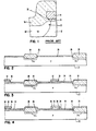
- Fig. 1 shows the resulting detailed structure of the standard process for making a polycrystalline silicon device structure.
- an insulating coating 10 of silicon dioxide is grown on the surface of the silicon body 12.
- Polycrystalline silicon conductor 14 is then blanket deposited over the layer 10.
- a masking structure, such as silicon dioxide and photoresist combination is utilized with conventional lithographic techniques to mask the polycrystalline silicon conductor in the areas where it is desired to be maintained. Other areas of the polycrystalline silicon are open for removal.
- a chemical etch is used to remove this polycrystalline silicon in the unmasked areas.
- the silicon dioxide insulator layer 10 is then removed in certain of the unmasked areas wherein it is desired to either ion implant or diffuse a region such as N+ diffused region 16.
- the N+ region 16 is then formed by diffusion or ion implantation.
- the surface is then reoxidized by conventional thermal oxidation techniques involving a wet oxygen ambient to produce oxide layer 18.
- the result of these series of process steps is shown in the prior art structure of Fig. 1 wherein it is seen that a portion of the silicon above the diffused region 16 is utilized to form the silicon dioxide 18 which results in the illustrated structure.
- a wedge region 20 of the silicon dioxide layer 18 extends underneath the polycrystalline conductor 14.
- the wedge-shaped silicon dioxide structure 20 is of poorer quality than the silicon dioxide insulator gate dielectric layer 10.
- the wing-shaped region 21 of N+ source/drain diffusions is formed by this process. It is these structures which cause yield and reduced electrical characteristics of bipolar and particularly FET integrated circuit structures.
- a process for forming a metal-oxide-silicon field effect transistor integrated circuit structure The P substrate structure of monocrystalline silicon 22 is thermally oxidized at about 1000 0 C in a suitable oxygen and/or steam atmosphere to produce a silicon dioxide layer 24.
- a chemical vapor deposition utilizing an ambient of nitrogen, hydrogen chloride gas, silicon hydrogen chloride (SiH 2 C1 2 ) and ammonia at between about 600 and 650°C is utilized to deposit a layer of silicon nitride (not shown) onto the silicon dioxide layer 24.
- Conventional lithography processes are used to open the silicon substrate 22 through the silicon dioxide and silicon nitride layers in the regions where it is desired to have a recessed oxide isolation structure.
- These layers of silicon dioxide and silicon nitride may be removed by conventional etching techniques such as chemical wet etch, reactive ion etching or plasma etching.
- a P+ boron diffusion or ion implantation is utilized to form the P+ regions 26 in the area where the recessed silicon dioxide isolation is desired.
- the recessed oxide isolation 28 is then formed at 900°C in an oxygen-water-nitrogen ambient.
- the silicon nitride layer is removed using, for example, a 10% hydrogen chloride wet chemical etch to produce the Fig. 2 structure.
- the thickness of the recessed oxide regions is of the order of 900 to 1200 nm.
- the described isolation may alternatively be replaced with other device isolation structures such as back biasing of PN junction, or complete dielectric isolation.
- the dielectric materials may be other materials or combinations of other materials, including silicon dioxide, glass, silicon nitride and aluminum trioxide. Further, other partial dielectric isolation techniques may be utilized to form this isolation.
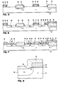
- the silicon dioxide layer 24 may either be completely removed at this point or its thickness adjusted to the desired gate dielectric silicon dioxide for the first level FET gate structure.
- This oxidation would be typically a thermal oxidation at 950°C using an ambient of oxygen, water and nitrogen.
- a coating 30 of P doped polycrystalline silicon is now deposited over the entire wafer which includes the layers 24 and 28 by using a mixture of silane and diborane in a hydrogen ambient in the temperature range of between about 500 to 1000°C.
- polycrystalline silicon can be deposited and then doped by an ion implantation process.
- the operative thickness of the polycrystalline silicon layer 30 is between about 100 to 1000 nm with typically 300 to 500 nm being preferred.
- the preferred doping level is between about 1 0 19 to 1 0 21 a t oms/cm 3 .
- a chemically vapor deposited silicon dioxide layer of between about 100 and 200 nm in thickness layer 32 is deposited over the polycrystalline silicon layer.
- a resist layer (not shown) is then deposited over the silicon dioxide layer 32.
- Standard lithographic and masking techniques are then utilized to provide a mask structure in the resist layer in areas where the polycrystalline silicon conductor structure is desired.
- the silicon doxide layer 32 is removed using the resist layer as the mask, and is removed in undesired areas by suitable etching techniques.
- the remaining silicon dioxide layer 32 is then utilized as a mask for the etching of the polycrystalline layer 30. This etching is accomplished by directional or anisotropic reactive ion etching of the polycrystalline silicon.
- the reactive ion etching or plasma etching environment for polycrystalline silicon etching is typically the conditions as follows: For example, chlorine- argon or carbon tetrachloride-argon atmosphere, RF parallel plate structure, about 10 microns pressure, 0.16 watts/ centimeter 2 power density, and 10 cc/minute flow rate.
- a critical part of the invention is to stop the reactive ion etching of the polycrystalline in the unmasked areas when a thickness of polycrystalline silicon in the order of tens of nanometers remains on the insulator coating 24.
- the preferred thickness of the remaining polycrystalline silicon in the unmasked areas is between about 20 and 100 m-n. It is preferred that the thickness be about of the order of 50 nm. This resulting structure is shown in the Fig. 3.
- the resist layer (not shown) is then removed.
- the Fig. 3 structure is then subjected to a thermal oxidation.
- the unmasked polysilicon layer 30 of the order of tens of nanometers is completely converted to a thermal silicon dioxide layer 34.
- No oxidation will occur at the FET gate dielectric edge due to the shielding of the thickness of tens of nanometers of polysilicon during this thermal oxidation.
- the quality of the gate dielectric is maintained at a high level.
- the sidewall of the polycrystalline silicon layer 30 is also converted to thermal silicon dioxide during this oxidation process. The result of this process is shown in Fig. 4.
- the layers 24 and 34 are etched anisotropically by a reactive ion etching process down to the silicon substrate. It is then possible to use a chemical dip etch to remove residual gate dielectric silicon dioxide. The horizontal located silicon dioxide is removed during this process, but the vertical or sidewall regions of the polycrystalline silicon gate remains substantially intact, as shown in Fig. 5.
- the second layer 40 of polycrystalline silicon is deposited by the identical techniques described in regard to the first layer 30.
- the doping of the polycrystalline silicon layer 40 may be simultaneous with its deposition or by means of diffusion or ion implantation following the deposition.
- a resist layer (not shown) is utilized together with conventional lithographic techniques to provide masking for the second polycrystalline silicon conductor structure.
- Reactive ion etching is now accomplished isotropically to leave the polycrystalline silicon layer in unmasked areas of the order of tens of nanometers. This again shields the polysilicon gate during subsequent oxidation and controls the second layer of polysilicon gate device sidewall consistent with the first level polysilicon gate construction.
- the resist layer is then removed.
- the second layer of polycrystalline silicon 40 is thermally oxidized to produce the silicon dioxide layer 42.
- a reactive ion etching process is used to anisotropically etch the horizontal silicon dioxide layers while allowing the vertical sidewall silicon dioxide layer to remain.
- the source and drain N+ regions 46 are diffused by conventional diffusion techniques, or a screen oxide of 20 nm or so is put down on the surface of the regions which are designated the source and drains, and an ion implantation process plus annealing is accomplished to form the regions 46. Ion implantation is considered for the purpose of this discussion to be a specie of the broad diffusion concept. Fig. 6 shows the resulting structure.
- Dry oxygen oxidation is utilized to form the reoxidation layer 48 over the source/drain diffused regions 46.
- the dry oxidation process is utilized for the same reasons described above in regard to the first polysilicon gate structure.
- the contacts to the source/drain N+ diffusions 46 are made using conventional resist, lithography and etching techniques followed by a blanket deposition of a suitable contact metallurgy and further resist, lithography and etching techniques to form the desired delineated contacts 50 to the various source and drain regions.
- a contact 52 is shown in Fig. 7 which is deposited simultaneously with the source/ drain contacts. The contact 52 contacts the second level of polycrystalline silicon.
- Fig. 8 shows a detailed view of the second polycrystalline silicon gate region of Fig. 7, similar to that shown in the prior art structure of Fig. 1. There is no silicon dioxide wedge structure, and further the wing-shaped abnormality in the diffused region at the location 54 over that of the Fig. 1 structure is much reduced.
Abstract
Description
- The invention relates to a method for making a polycrystalline silicon conductor structure in an integrated circuit.
- Polycrystalline silicon has been used for various purposes in the formation of integrated circuit structures of the field effect transistor, bipolar transistor and the like. Polycrystalline silicon has been used particularly well as conductor structures wherein it has been doped with appropriate impurities to increase its conductivity. A major use has been in the double polycrystalline silicon process for metal-oxide-silicon field effect transistor integrated circuit memories. It has been found that in using the standard pro- .cess that the product has had problems of yield and in uniformity of gate electrode characteristics. The integrated circuit devices have been studied by means of disection of the various layers of the products, and it has been found that abnormalities, particularly involving the field effect transistor gate dielectric oxide, are produced in the conventional process. These abnormalities in the field effect transistor gate silicon dioxide involve a poor quality of the silicon dioxide dielectric which can result in yield and electrical problems in the resulting integrated circuit device.
- The invention as claimed is intended to remedy these drawbacks. It solves the problem of providing a method for fabricating polycrystalline silicon layers for use in field effect transistor devices, bipolar transistor structures, and the like, which result in increased yield and improved electrical characteristics for the resulting products.
- The advantages offered by the invention are mainly that the dielectric silicon dioxide for the gate of a field effect transistor integrated device is improved. This improvement of the gate dielectric silicon dioxide does, in turn, increase the yield and improve the electrical characteristics of field effect transistor integrated circuit structures.
- This new method prevents the formation of a silicon dioxide wedge formation under the polycrystalline silicon located under the mask. This wedge of silicon dioxide which had been formed in the standard process is a poor quality silicon dioxide which has negative effects on the yields and electrical characteristics of the resulting integrated circuit structures.
- One way of carrying out the invention is described in detail below with reference to drawings which illustrate only one specific embodiment, in which:
- Fig. 1 is a drawing of a polycrystalline silicon structure of the prior art;
- Fig. 2 illustrate the process of the present invention through for producing a double polycrystalline silicon 7 field effect transistor device structure; and
- Fig. 8 is an illustration of a closeup of a portion of the Fig. 7 structure.
- Referring now more particularly to Fig. 1 which shows the resulting detailed structure of the standard process for making a polycrystalline silicon device structure. In that process, an
insulating coating 10 of silicon dioxide is grown on the surface of thesilicon body 12.Polycrystalline silicon conductor 14 is then blanket deposited over thelayer 10. A masking structure, such as silicon dioxide and photoresist combination is utilized with conventional lithographic techniques to mask the polycrystalline silicon conductor in the areas where it is desired to be maintained. Other areas of the polycrystalline silicon are open for removal. A chemical etch is used to remove this polycrystalline silicon in the unmasked areas. The silicondioxide insulator layer 10 is then removed in certain of the unmasked areas wherein it is desired to either ion implant or diffuse a region such as N+ diffusedregion 16. TheN+ region 16 is then formed by diffusion or ion implantation. The surface is then reoxidized by conventional thermal oxidation techniques involving a wet oxygen ambient to produceoxide layer 18. The result of these series of process steps is shown in the prior art structure of Fig. 1 wherein it is seen that a portion of the silicon above the diffusedregion 16 is utilized to form thesilicon dioxide 18 which results in the illustrated structure. Awedge region 20 of thesilicon dioxide layer 18 extends underneath thepolycrystalline conductor 14. The wedge-shapedsilicon dioxide structure 20 is of poorer quality than the silicon dioxide insulator gatedielectric layer 10. Also, the wing-shaped region 21 of N+ source/drain diffusions is formed by this process. It is these structures which cause yield and reduced electrical characteristics of bipolar and particularly FET integrated circuit structures. - Referring now more particularly to Figs. 2 through 7 there is shown a process for forming a metal-oxide-silicon field effect transistor integrated circuit structure. The P substrate structure of
monocrystalline silicon 22 is thermally oxidized at about 10000C in a suitable oxygen and/or steam atmosphere to produce asilicon dioxide layer 24. A chemical vapor deposition utilizing an ambient of nitrogen, hydrogen chloride gas, silicon hydrogen chloride (SiH2C12) and ammonia at between about 600 and 650°C is utilized to deposit a layer of silicon nitride (not shown) onto thesilicon dioxide layer 24. Conventional lithography processes are used to open thesilicon substrate 22 through the silicon dioxide and silicon nitride layers in the regions where it is desired to have a recessed oxide isolation structure. These layers of silicon dioxide and silicon nitride may be removed by conventional etching techniques such as chemical wet etch, reactive ion etching or plasma etching. A P+ boron diffusion or ion implantation is utilized to form theP+ regions 26 in the area where the recessed silicon dioxide isolation is desired. The recessedoxide isolation 28 is then formed at 900°C in an oxygen-water-nitrogen ambient. The silicon nitride layer is removed using, for example, a 10% hydrogen chloride wet chemical etch to produce the Fig. 2 structure. The thickness of the recessed oxide regions is of the order of 900 to 1200 nm. These recessedoxide regions 28 encircle regions of monocrystalline silicon wherein it is desired to form integrated circuit devices which are isolated from one another. - The described isolation may alternatively be replaced with other device isolation structures such as back biasing of PN junction, or complete dielectric isolation. The dielectric materials may be other materials or combinations of other materials, including silicon dioxide, glass, silicon nitride and aluminum trioxide. Further, other partial dielectric isolation techniques may be utilized to form this isolation.
- The
silicon dioxide layer 24 may either be completely removed at this point or its thickness adjusted to the desired gate dielectric silicon dioxide for the first level FET gate structure. This oxidation would be typically a thermal oxidation at 950°C using an ambient of oxygen, water and nitrogen. Acoating 30 of P doped polycrystalline silicon is now deposited over the entire wafer which includes thelayers polycrystalline silicon layer 30 is between about 100 to 1000 nm with typically 300 to 500 nm being preferred. Should the thickness be greater than about 1000 nm, planarity problems arise and make it difficult to fabricate high density integrated circuit devices. If the thickness is less than about 100 nm, the resistance of the polycrystalline silicon layer becomes significant to adversely affect the performance of the integrated circuit device. The preferred doping level is between about 10 19 to 10 21 atoms/cm 3 . - A chemically vapor deposited silicon dioxide layer of between about 100 and 200 nm in
thickness layer 32 is deposited over the polycrystalline silicon layer. A resist layer (not shown) is then deposited over thesilicon dioxide layer 32. Standard lithographic and masking techniques are then utilized to provide a mask structure in the resist layer in areas where the polycrystalline silicon conductor structure is desired. Thesilicon doxide layer 32 is removed using the resist layer as the mask, and is removed in undesired areas by suitable etching techniques. The remainingsilicon dioxide layer 32 is then utilized as a mask for the etching of thepolycrystalline layer 30. This etching is accomplished by directional or anisotropic reactive ion etching of the polycrystalline silicon. The reactive ion etching or plasma etching environment for polycrystalline silicon etching is typically the conditions as follows: For example, chlorine- argon or carbon tetrachloride-argon atmosphere, RF parallel plate structure, about 10 microns pressure, 0.16 watts/ centimeter2 power density, and 10 cc/minute flow rate. - A critical part of the invention is to stop the reactive ion etching of the polycrystalline in the unmasked areas when a thickness of polycrystalline silicon in the order of tens of nanometers remains on the
insulator coating 24. The preferred thickness of the remaining polycrystalline silicon in the unmasked areas is between about 20 and 100 m-n. It is preferred that the thickness be about of the order of 50 nm. This resulting structure is shown in the Fig. 3. The resist layer (not shown) is then removed. - The Fig. 3 structure is then subjected to a thermal oxidation. During this oxidation the
unmasked polysilicon layer 30 of the order of tens of nanometers is completely converted to a thermalsilicon dioxide layer 34. No oxidation will occur at the FET gate dielectric edge due to the shielding of the thickness of tens of nanometers of polysilicon during this thermal oxidation. Thus, the quality of the gate dielectric is maintained at a high level. The sidewall of thepolycrystalline silicon layer 30 is also converted to thermal silicon dioxide during this oxidation process. The result of this process is shown in Fig. 4. - Referring now to Fig. 5, the
layers - Next, the structure is subjected to a dry thermal oxidation by means of an oxygen ambient at a temperature of the order of 1000°C. This produces a substantially higher quality
silicon dioxide layer 38 than does the usual wet oxygen ambient, and there is no excessive silicon dioxide growth under the gate electrode. Thesecond layer 40 of polycrystalline silicon is deposited by the identical techniques described in regard to thefirst layer 30. The doping of thepolycrystalline silicon layer 40 may be simultaneous with its deposition or by means of diffusion or ion implantation following the deposition. A resist layer (not shown) is utilized together with conventional lithographic techniques to provide masking for the second polycrystalline silicon conductor structure. Reactive ion etching is now accomplished isotropically to leave the polycrystalline silicon layer in unmasked areas of the order of tens of nanometers. This again shields the polysilicon gate during subsequent oxidation and controls the second layer of polysilicon gate device sidewall consistent with the first level polysilicon gate construction. The resist layer is then removed. The second layer ofpolycrystalline silicon 40 is thermally oxidized to produce thesilicon dioxide layer 42. A reactive ion etching process is used to anisotropically etch the horizontal silicon dioxide layers while allowing the vertical sidewall silicon dioxide layer to remain. The source and drainN+ regions 46 are diffused by conventional diffusion techniques, or a screen oxide of 20 nm or so is put down on the surface of the regions which are designated the source and drains, and an ion implantation process plus annealing is accomplished to form theregions 46. Ion implantation is considered for the purpose of this discussion to be a specie of the broad diffusion concept. Fig. 6 shows the resulting structure. - Dry oxygen oxidation is utilized to form the
reoxidation layer 48 over the source/drain diffusedregions 46. The dry oxidation process is utilized for the same reasons described above in regard to the first polysilicon gate structure. The contacts to the source/drain N+ diffusions 46 are made using conventional resist, lithography and etching techniques followed by a blanket deposition of a suitable contact metallurgy and further resist, lithography and etching techniques to form the desired delineatedcontacts 50 to the various source and drain regions. Acontact 52 is shown in Fig. 7 which is deposited simultaneously with the source/ drain contacts. Thecontact 52 contacts the second level of polycrystalline silicon. - Fig. 8 shows a detailed view of the second polycrystalline silicon gate region of Fig. 7, similar to that shown in the prior art structure of Fig. 1. There is no silicon dioxide wedge structure, and further the wing-shaped abnormality in the diffused region at the
location 54 over that of the Fig. 1 structure is much reduced. - With reference to the preferred embodiments that describe the metal-oxide-silicon field effect transistor integrated circuits, it will be understood by those skilled in the art that various changes in form and detail may be made without departing from the spririt and scope of the invention. For example, the invention is equally applicable to bipolar integrated circuit and other such structures.
Claims (9)
characterized by
Applications Claiming Priority (2)
| Application Number | Priority Date | Filing Date | Title |
|---|---|---|---|
| US134039 | 1980-03-26 | ||
| US06/134,039 US4287661A (en) | 1980-03-26 | 1980-03-26 | Method for making an improved polysilicon conductor structure utilizing reactive-ion etching and thermal oxidation |
Publications (3)
| Publication Number | Publication Date |
|---|---|
| EP0036573A2 true EP0036573A2 (en) | 1981-09-30 |
| EP0036573A3 EP0036573A3 (en) | 1984-04-04 |
| EP0036573B1 EP0036573B1 (en) | 1986-10-22 |
Family
ID=22461478
Family Applications (1)
| Application Number | Title | Priority Date | Filing Date |
|---|---|---|---|
| EP81101830A Expired EP0036573B1 (en) | 1980-03-26 | 1981-03-12 | Method for making a polysilicon conductor structure |
Country Status (4)
| Country | Link |
|---|---|
| US (1) | US4287661A (en) |
| EP (1) | EP0036573B1 (en) |
| JP (1) | JPS56137678A (en) |
| DE (1) | DE3175506D1 (en) |
Cited By (3)
| Publication number | Priority date | Publication date | Assignee | Title |
|---|---|---|---|---|
| EP0081999A2 (en) * | 1981-12-16 | 1983-06-22 | Inmos Corporation | A method of fabricating a MOS transistor on a substrate |
| EP0111706A1 (en) * | 1982-12-07 | 1984-06-27 | International Business Machines Corporation | Sidewall isolation for gate of field effect transistor and process for the formation thereof |
| EP0186855A2 (en) * | 1984-12-25 | 1986-07-09 | Kabushiki Kaisha Toshiba | Semiconductor read only memory device and method of manufacturing the same |
Families Citing this family (33)
| Publication number | Priority date | Publication date | Assignee | Title |
|---|---|---|---|---|
| JPS56165362A (en) * | 1980-05-26 | 1981-12-18 | Hitachi Ltd | Manufacture of solid state color image pickup element |
| US4378627A (en) * | 1980-07-08 | 1983-04-05 | International Business Machines Corporation | Self-aligned metal process for field effect transistor integrated circuits using polycrystalline silicon gate electrodes |
| US4359816A (en) * | 1980-07-08 | 1982-11-23 | International Business Machines Corporation | Self-aligned metal process for field effect transistor integrated circuits |
| JPS5735341A (en) * | 1980-08-12 | 1982-02-25 | Toshiba Corp | Method of seperating elements of semiconductor device |
| US4404579A (en) * | 1980-10-28 | 1983-09-13 | Inc. Motorola | Semiconductor device having reduced capacitance and method of fabrication thereof |
| US4622735A (en) * | 1980-12-12 | 1986-11-18 | Tokyo Shibaura Denki Kabushiki Kaisha | Method for manufacturing a semiconductor device utilizing self-aligned silicide regions |
| US4366613A (en) * | 1980-12-17 | 1983-01-04 | Ibm Corporation | Method of fabricating an MOS dynamic RAM with lightly doped drain |
| US4389768A (en) * | 1981-04-17 | 1983-06-28 | International Business Machines Corporation | Self-aligned process for fabricating gallium arsenide metal-semiconductor field effect transistors |
| US4486943A (en) * | 1981-12-16 | 1984-12-11 | Inmos Corporation | Zero drain overlap and self aligned contact method for MOS devices |
| US4397077A (en) * | 1981-12-16 | 1983-08-09 | Inmos Corporation | Method of fabricating self-aligned MOS devices and independently formed gate dielectrics and insulating layers |
| US4419809A (en) * | 1981-12-30 | 1983-12-13 | International Business Machines Corporation | Fabrication process of sub-micrometer channel length MOSFETs |
| US4888297A (en) * | 1982-09-20 | 1989-12-19 | International Business Machines Corporation | Process for making a contact structure including polysilicon and metal alloys |
| US4592128A (en) * | 1984-06-04 | 1986-06-03 | Inmos Corporation | Method for fabricating integrated circuits with polysilicon resistors |
| IT1213192B (en) * | 1984-07-19 | 1989-12-14 | Ates Componenti Elettron | PROCESS FOR THE MANUFACTURE OF ISOLATED FIELD EFFECT TRANSISTORS (IGFET) WITH HIGH SPEED OF RESPONSE IN HIGH DENSITY INTEGRATED CIRCUITS. |
| US4686000A (en) * | 1985-04-02 | 1987-08-11 | Heath Barbara A | Self-aligned contact process |
| JPS6384067A (en) * | 1986-09-27 | 1988-04-14 | Toshiba Corp | Semiconductor device and manufacture thereof |
| US5081518A (en) * | 1989-05-24 | 1992-01-14 | National Semiconductor Corporation | Use of a polysilicon layer for local interconnect in a CMOS or BICMOS technology incorporating sidewall spacers |
| US5082796A (en) * | 1990-07-24 | 1992-01-21 | National Semiconductor Corporation | Use of polysilicon layer for local interconnect in a CMOS or BiCMOS technology incorporating sidewall spacers |
| US5795830A (en) * | 1995-06-06 | 1998-08-18 | International Business Machines Corporation | Reducing pitch with continuously adjustable line and space dimensions |
| US5882993A (en) | 1996-08-19 | 1999-03-16 | Advanced Micro Devices, Inc. | Integrated circuit with differing gate oxide thickness and process for making same |
| US6531364B1 (en) * | 1998-08-05 | 2003-03-11 | Advanced Micro Devices, Inc. | Advanced fabrication technique to form ultra thin gate dielectric using a sacrificial polysilicon seed layer |
| US5998848A (en) * | 1998-09-18 | 1999-12-07 | International Business Machines Corporation | Depleted poly-silicon edged MOSFET structure and method |
| US6130167A (en) * | 1999-03-18 | 2000-10-10 | Taiwan Semiconductor Manufacturing Company | Method of preventing corrosion of a metal structure exposed in a non-fully landed via |
| KR100507344B1 (en) * | 2003-04-17 | 2005-08-08 | 삼성에스디아이 주식회사 | Thin film transistor and method of fabricating the same |
| TWI231960B (en) * | 2004-05-31 | 2005-05-01 | Mosel Vitelic Inc | Method of forming films in the trench |
| GB0516148D0 (en) * | 2005-08-05 | 2005-09-14 | Cavendish Kinetics Ltd | Method of integrating an element |
| US9810439B2 (en) | 2011-09-02 | 2017-11-07 | Nortek Air Solutions Canada, Inc. | Energy exchange system for conditioning air in an enclosed structure |
| US9772124B2 (en) | 2013-03-13 | 2017-09-26 | Nortek Air Solutions Canada, Inc. | Heat pump defrosting system and method |
| US10352628B2 (en) | 2013-03-14 | 2019-07-16 | Nortek Air Solutions Canada, Inc. | Membrane-integrated energy exchange assembly |
| US10584884B2 (en) | 2013-03-15 | 2020-03-10 | Nortek Air Solutions Canada, Inc. | Control system and method for a liquid desiccant air delivery system |
| SG10201913923WA (en) | 2015-05-15 | 2020-03-30 | Nortek Air Solutions Canada Inc | Using liquid to air membrane energy exchanger for liquid cooling |
| US11092349B2 (en) | 2015-05-15 | 2021-08-17 | Nortek Air Solutions Canada, Inc. | Systems and methods for providing cooling to a heat load |
| CA3016808C (en) | 2016-03-08 | 2024-01-23 | Nortek Air Solutions Canada, Inc. | Systems and methods for providing cooling to a heat load |
Citations (4)
| Publication number | Priority date | Publication date | Assignee | Title |
|---|---|---|---|---|
| US3943542A (en) * | 1974-11-06 | 1976-03-09 | International Business Machines, Corporation | High reliability, low leakage, self-aligned silicon gate FET and method of fabricating same |
| GB2000643A (en) * | 1977-07-01 | 1979-01-10 | English Electric Co Ltd | Semiconductor device manufacture |
| GB2004693A (en) * | 1977-09-23 | 1979-04-04 | Siemens Ag | Improvements in or relating to the production of multi-layer silicon-gate structures on semiconducting substrates |
| EP0005165A1 (en) * | 1978-05-02 | 1979-11-14 | International Business Machines Corporation | Method of manufacturing insulated conductors of polycrystalline silicon as well as correspondingly constructed semiconductor devices with field effect elements |
Family Cites Families (9)
| Publication number | Priority date | Publication date | Assignee | Title |
|---|---|---|---|---|
| NL7204741A (en) * | 1972-04-08 | 1973-10-10 | ||
| JPS4953776A (en) * | 1972-09-27 | 1974-05-24 | ||
| JPS5910073B2 (en) * | 1972-10-27 | 1984-03-06 | 株式会社日立製作所 | Method for manufacturing silicon gate MOS type semiconductor device |
| US3961999A (en) * | 1975-06-30 | 1976-06-08 | Ibm Corporation | Method for forming recessed dielectric isolation with a minimized "bird's beak" problem |
| NL7510903A (en) * | 1975-09-17 | 1977-03-21 | Philips Nv | PROCESS FOR MANUFACTURING A SEMI-GUIDE DEVICE, AND DEVICE MANUFACTURED ACCORDING TO THE PROCESS. |
| US4104086A (en) * | 1977-08-15 | 1978-08-01 | International Business Machines Corporation | Method for forming isolated regions of silicon utilizing reactive ion etching |
| US4139442A (en) * | 1977-09-13 | 1979-02-13 | International Business Machines Corporation | Reactive ion etching method for producing deep dielectric isolation in silicon |
| US4234362A (en) * | 1978-11-03 | 1980-11-18 | International Business Machines Corporation | Method for forming an insulator between layers of conductive material |
| US4211582A (en) * | 1979-06-28 | 1980-07-08 | International Business Machines Corporation | Process for making large area isolation trenches utilizing a two-step selective etching technique |
-
1980
- 1980-03-26 US US06/134,039 patent/US4287661A/en not_active Expired - Lifetime
-
1981
- 1981-01-27 JP JP975081A patent/JPS56137678A/en active Granted
- 1981-03-12 EP EP81101830A patent/EP0036573B1/en not_active Expired
- 1981-03-12 DE DE8181101830T patent/DE3175506D1/en not_active Expired
Patent Citations (4)
| Publication number | Priority date | Publication date | Assignee | Title |
|---|---|---|---|---|
| US3943542A (en) * | 1974-11-06 | 1976-03-09 | International Business Machines, Corporation | High reliability, low leakage, self-aligned silicon gate FET and method of fabricating same |
| GB2000643A (en) * | 1977-07-01 | 1979-01-10 | English Electric Co Ltd | Semiconductor device manufacture |
| GB2004693A (en) * | 1977-09-23 | 1979-04-04 | Siemens Ag | Improvements in or relating to the production of multi-layer silicon-gate structures on semiconducting substrates |
| EP0005165A1 (en) * | 1978-05-02 | 1979-11-14 | International Business Machines Corporation | Method of manufacturing insulated conductors of polycrystalline silicon as well as correspondingly constructed semiconductor devices with field effect elements |
Non-Patent Citations (2)
| Title |
|---|
| IBM TECHNICAL DISCLOSURE BULLETIN, vol. 14, no. 10, March 1972, page 3208, New York, USA R.R. GARNACHE et al.: "Fabrication of FET structure" * |
| IBM TECHNICAL DISCLOSURE BULLETIN, vol. 22, no. 8B, January 1980, pages 3693,3694, New York, USA I. ANTIPOV; "Undercut contacts for poly si base" * |
Cited By (8)
| Publication number | Priority date | Publication date | Assignee | Title |
|---|---|---|---|---|
| EP0081999A2 (en) * | 1981-12-16 | 1983-06-22 | Inmos Corporation | A method of fabricating a MOS transistor on a substrate |
| EP0081999A3 (en) * | 1981-12-16 | 1985-01-16 | Inmos Corporation | A method of fabricating a mos transistor on a substrate |
| EP0225426A2 (en) * | 1981-12-16 | 1987-06-16 | THORN EMI North America Inc. | A method of fabricating a MOS transistor on a substrate |
| EP0225426A3 (en) * | 1981-12-16 | 1987-10-28 | Inmos Corporation | A method of fabricating a mos transistor on a substrate |
| EP0111706A1 (en) * | 1982-12-07 | 1984-06-27 | International Business Machines Corporation | Sidewall isolation for gate of field effect transistor and process for the formation thereof |
| EP0186855A2 (en) * | 1984-12-25 | 1986-07-09 | Kabushiki Kaisha Toshiba | Semiconductor read only memory device and method of manufacturing the same |
| EP0186855A3 (en) * | 1984-12-25 | 1986-10-08 | Kabushiki Kaisha Toshiba | Semiconductor read only memory device and method of manufacturing the same |
| US4755864A (en) * | 1984-12-25 | 1988-07-05 | Kabushiki Kaisha Toshiba | Semiconductor read only memory device with selectively present mask layer |
Also Published As
| Publication number | Publication date |
|---|---|
| JPS56137678A (en) | 1981-10-27 |
| JPS6152594B2 (en) | 1986-11-13 |
| EP0036573A3 (en) | 1984-04-04 |
| EP0036573B1 (en) | 1986-10-22 |
| DE3175506D1 (en) | 1986-11-27 |
| US4287661A (en) | 1981-09-08 |
Similar Documents
| Publication | Publication Date | Title |
|---|---|---|
| EP0036573B1 (en) | Method for making a polysilicon conductor structure | |
| US4209349A (en) | Method for forming a narrow dimensioned mask opening on a silicon body utilizing reactive ion etching | |
| EP0083785B1 (en) | Method of forming self-aligned field effect transistors in integrated circuit structures | |
| US4359816A (en) | Self-aligned metal process for field effect transistor integrated circuits | |
| US4378627A (en) | Self-aligned metal process for field effect transistor integrated circuits using polycrystalline silicon gate electrodes | |
| EP0083088B1 (en) | Method of producing field effect transistors having very short channel length | |
| US5654237A (en) | Method of manufacturing semiconductor device | |
| EP0083783B1 (en) | Fabrication method for integrated circuit structures including field effect transistors of sub-micrometer gate length, and integrated circuit structure fabricated by this method | |
| JPS592187B2 (en) | Method of forming an insulator between conductive layers | |
| JPS6231506B2 (en) | ||
| JPS6250969B2 (en) | ||
| EP0083784B1 (en) | Procedure for manufacturing integrated circuit devices having sub-micrometer dimension elements, and resulting structure | |
| US4322883A (en) | Self-aligned metal process for integrated injection logic integrated circuits | |
| US4488162A (en) | Self-aligned metal field effect transistor integrated circuits using polycrystalline silicon gate electrodes | |
| JPH0322053B2 (en) | ||
| US4471522A (en) | Self-aligned metal process for field effect transistor integrated circuits using polycrystalline silicon gate electrodes | |
| JPS5928983B2 (en) | Method of forming buried insulation isolation region | |
| US3837071A (en) | Method of simultaneously making a sigfet and a mosfet | |
| US4513303A (en) | Self-aligned metal field effect transistor integrated circuit | |
| US4551906A (en) | Method for making self-aligned lateral bipolar transistors | |
| US4587709A (en) | Method of making short channel IGFET | |
| US5319231A (en) | Insulated gate semiconductor device having an elevated plateau like portion | |
| US4658495A (en) | Method of forming a semiconductor structure | |
| EP0066675B1 (en) | Processes for the fabrication of field effect transistors | |
| JPS58200554A (en) | Manufacture of semiconductor device |
Legal Events
| Date | Code | Title | Description |
|---|---|---|---|
| PUAI | Public reference made under article 153(3) epc to a published international application that has entered the european phase |
Free format text: ORIGINAL CODE: 0009012 |
|
| AK | Designated contracting states |
Designated state(s): DE FR GB |
|
| 17P | Request for examination filed |
Effective date: 19811020 |
|
| PUAL | Search report despatched |
Free format text: ORIGINAL CODE: 0009013 |
|
| AK | Designated contracting states |
Designated state(s): DE FR GB |
|
| GRAA | (expected) grant |
Free format text: ORIGINAL CODE: 0009210 |
|
| AK | Designated contracting states |
Kind code of ref document: B1 Designated state(s): DE FR GB |
|
| REF | Corresponds to: |
Ref document number: 3175506 Country of ref document: DE Date of ref document: 19861127 |
|
| ET | Fr: translation filed | ||
| R20 | Corrections of a patent specification |
Effective date: 19861126 |
|
| PLBE | No opposition filed within time limit |
Free format text: ORIGINAL CODE: 0009261 |
|
| STAA | Information on the status of an ep patent application or granted ep patent |
Free format text: STATUS: NO OPPOSITION FILED WITHIN TIME LIMIT |
|
| 26N | No opposition filed | ||
| PGFP | Annual fee paid to national office [announced via postgrant information from national office to epo] |
Ref country code: GB Payment date: 19910220 Year of fee payment: 11 |
|
| PGFP | Annual fee paid to national office [announced via postgrant information from national office to epo] |
Ref country code: FR Payment date: 19910225 Year of fee payment: 11 |
|
| PGFP | Annual fee paid to national office [announced via postgrant information from national office to epo] |
Ref country code: DE Payment date: 19910323 Year of fee payment: 11 |
|
| PG25 | Lapsed in a contracting state [announced via postgrant information from national office to epo] |
Ref country code: GB Effective date: 19920312 |
|
| GBPC | Gb: european patent ceased through non-payment of renewal fee | ||
| PG25 | Lapsed in a contracting state [announced via postgrant information from national office to epo] |
Ref country code: FR Effective date: 19921130 |
|
| PG25 | Lapsed in a contracting state [announced via postgrant information from national office to epo] |
Ref country code: DE Effective date: 19921201 |
|
| REG | Reference to a national code |
Ref country code: FR Ref legal event code: ST |