JP2020041935A - Toner deposition amount sensor - Google Patents
Toner deposition amount sensor Download PDFInfo
- Publication number
- JP2020041935A JP2020041935A JP2018170305A JP2018170305A JP2020041935A JP 2020041935 A JP2020041935 A JP 2020041935A JP 2018170305 A JP2018170305 A JP 2018170305A JP 2018170305 A JP2018170305 A JP 2018170305A JP 2020041935 A JP2020041935 A JP 2020041935A
- Authority
- JP
- Japan
- Prior art keywords
- light
- receiving element
- lens
- light receiving
- substrate
- Prior art date
- Legal status (The legal status is an assumption and is not a legal conclusion. Google has not performed a legal analysis and makes no representation as to the accuracy of the status listed.)
- Granted
Links
Images


Abstract
Description
本発明は、偏光フィルタを用いないトナー付着量センサに関する。 The present invention relates to a toner adhesion amount sensor that does not use a polarizing filter.
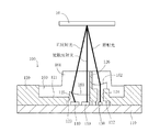
偏光フィルタを用いないトナー付着量センサとして、例えば、特許文献1または特許文献2に記載のものが知られている。図5に示すように、特許文献1に記載のトナー付着量センサ200は、基板210と、基板210上に配置されたハウジング220と、ハウジング220内の基板210上に配置された発光素子230、第1受光素子240および第2受光素子250と、を備える。
As a toner adhesion amount sensor that does not use a polarizing filter, for example, those described in Patent Literature 1 or Patent Literature 2 are known. As shown in FIG. 5, a toner
第1受光素子240と第2受光素子250は、発光素子230を挟んで互いに離れて配置されている。第1受光素子240は発光素子230の右側に配置されており、第2受光素子250は発光素子230の左側に配置されている。第1受光素子240は主に正反射光を受光し、第2受光素子250は主に拡散反射光を受光する。
The first
ハウジング220は、発光素子230の照射光が通る経路に第1絞り221を有し、正反射光が通る経路に第2絞り222を有し、拡散反射光が通る経路に第3絞り223を有する。さらに、ハウジングは、第1絞り221の上流側に、迷光の発生を抑制するための傾斜面224を有する。
The
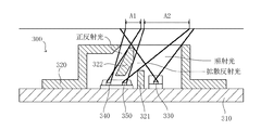
図6に示すように、特許文献2に記載のトナー付着量センサ300は、基板310と、基板310上に配置されたハウジング320と、ハウジング320内の基板310上に配置された発光素子330、第1受光素子340および第2受光素子350と、を備える。
As shown in FIG. 6, the toner
第1受光素子340と第2受光素子350は、1つのパッケージ(モールド樹脂)内に並んで配置されている。第1受光素子340は発光素子330から遠い側に配置され、第2受光素子350は発光素子330に近い側に配置されている。第1受光素子340は正反射光および拡散反射光を受光し、第2受光素子350は拡散反射光のみを受光する。
The first
ハウジング320は、第1遮光壁321と第2遮光壁322とを有する。
The
第1遮光壁321は、受光素子(第1受光素子340および第2受光素子350)と発光素子330との間に設けられている。第1遮光壁321は、発光素子330の照射光が第1受光素子340および第2受光素子350に直接入射してしまうのを防止する。
The first
第2遮光壁322は、第2受光素子350の上方に設けられている。第2遮光壁332は、測定対象物の第1反射領域A1から得られる正反射光および拡散反射光を第1受光素子340に導き、第1反射領域A1とは異なる第2反射領域A2から得られる拡散反射光のみを第2受光素子350に導くよう構成されている。すなわち、第2遮光壁322は、第1反射領域A1で発生する拡散反射光が第2受光素子350に入射してしまうのを防止する。
The second
特許文献1に記載のトナー付着量センサ200は、第1受光素子240と第2受光素子250とが発光素子230を挟んで互いに離れて配置されているため、センサ全体が大型化してしまうという問題がある。
In the toner
特許文献2に記載のトナー付着量センサ300は、第1受光素子340と第2受光素子350とが1つのパッケージ内に並んで配置されているため、特許文献1に記載のトナー付着量センサ200と比べて、センサ全体を小型化することができる。しかしながら、特許文献2に記載のトナー付着量センサ300は、ハウジング320が第1遮光壁321と第2遮光壁322とを有するため、ハウジング320の構造が複雑になり、コストアップにつながるという問題がある。
In the toner
本発明は上記事情に鑑みてなされたものであって、その課題とするところは、センサ全体の大型化および構造の複雑化を抑制可能な偏光フィルタを用いないトナー付着量センサを提供することにある。 The present invention has been made in view of the above circumstances, and an object of the present invention is to provide a toner adhesion amount sensor that does not use a polarizing filter and that can suppress an increase in the size of the entire sensor and complexity of the structure. is there.
上記課題を解決するために、本発明に係るトナー付着量センサは、
トナーの付着した測定対象物に照射光を偏光せずに照射し、前記照射光に対する前記測定対象物からの反射光を偏光せずに受光する偏光フィルタを用いないトナー付着量センサであって、
基板と、
前記基板上に配置され、前記基板上に互いに分離された第1収容空間および第2収容空間を形成するレンズホルダと、
前記第1収容空間における前記基板上に配置され、前記照射光を照射する発光素子と、
前記第2収容空間における前記基板上に配置され、前記反射光に含まれる正反射光および拡散反射光を受光する第1受光素子と、
前記第2収容空間における前記基板上に配置され、前記拡散反射光を受光する第2受光素子と、
前記レンズホルダ上に配置され、前記発光素子の上方に位置する発光レンズ部と前記第1受光素子および前記第2受光素子の上方に位置する受光レンズ部とを下面側に有するレンズと、を備え、
前記レンズホルダは、前記第1収容空間と前記第2収容空間との間に、前記レンズ内に突出する遮光壁を有し、
前記測定対象物に対する前記照射光の照射角度をθとし、前記基板の上面から前記遮光壁の上面までの高さをTとしたときに、前記遮光壁の上面を前記基板の上面に垂直投影した投影領域からTtanθ以内の領域と当該領域の内部側の領域とを含む第1領域に前記第2受光素子を配置する一方、前記第1領域の外に前記第1受光素子を配置することを特徴とする。
In order to solve the above-mentioned problem, a toner adhesion amount sensor according to the present invention includes:
Irradiation of the irradiation light to the measurement object to which the toner is adhered without polarization, a toner adhesion amount sensor without using a polarizing filter to receive the reflection light from the measurement object with respect to the irradiation light without polarization,
Board and
A lens holder disposed on the substrate and forming a first housing space and a second housing space separated from each other on the substrate;
A light-emitting element that is arranged on the substrate in the first housing space and irradiates the irradiation light;
A first light receiving element that is disposed on the substrate in the second housing space and receives regular reflection light and diffuse reflection light included in the reflected light;
A second light receiving element disposed on the substrate in the second housing space and receiving the diffuse reflected light;
A lens disposed on the lens holder and having a light-emitting lens portion positioned above the light-emitting element and a light-receiving lens portion positioned above the first light-receiving element and the second light-receiving element on a lower surface side; ,
The lens holder has a light shielding wall projecting into the lens between the first housing space and the second housing space,
When the irradiation angle of the irradiation light to the object to be measured is θ, and the height from the upper surface of the substrate to the upper surface of the light shielding wall is T, the upper surface of the light shielding wall is vertically projected on the upper surface of the substrate. The second light receiving element is arranged in a first area including an area within Ttan θ from the projection area and an area inside the area, and the first light receiving element is arranged outside the first area. And
この構成では、第2収容空間における基板上に第1受光素子および第2受光素子が配置されるので、第1受光素子と第2受光素子とを互いに近づけて配置することが可能になり、センサ全体の小型化が容易になる。 In this configuration, since the first light receiving element and the second light receiving element are arranged on the substrate in the second housing space, the first light receiving element and the second light receiving element can be arranged close to each other, and the sensor The overall size can be easily reduced.
また、この構成では、測定対象物に対する照射光の照射角度をθとし、基板の上面から遮光壁の上面までの高さをTとしたときに、遮光壁の上面を基板の上面に垂直投影した投影領域からTtanθ以内の領域を含む第1領域に第2受光素子を配置している。したがって、この構成では、レンズホルダの構造を複雑化することなく(例えば、複数の遮光壁を設けることなく)、第2受光素子に正反射光が入射するのを防ぐことができる。 Further, in this configuration, when the irradiation angle of the irradiation light to the measurement object is θ and the height from the upper surface of the substrate to the upper surface of the light shielding wall is T, the upper surface of the light shielding wall is vertically projected on the upper surface of the substrate. The second light receiving element is arranged in a first area including an area within Ttan θ from the projection area. Therefore, with this configuration, it is possible to prevent specularly reflected light from entering the second light receiving element without complicating the structure of the lens holder (for example, without providing a plurality of light shielding walls).
上記トナー付着量センサにおいて、
前記レンズは、前記正反射光および前記拡散反射光を前記測定対象物の同一の反射領域から得るとともに、前記拡散反射光を前記第2受光素子に垂直入射または前記第1受光素子側から斜入射させることが好ましい。
In the above toner adhesion amount sensor,
The lens obtains the specularly reflected light and the diffusely reflected light from the same reflection area of the object to be measured, and makes the diffusely reflected light perpendicularly incident on the second light receiving element or obliquely incident from the first light receiving element side. Preferably.
上記トナー付着量センサにおいて、
前記遮光壁は、前記レンズの上面に達しているよう構成できる。
In the above toner adhesion amount sensor,
The light shielding wall may be configured to reach an upper surface of the lens.
上記トナー付着量センサにおいて、
前記レンズホルダは、前記第1収容空間の上方に絞り部を有し、
前記絞り部は、前記照射光の照射範囲を制限するよう構成できる。
In the above toner adhesion amount sensor,
The lens holder has a diaphragm portion above the first housing space,
The aperture section may be configured to limit an irradiation range of the irradiation light.
本発明によれば、センサ全体の大型化および構造の複雑化を抑制可能な偏光フィルタを用いないトナー付着量センサを提供することができる。 According to the present invention, it is possible to provide a toner adhesion amount sensor that does not use a polarizing filter and can suppress an increase in the size of the entire sensor and a complicated structure.
以下、添付図面を参照して、本発明に係るトナー付着量センサの実施形態について説明する。 Hereinafter, an embodiment of a toner adhesion amount sensor according to the present invention will be described with reference to the accompanying drawings.
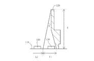
図1および図2に、本発明の一実施形態に係るトナー付着量センサ100を示す。トナー付着量センサ100は、トナーの付着した測定対象物10に照射光を偏光せずに照射し、照射光に対する測定対象物10からの反射光を偏光せずに受光する偏光フィルタを用いないセンサである。測定対象物10は、例えば、転写ベルトまたは感光体である。
1 and 2 show a toner
トナー付着量センサ100は、基板110と、レンズホルダ120と、発光素子130と、第1受光素子140と、第2受光素子150と、レンズ160とを備える。トナー付着量センサ100は、偏光フィルタを備えていない分、偏光分離方式のセンサよりもコスト面で有利である。
The toner
基板110は、例えば、矩形状のプリント配線板である。基板110の上面(実装面)には、レンズホルダ120と、発光素子130と、第1受光素子140と、第2受光素子150とが配置される。図2に示すように、発光素子130、第1受光素子140および第2受光素子150は、基板110の中央部分において、基板110の長手方向に一列に並んで配置される。
The
レンズホルダ120は、発光素子130の照射光に対して不透明な材料で構成される。レンズホルダ120は、中央部分の上面側にレンズ固定部121(凹部)を有し、中央部分の下面側に第1凹部122および第2凹部123を有する。
The
レンズ固定部121は、レンズ160を固定できるような形状に構成されている。第1凹部122は、平面視において矩形状になるように構成され、基板110上に配置された発光素子130を囲む第1収容空間を形成する。第2凹部123は、平面視において矩形状になるように構成され、基板110上に配置された第1受光素子140および第2受光素子150を囲む第2収容空間を形成する。第1収容空間と第2収容空間とは、互いに分離している。
The
また、レンズホルダ120は、第1凹部122の上方に第1開口部124を有し、第2凹部123の上方に第2開口部125を有し、第1開口部124と第2開口部125との間に遮光壁126を有する。
The
第1開口部124は、断面が楕円形状になり、かつ第1収容空間につながるよう構成されている。第1開口部124は、発光素子130の上方に位置し、発光素子130の照射光の照射範囲を制限する絞り部として機能する。これにより、第1開口部124は、測定対象物10への照射領域を狭くすることができる。
The
第2開口部125は、断面が第2凹部123とほぼ同じ大きさの矩形状になり、かつ第2収容空間につながるよう構成されている。第2開口部125は、絞り部として機能していない。第2開口部125と第2凹部123とは、1つの貫通孔で構成されていてもよい。
The
遮光壁126は、第1収容空間と第2収容空間との間において、レンズ160内に突出するよう構成されている。遮光壁126は、第2受光素子150に正反射光が入射するのを防ぐために設けられている。
The
遮光壁126は基板110の上面に対して垂直に延びており、遮光壁126の上面はレンズ160の上面に達している。これにより、遮光壁126は、レンズ160の上面で反射した発光素子130の照射光(迷光)が第1受光素子140および/または第2受光素子150に入射するのを防ぐことができる。
The
遮光壁126の第2収容空間側の側面は、第2開口部125の側面と面一になっている。また、図2に示すように、遮光壁126は平面視において矩形状になるよう構成されており、遮光壁126の幅方向(基板110の短手方向)の長さは、第1凹部122および第2凹部123の幅方向の長さと同じになっている。
The side surface of the
発光素子130は、第1収容空間における基板110上に配置され、照射光を照射する。発光素子130として、例えば、赤外線を照射する赤外発光ダイオード(赤外LED)または赤色光を照射する赤色発光ダイオード(赤色LED)を用いることができる。
The
第1受光素子140は、第2収容空間における基板110上に配置され、反射光に含まれる正反射光および拡散反射光を受光する。正反射光は、発光素子130の照射光が主に測定対象物10のトナーの付着していない領域で鏡面反射した反射光である。拡散反射光は、発光素子130の照射光が主に測定対象物10に付着しているトナーで乱反射した反射光である。
The first
第2受光素子150は、第2収容空間における基板110上であって、第1受光素子140よりも遮光壁126に近い側に配置される。第2受光素子150は、正反射光を受光することなく、拡散反射光のみを受光する。拡散反射光は、第2受光素子150に対して、垂直入射または第1受光素子140側から斜入射する。
The second
第1受光素子140および第2受光素子150としては、フォトダイオードまたはフォトトランジスタを用いることができる。本実施形態では、第1受光素子140および第2受光素子150をパッケージ(樹脂封止)されていないベアチップのまま基板110に実装しているので、第1受光素子140−第2受光素子150間の距離を短くすることができる。これにより、センサ全体の小型化が容易になる。さらに、第1受光素子140と第2受光素子150とにほぼ同量の拡散反射光を受光させることができ、両者の出力誤差を小さくすることができる。
As the first
第1受光素子140および第2受光素子150は、光電変換を行い、受光量に応じた電気信号を基板110に実装された演算回路(図示略)に出力する。演算回路は、第1受光素子140の出力と第2受光素子150の出力との差分を演算することで、正反射光の光量すなわちトナーの付着していない領域に比例した出力を得ることができる。トナーの付着量が少ない(トナーの付着していない領域が大きい)と出力値が大きくなる一方、トナーの付着量が多い(トナーの付着していない領域が小さい)と出力値が小さくなる。なお、演算回路は、トナー付着量センサ100の外部に設けられていてもよい。
The first
レンズ160は、発光素子130の照射光に対して透明な材料で構成され、レンズホルダ120の上面のレンズ固定部121に配置される。レンズ160は、上面側に凸レンズ部161を有し、下面側に発光レンズ部162および受光レンズ部163を有する。
The
凸レンズ部161は、下面側の発光レンズ部162および受光レンズ部163に対向している。凸レンズ部161の上面は平坦になっており、凸レンズ部161の幅方向の長さは遮光壁126の幅方向の長さよりも大きくなっている。
The
発光レンズ部162は、発光素子130の上方に位置して発光素子130の照射光を集光する一方、受光レンズ部163は、第1受光素子140および第2受光素子150の上方に位置して正反射光および拡散反射光を集光する。発光レンズ部162は、受光レンズ部163よりも高い位置に形成されている。
The light-emitting
発光レンズ部162および受光レンズ部163は、正反射光および拡散反射光を測定対象物10の同一の反射領域から得るとともに、第1受光素子140に対して正反射光および拡散反射光を入射させ、第2受光素子150に対して拡散反射光のみを垂直入射または第1受光素子140側から斜入射させるよう構成されている。
The light-emitting
この構成により、第1受光素子140および第2受光素子150は、同一の反射領域から拡散反射光を受光することが可能になるため、両者の出力誤差が小さくなる。その結果、トナー付着量の検出精度が向上する。
With this configuration, the first
また、この構成によれば、拡散反射光を第2受光素子150に垂直入射または第1受光素子140側から斜入射させることで、第2受光素子150を遮光壁126の近傍に配置してセンサ全体の高さを低くする(後述の第1領域L1を小さくする)ことができるとともに、第2受光素子150に正反射光が入射するのを確実に防ぐことができる。
Further, according to this configuration, the diffuse reflection light is vertically incident on the second
次に、図3を参照して、第1受光素子140および第2受光素子150の好ましい配置を説明する。
Next, a preferred arrangement of the first
発光素子130の照射光の照射角度をθとすると、正反射光の入射角度もθになる。ここで、基板110の上面から遮光壁126の上面までの高さをTとすると、遮光壁126の上面を基板110の上面に垂直投影した投影領域からTtanθ以内の第1領域L1は、正反射光が入射しない領域となる。
Assuming that the irradiation angle of the irradiation light of the
本実施形態では、第1領域L1(図3(B)のハッチング領域)に第2受光素子150を配置する一方、第1領域L1の外の第2領域L2に第1受光素子140を配置する。なお、第2受光素子150および第1受光素子140の高さは、高さTよりもはるかに小さいので無視できる。
In the present embodiment, the second
この構成により、本実施形態に係るトナー付着量センサ100は、レンズホルダ120の構造を複雑化することなく(例えば、複数の遮光壁を設けることなく)、第2受光素子150に正反射光が入射するのを防ぐことができる。
With this configuration, the toner
以上、本発明に係るトナー付着量センサの実施形態について説明したが、本発明は上記実施形態に限定されるものではない。 The embodiment of the toner adhesion amount sensor according to the present invention has been described above, but the present invention is not limited to the above embodiment.
例えば、本発明のレンズホルダは、基板110上に互いに分離された第1収容空間および第2収容空間を形成するとともに、第1収容空間と第2収容空間との間に、レンズ160内に突出する遮光壁126を有するのであれば、適宜構成を変更できる。
For example, the lens holder of the present invention forms a first housing space and a second housing space separated from each other on the
また、第2受光素子150に対して拡散反射光を第1受光素子140側から斜入射させる場合には、第2受光素子150を遮光壁126の頂部に対して遮光壁126の内部側(発光素子130側)に配置してもよい。すなわち、本発明における第1領域L1は、上記実施形態のTtanθ以内の領域と、当該領域の内部側の領域とを含む。
When the diffuse reflection light is obliquely incident on the second
図4に本発明の他の実施形態に係るトナー付着量センサの要部断面図を示す。遮光壁126の側面下部を傾斜面とすることにより、第2受光素子150を遮光壁126の内部側に配置することができる。これにより、第1受光素子140側から斜入射する拡散反射光のみを当該拡散反射光の入射を妨げることなく、第2受光素子150に受光させることができる。また、このように第2受光素子150を遮光壁126の内部側に配置して第1受光素子140と第2受光素子150とを離間させることで、トナー付着量センサ100の小型化を図りながら、仮に測定対象物10が光軸に対して傾いた場合でも、第2受光素子150に正反射光が入射するのを確実に防止することができる。
FIG. 4 is a cross-sectional view of a main part of a toner adhesion amount sensor according to another embodiment of the present invention. By making the lower part of the side surface of the
本発明の遮光壁は、上面がレンズ160の上面に達していなくてもよいし、上面がレンズ160の上面よりも上にあってもよい。
The upper surface of the light shielding wall of the present invention does not have to reach the upper surface of the
10 測定対象物
100 トナー付着量センサ
110 基板
120 レンズホルダ
121 レンズ固定部
122 第1凹部
123 第2凹部
124 第1開口部
125 第2開口部
126 遮光壁
130 発光素子
140 第1受光素子
150 第2受光素子
160 レンズ
161 凸レンズ部
162 発光レンズ部
163 受光レンズ部
Claims (4)
基板と、
前記基板上に配置され、前記基板上に互いに分離された第1収容空間および第2収容空間を形成するレンズホルダと、
前記第1収容空間における前記基板上に配置され、前記照射光を照射する発光素子と、
前記第2収容空間における前記基板上に配置され、前記反射光に含まれる正反射光および拡散反射光を受光する第1受光素子と、
前記第2収容空間における前記基板上に配置され、前記拡散反射光を受光する第2受光素子と、
前記レンズホルダ上に配置され、前記発光素子の上方に位置する発光レンズ部と前記第1受光素子および前記第2受光素子の上方に位置する受光レンズ部とを下面側に有するレンズと、を備え、
前記レンズホルダは、前記第1収容空間と前記第2収容空間との間に、前記レンズ内に突出する遮光壁を有し、
前記測定対象物に対する前記照射光の照射角度をθとし、前記基板の上面から前記遮光壁の上面までの高さをTとしたときに、前記遮光壁の上面を前記基板の上面に垂直投影した投影領域からTtanθ以内の領域と当該領域の内部側の領域とを含む第1領域に前記第2受光素子を配置する一方、前記第1領域の外に前記第1受光素子を配置する
ことを特徴とするトナー付着量センサ。 Irradiation of the irradiation light to the measurement object to which the toner is adhered without polarization, a toner adhesion amount sensor without using a polarizing filter to receive the reflection light from the measurement object with respect to the irradiation light without polarization,
Board and
A lens holder disposed on the substrate and forming a first housing space and a second housing space separated from each other on the substrate;
A light-emitting element that is arranged on the substrate in the first housing space and irradiates the irradiation light;
A first light receiving element that is disposed on the substrate in the second housing space and receives regular reflection light and diffuse reflection light included in the reflected light;
A second light receiving element disposed on the substrate in the second housing space and receiving the diffuse reflected light;
A lens disposed on the lens holder and having a light-emitting lens portion positioned above the light-emitting element and a light-receiving lens portion positioned above the first light-receiving element and the second light-receiving element on a lower surface side; ,
The lens holder has a light shielding wall projecting into the lens between the first housing space and the second housing space,
When the irradiation angle of the irradiation light to the object to be measured is θ, and the height from the upper surface of the substrate to the upper surface of the light shielding wall is T, the upper surface of the light shielding wall is vertically projected on the upper surface of the substrate. The second light receiving element is arranged in a first area including an area within Ttan θ from the projection area and an area inside the area, and the first light receiving element is arranged outside the first area. Toner amount sensor.
ことを特徴とする請求項1に記載のトナー付着量センサ。 The lens obtains the specularly reflected light and the diffusely reflected light from the same reflection area of the object to be measured, and makes the diffusely reflected light perpendicularly incident on the second light receiving element or obliquely incident from the first light receiving element side. The toner adhesion amount sensor according to claim 1, wherein
ことを特徴とする請求項1または2に記載のトナー付着量センサ。 3. The toner adhesion amount sensor according to claim 1, wherein the light shielding wall reaches an upper surface of the lens.
前記絞り部は、前記照射光の照射範囲を制限する
ことを特徴とする請求項1〜3のいずれか一項に記載のトナー付着量センサ。 The lens holder has a diaphragm portion above the first housing space,
4. The toner adhesion amount sensor according to claim 1, wherein the aperture unit limits an irradiation range of the irradiation light. 5.
Priority Applications (1)
| Application Number | Priority Date | Filing Date | Title |
|---|---|---|---|
| JP2018170305A JP7093275B2 (en) | 2018-09-12 | 2018-09-12 | Toner adhesion sensor |
Applications Claiming Priority (1)
| Application Number | Priority Date | Filing Date | Title |
|---|---|---|---|
| JP2018170305A JP7093275B2 (en) | 2018-09-12 | 2018-09-12 | Toner adhesion sensor |
Publications (2)
| Publication Number | Publication Date |
|---|---|
| JP2020041935A true JP2020041935A (en) | 2020-03-19 |
| JP7093275B2 JP7093275B2 (en) | 2022-06-29 |
Family
ID=69799390
Family Applications (1)
| Application Number | Title | Priority Date | Filing Date |
|---|---|---|---|
| JP2018170305A Active JP7093275B2 (en) | 2018-09-12 | 2018-09-12 | Toner adhesion sensor |
Country Status (1)
| Country | Link |
|---|---|
| JP (1) | JP7093275B2 (en) |
Cited By (2)
| Publication number | Priority date | Publication date | Assignee | Title |
|---|---|---|---|---|
| JP2021135152A (en) * | 2020-02-27 | 2021-09-13 | ニチコン株式会社 | Basis weight measuring device and method for measuring basis weight |
| JP2021173668A (en) * | 2020-04-27 | 2021-11-01 | ニチコン株式会社 | Reflection type sensor |
Citations (7)
| Publication number | Priority date | Publication date | Assignee | Title |
|---|---|---|---|---|
| JPH08233653A (en) * | 1994-11-25 | 1996-09-13 | Xerox Corp | Densitiometer for measuring diffusion reflectivity |
| JP2005091252A (en) * | 2003-09-19 | 2005-04-07 | Ricoh Co Ltd | Optical sensor |
| JP2006208266A (en) * | 2005-01-31 | 2006-08-10 | Nichicon Corp | Toner adhesion quantity measuring apparatus |
| US7544923B1 (en) * | 2008-01-25 | 2009-06-09 | Xerox Corporation | LED signature elimination in specular-mode LED illumination having a light diffuser between an illuminator array and an image bearing surface |
| JP2013195066A (en) * | 2012-03-15 | 2013-09-30 | Omron Corp | Toner density sensor and image forming device |
| JP2017116636A (en) * | 2015-12-22 | 2017-06-29 | ニチコン株式会社 | Toner adhesion amount sensor |
| JP2018137340A (en) * | 2017-02-22 | 2018-08-30 | ニチコン株式会社 | Toner adhesion amount sensor and manufacturing method thereof |
-
2018
- 2018-09-12 JP JP2018170305A patent/JP7093275B2/en active Active
Patent Citations (7)
| Publication number | Priority date | Publication date | Assignee | Title |
|---|---|---|---|---|
| JPH08233653A (en) * | 1994-11-25 | 1996-09-13 | Xerox Corp | Densitiometer for measuring diffusion reflectivity |
| JP2005091252A (en) * | 2003-09-19 | 2005-04-07 | Ricoh Co Ltd | Optical sensor |
| JP2006208266A (en) * | 2005-01-31 | 2006-08-10 | Nichicon Corp | Toner adhesion quantity measuring apparatus |
| US7544923B1 (en) * | 2008-01-25 | 2009-06-09 | Xerox Corporation | LED signature elimination in specular-mode LED illumination having a light diffuser between an illuminator array and an image bearing surface |
| JP2013195066A (en) * | 2012-03-15 | 2013-09-30 | Omron Corp | Toner density sensor and image forming device |
| JP2017116636A (en) * | 2015-12-22 | 2017-06-29 | ニチコン株式会社 | Toner adhesion amount sensor |
| JP2018137340A (en) * | 2017-02-22 | 2018-08-30 | ニチコン株式会社 | Toner adhesion amount sensor and manufacturing method thereof |
Cited By (2)
| Publication number | Priority date | Publication date | Assignee | Title |
|---|---|---|---|---|
| JP2021135152A (en) * | 2020-02-27 | 2021-09-13 | ニチコン株式会社 | Basis weight measuring device and method for measuring basis weight |
| JP2021173668A (en) * | 2020-04-27 | 2021-11-01 | ニチコン株式会社 | Reflection type sensor |
Also Published As
| Publication number | Publication date |
|---|---|
| JP7093275B2 (en) | 2022-06-29 |
Similar Documents
| Publication | Publication Date | Title |
|---|---|---|
| US9134224B2 (en) | Gas component detection device | |
| US7417716B2 (en) | Multiple ranging apparatus | |
| TWI451072B (en) | Spectral module | |
| JP2008051764A (en) | Range finding sensor, and electronic device having sensor mounted | |
| KR101640989B1 (en) | Limited area reflective optical sensor and electronic device | |
| JP7093275B2 (en) | Toner adhesion sensor | |
| JP6552052B2 (en) | Toner adhesion amount sensor | |
| JP2000089394A (en) | Original detector and detector | |
| JP4616676B2 (en) | Color toner adhesion measuring device | |
| JP4466083B2 (en) | Ranging light source and ranging device | |
| WO2012140482A1 (en) | Gas component detection device | |
| JP2019139830A (en) | Limited reflection type sensor | |
| JP2007059657A (en) | Photo interrupter | |
| JP2003332614A (en) | Optical coupling device and information apparatus using the same | |
| JP6718832B2 (en) | Radiation detector and radiation detection device | |
| JP5278276B2 (en) | Ranging light source and ranging device using the same | |
| JP2002350554A (en) | Transmission type photoelectric sensor | |
| JP2007327822A (en) | Optical encoder and electronic device using the same | |
| JP2003195428A (en) | Original existence detection sensor, original size detection sensor and image reader | |
| JP6817479B1 (en) | Reflective sensor | |
| JP2018115955A (en) | Radiation detector and radiation detection device | |
| JP2006147944A (en) | Photo interrupter | |
| JP2023076120A (en) | photoelectric sensor | |
| JPH0972727A (en) | Optical sensor | |
| JP2000266542A (en) | Optical inclination sensor |
Legal Events
| Date | Code | Title | Description |
|---|---|---|---|
| A621 | Written request for application examination |
Free format text: JAPANESE INTERMEDIATE CODE: A621 Effective date: 20210312 |
|
| A977 | Report on retrieval |
Free format text: JAPANESE INTERMEDIATE CODE: A971007 Effective date: 20211217 |
|
| A131 | Notification of reasons for refusal |
Free format text: JAPANESE INTERMEDIATE CODE: A131 Effective date: 20220105 |
|
| A521 | Request for written amendment filed |
Free format text: JAPANESE INTERMEDIATE CODE: A523 Effective date: 20220224 |
|
| TRDD | Decision of grant or rejection written | ||
| A01 | Written decision to grant a patent or to grant a registration (utility model) |
Free format text: JAPANESE INTERMEDIATE CODE: A01 Effective date: 20220615 |
|
| A61 | First payment of annual fees (during grant procedure) |
Free format text: JAPANESE INTERMEDIATE CODE: A61 Effective date: 20220617 |
|
| R150 | Certificate of patent or registration of utility model |
Ref document number: 7093275 Country of ref document: JP Free format text: JAPANESE INTERMEDIATE CODE: R150 |