JP2019061973A - Light-emitting device - Google Patents
Light-emitting device Download PDFInfo
- Publication number
- JP2019061973A JP2019061973A JP2019012989A JP2019012989A JP2019061973A JP 2019061973 A JP2019061973 A JP 2019061973A JP 2019012989 A JP2019012989 A JP 2019012989A JP 2019012989 A JP2019012989 A JP 2019012989A JP 2019061973 A JP2019061973 A JP 2019061973A
- Authority
- JP
- Japan
- Prior art keywords
- light emitting
- emitting element
- light
- layer
- emission
- Prior art date
- Legal status (The legal status is an assumption and is not a legal conclusion. Google has not performed a legal analysis and makes no representation as to the accuracy of the status listed.)
- Withdrawn
Links
- 238000000295 emission spectrum Methods 0.000 claims abstract description 88
- 239000000758 substrate Substances 0.000 abstract description 35
- 238000001228 spectrum Methods 0.000 abstract description 25
- 230000008859 change Effects 0.000 abstract description 5
- 239000010410 layer Substances 0.000 description 224
- 239000010408 film Substances 0.000 description 55
- 238000002347 injection Methods 0.000 description 42
- 239000007924 injection Substances 0.000 description 42
- 239000000463 material Substances 0.000 description 41
- 150000002894 organic compounds Chemical class 0.000 description 27
- 230000000295 complement effect Effects 0.000 description 20
- 229910052744 lithium Inorganic materials 0.000 description 20
- IBHBKWKFFTZAHE-UHFFFAOYSA-N n-[4-[4-(n-naphthalen-1-ylanilino)phenyl]phenyl]-n-phenylnaphthalen-1-amine Chemical group C1=CC=CC=C1N(C=1C2=CC=CC=C2C=CC=1)C1=CC=C(C=2C=CC(=CC=2)N(C=2C=CC=CC=2)C=2C3=CC=CC=C3C=CC=2)C=C1 IBHBKWKFFTZAHE-UHFFFAOYSA-N 0.000 description 20
- 238000000034 method Methods 0.000 description 18
- WHXSMMKQMYFTQS-UHFFFAOYSA-N Lithium Chemical compound [Li] WHXSMMKQMYFTQS-UHFFFAOYSA-N 0.000 description 17
- 239000003086 colorant Substances 0.000 description 17
- -1 Aromatic amine compounds Chemical class 0.000 description 16
- 230000015572 biosynthetic process Effects 0.000 description 16
- 238000005755 formation reaction Methods 0.000 description 16
- 238000001704 evaporation Methods 0.000 description 15
- 230000008020 evaporation Effects 0.000 description 13
- 238000007738 vacuum evaporation Methods 0.000 description 12
- 229910052782 aluminium Inorganic materials 0.000 description 11
- 238000010549 co-Evaporation Methods 0.000 description 11
- 230000001747 exhibiting effect Effects 0.000 description 11
- 239000000126 substance Substances 0.000 description 11
- NRTOMJZYCJJWKI-UHFFFAOYSA-N Titanium nitride Chemical compound [Ti]#N NRTOMJZYCJJWKI-UHFFFAOYSA-N 0.000 description 10
- 239000011701 zinc Substances 0.000 description 10
- XLOMVQKBTHCTTD-UHFFFAOYSA-N Zinc monoxide Chemical compound [Zn]=O XLOMVQKBTHCTTD-UHFFFAOYSA-N 0.000 description 9
- CUJRVFIICFDLGR-UHFFFAOYSA-N acetylacetonate Chemical compound CC(=O)[CH-]C(C)=O CUJRVFIICFDLGR-UHFFFAOYSA-N 0.000 description 9
- XAGFODPZIPBFFR-UHFFFAOYSA-N aluminium Chemical compound [Al] XAGFODPZIPBFFR-UHFFFAOYSA-N 0.000 description 9
- 230000005525 hole transport Effects 0.000 description 9
- 150000001875 compounds Chemical class 0.000 description 8
- 239000011521 glass Substances 0.000 description 8
- 239000012212 insulator Substances 0.000 description 8
- 239000010409 thin film Substances 0.000 description 8
- 230000005281 excited state Effects 0.000 description 7
- 238000004519 manufacturing process Methods 0.000 description 7
- ZNJRONVKWRHYBF-VOTSOKGWSA-N 4-(dicyanomethylene)-2-methyl-6-julolidyl-9-enyl-4h-pyran Chemical compound O1C(C)=CC(=C(C#N)C#N)C=C1\C=C\C1=CC(CCCN2CCC3)=C2C3=C1 ZNJRONVKWRHYBF-VOTSOKGWSA-N 0.000 description 6
- 229910052783 alkali metal Inorganic materials 0.000 description 6
- 150000001340 alkali metals Chemical class 0.000 description 6
- 230000008901 benefit Effects 0.000 description 6
- 125000002080 perylenyl group Chemical group C1(=CC=C2C=CC=C3C4=CC=CC5=CC=CC(C1=C23)=C45)* 0.000 description 6
- 238000001771 vacuum deposition Methods 0.000 description 6
- POXIZPBFFUKMEQ-UHFFFAOYSA-N 2-cyanoethenylideneazanide Chemical group [N-]=C=[C+]C#N POXIZPBFFUKMEQ-UHFFFAOYSA-N 0.000 description 5
- VFUDMQLBKNMONU-UHFFFAOYSA-N 9-[4-(4-carbazol-9-ylphenyl)phenyl]carbazole Chemical group C12=CC=CC=C2C2=CC=CC=C2N1C1=CC=C(C=2C=CC(=CC=2)N2C3=CC=CC=C3C3=CC=CC=C32)C=C1 VFUDMQLBKNMONU-UHFFFAOYSA-N 0.000 description 5
- VYPSYNLAJGMNEJ-UHFFFAOYSA-N Silicium dioxide Chemical compound O=[Si]=O VYPSYNLAJGMNEJ-UHFFFAOYSA-N 0.000 description 5
- HCHKCACWOHOZIP-UHFFFAOYSA-N Zinc Chemical compound [Zn] HCHKCACWOHOZIP-UHFFFAOYSA-N 0.000 description 5
- 229910052784 alkaline earth metal Inorganic materials 0.000 description 5
- 150000001342 alkaline earth metals Chemical class 0.000 description 5
- AMGQUBHHOARCQH-UHFFFAOYSA-N indium;oxotin Chemical compound [In].[Sn]=O AMGQUBHHOARCQH-UHFFFAOYSA-N 0.000 description 5
- 150000002484 inorganic compounds Chemical class 0.000 description 5
- 238000003475 lamination Methods 0.000 description 5
- 229910052751 metal Inorganic materials 0.000 description 5
- 239000002184 metal Substances 0.000 description 5
- CSHWQDPOILHKBI-UHFFFAOYSA-N peryrene Natural products C1=CC(C2=CC=CC=3C2=C2C=CC=3)=C3C2=CC=CC3=C1 CSHWQDPOILHKBI-UHFFFAOYSA-N 0.000 description 5
- 238000007789 sealing Methods 0.000 description 5
- 239000003566 sealing material Substances 0.000 description 5
- 229910052725 zinc Inorganic materials 0.000 description 5
- 239000007983 Tris buffer Substances 0.000 description 4
- 239000000956 alloy Substances 0.000 description 4
- 229910045601 alloy Inorganic materials 0.000 description 4
- UFVXQDWNSAGPHN-UHFFFAOYSA-K bis[(2-methylquinolin-8-yl)oxy]-(4-phenylphenoxy)alumane Chemical compound [Al+3].C1=CC=C([O-])C2=NC(C)=CC=C21.C1=CC=C([O-])C2=NC(C)=CC=C21.C1=CC([O-])=CC=C1C1=CC=CC=C1 UFVXQDWNSAGPHN-UHFFFAOYSA-K 0.000 description 4
- NNBFNNNWANBMTI-UHFFFAOYSA-M brilliant green Chemical compound OS([O-])(=O)=O.C1=CC(N(CC)CC)=CC=C1C(C=1C=CC=CC=1)=C1C=CC(=[N+](CC)CC)C=C1 NNBFNNNWANBMTI-UHFFFAOYSA-M 0.000 description 4
- 239000004020 conductor Substances 0.000 description 4
- 230000001419 dependent effect Effects 0.000 description 4
- ZUOUZKKEUPVFJK-UHFFFAOYSA-N diphenyl Chemical compound C1=CC=CC=C1C1=CC=CC=C1 ZUOUZKKEUPVFJK-UHFFFAOYSA-N 0.000 description 4
- 229910010272 inorganic material Inorganic materials 0.000 description 4
- 229920000642 polymer Polymers 0.000 description 4
- 229910052814 silicon oxide Inorganic materials 0.000 description 4
- STCOOQWBFONSKY-UHFFFAOYSA-N tributyl phosphate Chemical compound CCCCOP(=O)(OCCCC)OCCCC STCOOQWBFONSKY-UHFFFAOYSA-N 0.000 description 4
- 239000011787 zinc oxide Substances 0.000 description 4
- SPDPTFAJSFKAMT-UHFFFAOYSA-N 1-n-[4-[4-(n-[4-(3-methyl-n-(3-methylphenyl)anilino)phenyl]anilino)phenyl]phenyl]-4-n,4-n-bis(3-methylphenyl)-1-n-phenylbenzene-1,4-diamine Chemical compound CC1=CC=CC(N(C=2C=CC(=CC=2)N(C=2C=CC=CC=2)C=2C=CC(=CC=2)C=2C=CC(=CC=2)N(C=2C=CC=CC=2)C=2C=CC(=CC=2)N(C=2C=C(C)C=CC=2)C=2C=C(C)C=CC=2)C=2C=C(C)C=CC=2)=C1 SPDPTFAJSFKAMT-UHFFFAOYSA-N 0.000 description 3
- DHDHJYNTEFLIHY-UHFFFAOYSA-N 4,7-diphenyl-1,10-phenanthroline Chemical compound C1=CC=CC=C1C1=CC=NC2=C1C=CC1=C(C=3C=CC=CC=3)C=CN=C21 DHDHJYNTEFLIHY-UHFFFAOYSA-N 0.000 description 3
- UHOVQNZJYSORNB-UHFFFAOYSA-N Benzene Chemical compound C1=CC=CC=C1 UHOVQNZJYSORNB-UHFFFAOYSA-N 0.000 description 3
- 229910004261 CaF 2 Inorganic materials 0.000 description 3
- 230000005284 excitation Effects 0.000 description 3
- 238000010030 laminating Methods 0.000 description 3
- 238000001748 luminescence spectrum Methods 0.000 description 3
- 229910052757 nitrogen Inorganic materials 0.000 description 3
- YRZZLAGRKZIJJI-UHFFFAOYSA-N oxyvanadium phthalocyanine Chemical compound [V+2]=O.C12=CC=CC=C2C(N=C2[N-]C(C3=CC=CC=C32)=N2)=NC1=NC([C]1C=CC=CC1=1)=NC=1N=C1[C]3C=CC=CC3=C2[N-]1 YRZZLAGRKZIJJI-UHFFFAOYSA-N 0.000 description 3
- UOCMXZLNHQBBOS-UHFFFAOYSA-N 2-(1,3-benzoxazol-2-yl)phenol zinc Chemical compound [Zn].Oc1ccccc1-c1nc2ccccc2o1.Oc1ccccc1-c1nc2ccccc2o1 UOCMXZLNHQBBOS-UHFFFAOYSA-N 0.000 description 2
- FQJQNLKWTRGIEB-UHFFFAOYSA-N 2-(4-tert-butylphenyl)-5-[3-[5-(4-tert-butylphenyl)-1,3,4-oxadiazol-2-yl]phenyl]-1,3,4-oxadiazole Chemical compound C1=CC(C(C)(C)C)=CC=C1C1=NN=C(C=2C=C(C=CC=2)C=2OC(=NN=2)C=2C=CC(=CC=2)C(C)(C)C)O1 FQJQNLKWTRGIEB-UHFFFAOYSA-N 0.000 description 2
- YLYPIBBGWLKELC-RMKNXTFCSA-N 2-[2-[(e)-2-[4-(dimethylamino)phenyl]ethenyl]-6-methylpyran-4-ylidene]propanedinitrile Chemical compound C1=CC(N(C)C)=CC=C1\C=C\C1=CC(=C(C#N)C#N)C=C(C)O1 YLYPIBBGWLKELC-RMKNXTFCSA-N 0.000 description 2
- ZNJRONVKWRHYBF-UHFFFAOYSA-N 2-[2-[2-(1-azatricyclo[7.3.1.05,13]trideca-5,7,9(13)-trien-7-yl)ethenyl]-6-methylpyran-4-ylidene]propanedinitrile Chemical compound O1C(C)=CC(=C(C#N)C#N)C=C1C=CC1=CC(CCCN2CCC3)=C2C3=C1 ZNJRONVKWRHYBF-UHFFFAOYSA-N 0.000 description 2
- GEQBRULPNIVQPP-UHFFFAOYSA-N 2-[3,5-bis(1-phenylbenzimidazol-2-yl)phenyl]-1-phenylbenzimidazole Chemical compound C1=CC=CC=C1N1C2=CC=CC=C2N=C1C1=CC(C=2N(C3=CC=CC=C3N=2)C=2C=CC=CC=2)=CC(C=2N(C3=CC=CC=C3N=2)C=2C=CC=CC=2)=C1 GEQBRULPNIVQPP-UHFFFAOYSA-N 0.000 description 2
- 125000000175 2-thienyl group Chemical group S1C([*])=C([H])C([H])=C1[H] 0.000 description 2
- ZVFQEOPUXVPSLB-UHFFFAOYSA-N 3-(4-tert-butylphenyl)-4-phenyl-5-(4-phenylphenyl)-1,2,4-triazole Chemical compound C1=CC(C(C)(C)C)=CC=C1C(N1C=2C=CC=CC=2)=NN=C1C1=CC=C(C=2C=CC=CC=2)C=C1 ZVFQEOPUXVPSLB-UHFFFAOYSA-N 0.000 description 2
- XKRFYHLGVUSROY-UHFFFAOYSA-N Argon Chemical compound [Ar] XKRFYHLGVUSROY-UHFFFAOYSA-N 0.000 description 2
- IJGRMHOSHXDMSA-UHFFFAOYSA-N Atomic nitrogen Chemical compound N#N IJGRMHOSHXDMSA-UHFFFAOYSA-N 0.000 description 2
- 229910018068 Li 2 O Inorganic materials 0.000 description 2
- 229920001609 Poly(3,4-ethylenedioxythiophene) Polymers 0.000 description 2
- NIXOWILDQLNWCW-UHFFFAOYSA-N acrylic acid group Chemical group C(C=C)(=O)O NIXOWILDQLNWCW-UHFFFAOYSA-N 0.000 description 2
- 235000010290 biphenyl Nutrition 0.000 description 2
- 239000004305 biphenyl Substances 0.000 description 2
- 229910052792 caesium Inorganic materials 0.000 description 2
- 229910052804 chromium Inorganic materials 0.000 description 2
- 239000011651 chromium Substances 0.000 description 2
- ZYGHJZDHTFUPRJ-UHFFFAOYSA-N coumarin Chemical compound C1=CC=C2OC(=O)C=CC2=C1 ZYGHJZDHTFUPRJ-UHFFFAOYSA-N 0.000 description 2
- 230000007423 decrease Effects 0.000 description 2
- 238000000151 deposition Methods 0.000 description 2
- 125000002147 dimethylamino group Chemical group [H]C([H])([H])N(*)C([H])([H])[H] 0.000 description 2
- 238000010438 heat treatment Methods 0.000 description 2
- 238000005286 illumination Methods 0.000 description 2
- RHZWSUVWRRXEJF-UHFFFAOYSA-N indium tin Chemical compound [In].[Sn] RHZWSUVWRRXEJF-UHFFFAOYSA-N 0.000 description 2
- 229910052749 magnesium Inorganic materials 0.000 description 2
- IEQIEDJGQAUEQZ-UHFFFAOYSA-N phthalocyanine Chemical class N1C(N=C2C3=CC=CC=C3C(N=C3C4=CC=CC=C4C(=N4)N3)=N2)=C(C=CC=C2)C2=C1N=C1C2=CC=CC=C2C4=N1 IEQIEDJGQAUEQZ-UHFFFAOYSA-N 0.000 description 2
- 229920003023 plastic Polymers 0.000 description 2
- 239000004033 plastic Substances 0.000 description 2
- 229920002620 polyvinyl fluoride Polymers 0.000 description 2
- 229910052761 rare earth metal Inorganic materials 0.000 description 2
- 150000002910 rare earth metals Chemical class 0.000 description 2
- 230000006798 recombination Effects 0.000 description 2
- 238000005215 recombination Methods 0.000 description 2
- 238000012827 research and development Methods 0.000 description 2
- 239000000565 sealant Substances 0.000 description 2
- 239000002356 single layer Substances 0.000 description 2
- 125000005504 styryl group Chemical group 0.000 description 2
- 239000010936 titanium Substances 0.000 description 2
- 229910052719 titanium Inorganic materials 0.000 description 2
- 229910052721 tungsten Inorganic materials 0.000 description 2
- YVTHLONGBIQYBO-UHFFFAOYSA-N zinc indium(3+) oxygen(2-) Chemical compound [O--].[Zn++].[In+3] YVTHLONGBIQYBO-UHFFFAOYSA-N 0.000 description 2
- POILWHVDKZOXJZ-ARJAWSKDSA-M (z)-4-oxopent-2-en-2-olate Chemical compound C\C([O-])=C\C(C)=O POILWHVDKZOXJZ-ARJAWSKDSA-M 0.000 description 1
- RTSZQXSYCGBHMO-UHFFFAOYSA-N 1,2,4-trichloro-3-prop-1-ynoxybenzene Chemical compound CC#COC1=C(Cl)C=CC(Cl)=C1Cl RTSZQXSYCGBHMO-UHFFFAOYSA-N 0.000 description 1
- UHXOHPVVEHBKKT-UHFFFAOYSA-N 1-(2,2-diphenylethenyl)-4-[4-(2,2-diphenylethenyl)phenyl]benzene Chemical compound C=1C=C(C=2C=CC(C=C(C=3C=CC=CC=3)C=3C=CC=CC=3)=CC=2)C=CC=1C=C(C=1C=CC=CC=1)C1=CC=CC=C1 UHXOHPVVEHBKKT-UHFFFAOYSA-N 0.000 description 1
- IJVBYWCDGKXHKK-UHFFFAOYSA-N 1-n,1-n,2-n,2-n-tetraphenylbenzene-1,2-diamine Chemical compound C1=CC=CC=C1N(C=1C(=CC=CC=1)N(C=1C=CC=CC=1)C=1C=CC=CC=1)C1=CC=CC=C1 IJVBYWCDGKXHKK-UHFFFAOYSA-N 0.000 description 1
- IYZMXHQDXZKNCY-UHFFFAOYSA-N 1-n,1-n-diphenyl-4-n,4-n-bis[4-(n-phenylanilino)phenyl]benzene-1,4-diamine Chemical compound C1=CC=CC=C1N(C=1C=CC(=CC=1)N(C=1C=CC(=CC=1)N(C=1C=CC=CC=1)C=1C=CC=CC=1)C=1C=CC(=CC=1)N(C=1C=CC=CC=1)C=1C=CC=CC=1)C1=CC=CC=C1 IYZMXHQDXZKNCY-UHFFFAOYSA-N 0.000 description 1
- HYZJCKYKOHLVJF-UHFFFAOYSA-N 1H-benzimidazole Chemical compound C1=CC=C2NC=NC2=C1 HYZJCKYKOHLVJF-UHFFFAOYSA-N 0.000 description 1
- 125000004215 2,4-difluorophenyl group Chemical group [H]C1=C([H])C(*)=C(F)C([H])=C1F 0.000 description 1
- BFTIPCRZWILUIY-UHFFFAOYSA-N 2,5,8,11-tetratert-butylperylene Chemical group CC(C)(C)C1=CC(C2=CC(C(C)(C)C)=CC=3C2=C2C=C(C=3)C(C)(C)C)=C3C2=CC(C(C)(C)C)=CC3=C1 BFTIPCRZWILUIY-UHFFFAOYSA-N 0.000 description 1
- STTGYIUESPWXOW-UHFFFAOYSA-N 2,9-dimethyl-4,7-diphenyl-1,10-phenanthroline Chemical compound C=12C=CC3=C(C=4C=CC=CC=4)C=C(C)N=C3C2=NC(C)=CC=1C1=CC=CC=C1 STTGYIUESPWXOW-UHFFFAOYSA-N 0.000 description 1
- IXHWGNYCZPISET-UHFFFAOYSA-N 2-[4-(dicyanomethylidene)-2,3,5,6-tetrafluorocyclohexa-2,5-dien-1-ylidene]propanedinitrile Chemical compound FC1=C(F)C(=C(C#N)C#N)C(F)=C(F)C1=C(C#N)C#N IXHWGNYCZPISET-UHFFFAOYSA-N 0.000 description 1
- UUNIOFWUJYBVGQ-UHFFFAOYSA-N 2-amino-4-(3,4-dimethoxyphenyl)-10-fluoro-4,5,6,7-tetrahydrobenzo[1,2]cyclohepta[6,7-d]pyran-3-carbonitrile Chemical compound C1=C(OC)C(OC)=CC=C1C1C(C#N)=C(N)OC2=C1CCCC1=CC=C(F)C=C12 UUNIOFWUJYBVGQ-UHFFFAOYSA-N 0.000 description 1
- HONWGFNQCPRRFM-UHFFFAOYSA-N 2-n-(3-methylphenyl)-1-n,1-n,2-n-triphenylbenzene-1,2-diamine Chemical compound CC1=CC=CC(N(C=2C=CC=CC=2)C=2C(=CC=CC=2)N(C=2C=CC=CC=2)C=2C=CC=CC=2)=C1 HONWGFNQCPRRFM-UHFFFAOYSA-N 0.000 description 1
- NSMJMUQZRGZMQC-UHFFFAOYSA-N 2-naphthalen-1-yl-1H-imidazo[4,5-f][1,10]phenanthroline Chemical compound C12=CC=CN=C2C2=NC=CC=C2C2=C1NC(C=1C3=CC=CC=C3C=CC=1)=N2 NSMJMUQZRGZMQC-UHFFFAOYSA-N 0.000 description 1
- AWXGSYPUMWKTBR-UHFFFAOYSA-N 4-carbazol-9-yl-n,n-bis(4-carbazol-9-ylphenyl)aniline Chemical compound C12=CC=CC=C2C2=CC=CC=C2N1C1=CC=C(N(C=2C=CC(=CC=2)N2C3=CC=CC=C3C3=CC=CC=C32)C=2C=CC(=CC=2)N2C3=CC=CC=C3C3=CC=CC=C32)C=C1 AWXGSYPUMWKTBR-UHFFFAOYSA-N 0.000 description 1
- 125000004860 4-ethylphenyl group Chemical group [H]C1=C([H])C(=C([H])C([H])=C1*)C([H])([H])C([H])([H])[H] 0.000 description 1
- VIZUPBYFLORCRA-UHFFFAOYSA-N 9,10-dinaphthalen-2-ylanthracene Chemical compound C12=CC=CC=C2C(C2=CC3=CC=CC=C3C=C2)=C(C=CC=C2)C2=C1C1=CC=C(C=CC=C2)C2=C1 VIZUPBYFLORCRA-UHFFFAOYSA-N 0.000 description 1
- FCNCGHJSNVOIKE-UHFFFAOYSA-N 9,10-diphenylanthracene Chemical compound C1=CC=CC=C1C(C1=CC=CC=C11)=C(C=CC=C2)C2=C1C1=CC=CC=C1 FCNCGHJSNVOIKE-UHFFFAOYSA-N 0.000 description 1
- XCICDYGIJBPNPC-UHFFFAOYSA-N 9-[4-[3,5-bis(4-carbazol-9-ylphenyl)phenyl]phenyl]carbazole Chemical compound C12=CC=CC=C2C2=CC=CC=C2N1C1=CC=C(C=2C=C(C=C(C=2)C=2C=CC(=CC=2)N2C3=CC=CC=C3C3=CC=CC=C32)C=2C=CC(=CC=2)N2C3=CC=CC=C3C3=CC=CC=C32)C=C1 XCICDYGIJBPNPC-UHFFFAOYSA-N 0.000 description 1
- 239000004925 Acrylic resin Substances 0.000 description 1
- 229920000178 Acrylic resin Polymers 0.000 description 1
- 229910018072 Al 2 O 3 Inorganic materials 0.000 description 1
- 229910017073 AlLi Inorganic materials 0.000 description 1
- 229920002799 BoPET Polymers 0.000 description 1
- KWDDGUCSVPNQBN-UHFFFAOYSA-N C#CC1=CCC=CO1 Chemical compound C#CC1=CCC=CO1 KWDDGUCSVPNQBN-UHFFFAOYSA-N 0.000 description 1
- VYZAMTAEIAYCRO-UHFFFAOYSA-N Chromium Chemical compound [Cr] VYZAMTAEIAYCRO-UHFFFAOYSA-N 0.000 description 1
- 229910052691 Erbium Inorganic materials 0.000 description 1
- 101000837344 Homo sapiens T-cell leukemia translocation-altered gene protein Proteins 0.000 description 1
- 229910017911 MgIn Inorganic materials 0.000 description 1
- 239000005041 Mylar™ Substances 0.000 description 1
- 229920000291 Poly(9,9-dioctylfluorene) Polymers 0.000 description 1
- XUIMIQQOPSSXEZ-UHFFFAOYSA-N Silicon Chemical compound [Si] XUIMIQQOPSSXEZ-UHFFFAOYSA-N 0.000 description 1
- 102100028692 T-cell leukemia translocation-altered gene protein Human genes 0.000 description 1
- ATJFFYVFTNAWJD-UHFFFAOYSA-N Tin Chemical compound [Sn] ATJFFYVFTNAWJD-UHFFFAOYSA-N 0.000 description 1
- YZCKVEUIGOORGS-NJFSPNSNSA-N Tritium Chemical compound [3H] YZCKVEUIGOORGS-NJFSPNSNSA-N 0.000 description 1
- 229910052769 Ytterbium Inorganic materials 0.000 description 1
- 229910008322 ZrN Inorganic materials 0.000 description 1
- XHCLAFWTIXFWPH-UHFFFAOYSA-N [O-2].[O-2].[O-2].[O-2].[O-2].[V+5].[V+5] Chemical compound [O-2].[O-2].[O-2].[O-2].[O-2].[V+5].[V+5] XHCLAFWTIXFWPH-UHFFFAOYSA-N 0.000 description 1
- AZWHFTKIBIQKCA-UHFFFAOYSA-N [Sn+2]=O.[O-2].[In+3] Chemical compound [Sn+2]=O.[O-2].[In+3] AZWHFTKIBIQKCA-UHFFFAOYSA-N 0.000 description 1
- 229910001508 alkali metal halide Inorganic materials 0.000 description 1
- 150000008045 alkali metal halides Chemical class 0.000 description 1
- 229910000272 alkali metal oxide Inorganic materials 0.000 description 1
- HSFWRNGVRCDJHI-UHFFFAOYSA-N alpha-acetylene Natural products C#C HSFWRNGVRCDJHI-UHFFFAOYSA-N 0.000 description 1
- 150000001454 anthracenes Chemical class 0.000 description 1
- 229910052786 argon Inorganic materials 0.000 description 1
- QVGXLLKOCUKJST-UHFFFAOYSA-N atomic oxygen Chemical compound [O] QVGXLLKOCUKJST-UHFFFAOYSA-N 0.000 description 1
- 239000002585 base Substances 0.000 description 1
- GQVWHWAWLPCBHB-UHFFFAOYSA-L beryllium;benzo[h]quinolin-10-olate Chemical compound [Be+2].C1=CC=NC2=C3C([O-])=CC=CC3=CC=C21.C1=CC=NC2=C3C([O-])=CC=CC3=CC=C21 GQVWHWAWLPCBHB-UHFFFAOYSA-L 0.000 description 1
- XZCJVWCMJYNSQO-UHFFFAOYSA-N butyl pbd Chemical compound C1=CC(C(C)(C)C)=CC=C1C1=NN=C(C=2C=CC(=CC=2)C=2C=CC=CC=2)O1 XZCJVWCMJYNSQO-UHFFFAOYSA-N 0.000 description 1
- 229910052791 calcium Inorganic materials 0.000 description 1
- 239000000969 carrier Substances 0.000 description 1
- 238000006243 chemical reaction Methods 0.000 description 1
- XOYLJNJLGBYDTH-UHFFFAOYSA-M chlorogallium Chemical compound [Ga]Cl XOYLJNJLGBYDTH-UHFFFAOYSA-M 0.000 description 1
- 229920001940 conductive polymer Polymers 0.000 description 1
- 150000004696 coordination complex Chemical class 0.000 description 1
- 239000010949 copper Substances 0.000 description 1
- XCJYREBRNVKWGJ-UHFFFAOYSA-N copper(II) phthalocyanine Chemical compound [Cu+2].C12=CC=CC=C2C(N=C2[N-]C(C3=CC=CC=C32)=N2)=NC1=NC([C]1C=CC=CC1=1)=NC=1N=C1[C]3C=CC=CC3=C2[N-]1 XCJYREBRNVKWGJ-UHFFFAOYSA-N 0.000 description 1
- 229960000956 coumarin Drugs 0.000 description 1
- 235000001671 coumarin Nutrition 0.000 description 1
- JRUYYVYCSJCVMP-UHFFFAOYSA-N coumarin 30 Chemical compound C1=CC=C2N(C)C(C=3C4=CC=C(C=C4OC(=O)C=3)N(CC)CC)=NC2=C1 JRUYYVYCSJCVMP-UHFFFAOYSA-N 0.000 description 1
- VBVAVBCYMYWNOU-UHFFFAOYSA-N coumarin 6 Chemical compound C1=CC=C2SC(C3=CC4=CC=C(C=C4OC3=O)N(CC)CC)=NC2=C1 VBVAVBCYMYWNOU-UHFFFAOYSA-N 0.000 description 1
- 230000007547 defect Effects 0.000 description 1
- 238000011161 development Methods 0.000 description 1
- 238000003618 dip coating Methods 0.000 description 1
- 239000003822 epoxy resin Substances 0.000 description 1
- 125000002534 ethynyl group Chemical group [H]C#C* 0.000 description 1
- 238000000605 extraction Methods 0.000 description 1
- 230000005283 ground state Effects 0.000 description 1
- 150000004820 halides Chemical class 0.000 description 1
- RBTKNAXYKSUFRK-UHFFFAOYSA-N heliogen blue Chemical compound [Cu].[N-]1C2=C(C=CC=C3)C3=C1N=C([N-]1)C3=CC=CC=C3C1=NC([N-]1)=C(C=CC=C3)C3=C1N=C([N-]1)C3=CC=CC=C3C1=N2 RBTKNAXYKSUFRK-UHFFFAOYSA-N 0.000 description 1
- 150000002460 imidazoles Chemical class 0.000 description 1
- 230000006872 improvement Effects 0.000 description 1
- 239000011261 inert gas Substances 0.000 description 1
- 238000004020 luminiscence type Methods 0.000 description 1
- 125000000040 m-tolyl group Chemical group [H]C1=C([H])C(*)=C([H])C(=C1[H])C([H])([H])[H] 0.000 description 1
- 229910000476 molybdenum oxide Inorganic materials 0.000 description 1
- 125000001624 naphthyl group Chemical group 0.000 description 1
- 229910052759 nickel Inorganic materials 0.000 description 1
- PXHVJJICTQNCMI-UHFFFAOYSA-N nickel Substances [Ni] PXHVJJICTQNCMI-UHFFFAOYSA-N 0.000 description 1
- 229910000480 nickel oxide Inorganic materials 0.000 description 1
- 230000003287 optical effect Effects 0.000 description 1
- AHLBNYSZXLDEJQ-FWEHEUNISA-N orlistat Chemical compound CCCCCCCCCCC[C@H](OC(=O)[C@H](CC(C)C)NC=O)C[C@@H]1OC(=O)[C@H]1CCCCCC AHLBNYSZXLDEJQ-FWEHEUNISA-N 0.000 description 1
- 150000004866 oxadiazoles Chemical class 0.000 description 1
- TWNQGVIAIRXVLR-UHFFFAOYSA-N oxo(oxoalumanyloxy)alumane Chemical compound O=[Al]O[Al]=O TWNQGVIAIRXVLR-UHFFFAOYSA-N 0.000 description 1
- PQQKPALAQIIWST-UHFFFAOYSA-N oxomolybdenum Chemical compound [Mo]=O PQQKPALAQIIWST-UHFFFAOYSA-N 0.000 description 1
- GNRSAWUEBMWBQH-UHFFFAOYSA-N oxonickel Chemical compound [Ni]=O GNRSAWUEBMWBQH-UHFFFAOYSA-N 0.000 description 1
- 239000001301 oxygen Substances 0.000 description 1
- 229910052760 oxygen Inorganic materials 0.000 description 1
- 229910052697 platinum Inorganic materials 0.000 description 1
- BASFCYQUMIYNBI-UHFFFAOYSA-N platinum Substances [Pt] BASFCYQUMIYNBI-UHFFFAOYSA-N 0.000 description 1
- 229920000553 poly(phenylenevinylene) Polymers 0.000 description 1
- 229920000172 poly(styrenesulfonic acid) Polymers 0.000 description 1
- 229920000767 polyaniline Polymers 0.000 description 1
- 229920000647 polyepoxide Polymers 0.000 description 1
- 229920000728 polyester Polymers 0.000 description 1
- 229940005642 polystyrene sulfonic acid Drugs 0.000 description 1
- 239000010453 quartz Substances 0.000 description 1
- 230000004044 response Effects 0.000 description 1
- YYMBJDOZVAITBP-UHFFFAOYSA-N rubrene Chemical group C1=CC=CC=C1C(C1=C(C=2C=CC=CC=2)C2=CC=CC=C2C(C=2C=CC=CC=2)=C11)=C(C=CC=C2)C2=C1C1=CC=CC=C1 YYMBJDOZVAITBP-UHFFFAOYSA-N 0.000 description 1
- 239000004065 semiconductor Substances 0.000 description 1
- 229910052710 silicon Inorganic materials 0.000 description 1
- 239000010703 silicon Substances 0.000 description 1
- 229910052709 silver Inorganic materials 0.000 description 1
- 238000004528 spin coating Methods 0.000 description 1
- 229910052712 strontium Inorganic materials 0.000 description 1
- 229940042055 systemic antimycotics triazole derivative Drugs 0.000 description 1
- PCCVSPMFGIFTHU-UHFFFAOYSA-N tetracyanoquinodimethane Chemical compound N#CC(C#N)=C1C=CC(=C(C#N)C#N)C=C1 PCCVSPMFGIFTHU-UHFFFAOYSA-N 0.000 description 1
- 229910052718 tin Inorganic materials 0.000 description 1
- 238000000411 transmission spectrum Methods 0.000 description 1
- TVIVIEFSHFOWTE-UHFFFAOYSA-K tri(quinolin-8-yloxy)alumane Chemical compound [Al+3].C1=CN=C2C([O-])=CC=CC2=C1.C1=CN=C2C([O-])=CC=CC2=C1.C1=CN=C2C([O-])=CC=CC2=C1 TVIVIEFSHFOWTE-UHFFFAOYSA-K 0.000 description 1
- 229910052722 tritium Inorganic materials 0.000 description 1
- WFKWXMTUELFFGS-UHFFFAOYSA-N tungsten Chemical compound [W] WFKWXMTUELFFGS-UHFFFAOYSA-N 0.000 description 1
- 239000010937 tungsten Substances 0.000 description 1
- 229910001935 vanadium oxide Inorganic materials 0.000 description 1
- OYQCBJZGELKKPM-UHFFFAOYSA-N zinc indium(3+) oxygen(2-) Chemical compound [O-2].[Zn+2].[O-2].[In+3] OYQCBJZGELKKPM-UHFFFAOYSA-N 0.000 description 1
Images


Classifications
-
- H—ELECTRICITY
- H10—SEMICONDUCTOR DEVICES; ELECTRIC SOLID-STATE DEVICES NOT OTHERWISE PROVIDED FOR
- H10K—ORGANIC ELECTRIC SOLID-STATE DEVICES
- H10K50/00—Organic light-emitting devices
- H10K50/10—OLEDs or polymer light-emitting diodes [PLED]
- H10K50/11—OLEDs or polymer light-emitting diodes [PLED] characterised by the electroluminescent [EL] layers
- H10K50/125—OLEDs or polymer light-emitting diodes [PLED] characterised by the electroluminescent [EL] layers specially adapted for multicolour light emission, e.g. for emitting white light
- H10K50/13—OLEDs or polymer light-emitting diodes [PLED] characterised by the electroluminescent [EL] layers specially adapted for multicolour light emission, e.g. for emitting white light comprising stacked EL layers within one EL unit
-
- H—ELECTRICITY
- H10—SEMICONDUCTOR DEVICES; ELECTRIC SOLID-STATE DEVICES NOT OTHERWISE PROVIDED FOR
- H10K—ORGANIC ELECTRIC SOLID-STATE DEVICES
- H10K50/00—Organic light-emitting devices
- H10K50/10—OLEDs or polymer light-emitting diodes [PLED]
- H10K50/11—OLEDs or polymer light-emitting diodes [PLED] characterised by the electroluminescent [EL] layers
- H10K50/125—OLEDs or polymer light-emitting diodes [PLED] characterised by the electroluminescent [EL] layers specially adapted for multicolour light emission, e.g. for emitting white light
-
- H—ELECTRICITY
- H10—SEMICONDUCTOR DEVICES; ELECTRIC SOLID-STATE DEVICES NOT OTHERWISE PROVIDED FOR
- H10K—ORGANIC ELECTRIC SOLID-STATE DEVICES
- H10K50/00—Organic light-emitting devices
- H10K50/80—Constructional details
- H10K50/805—Electrodes
- H10K50/81—Anodes
-
- H—ELECTRICITY
- H10—SEMICONDUCTOR DEVICES; ELECTRIC SOLID-STATE DEVICES NOT OTHERWISE PROVIDED FOR
- H10K—ORGANIC ELECTRIC SOLID-STATE DEVICES
- H10K59/00—Integrated devices, or assemblies of multiple devices, comprising at least one organic light-emitting element covered by group H10K50/00
- H10K59/30—Devices specially adapted for multicolour light emission
- H10K59/32—Stacked devices having two or more layers, each emitting at different wavelengths
-
- H—ELECTRICITY
- H10—SEMICONDUCTOR DEVICES; ELECTRIC SOLID-STATE DEVICES NOT OTHERWISE PROVIDED FOR
- H10K—ORGANIC ELECTRIC SOLID-STATE DEVICES
- H10K59/00—Integrated devices, or assemblies of multiple devices, comprising at least one organic light-emitting element covered by group H10K50/00
- H10K59/30—Devices specially adapted for multicolour light emission
- H10K59/38—Devices specially adapted for multicolour light emission comprising colour filters or colour changing media [CCM]
Abstract
Description
本発明は、発光性の有機化合物または無機化合物を有し、電圧を印加することにより発
光する発光素子に関する。特に、白色発光を呈する発光素子、およびそれを用いた発光装
置に関する。
The present invention relates to a light-emitting element that has a light-emitting organic compound or inorganic compound and emits light by application of a voltage. In particular, the present invention relates to a light-emitting element that emits white light and a light-emitting device using the same.
近年、発光素子の一種として、発光性の有機化合物を用いた発光素子の研究開発が盛ん
に行われている。この発光素子の一般的な構成は、一対の電極間に発光性の有機化合物ま
たは無機化合物を含む層(以下、「発光層」と記す)を挟んだものであり、素子に電圧を
印加することにより一対の電極から電子およびホールがそれぞれ発光層に注入・輸送され
る。そして、それらキャリア(電子およびホール)が再結合することにより、発光性の有
機化合物または無機化合物が励起状態を形成し、その励起状態が基底状態に戻る際に発光
する。
In recent years, research and development of a light emitting element using a light emitting organic compound as one type of light emitting element has been actively conducted. A general structure of this light emitting element is one in which a layer containing a light emitting organic compound or an inorganic compound (hereinafter referred to as “light emitting layer”) is sandwiched between a pair of electrodes, and a voltage is applied to the element. Electrons and holes are respectively injected and transported from the pair of electrodes to the light emitting layer. Then, the carriers (electrons and holes) recombine, whereby the light emitting organic compound or inorganic compound forms an excited state, and light is emitted when the excited state returns to the ground state.
なお、有機化合物が形成する励起状態の種類としては、一重項励起状態と三重項励起状
態が可能であり、一重項励起状態からの発光が蛍光、三重項励起状態からの発光が燐光と
呼ばれている。
As types of excited states formed by organic compounds, singlet excited state and triplet excited state are possible, light emission from singlet excited state is called fluorescence, and light emission from triplet excited state is called phosphorescence. ing.
このような発光素子は通常、サブミクロン〜数ミクロン程度の薄膜で形成されるため、
薄型軽量に作製できることが大きな利点である。また、キャリアが注入されてから発光に
至るまでの時間はせいぜいマイクロ秒あるいはそれ以下であるため、非常に応答速度が速
いことも特長の一つである。また、数ボルト〜数十ボルト程度の直流電圧で十分な発光が
得られるため、消費電力も比較的少ない。これらの利点から、上述した発光素子は、次世
代のフラットパネルディスプレイ素子として注目されている。
Such a light emitting element is usually formed of a thin film of about submicron to several microns.
It is a great advantage that it can be made thin and light. In addition, since the time from carrier injection to light emission is at most microsecond or less, it is one of the features that the response speed is very high. Further, since sufficient light emission can be obtained with a DC voltage of several volts to several tens of volts, power consumption is also relatively small. Due to these advantages, the above-described light emitting device has attracted attention as a next-generation flat panel display device.
また、このような発光素子においては、一対の電極および発光層を膜状に形成するため
、大面積の素子を形成することにより、面状の発光を容易に得ることができる。このこと
は、白熱電球やLED(点光源)、あるいは蛍光灯(線光源)などの光源では得難い特色
であるため、上述した発光素子は照明等の光源としての利用価値も高い。
In addition, in such a light emitting element, planar light emission can be easily obtained by forming a large-area element because the pair of electrodes and the light emitting layer are formed in a film shape. This is a feature that is difficult to obtain with light sources such as incandescent bulbs, LEDs (point light sources), or fluorescent lamps (line light sources), and the above-described light emitting element is also highly useful as a light source for illumination and the like.
これらの応用分野を考えると、上述したような発光素子において、白色発光素子の開発
は重要なテーマの一つと言える。十分な輝度、発光効率、素子寿命そして色度の白色発光
素子が得られれば、それとカラーフィルターを組み合わせることにより良質なフルカラー
ディスプレイを作製できるし、また、バックライトや照明などの白色光源への応用も期待
できるためである。
Considering these application fields, development of a white light emitting element can be said to be one of the important themes in the light emitting element as described above. If a white light emitting device with sufficient brightness, luminous efficiency, device life and chromaticity can be obtained, then by combining it with a color filter, a high quality full color display can be produced, and application to white light sources such as backlights and illuminations Is also expected.
現在、白色発光素子としては、赤、緑、青(光の三原色)の各波長領域にピークを有す
る白色発光ではなく、補色の関係(例えば青色発光と黄橙色発光)を組み合わせた白色発
光を示す発光素子(以下、「2波長型白色発光素子」と記す)が主流である(例えば、非
特許文献1参照)。
At present, as a white light emitting element, not only white light emission having peaks in respective wavelength regions of red, green and blue (the three primary colors of light) but white light emission showing a combination of complementary colors (for example, blue light emission and yellow orange light emission) Light emitting elements (hereinafter referred to as “two-wavelength white light emitting elements”) are the mainstream (for example, see Non-Patent Document 1).
非特許文献1においては、補色の関係にある2つの発光層が接するように積層すること
により、白色発光を達成している。このような2波長型白色発光素子は、発光効率が高く
、また比較的良好な素子寿命を得ることができる。非特許文献1においても、初期輝度4
00cd/m2で、輝度の半減期は10000hrという値を達成している。
In Non-Patent Document 1, white light emission is achieved by laminating so that two light emitting layers in a complementary color relationship are in contact with each other. Such a two-wavelength white light emitting device has high luminous efficiency and can obtain relatively good device life. Also in Non-Patent Document 1, initial luminance 4
At 00 cd / m 2 , the half life of luminance achieves a value of 10000 hr.
しかしながら、2波長型白色発光素子は、CIE色度座標上では良好な白色を得ること
ができるが、その発光スペクトルは連続的ではなく、補色の関係にある2つのピークしか
有さない。従って、自然光に近いブロードな白色光を得ることは困難である。また、補色
の一方のスペクトルが電流密度や点灯時間に依存して増減してしまうと、色度は白色から
大きくずれてしまいやすい。また、補色の一方のスペクトルが増減すると、カラーフィル
ターと組み合わせたフルカラーディスプレイを考慮した場合、赤、緑、青のカラーフィル
ターの透過スペクトルと素子の発光スペクトルが合致せず、所望の色がでにくくなってし
まう。
However, although the dual-wavelength white light emitting device can obtain a good white color on the CIE chromaticity coordinates, its emission spectrum is not continuous, and has only two peaks in a complementary color relationship. Therefore, it is difficult to obtain broad white light close to natural light. In addition, if one of the complementary spectrums increases or decreases depending on the current density and the lighting time, the chromaticity is likely to deviate largely from white. In addition, when one spectrum of complementary color increases or decreases, when considering a full color display combined with a color filter, the transmission spectra of the red, green, and blue color filters do not match the emission spectra of the element, and the desired color is difficult to produce turn into.
一方、上述のような2波長型白色発光素子ではなく、赤、緑、青の各波長領域にそれぞ
れピークを有する発光スペクトルを持つ白色発光素子(以下、「3波長型白色発光素子」
と記す)の研究開発も進められている(例えば、非特許文献2および非特許文献3参照)
。非特許文献2は赤、緑、青の3つの発光層を積層する構成であり、非特許文献3は1つ
の発光層の中に赤、緑、青の発光を示す発光材料を添加する構成である。
On the other hand, a white light emitting element (hereinafter referred to as "three-wavelength type white light emitting element") having an emission spectrum having peaks respectively in red, green and blue wavelength regions instead of the above-mentioned two wavelength type white light emitting element
Research and development is also in progress (see, for example, Non-Patent Document 2 and Non-Patent Document 3).
. Non-patent document 2 has a configuration in which three light emitting layers of red, green and blue are stacked, and non-patent document 3 has a configuration in which light emitting materials showing light emission of red, green and blue are added to one light emitting layer. is there.
しかしながら、これらの3波長型白色発光素子は、発光効率や素子寿命の点で2波長型
白色発光素子に及ばず、より大きな改善が必要である。また、非特許文献2でも示されて
いるような素子は、流れる電流密度に依存してスペクトルが変化するなど、安定した白色
光が得られない場合が多いことが知られている。
However, these three-wavelength white light-emitting devices do not reach the dual-wavelength white light-emitting devices in terms of luminous efficiency and device life, and a larger improvement is required. Further, it is known that a device as shown in Non-Patent Document 2 often can not obtain stable white light, for example, its spectrum changes depending on the flowing current density.
また、非特許文献1〜3とは異なる観点で、白色発光素子を得ようという試みもなされ
ている(例えば、特許文献1および特許文献2参照)。これら特許文献1〜2は、複数の
発光素子を直列に積層し、それぞれの発光素子からの発光を重ねることにより、高い電流
効率(ある電流密度に対して得られる輝度)を得ようという試みである。そして、この時
に異なる発光色の発光素子を直列に積層することにより、白色発光素子を得ることもでき
ることが開示されている。
In addition, an attempt is also made to obtain a white light emitting element from a viewpoint different from non-patent documents 1 to 3 (see, for example, patent documents 1 and 2). In these Patent Documents 1 and 2, a plurality of light emitting elements are stacked in series, and light emission from each of the light emitting elements is repeated to obtain high current efficiency (brightness obtained for a certain current density). is there. Further, it is disclosed that a white light emitting element can also be obtained by laminating light emitting elements of different emission colors in series at this time.
しかしながら、特許文献1〜2で開示されている手法では、例えば3波長型白色発光素
子を得る場合は3つの素子を直列に積層する必要がある。つまり、幅広い波長領域にスペ
クトルを有する白色発光素子(異なる発光色が多数混ざった白色発光素子)を作製しよう
とすれば、その分、直列に積層する発光素子の数も大幅に増えてしまい、駆動電圧が何倍
にもなってしまう。また、発光素子を数多く直列に積層するがために、積層した総膜厚が
大きくなり、光学的な干渉を受けやすくなってしまうため、発光スペクトルを細かくチュ
ーニングすることが困難になる。
However, in the method disclosed in Patent Documents 1 and 2, for example, in the case of obtaining a three-wavelength white light emitting element, it is necessary to stack three elements in series. That is, if it is intended to manufacture a white light emitting element having a spectrum in a wide wavelength range (a white light emitting element in which many different emission colors are mixed), the number of light emitting elements stacked in series is also significantly increased accordingly. The voltage will be many times more. In addition, since a large number of light emitting elements are stacked in series, the total thickness of the stacked layers becomes large and optical interference is likely to occur, making it difficult to finely tune the emission spectrum.
以上で述べたように、従来の2波長型白色発光素子は発光効率が高く素子寿命も良好で
あるが、幅広い波長領域にスペクトルを有さないという問題があり、また、それに付随し
て白色の色度が経時変化しやすい。また、従来の3波長型白色発光素子は発光効率が低く
素子寿命も悪い上に、スペクトルの形状が電流密度に依存しやすいという問題点がある。
さらに、特許文献1〜2で開示されている手法により幅広い波長領域にスペクトルを有す
る白色発光素子を得ようとすると、直列に積層する発光素子の数が大幅に増えてしまい、
駆動電圧が大幅に上昇するため現実的ではない。
As described above, the conventional two-wavelength white light emitting device has high luminous efficiency and good device life, but has a problem that it does not have a spectrum in a wide wavelength range, and additionally, it has a white color. The chromaticity is likely to change with time. Further, the conventional three-wavelength white light emitting device has a problem that the light emission efficiency is low and the device life is bad, and the shape of the spectrum is easily dependent on the current density.
Furthermore, when trying to obtain a white light emitting device having a spectrum in a wide wavelength region by the methods disclosed in Patent Documents 1 and 2, the number of light emitting devices stacked in series is significantly increased.
It is not realistic because the drive voltage is greatly increased.
そこで本発明では、幅広い波長領域にスペクトルを有する高効率な白色発光素子を提供
することを課題とする。また、白色の色度が経時変化しにくい白色発光素子を提供するこ
とを課題とする。また、発光スペクトルの形状が電流密度に依存しにくい白色発光素子を
提供することを課題とする。
Therefore, it is an object of the present invention to provide a highly efficient white light emitting device having a spectrum in a wide wavelength range. Another object of the present invention is to provide a white light emitting element in which the chromaticity of white is unlikely to change with time. Another object of the present invention is to provide a white light emitting element in which the shape of the emission spectrum is less dependent on the current density.
本発明者は、鋭意検討を重ねた結果、2波長型白色発光素子のように2つのピークを有
する発光スペクトルを示す発光素子と、その発光素子の発光スペクトルのピークとは異な
る位置にピークを有する発光スペクトルを示すもう一つの発光素子とを、直列に積層し、
その両方のスペクトルを重ね合わせた発光を得ることにより、課題を解決できることを見
出した。この時、直列に積層する2つの素子は、いずれも2つのピークを有する発光スペ
クトルを示すことが好ましい。
As a result of intensive studies, the inventor of the present invention has a light-emitting element that exhibits an emission spectrum having two peaks, such as a two-wavelength white light-emitting element, and a peak at a position different from the peak of the emission spectrum of the light-emitting element. Another light emitting element showing a light emission spectrum is stacked in series,
It has been found that the problem can be solved by obtaining light emission in which both spectra are superimposed. At this time, it is preferable that two elements stacked in series each exhibit an emission spectrum having two peaks.
従って本発明の構成は、第1の陽極と第1の陰極との間に発光性の有機化合物を含む第
1の発光層を有する第1の発光素子と、第2の陽極と第2の陰極との間に発光性の有機化
合物を含む第2の発光層を有する第2の発光素子とが直列に積層された発光素子であって
、前記第1の陰極と前記第2の陽極は接しており、前記第1の発光素子または前記第2の
発光素子のいずれか一方は、少なくとも2つのピークを有する第1の発光スペクトルを示
し、他方は前記2つのピークとは異なる位置にピークを有する第2の発光スペクトルを示
し、前記第1の発光スペクトルと前記第2の発光スペクトルを合わせた発光スペクトルを
示す発光素子である。
Therefore, according to the structure of the present invention, a first light emitting element having a first light emitting layer containing a light emitting organic compound between a first anode and a first cathode, a second anode and a second cathode And a second light emitting element having a second light emitting layer containing a light emitting organic compound interposed therebetween in series, and the first cathode and the second anode are in contact with each other. And any one of the first light emitting element and the second light emitting element exhibits a first emission spectrum having at least two peaks, and the other has a peak at a position different from the two peaks. 2 is a light emitting element showing an emission spectrum of No. 2 and an emission spectrum obtained by combining the first emission spectrum and the second emission spectrum.
この時、前記第2の発光スペクトルは、少なくとも2つのピークを有することが好まし
い。
At this time, the second emission spectrum preferably has at least two peaks.
また、本発明の他の構成は、第1の陽極と第1の陰極との間に発光性の有機化合物を含
む第1の発光層を有する第1の発光素子と、第2の陽極と第2の陰極との間に発光性の有
機化合物を含む第2の発光層を有する第2の発光素子とが直列に積層された発光素子であ
って、前記第1の陰極と前記第2の陽極は接しており、前記第1の発光素子または前記第
2の発光素子のいずれか一方は、補色の関係にある2種の発光色からなる第1の発光色を
示し、他方は前記2種の発光色とは異なる第2の発光色を示し、前記第1の発光色と前記
第2の発光色を合わせた発光を示す発光素子である。
Further, another structure of the present invention is a light-emitting element having a first light-emitting layer containing a light-emitting organic compound between a first anode and a first cathode, a second light-emitting element, and a second light-emitting element. A light emitting element in which a second light emitting element having a second light emitting layer containing a light emitting organic compound is laminated between the second cathode and the second cathode, and the first cathode and the second anode Are in contact with each other, and one of the first light emitting element and the second light emitting element exhibits a first light emitting color consisting of two light emitting colors in a complementary color relationship, and the other shows the two light emitting elements. The light emitting element is a light emitting element that exhibits a second light emitting color different from the light emitting color, and emits light in which the first light emitting color and the second light emitting color are combined.
この時、前記第2の発光色は、補色の関係にある2種の発光色からなり、その2種の発
光色は前記第1の発光色で補色の関係にある2種の発光色とは異なることが好ましい。
At this time, the second light emission color is composed of two light emission colors having a complementary color relationship, and the two light emission colors are two light emission colors having a complementary color relationship with the first light emission color. It is preferred that they be different.
なお、補色の関係としては、青色〜青緑色の波長領域と黄色〜橙色の波長領域との組み
合わせが好ましい。従って本発明の他の構成は、第1の陽極と第1の陰極との間に発光性
の有機化合物を含む第1の発光層を有する第1の発光素子と、第2の陽極と第2の陰極と
の間に発光性の有機化合物を含む第2の発光層を有する第2の発光素子とが直列に積層さ
れた発光素子であって、前記第1の陰極と前記第2の陽極は接しており、前記第1の発光
素子または前記第2の発光素子のいずれか一方は、青色〜青緑色の波長領域および黄色〜
橙色の波長領域の両方にピークを有する第1の発光スペクトルを示し、他方は前記第1の
発光スペクトルとは異なる位置にピークを有する第2の発光スペクトルを示し、前記第1
の発光スペクトルと前記第2の発光スペクトルを合わせた発光スペクトルを示す発光素子
である。
In addition, as a complementary color, a combination of a blue to bluish green wavelength range and a yellow to orange wavelength range is preferable. Therefore, according to another structure of the present invention, a first light emitting element having a first light emitting layer containing a light emitting organic compound between a first anode and a first cathode, a second light emitting element, and a second light emitting element. A light emitting element in which a second light emitting element having a second light emitting layer containing an organic compound having a light emitting property is laminated in series with the cathode of the light emitting element, and the first cathode and the second anode are And one of the first light emitting element and the second light emitting element is in a wavelength range of blue to blue green and yellow to
The first emission spectrum having peaks in both of the orange wavelength region is shown, and the other is a second emission spectrum having a peak at a position different from the first emission spectrum.
It is a light emitting element which shows the luminescence spectrum which united the luminescence spectrum of the above, and the 2nd luminescence spectrum.
この時、前記第2の発光スペクトルは、前記第1の発光スペクトルとは異なる補色の関
係となるように、青緑色〜緑色の波長領域および橙色〜赤色の波長領域の両方にピークを
有する発光スペクトルであることが好ましい。
At this time, the second emission spectrum has an emission spectrum having peaks in both the blue green to green wavelength range and the orange to red wavelength range so as to have a complementary color relationship different from the first emission spectrum. Is preferred.
また、青色〜青緑色の波長領域と黄色〜橙色の波長領域の両方にピークを有する発光ス
ペクトルとしては、430nm〜480nmの波長領域および550nm〜600nmの
波長領域の両方にピークを有することが好ましい。従って本発明の他の構成は、第1の陽
極と第1の陰極との間に発光性の有機化合物を含む第1の発光層を有する第1の発光素子
と、第2の陽極と第2の陰極との間に発光性の有機化合物を含む第2の発光層を有する第
2の発光素子とが直列に積層された発光素子であって、前記第1の陰極と前記第2の陽極
は接しており、前記第1の発光素子または前記第2の発光素子のいずれか一方は、430
nm〜480nmの波長領域および550nm〜600nmの波長領域の両方にピークを
有する第1の発光スペクトルを示し、他方は前記第1の発光スペクトルのピークとは異な
る位置にピークを有する第2の発光スペクトルを示し、前記第1の発光スペクトルと前記
第2の発光スペクトルを合わせた発光スペクトルを示す発光素子である。
Moreover, as an emission spectrum which has a peak in both a blue-bluish green wavelength range and a yellow-orange wavelength range, it is preferable to have a peak in both a wavelength range of 430 nm-480 nm and a wavelength range of 550 nm-600 nm. Therefore, according to another structure of the present invention, a first light emitting element having a first light emitting layer containing a light emitting organic compound between a first anode and a first cathode, a second light emitting element, and a second light emitting element. A light emitting element in which a second light emitting element having a second light emitting layer containing an organic compound having a light emitting property is laminated in series with the cathode of the light emitting element, and the first cathode and the second anode are And one of the first light emitting element and the second light emitting element is
The second emission spectrum shows a first emission spectrum having peaks in both the wavelength range of nm to 480 nm and the wavelength range of 550 nm to 600 nm, and the other has a peak at a position different from the peak of the first emission spectrum. The light emitting element shows an emission spectrum obtained by combining the first emission spectrum and the second emission spectrum.
この時、前記第2の発光スペクトルは、青緑色〜緑色の波長領域および橙色〜赤色の波
長領域の両方にピークを有するように、480〜550nmの波長領域および600nm
〜680nmの波長領域の両方にピークを有することが好ましい。
At this time, the second emission spectrum has a wavelength range of 480 to 550 nm and a wavelength of 600 nm so as to have peaks in both the blue green to green wavelength range and the orange to red wavelength range.
It is preferable to have a peak in both of the -680 nm wavelength region.
なお、上述した本発明の構成においては、前記第1の発光層は、第3の発光層と、前記
第3の発光層とは異なる発光色を示す第4の発光層と、を有することが好ましい。この時
、前記第3の発光層と前記第4の発光層が互いに接して設けられている構成が、作製しや
すく好適である。
In the configuration of the present invention described above, the first light emitting layer may have a third light emitting layer and a fourth light emitting layer exhibiting an emission color different from that of the third light emitting layer. preferable. At this time, a configuration in which the third light emitting layer and the fourth light emitting layer are provided in contact with each other is preferable because it is easy to manufacture.
また、上述した本発明の構成においては、前記第2の発光層は、第5の発光層と、前記
第5の発光層とは異なる発光色を示す第6の発光層と、を有することが好ましい。この時
、前記第5の発光層と前記第6の発光層が互いに接して設けられている構成が、作製しや
すく好適である。
Further, in the configuration of the present invention described above, the second light emitting layer may have a fifth light emitting layer and a sixth light emitting layer exhibiting an emission color different from that of the fifth light emitting layer. preferable. At this time, a configuration in which the fifth light emitting layer and the sixth light emitting layer are provided in contact with each other is preferable because it is easy to manufacture.
そして、以上で述べたような本発明の発光素子を用いて発光装置を作製することにより
、幅広い波長領域にスペクトルを有する高効率な発光装置、色度が経時変化しにくい発光
装置、あるいは発光スペクトルの形状が電流密度に依存しにくい発光装置を提供すること
ができる。従って本発明では、本発明の発光素子を用いた発光装置も含むものとする。特
に、本発明の発光素子は幅広い波長領域にスペクトルを有するため、発光装置としてはカ
ラーフィルターをさらに有する発光装置や照明器具が好ましい。
Then, by manufacturing a light emitting device using the light emitting element of the present invention as described above, a highly efficient light emitting device having a spectrum in a wide wavelength range, a light emitting device whose chromaticity hardly changes with time, or a light emission spectrum It is possible to provide a light emitting device whose shape is less dependent on current density. Therefore, the present invention also includes a light emitting device using the light emitting element of the present invention. In particular, since the light-emitting element of the present invention has a spectrum in a wide wavelength range, a light-emitting device or a lighting apparatus further including a color filter is preferable as the light-emitting device.
なお、本明細書中における発光装置とは、発光素子を用いた発光体や画像表示デバイス
などを指す。また、発光素子にコネクター、例えばフレキシブルプリント基板(FPC:
Flexible Printed Circuit)もしくはTAB(Tape Au
tomated Bonding)テープもしくはTCP(Tape Carrier
Package)が取り付けられたモジュール、TABテープやTCPの先にプリント配
線板が設けられたモジュール、または発光素子にCOG(Chip On Glass)
方式によりIC(集積回路)が直接実装されたモジュールも全て発光装置に含むものとす
る。
Note that the light-emitting device in this specification refers to a light-emitting body, an image display device, or the like using a light-emitting element. In addition, a connector, for example, a flexible printed circuit (FPC:
Flexible Printed Circuit) or TAB (Tape Au)
Tomated Bonding tape or TCP (Tape Carrier)
(Chip On Glass) as a module with a Package attached, a module with a printed wiring board provided at the end of a TAB tape or TCP, or a light emitting element
It is assumed that all light emitting devices include modules in which ICs (integrated circuits) are directly mounted by a method.
本発明を実施することで、幅広い波長領域にスペクトルを有する高効率な白色発光素子
を提供することができる。また、白色の色度が経時変化しにくい白色発光素子を提供する
ことができる。また、発光スペクトルの形状が電流密度に依存しにくい白色発光素子を提
供することができる。
By implementing the present invention, a highly efficient white light emitting device having a spectrum in a wide wavelength range can be provided. In addition, it is possible to provide a white light emitting element in which the chromaticity of white is unlikely to change with time. In addition, it is possible to provide a white light emitting element in which the shape of the emission spectrum is less dependent on the current density.
以下では、本発明の実施形態について、基本的な構成、動作原理および具体的な構成例
を挙げて詳細に説明する。なお、発光素子は、発光を取り出すために少なくともどちらか
一方の電極が透明であれば良い。従って、基板上に透明な電極を形成し、基板側から光を
取り出す従来の素子構造だけではなく、実際は、基板とは逆側から光を取りだす構造や、
電極の両側から光を取り出す構造も適用可能である。
Hereinafter, embodiments of the present invention will be described in detail with reference to a basic configuration, an operation principle, and a specific configuration example. Note that in the light emitting element, at least one of the electrodes may be transparent in order to extract light. Therefore, in addition to the conventional device structure in which a transparent electrode is formed on a substrate and light is extracted from the substrate side, in fact, a structure in which light is extracted from the side opposite to the substrate,
The structure which takes out light from the both sides of an electrode is also applicable.
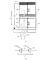
まず、本発明の発光素子の基本的な構成について、図1(a)を用いて説明する。図1
(a)は、基板100上に第1の発光素子110と第2の発光素子120が直列に積層さ
れた、本発明の発光素子の構成例である。第1の発光素子110は、第1の陽極111と
第1の陰極113の間に第1の発光素子の発光層112を有する構造であり、また、第2
の発光素子120は、第2の陽極121と第2の陰極123の間に第2の発光素子の発光
層122を有する構造である。発光層112および122は、いずれも発光性の有機化合
物を含む。
First, the basic configuration of the light emitting element of the present invention will be described with reference to FIG. Figure 1
(A) is a structural example of the light emitting element of the present invention in which the first
The
このような発光素子に対し、第1の陽極111側をプラスに、第2の陰極123側をマ
イナスにバイアスを印加すると、ある電流密度Jの電流が素子に流れる。この時、第1の
陽極111から第1の発光素子の発光層112にホールが、第1の陰極113から第1の
発光素子の発光層112に電子がそれぞれ注入され、再結合に至ることにより、第1の発
光素子から第1の発光130が得られる。また、第2の陽極121から第2の発光素子の
発光層122にホールが、第2の陰極123から第2の発光素子の発光層122に電子が
それぞれ注入され、再結合に至ることにより、第2の発光素子から第2の発光140が得
られる。つまり、第1の発光素子110と第2の発光素子120の両方から発光が得られ
るわけである。
When a bias is applied to such a light emitting element with the
なお、回路的に見れば図1(b)のようになり、第1の発光素子110および第2の発
光素子120に共通の電流密度Jの電流が流れ、それぞれその電流密度Jに対応した輝度
(図1(b)ではそれぞれL1およびL2)で発光することになる。この時、図1(a)
に示した例では、第1の陽極111、第1の陰極113、第2の陽極121を光透過性と
することにより、第1の発光130と第2の発光140の両方を取り出すことができる。
From a circuit point of view, it becomes as shown in FIG. 1B, and a current having a current density J common to the first
In the example shown in FIG. 5, by making the
ここで、本発明においては、第1の発光130および第2の発光140のうちいずれか
一方は、少なくとも2つのピークを有する第1の発光スペクトルを示し、他方はそれと異
なる位置にピークを有する第2の発光スペクトルを示すことが特徴である。例えば、第1
の発光130が青色〜青緑色の波長領域および黄色〜橙色の波長領域の両方にピークを有
する第1の発光スペクトルを示し、第2の発光140が橙色〜赤色の波長領域にピークを
有する第2の発光スペクトルを示すような構成である(詳細は下記実施形態1にて説明す
る)。なお、青色〜青緑色の発光色と黄色〜橙色の発光色は、補色の関係にある発光色で
ある。
Here, in the present invention, one of the
The
発光性の有機化合物が電流によって励起されて発光に至る発光素子では、2つのピーク
を有する発光スペクトル(上述の例では第1の発光スペクトル)を示す発光を得るのは、
従来技術の2波長型白色発光素子に代表されるように比較的容易である。しかしながら、
3つ以上のピークを有する発光スペクトルを得る、あるいはブロードな発光スペクトルを
得るというのは非常に困難である。その技術的課題を克服する手法が、本発明の構成であ
る。すなわち、2波長型白色発光素子のような2つのピークを有する発光スペクトルを示
す発光素子(上述の例では第1の発光素子)をベースに、それだけでは補完しきれない領
域の発光スペクトルを有する発光素子を直列に積層し、発光を重ね合わせる構成である。
この構成であれば、単に1つのピークしか有さない発光素子を直列に積層するよりは、積
層する素子の数を減らすことができ、それに伴って駆動電圧の上昇を抑えることができる
ため有用である。また、図1(b)で示したように、本発明の発光素子においては、ある
電流密度Jに対して得られるL1の輝度とL2の輝度の両方を加算した輝度が得られるた
め、電流に対する輝度(すなわち電流効率)も高い値が得られる。
In a light-emitting element in which a light-emitting organic compound is excited by current and leads to light emission, it is possible to obtain light emission having a light emission spectrum having two peaks (in the above example, the first light emission spectrum)
It is relatively easy as represented by the prior art dual-wavelength white light emitting element. However,
It is very difficult to obtain an emission spectrum having three or more peaks or to obtain a broad emission spectrum. An approach for overcoming the technical problem is the configuration of the present invention. That is, based on a light emitting element showing a light emission spectrum having two peaks (a first light emitting element in the above example) such as a two-wavelength white light emitting element, light emission having an emission spectrum of a region that can not be complemented by itself The elements are stacked in series to overlap light emission.
With this configuration, it is possible to reduce the number of elements to be laminated and to suppress an increase in driving voltage accordingly, rather than laminating the light emitting elements having only one peak in series. is there. Further, as shown in FIG. 1B, in the light emitting device of the present invention, since the luminance obtained by adding both the luminance of L1 and the luminance of L2 obtained for a certain current density J can be obtained, The luminance (i.e. current efficiency) can also be high.
なお、上述の説明では、第1の発光素子110が、少なくとも2つのピークを有する第
1の発光スペクトル示し、第2の発光素子120がそれと異なる位置にピークを有する第
2の発光スペクトルを示す場合を例に説明したが、それとは逆の構成であっても良い。す
なわち、第1の発光素子110が前記第2の発光スペクトルを示し、第2の発光素子12
0が前記第1の発光スペクトルを示しても良い。また、図1(a)では第1の陽極111
側に基板100が設置されている構成としたが、逆に第2の陰極123側に設置されてい
る構成であっても良い。さらに、図1(a)では第1の陽極111側から発光を取り出す
構成としているが、図4(a)に示すように第2の陰極123側から発光を取り出す構成
や、図4(b)に示すようにその両方から発光を取り出す構成であっても良い。
In the above description, the first
0 may indicate the first emission spectrum. Also, in FIG. 1A, the
Although the
以上では、発光層112及び発光層122に発光性の有機化合物を含む場合を説明した
が、発光層は発光性の無機化合物を含んでも良い。つまり110と120を無機のLED
とする。そして、第1の発光130および第2の発光140のうちいずれか一方は、少な
くとも2つのピークを有する第1の発光スペクトルを示し、他方はそれと異なる位置にピ
ークを有する第2の発光スペクトルを示すことを特徴とする。例えば、第1の発光130
が青色〜青緑色の波長領域および黄色〜橙色の波長領域の両方にピークを有する第1の発
光スペクトルを示し、第2の発光140が橙色〜赤色の波長領域にピークを有する第2の
発光スペクトルを示すような構成である。なお、第1の発光スペクトルが有する2つのピ
ークに相当する発光色は補色の関係にある。また、第2の発光スペクトルも補色の関係に
ある2種の波長領域のそれぞれにピークを有してもよい。その場合は、第2の発光スペク
トルは、第1の発光スペクトルを構成するピークとは異なる位置にあるピークを有するの
が好ましい。つまり第1の発光を構成する2種の発光色と第2の発光を構成する2種の発
光色は異なることが好ましい。
Although the case where the
I assume. Then, one of the
Shows a first emission spectrum having a peak in both the blue to bluish green wavelength range and a yellow to orange wavelength range, and a second emission spectrum having a
また、図1に示したような電流によって発光に至る発光素子だけでなく、無機ELのよ
うな衝突励起型の発光素子においても、本願の概念は適用できる。
Further, the concept of the present invention can be applied not only to a light emitting element which emits light by current as shown in FIG. 1, but also to a collision excitation type light emitting element such as inorganic EL.
すなわち、2つの衝突励起型の発光素子を直列に接続する。そして、2つの衝突励起型
の発光素子のうち一方は、少なくとも2つのピークを有する第1の発光スペクトルを示し
、他方はそれと異なる位置にピークを有する第2の発光スペクトルを示すことを特徴とす
る。第1の発光スペクトルが有する2つのピークに対応する発光色は補色の関係にある。
また、第2の発光スペクトルも補色の関係にある2種の波長領域のそれぞれにピークを有
してもよい。その場合は、第2の発光スペクトルは、第1の発光スペクトルを構成するピ
ークとは異なる位置にあるピークを有するのが好ましい。つまり、2つの衝突励起型の発
光素子のうち、一方の発光素子からの発光を構成する2種の発光色と、他方の発光素子か
らの発光を構成する2種の発光色は異なることが好ましい。
That is, two collision excitation light emitting elements are connected in series. One of the two collision-excitation light-emitting elements exhibits a first emission spectrum having at least two peaks, and the other exhibits a second emission spectrum having peaks at different positions. . The emission colors corresponding to the two peaks of the first emission spectrum are in a complementary relationship.
In addition, the second emission spectrum may also have a peak in each of the two wavelength regions in a complementary color relationship. In that case, it is preferable that the second emission spectrum have a peak at a position different from the peak constituting the first emission spectrum. That is, it is preferable that, of the two collision excitation type light emitting elements, the two light emitting colors constituting light emission from one light emitting element and the two light emitting colors constituting light emission from the other light emitting element be different. .
また、補色の関係としては、青色〜青緑色の波長領域と黄色〜橙色の波長領域を例に説
明したが、他の補色の関係(例えば、青緑色〜緑色の波長領域と橙色〜赤色の波長領域)
を用いても良い。また、第1の発光素子の発光色と第2の発光素子の発光色において、そ
れぞれ異なる補色の関係を適用することにより、非常にブロードな白色光を得ることがで
きるため好ましい(詳細は下記実施形態2にて説明する)。
Also, as the complementary color relationship, although the blue to bluish green wavelength region and the yellow to orange wavelength region have been described as an example, other complementary color relationships (for example, bluish green to green wavelength regions and orange to red wavelength) region)
May be used. Also, by applying a different complementary color relationship between the emission color of the first light emitting element and the emission color of the second light emitting element, it is preferable because very broad white light can be obtained (the details will be described below. This will be described in the form 2).
以上で述べたような構成とすることで、可視光領域の多くをカバーでき、高効率な白色
光を容易に得ることができる。次に、以下では、発光色の組み合わせを考慮した構成例を
挙げ、従来技術に対する利点を加えながら説明する。
With the above-described configuration, it is possible to cover much of the visible light range, and it is possible to easily obtain highly efficient white light. Next, in the following, a configuration example in which a combination of luminescent colors is taken into consideration will be described while adding an advantage over the prior art.
[実施形態1]
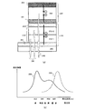
図2(a)に素子構成を示した。図2(a)は、基板200上に第1の発光素子210
と第2の発光素子220が直列に積層された、本発明の発光素子の構成例である。第1の
発光素子210は、第1の陽極211と第1の陰極213の間に第1の発光素子の発光層
212を有する構造であり、また、第2の発光素子220は、第2の陽極221と第2の
陰極223の間に第2の発光素子の発光層222を有する構造である。
Embodiment 1
The element configuration is shown in FIG. 2 (a). FIG. 2A shows the first
And the second
ここで、第1の発光素子の発光層212は、青色〜青緑色の波長領域にピークを有する
発光スペクトルを示す第1の発光層212−1と、黄色〜橙色の波長領域にピークを有す
る発光スペクトルを示す第2の発光層212−2とで構成されている。また、第2の発光
素子の発光層222は橙色〜赤色の波長領域にピークを有する発光スペクトルを示す。な
お、第1の発光層212−1と第2の発光層212−2は逆の積層順であっても良い。
Here, the
このような発光素子に対し、第1の陽極211側をプラスに、第2の陰極223側をマ
イナスにバイアスを印加すると、第1の発光230と第2の発光240が得られる。第1
の発光230は、第1の発光層212−1および第2の発光層212−2の両方からの発
光を合わせたものであるので、図2(b)に示す通り、青色〜青緑色の波長領域および黄
色〜橙色の波長領域の両方にピークを有する発光スペクトルを示す。すなわち、第1の発
光素子は2波長型の白色または白に近い発光色(青みがかった白、黄みがかった白等)を
示すものである。また、第2の発光240は、図2(b)に示す通り、橙色〜赤色の波長
領域にピークを有する発光スペクトルを示す。
When a bias is applied to such a light emitting element with the
The
したがって、本実施形態1における本発明の発光素子は、第1の発光230および第2
の発光240が重ね合わさる結果、青色〜青緑色の波長領域、黄色〜橙色の波長領域、橙
色〜赤色の波長領域をカバーする発光が得られる。
Therefore, the light emitting device of the present invention in the first embodiment includes the
As a result of superimposing the
第1の発光素子は、従来でもよく用いられる補色の関係を用いた2波長型白色発光素子
と同様の構成であり、高輝度かつ素子寿命の良好な白色または白に近い発光色の発光素子
を達成できるが、赤色の波長領域のスペクトルが貧弱であり、カラーフィルターを用いる
フルカラーディスプレイには適さない。しかしながら、本実施形態1のような構成であれ
ば、その課題を十分に克服できることがわかる。
The first light-emitting element has the same configuration as a two-wavelength white light-emitting element using a complementary color relationship often used in the prior art, and has a high luminance and a light-emitting element having a good white or near white emission color. Although this can be achieved, the spectrum in the red wavelength region is poor and not suitable for full color displays using color filters. However, it can be seen that with the configuration as in Embodiment 1, the problem can be sufficiently overcome.
また、例えば、第1の発光層212−1(青色〜青緑色の波長領域にピークを有する発
光スペクトルを示す)の発光輝度が、経時劣化あるいは電流密度により変化したとしても
、スペクトル全体に対する第1の発光層212−1の寄与は1/3程度であるため、色度
のずれは比較的小さくて済むという利点もある。もし従来の2波長型白色発光素子のよう
に、第1の発光素子210のみで構成される発光素子であれば、第1の発光層212−1
の輝度変化は色度に大きな影響を及ぼしてしまう。
Also, for example, even if the emission luminance of the first light emitting layer 212-1 (showing an emission spectrum having a peak in the blue to blue green wavelength region) changes with time or changes with current density, the first Since the contribution of the light emitting layer 212-1 is about 1/3, there is also an advantage that the deviation of the chromaticity may be relatively small. If it is a light emitting element constituted only by the first
The change in luminance of Y greatly affects the chromaticity.
また、青色〜青緑色の波長領域の発光を示す発光素子と、黄色〜橙色の波長領域の発光
を示す発光素子と、橙色〜赤色の波長領域の発光を示す発光素子と、3つの発光素子を直
列に積層させても本実施形態1と同様な発光スペクトルを得ることはできるが、その場合
の駆動電圧は2つの素子を直列に積層した本実施形態1の発光素子に比べ、概ね1.5倍
以上になってしまう。
In addition, a light emitting element that emits light in the blue to bluish green wavelength range, a light emitting element that emits light in the yellow to orange wavelength range, a light emitting element that emits light in the orange to red wavelength range, and three light emitting elements The same emission spectrum as that of Embodiment 1 can be obtained by stacking in series, but the driving voltage in that case is approximately 1.5 as compared with the light emitting element of Embodiment 1 in which two elements are stacked in series. It will be more than doubled.
なお、上述の説明では、第1の発光素子210が2つの発光層(212−1と212−
2)を有するために2つのピークを有する第1の発光スペクトルを示し、第2の発光素子
220はそれと異なる位置にピークを有する第2の発光スペクトルを示す場合を例に説明
したが、第2の発光素子220が前記第1の発光スペクトルを示す構成であっても良い。
すなわち、第2の発光素子220が2つの発光層を有するために2つのピークを有する第
1の発光スペクトルを示し、第1の発光素子210がそれと異なる位置にピークを有する
第2の発光スペクトルを示す構成であっても良い。また、図2(a)では第1の陽極21
1側に基板200が設置されている構成としたが、逆に第2の陰極223側に設置されて
いる構成であっても良い。さらに、図2(a)では第1の陽極211側から発光を取り出
す構成としているが、第2の陰極223側から発光を取り出す構成や、その両方から発光
を取り出す構成であっても良い。
In the above description, the first
Although the first emission spectrum having two peaks to have 2) is shown, and the second emission spectrum having a peak at a different position from that of the second
That is, since the second
Although the
[実施形態2]
図3(a)に素子構成を示した。図3(a)は、基板300上に第1の発光素子310
と第2の発光素子320が直列に積層された、本発明の発光素子の構成例である。第1の
発光素子310は、第1の陽極311と第1の陰極313の間に第1の発光素子の発光層
312を有する構造であり、また、第2の発光素子320は、第2の陽極321と第2の
陰極323の間に第2の発光素子の発光層322を有する構造である。
Second Embodiment
The element configuration is shown in FIG. 3 (a). In FIG. 3A, the first
And the second
ここで、第1の発光素子の発光層312は、青色〜青緑色の波長領域にピークを有する
発光スペクトルを示す第1の発光層312−1と、黄色〜橙色の波長領域にピークを有す
る発光スペクトルを示す第2の発光層312−2とで構成されている。また、第2の発光
素子の発光層222は、青緑色〜緑色の波長領域にピークを有する発光スペクトルを示す
第3の発光層322−1と、橙色〜赤色の波長領域にピークを有する発光スペクトルを示
す第4の発光層322−2とで構成されている。なお、第1の発光層312−1と第2の
発光層312−2は逆の積層順であっても良い。また、第3の発光層322−1と第4の
発光層322−2は逆の積層順であっても良い。
Here, the
このような発光素子に対し、第1の陽極311側をプラスに、第2の陰極323側をマ
イナスにバイアスを印加すると、第1の発光330と第2の発光340が得られる。第1
の発光330は、第1の発光層312−1および第2の発光層312−2の両方からの発
光を合わせたものであるので、図3(b)に示す通り、青色〜青緑色の波長領域および黄
色〜橙色の波長領域の両方にピークを有する発光スペクトルを示す。すなわち、第1の発
光素子は2波長型の白色または白色に近い色の発光を示すものである。また、第2の発光
340は、第3の発光層322−1および第4の発光層322−2の両方からの発光を合
わせたものであるので、図3(b)に示す通り、青緑色〜緑色の波長領域および橙色〜赤
色の波長領域の両方にピークを有する発光スペクトルを示す。すなわち、第2の発光素子
は、第1の発光素子とは異なる2波長型の白色または白色に近い色の発光を示すものであ
る。
When a bias is applied to such a light emitting element with the
The
したがって、本実施形態2における本発明の発光素子は、第1の発光330および第2
の発光340が重ね合わさる結果、青色〜青緑色の波長領域、青緑色〜緑色の波長領域、
黄色〜橙色の波長領域、橙色〜赤色の波長領域をカバーする発光が得られる。
Therefore, the light emitting device of the present invention in the present embodiment 2 has the
As a result of superimposition of the
Light emission covering the yellow to orange wavelength range and the orange to red wavelength range is obtained.
第1の発光素子310および第2の発光素子320はいずれも、従来でもよく用いられ
る補色の関係を用いた2波長型白色発光素子と同様の構成であり、高輝度かつ素子寿命の
良好な白色または白色に近い色の発光素子を達成できるが、第1の発光素子310は主と
して青緑色〜緑色(特にエメラルドグリーン)の波長領域および橙色〜赤色の波長領域の
スペクトルが貧弱であり、カラーフィルターを用いるフルカラーディスプレイには適さな
い。また、エメラルドグリーンの波長領域のスペクトルが小さく、色の鮮やかさにも欠け
る。しかしながら、本実施形態1のような構成であれば、積層した第2の発光素子320
の発光スペクトルによりその欠点を補完でき、課題を十分に克服できることがわかる。
Each of the first
It can be understood that the defect can be complemented by the emission spectrum of and the problem can be sufficiently overcome.
また、例えば、第1の発光層312−1(青色〜青緑色の波長領域にピークを有する発
光スペクトルを示す)の発光輝度が、経時劣化あるいは電流密度により変化したとしても
、スペクトル全体に対する第1の発光層312−1の寄与は1/4程度であるため、色度
のずれは比較的小さくて済むという利点もある。もし従来の2波長型白色発光素子のよう
に、第1の発光素子310のみで構成される発光素子であれば、第1の発光層312−1
の輝度変化は色度に大きな影響を及ぼしてしまう。
Also, for example, even if the emission luminance of the first light emitting layer 312-1 (showing an emission spectrum having a peak in the blue to blue green wavelength region) changes with time or changes with current density, the first Since the contribution of the light emitting layer 312-1 is about 1⁄4, there is also an advantage that the deviation of the chromaticity may be relatively small. If it is a light emitting element constituted only by the first
The change in luminance of Y greatly affects the chromaticity.
また、青色〜青緑色の波長領域の発光を示す発光素子と、青緑色〜緑色の波長領域の発
光を示す発光素子と、黄色〜橙色の波長領域の発光を示す発光素子と、橙色〜赤色の波長
領域の発光を示す発光素子と、4つの発光素子を直列に積層させても本実施形態2と同様
な発光スペクトルを得ることはできるが、その場合の駆動電圧は2つの素子を直列に積層
した本実施形態2の発光素子に比べ、概ね2倍以上にもなってしまう。
In addition, a light emitting element that emits light in the blue to bluish green wavelength range, a light emitting element that emits light in the bluish green to green wavelength range, a light emitting element that emits light in the yellow to orange wavelength range, and orange to red Even if a light emitting element exhibiting light emission in the wavelength range and four light emitting elements are stacked in series, an emission spectrum similar to that of Embodiment 2 can be obtained, but in that case, the driving voltage is two layers stacked in series. Compared to the light emitting device of the second embodiment, the light emitting device is about twice as large.
なお、上述の説明では、第1の発光素子310が青色〜青緑色の波長領域および黄色〜
橙色の波長領域の両方にピークを有するスペクトルを示し、第2の発光素子320は青緑
色〜緑色の波長領域および橙色〜赤色の波長領域の両方にピークを有するスペクトルを示
す場合を例に説明したが、それぞれ逆の関係であっても良い。すなわち、第2の発光素子
320が青色〜青緑色の波長領域および黄色〜橙色の波長領域の両方にピークを有するス
ペクトルを示し、第1の発光素子310が青緑色〜緑色の波長領域および橙色〜赤色の波
長領域の両方にピークを有するスペクトルを示す構成であっても良い。また、図3(a)
では第1の陽極311側に基板300が設置されている構成としたが、逆に第2の陰極3
23側に設置されている構成であっても良い。さらに、図3(a)では第1の陽極311
側から発光を取り出す構成としているが、第2の陰極323側から発光を取り出す構成や
、その両方から発光を取り出す構成であっても良い。
In the above description, the first
The case where a spectrum having peaks in both of the orange wavelength range is shown, and the second
In this case, the
It may be configured to be installed on the 23 side. Furthermore, in FIG. 3A, the
Although light emission is taken out from the side, light emission may be taken out from the side of the
[実施形態3]
次に、以下では、本発明の発光素子の構成、特に図1(a)における第1の発光素子1
10と第2の発光素子120に関し、用いることのできる材料や素子構造を説明する。本
発明の発光素子は、少なくとも図1(a)に示した構成であればよいが、第1の陽極11
1と第1の発光素子の発光層112との間、および第2の陽極121と第2の発光素子の
発光層122との間には、ホール注入層および/またはホール輸送層を挿入していても良
い。また、第1の陰極113と第1の発光素子の発光層112との間、および第2の陰極
123と第2の発光素子の発光層122との間には、電子注入層および/または電子輸送
層を挿入していても良い。
Third Embodiment
Next, in the following, the configuration of the light emitting device of the present invention, in particular, the first light emitting device 1 in FIG.
Materials and element structures that can be used for the
A hole injection layer and / or a hole transport layer is inserted between the light emitting
なお、ホール注入層は陽極からホールを受け取る機能を示す層であり、ホール輸送層は
発光層にホールを受け渡す機能を示す層である。また、電子注入層は陰極から電子を受け
取る機能を示す層であり、電子輸送層は発光層に電子を受け渡す機能を示す層である。
The hole injection layer is a layer showing a function of receiving holes from the anode, and the hole transport layer is a layer showing a function of delivering holes to the light emitting layer. The electron injection layer is a layer showing a function of receiving electrons from the cathode, and the electron transport layer is a layer showing a function of delivering electrons to the light emitting layer.
まず、それら各層に用いることのできる材料を具体的に例示する。ただし、本発明に適
用できる材料は、これらに限定されるものではない。
First, materials that can be used for each of these layers are specifically exemplified. However, materials applicable to the present invention are not limited to these.
ホール注入層に用いることができるホール注入材料としては、フタロシアニン系の化合
物が有効であり、フタロシアニン(略称:H2−Pc)、銅フタロシアニン(略称:Cu
−Pc)、バナジルフタロシアニン(略称:VOPc)等を用いることができる。また、
導電性高分子化合物に化学ドーピングを施した材料もあり、ポリスチレンスルホン酸(略
称:PSS)をドープしたポリエチレンジオキシチオフェン(略称:PEDOT)やポリ
アニリン(略称:PAni)などを用いることもできる。また、酸化モリブデン(MoO
x)、酸化バナジウム(VOx)、酸化ニッケル(NiOx)などの無機半導体の薄膜や、
酸化アルミニウム(Al2O3)などの無機絶縁体の超薄膜も有効である。また、4,4’
,4’’−トリス(N,N−ジフェニル−アミノ)−トリフェニルアミン(略称:TDA
TA)、4,4’,4’’−トリス[N−(3−メチルフェニル)−N−フェニル−アミ
ノ]−トリフェニルアミン(略称:MTDATA)、N,N’−ビス(3−メチルフェニ
ル)−N,N’−ジフェニル−1,1’−ビフェニル−4,4’−ジアミン(略称:TP
D)、4,4’−ビス[N−(1−ナフチル)−N−フェニル−アミノ]−ビフェニル(
略称:α−NPD)、4,4’−ビス[N−(4−(N,N−ジ−m−トリル)アミノ)
フェニル−N−フェニルアミノ]ビフェニル(略称:DNTPD)などの芳香族アミン系
化合物も用いることができる。さらに、それら芳香族アミン系化合物に対してアクセプタ
性を示す物質を芳香族アミン系化合物に添加してもよく、具体的にはVOPcにアクセプ
タである2,3,5,6−テトラフルオロ−7,7,8,8−テトラシアノキノジメタン
(略称:F4−TCNQ)を添加したものや、α−NPDにアクセプタであるMoOxを添
加したものを用いてもよい。
As a hole injection material that can be used for the hole injection layer, phthalocyanine compounds are effective, and phthalocyanine (abbreviation: H 2 -Pc), copper phthalocyanine (abbreviation: Cu)
-Pc), vanadyl phthalocyanine (abbreviation: VOPc) or the like can be used. Also,
There are also materials obtained by subjecting a conductive polymer compound to chemical doping, and polyethylenedioxythiophene (abbreviation: PEDOT) or polyaniline (abbreviation: PAni) doped with polystyrene sulfonic acid (abbreviation: PSS) can also be used. Also, molybdenum oxide (MoO
x), vanadium oxide (VO x), or a thin film of an inorganic semiconductor such as nickel oxide (NiO x),
Ultra thin films of inorganic insulators such as aluminum oxide (Al 2 O 3 ) are also effective. Also, 4,4 '
, 4 ′ ′-tris (N, N-diphenyl-amino) -triphenylamine (abbreviation: TDA)
TA), 4,4 ′, 4 ′ ′-tris [N- (3-methylphenyl) -N-phenyl-amino] -triphenylamine (abbreviation: MTDATA), N, N′-bis (3-methylphenyl) ) -N, N'-diphenyl-1,1'-biphenyl-4,4'-diamine (abbreviation: TP)
D), 4,4′-bis [N- (1-naphthyl) -N-phenyl-amino] -biphenyl (D)
Abbreviations: α-NPD), 4,4′-bis [N- (4- (N, N-di-m-tolyl) amino)
Aromatic amine compounds such as phenyl-N-phenylamino] biphenyl (abbreviation: DNTPD) can also be used. Furthermore, a substance showing acceptor property to these aromatic amine compounds may be added to the aromatic amine compounds, and specifically, 2,3,5,6-tetrafluoro-7 which is an acceptor for VOPc , 7,8,8-tetracyanoquinodimethane (abbreviation: F 4 -TCNQ) may be used, or α-NPD to which MoO x as an acceptor is added may be used.
ホール輸送層に用いることができるホール輸送材料としては、芳香族アミン系化合物が
好適であり、上述したTDATA、MTDATA、TPD、α−NPD、DNTPDなど
を用いることができる。
As a hole transport material that can be used for the hole transport layer, an aromatic amine compound is preferable, and the above-mentioned TDATA, MTDATA, TPD, α-NPD, DNTPD and the like can be used.
電子輸送層に用いることができる電子輸送材料としては、トリス(8−キノリノラト)
アルミニウム(略称:Alq3)、トリス(4−メチル−8−キノリノラト)アルミニウ
ム(略称:Almq3)、ビス(10−ヒドロキシベンゾ[h]−キノリナト)ベリリウ
ム(略称:BeBq2)、ビス(2−メチル−8−キノリノラト)(4−フェニルフェノ
ラト)アルミニウム(略称:BAlq)、ビス[2−(2−ヒドロキシフェニル)ベンゾ
オキサゾラト]亜鉛(略称:Zn(BOX)2)、ビス[2−(2−ヒドロキシフェニル
)ベンゾチアゾラト]亜鉛(略称:Zn(BTZ)2)などの金属錯体が挙げられる。さ
らに、金属錯体以外にも、2−(4−ビフェニリル)−5−(4−tert−ブチルフェ
ニル)−1,3,4−オキサジアゾール(略称:PBD)、1,3−ビス[5−(p−t
ert−ブチルフェニル)−1,3,4−オキサジアゾール−2−イル]ベンゼン(略称
:OXD−7)などのオキサジアゾール誘導体、3−(4−tert−ブチルフェニル)
−4−フェニル−5−(4−ビフェニリル)−1,2,4−トリアゾール(略称:TAZ
)、3−(4−tert−ブチルフェニル)−4−(4−エチルフェニル)−5−(4−
ビフェニリル)−1,2,4−トリアゾール(略称:p−EtTAZ)などのトリアゾー
ル誘導体、2,2’,2”−(1,3,5−ベンゼントリイル)トリス[1−フェニル−
1H−ベンズイミダゾール](略称:TPBI)のようなイミダゾール誘導体、バソフェ
ナントロリン(略称:BPhen)、バソキュプロイン(略称:BCP)などのフェナン
トロリン誘導体を用いることができる。
As an electron transport material that can be used for the electron transport layer, tris (8-quinolinolato)
Aluminum (abbreviation: Alq 3 ), tris (4-methyl-8-quinolinolato) aluminum (abbreviation: Almq 3 ), bis (10-hydroxybenzo [h] -quinolinato) beryllium (abbreviation: BeBq 2 ), bis (2- Methyl-8-quinolinolato) (4-phenylphenolato) aluminum (abbreviation: BAlq), bis [2- (2-hydroxyphenyl) benzoxazolato] zinc (abbreviation: Zn (BOX) 2 ), bis [2- Examples thereof include metal complexes such as (2-hydroxyphenyl) benzothiazolato] zinc (abbreviation: Zn (BTZ) 2 ). Furthermore, in addition to the metal complex, 2- (4-biphenylyl) -5- (4-tert-butylphenyl) -1,3,4-oxadiazole (abbreviation: PBD), 1,3-bis [5-]. (P-t
Oxadiazole derivatives such as ert-butylphenyl) -1,3,4-oxadiazol-2-yl] benzene (abbreviation: OXD-7), 3- (4-tert-butylphenyl)
-4-phenyl-5- (4-biphenylyl) -1,2,4-triazole (abbreviation: TAZ)
), 3- (4-tert-butylphenyl) -4- (4-ethylphenyl) -5- (4-)
Triazole derivatives such as biphenylyl) -1,2,4-triazole (abbreviation: p-EtTAZ), 2,2 ′, 2 ′ ′-(1,3,5-benzenetriyl) tris [1-phenyl-
An imidazole derivative such as 1H-benzimidazole] (abbreviation: TPBI), a phenanthroline derivative such as bathophenanthroline (abbreviation: BPhen), and bathocuproin (abbreviation: BCP) can be used.
電子注入層に用いることができる電子注入材料としては、上述したAlq3、Almq3
、BeBq2、BAlq、Zn(BOX)2、Zn(BTZ)2、PBD、OXD−7、T
AZ、p−EtTAZ、TPBI、BPhen、BCPなどの電子輸送材料を用いること
ができる。その他に、LiF、CsFなどのアルカリ金属ハロゲン化物や、CaF2のよ
うなアルカリ土類ハロゲン化物、Li2Oなどのアルカリ金属酸化物のような絶縁体の超
薄膜がよく用いられる。また、リチウムアセチルアセトネート(略称:Li(acac)
)や8−キノリノラト−リチウム(略称:Liq)などのアルカリ金属錯体も有効である
。また、これら電子注入材料に対してドナー性を示す物質を電子注入材料に添加してもよ
く、ドナーとしてはアルカリ金属、アルカリ土類金属、希土類金属などを用いることがで
きる。具体的にはBCPにドナーであるリチウムを添加したものや、Alq3にドナーで
あるリチウムを添加したものを用いることができる。
As an electron injection material which can be used for the electron injection layer, Alq 3 and Almq 3 mentioned above are used.
, BeBq 2 , BAlq, Zn (BOX) 2 , Zn (BTZ) 2 , PBD, OXD-7, T
Electron transport materials such as AZ, p-EtTAZ, TPBI, BPhen, BCP can be used. Besides, ultra thin films of insulators such as alkali metal halides such as LiF and CsF, alkaline earth halides such as CaF 2 and alkali metal oxides such as Li 2 O are often used. In addition, lithium acetylacetonate (abbreviation: Li (acac)
And alkali metal complexes such as 8-quinolinolato-lithium (abbreviation: Liq) are also effective. In addition, a substance exhibiting a donor property to the electron injecting material may be added to the electron injecting material, and an alkali metal, an alkaline earth metal, a rare earth metal or the like can be used as the donor. Specifically, one obtained by adding lithium which is a donor to BCP or one obtained by adding lithium which is a donor to Alq 3 can be used.
次に、第1の発光素子110や第2の発光素子120における発光層(112や122
)の構成を説明する。まず、発光性の有機化合物として用いることのできる材料を列挙す
るが、本発明においてはこれらに限定されず、いかなる発光性の有機化合物を用いても良
い。
Next, the light emitting layer (112 or 122 in the first
Will be described. First, materials that can be used as the light-emitting organic compound are listed, but the present invention is not limited to these, and any light-emitting organic compound may be used.
例えば青色〜青緑色の発光は、ペリレン、2,5,8,11−テトラ−t−ブチルペリ
レン(略称:TBP)、9,10−ジフェニルアントラセンなどをゲスト材料として用い
、適当なホスト材料に分散させることによって得られる。また、4,4’−ビス(2,2
−ジフェニルビニル)ビフェニル(略称:DPVBi)などのスチリルアリーレン誘導体
や、9,10−ジ−2−ナフチルアントラセン(略称:DNA)、9,10−ビス(2−
ナフチル)−2−t−ブチルアントラセン(略称:t−BuDNA)などのアントラセン
誘導体から得ることができる。また、ポリ(9,9−ジオクチルフルオレン)等のポリマ
ーを用いても良い。
For example, blue to blue green light emission can be dispersed in an appropriate host material using perylene, 2,5,8,11-tetra-t-butylperylene (abbreviation: TBP), 9,10-diphenylanthracene or the like as a guest material It is obtained by In addition, 4,4'-bis (2, 2
Styrylarylene derivatives such as -diphenylvinyl) biphenyl (abbreviation: DPVBi), 9,10-di-2-naphthylanthracene (abbreviation: DNA), 9,10-bis (2-)
It can be obtained from an anthracene derivative such as naphthyl) -2-t-butylanthracene (abbreviation: t-BuDNA). Alternatively, a polymer such as poly (9,9-dioctyl fluorene) may be used.
例えば青緑色〜緑色の発光は、クマリン30、クマリン6などのクマリン系色素や、ビ
ス[2−(2,4−ジフルオロフェニル)ピリジナト]ピコリナトイリジウム(略称:F
Irpic)、ビス(2−フェニルピリジナト)アセチルアセトナトイリジウム(Ir(
ppy)2(acac))などをゲスト材料として用い、適当なホスト材料に分散させる
ことによって得られる。また、上述のペリレンやTBPを5wt%以上の高濃度で適当な
ホスト材料に分散させることによっても得られる。また、BAlq、Zn(BTZ)2、
ビス(2−メチル−8−キノリノラト)クロロガリウム(Ga(mq)2Cl)などの金
属錯体からも得ることができる。また、ポリ(p−フェニレンビニレン)等のポリマーを
用いても良い。
For example, blue-green to green light emission is obtained by using a coumarin-based dye such as coumarin 30 or coumarin 6, or bis [2- (2,4-difluorophenyl) pyridinato] picolina tritium (abbreviation: F
Irpic), bis (2-phenylpyridinato) acetylacetonatoiridium (Ir
It is obtained by using ppy) 2 (acac)) or the like as a guest material and dispersing it in a suitable host material. It can also be obtained by dispersing the above-mentioned perylene or TBP in a suitable host material at a high concentration of 5 wt% or more. Also, BAlq, Zn (BTZ) 2 ,
It can also be obtained from metal complexes such as bis (2-methyl-8-quinolinolato) chlorogallium (Ga (mq) 2 Cl). In addition, a polymer such as poly (p-phenylene vinylene) may be used.
例えば黄色〜橙色の発光は、ルブレン、4−(ジシアノメチレン)−2−[p−(ジメ
チルアミノ)スチリル]−6−メチル−4H−ピラン(略称:DCM1)、4−(ジシア
ノメチレン)−2−メチル−6−(9−ジュロリジル)エチニル−4H−ピラン(略称:
DCM2)、ビス[2−(2−チエニル)ピリジナト]アセチルアセトナトイリジウム(
Ir(thp)2(acac))、ビス(2−フェニルキノリナト)アセチルアセトナト
イリジウム(Ir(pq)2(acac))などをゲスト材料として用い、適当なホスト
材料に分散させることによって得られる。ビス(8−キノキリノラト)亜鉛(略称:Zn
q2)やビス[2−シンナモイル−8−キノリノラト]亜鉛(略称:Znsq2)などの金
属錯体からも得ることができる。また、ポリ(2,5−ジアルコキシ−1,4−フェニレ
ンビニレン)等のポリマーを用いても良い。
For example, yellow to orange luminescence is rubrene, 4- (dicyanomethylene) -2- [p- (dimethylamino) styryl] -6-methyl-4H-pyran (abbreviation: DCM1), 4- (dicyanomethylene) -2 -Methyl-6- (9-durolidyl) ethynyl-4H-pyran (abbreviation:
DCM 2), bis [2- (2-thienyl) pyridinato] acetylacetonatoiridium (
Obtained by dispersing Ir (thp) 2 (acac), bis (2-phenylquinolinato) acetylacetonatoiridium (Ir (pq) 2 (acac)), etc. as a guest material in an appropriate host material . Bis (8-quinoquinolinate) zinc (abbreviation: Zn)
It can also be obtained from metal complexes such as q 2 ) and bis [2-cinnamoyl-8-quinolinolato] zinc (abbreviation: Znsq 2 ). In addition, a polymer such as poly (2,5-dialkoxy-1,4-phenylenevinylene) may be used.
例えば橙色〜赤色の発光は、4−(ジシアノメチレン)−2,6−ビス[p−(ジメチ
ルアミノ)スチリル]−4H−ピラン(略称:BisDCM)、4−(ジシアノメチレン
)−2,6−ビス[2−(ジュロリジン−9−イル)エチニル]−4H−ピランDCM1
)、4−(ジシアノメチレン)−2−メチル−6−(9−ジュロリジル)エチニル−4H
−ピラン(略称:DCM2)、ビス[2−(2−チエニル)ピリジナト]アセチルアセト
ナトイリジウム(Ir(thp)2(acac))、などをゲスト材料として用い、適当
なホスト材料に分散させることによって得られる。ビス(8−キノキリノラト)亜鉛(略
称:Znq2)やビス[2−シンナモイル−8−キノリノラト]亜鉛(略称:Znsq2)
などの金属錯体からも得ることができる。また、ポリ(3−アルキルチオフェン)等のポ
リマーを用いても良い。
For example, orange to red light emission can be obtained by using 4- (dicyanomethylene) -2,6-bis [p- (dimethylamino) styryl] -4H-pyran (abbreviation: BisDCM), 4- (dicyanomethylene) -2,6- Bis [2- (durolidin-9-yl) ethynyl] -4H-pyran DCM1
), 4- (dicyanomethylene) -2-methyl-6- (9-durolidyl) ethynyl-4H
By dispersing it in a suitable host material using pyrane (abbreviation: DCM2), bis [2- (2-thienyl) pyridinato] acetylacetonatoiridium (Ir (thp) 2 (acac)), etc. as a guest material can get. Bis (8-quinoquinolinato) zinc (abbreviation: Znq 2 ) or bis [2-cinnamoyl-8-quinolinolato] zinc (abbreviation: Znsq 2 )
Can also be obtained from metal complexes such as In addition, a polymer such as poly (3-alkylthiophene) may be used.
なお、上記の構成において、適当なホスト材料としては、発光性の有機化合物よりも発
光色が短波長のものであるか、またはエネルギーギャップの大きいものであればよい。具
体的には、上述した例に代表されるホール輸送材料や電子輸送材料から適宜選択すること
ができる。また、4,4’−ビス(N−カルバゾリル)ビフェニル(略称:CBP)、4
,4’,4’’−トリス(N−カルバゾリル)トリフェニルアミン(略称:TCTA)、
1,3,5−トリス[4−(N−カルバゾリル)フェニル]ベンゼン(略称:TCPB)
などを使用しても良い。
In the above configuration, as a suitable host material, it may be one having a shorter emission wavelength or a larger energy gap than the light-emitting organic compound. Specifically, it can be appropriately selected from hole transporting materials and electron transporting materials represented by the above-mentioned examples. In addition, 4,4′-bis (N-carbazolyl) biphenyl (abbreviation: CBP), 4
, 4 ′, 4 ′ ′-tris (N-carbazolyl) triphenylamine (abbreviation: TCTA),
1,3,5-tris [4- (N-carbazolyl) phenyl] benzene (abbreviation: TCPB)
You may use etc.
一方、本発明の発光素子における陽極(第1の陽極111および第2の陽極121)材
料としては、仕事関数の大きい導電性材料を用いることが好ましい。また、第1の陽極1
11から光を取り出す場合は、第1の陽極111はインジウムスズ酸化物(ITO)、イ
ンジウム亜鉛酸化物(IZO)、酸化亜鉛(ZnO)、酸化ケイ素を添加したインジウム
錫酸化物等の透明導電性材料を用いればよい。また、第1の陽極111側を遮光性とする
のであれば、第1の陽極111はTiN、ZrN、Ti、W、Ni、Pt、Cr等の単層
膜の他、窒化チタンとアルミニウムを主成分とする膜との積層、窒化チタン膜とアルミニ
ウムを主成分とする膜と窒化チタン膜との三層構造等を用いることができる。あるいは、
Ti、Al等の反射性電極の上に上述した透明導電性材料を積層する方法でもよい。また
、第2の陽極121は光透過性が必要であり、ITO、IZO、ZnOなどの透明導電性
材料の他、上述したホール輸送性の化合物(特に芳香族アミン系化合物)に対してアクセ
プタ性を示す物質をホール輸送性の化合物に添加した構成を用いても良い。具体的にはV
OPcにアクセプタである2,3,5,6−テトラフルオロ−7,7,8,8−テトラシ
アノキノジメタン(略称:F4−TCNQ)を添加したものや、α−NPDにアクセプタ
であるMoOxを添加したものを第2の陽極121として用いてもよい。
On the other hand, as a material of the anode (the
In the case of extracting light from 11, the
Alternatively, the above-described transparent conductive material may be laminated on a reflective electrode such as Ti or Al. Further, the
One obtained by adding 2,3,5,6-tetrafluoro-7,7,8,8-tetracyanoquinodimethane (abbreviation: F 4 -TCNQ) as an acceptor to OPc, or one as an acceptor to α-NPD What added MoO x may be used as the
また、陰極(第1の陰極113および第2の陰極123)材料としては、仕事関数の小
さい導電性材料を用いることが好ましく、具体的には、LiやCs等のアルカリ金属、お
よびMg、Ca、Sr等のアルカリ土類金属、およびこれらを含む合金(Mg:Ag、A
l:Liなど)の他、YbやEr等の希土類金属を用いて形成することもできる。また、
LiF、CsF、CaF2、Li2O等の電子注入層を用いる場合は、アルミニウム等の通
常の導電性薄膜を用いることができる。また、第2の陰極123側を光の取り出し方向と
する場合は、LiやCs等のアルカリ金属、およびMg、Ca、Sr等のアルカリ土類金
属を含む超薄膜と、透明導電膜(ITO、IZO、ZnO等)との積層構造を用いればよ
い。あるいは、上述した電子輸送材料に対してドナー性を示す物質(アルカリ金属または
アルカリ土類金属など)を添加した構成を用い、その上に透明導電膜(ITO、IZO、
ZnO等)を積層してもよい。また、第1の陰極113は光透過性が必要であり、上述し
た電子輸送材料に対してドナー性を示す物質(アルカリ金属またはアルカリ土類金属など
)を電子輸送材料に添加した構成を用いても良い。具体的にはBCPにドナーであるリチ
ウムを添加したものや、Alq3にドナーであるリチウムを添加したものを用いることが
できる。
In addition, as a material of the cathode (the
In addition to l) Li and the like, rare earth metals such as Yb and Er can also be used. Also,
LiF, CsF, in the case of using an electron injecting layer such as CaF 2, Li 2 O, may be used usual conductive thin film such as aluminum. When the
ZnO or the like may be stacked. In addition, the
なお、以上で述べた本発明の発光素子を作製するに当たっては、発光素子中の各層の積
層法を限定されるものではない。積層が可能ならば、真空蒸着法やスピンコート法、イン
クジェット法、ディップコート法など、どの様な手法を選んでも良いものとする。
In addition, in manufacturing the light emitting element of this invention described above, the lamination | stacking method of each layer in a light emitting element is not limited. As long as lamination is possible, any method such as vacuum deposition, spin coating, ink jet, dip coating, etc. may be selected.
以下に、本発明の実施例について説明する。 Hereinafter, examples of the present invention will be described.
本実施例では、本発明の発光素子の素子構造および作製方法について、図5を用いて具
体的に説明する。
In this example, the element structure and the manufacturing method of the light emitting element of the present invention will be specifically described with reference to FIGS.
まず、110nmの膜厚でインジウム錫酸化物(ITO)が成膜されたガラス基板50
0を用意する。成膜されたITOは、本実施例において第1の陽極511として作用する
。
First, a glass substrate 50 on which indium tin oxide (ITO) was deposited to a film thickness of 110 nm
Prepare 0. The deposited ITO acts as a
次に、第1の陽極511が形成されたガラス基板500を、第1の陽極511が形成さ
れた面が下方になるように真空蒸着装置内の基板ホルダーに固定する。そして、真空蒸着
法により、第1の陽極511上に膜厚が20nmとなるようにCuPcを成膜し、ホール
注入層512を形成する。真空蒸着は、真空蒸着装置の内部に備えられた蒸発源にCuP
cを入れ、抵抗加熱法により蒸発させることによって行う。なお、本実施例においては、
ホール注入層512はホール輸送層としても機能する。
Next, the
c by charging and evaporating by resistance heating. In the present embodiment,
The
次いで、ホール注入層512上に、第1の発光素子の発光層513を形成する。本実施
例においては、第1の発光素子の発光層513は、第1の発光層513−1および第2の
発光層513−2から構成されており、第1の発光層513−1と第2の発光層513−
2とは互いに接している。
Then, the
2 is in contact with each other.
第1の発光層513−1はα−NPDとペリレンとを含む構成であり、α−NPDとペ
リレンとをそれぞれ蒸発源として用いた共蒸着法にて形成する。この時、α−NPD中に
ペリレンが3質量%の割合で含まれるように調節する。膜厚は30nmとする。この第1
の発光層513−1においては、ペリレンが青色〜青緑色の発光を示す発光性の有機化合
物として機能する。
The first light emitting layer 513-1 is a structure including α-NPD and perylene, and is formed by a co-evaporation method using α-NPD and perylene as evaporation sources. At this time, perylene is adjusted to be contained at a rate of 3% by mass in α-NPD. The film thickness is 30 nm. This first
In the light-emitting layer 513-1, perylene functions as a light-emitting organic compound that emits blue to bluish green light.
また、第2の発光層513−2はDNAとDCM2とを含む構成であり、DNAとDC
M2とをそれぞれ蒸発源として備えた共蒸着法にて形成する。この時、DNA中にDCM
2が0.1質量%の割合で含まれるように調節する。膜厚は30nmとする。この第2の
発光層513−2においては、DCM2が黄色〜橙色の発光を示す発光性の有機化合物と
して機能する。
Further, the second light emitting layer 513-2 is a structure including DNA and DCM2, and the DNA and DC
It forms by the co-evaporation method which equipped M2 as an evaporation source, respectively. At this time, DCM in DNA
Adjust 2 to be included at a rate of 0.1% by mass. The film thickness is 30 nm. In the second light-emitting layer 513-2, DCM2 functions as a light-emitting organic compound that emits yellow to orange light.
次に、第1の発光素子の発光層513上に、膜厚が10nmとなるようにBCPを成膜
し、電子輸送層514を形成する。次いで、電子輸送層514上に、膜厚が20nmとな
るようにAlq3を成膜し、電子注入層515を形成する。これらの成膜に関しても、ホ
ール注入層512の形成と同様に、真空蒸着法によって行う。
Next, a BCP film is formed to a thickness of 10 nm over the
さらに、電子注入層515上に、第1の陰極516を形成する。第1の陰極516は、
電子輸送性の化合物であるBCPと、それに対してドナー性を示す物質であるリチウムと
を含む構成であり、BCPとリチウムとをそれぞれ蒸発源として備えた共蒸着法にて形成
する。この時、BCP中にリチウムが0.5質量%の割合で含まれるように調節する。膜
厚は10nmとする。
Further, a
It is configured to include BCP, which is an electron transporting compound, and lithium, which is a substance exhibiting a donor property, and is formed by a co-evaporation method in which BCP and lithium are provided as evaporation sources. At this time, lithium is adjusted to be contained at a rate of 0.5% by mass in BCP. The film thickness is 10 nm.
このようにして第1の発光素子510を形成した後、第2の発光素子520を直列に積
層する。まず第2の陽極521は、MoOxを10nmの膜厚で成膜することにより形成
する。成膜は、ホール注入層512の形成と同様に、真空蒸着法によって行う。
After the first
次に、第2の陽極521上に、膜厚が50nmとなるようにα−NPDを成膜し、ホー
ル注入層522を形成する。なお、本実施例においては、ホール注入層522はホール輸
送層としても機能する。成膜は、ホール注入層512の形成と同様に、真空蒸着法によっ
て行う。
Next, on the
次いで、ホール注入層522上に、第2の発光素子の発光層523を形成する。第2の
発光素子の発光層523はCBPとIr(btp)2(acac)とを含む構成であり、
CBPとIr(btp)2(acac)とをそれぞれ蒸発源として備えた共蒸着法にて形
成する。この時、CBP中にIr(btp)2(acac)が8質量%の割合で含まれる
ように調節する。膜厚は30nmとする。この第2の発光素子の発光層523においては
、Ir(btp)2(acac)が、第1の発光素子の発光色とは異なる発光色を示す発
光性の有機化合物として機能する。
Next, the
CBP and Ir (btp) 2 (acac) are respectively formed by a co-evaporation method provided as evaporation sources. At this time, CBP is adjusted so that Ir (btp) 2 (acac) is contained at a rate of 8% by mass. The film thickness is 30 nm. In the light-emitting
次に、第2の発光素子の発光層523上に、膜厚が10nmとなるようにBCPを成膜
し、電子輸送層524を形成する。次いで、電子輸送層524上に、膜厚が20nmとな
るようにAlq3を成膜し、電子注入層525を形成する。これらの成膜に関しても、ホ
ール注入層512の形成と同様に、真空蒸着法によって行う。
Next, a BCP film is formed to a thickness of 10 nm over the
さらに、電子注入層525上に、第2の陰極526を形成する。第2の陰極526は、
電子輸送性の化合物であるBCPと、それに対してドナー性を示す物質であるリチウムと
を含む構成であり、BCPとリチウムとをそれぞれ蒸発源として備えた共蒸着法にて形成
する。この時、BCP中にリチウムが0.5質量%の割合で含まれるように調節する。膜
厚は10nmとする。さらにAlを150nmの膜厚で蒸着することにより、第2の陰極
526とする。
Further, a
It is configured to include BCP, which is an electron transporting compound, and lithium, which is a substance exhibiting a donor property, and is formed by a co-evaporation method in which BCP and lithium are provided as evaporation sources. At this time, lithium is adjusted to be contained at a rate of 0.5% by mass in BCP. The film thickness is 10 nm. Further, Al is deposited to a thickness of 150 nm to form a
以上のようにして形成された第1の発光素子510は、青色〜青緑色の発光を示す第1
の発光層と黄色〜橙色の発光を示す第2の発光層を有しているため、青色〜青緑色の波長
領域と黄色〜橙色の波長領域の2箇所に発光スペクトルのピークを示す。また、第2の発
光素子520は赤色の発光を示すため、第1の発光素子とは異なる位置にピークを有する
発光スペクトルを示す。
The first light-emitting
Since it has the 2nd light emitting layer which shows the light emission layer and yellow-orange light emission of the light emitting layer, the peak of a light emission spectrum is shown in two places of a blue-bluish green wavelength range and a yellow-orange wavelength range. In addition, since the second light-emitting
したがって、第1の発光素子510および第2の発光素子520を直列に積層した本実
施例の発光素子は、第1の陽極511と第2の陰極526との間に電圧を印加することに
より、青色〜青緑色の波長領域、黄色〜橙色の波長領域、そして赤色の波長領域を広範囲
にカバーするブロードな白色発光が得られる。また、3つの発光色のうちいずれかの輝度
が経時劣化あるいは電流密度により変化したとしても、スペクトルがブロードである影響
で色度のずれは比較的小さい。
Therefore, by applying a voltage between the
本実施例では、本発明の発光素子の素子構造および作製方法について、図6を用いて具
体的に説明する。
Example 1 In this example, an element structure and a manufacturing method of a light emitting element of the present invention will be specifically described with reference to FIGS.
まず、110nmの膜厚でインジウム錫酸化物(ITO)が成膜されたガラス基板60
0を用意する。成膜されたITOは、本実施例において第1の陽極611として作用する
。
First, a glass substrate 60 on which indium tin oxide (ITO) was deposited to a film thickness of 110 nm
Prepare 0. The deposited ITO acts as a
次に、第1の陽極611が形成されたガラス基板600を、第1の陽極611が形成さ
れた面が下方になるように真空蒸着装置内の基板ホルダーに固定する。そして、真空蒸着
法により、第1の陽極611上に膜厚が20nmとなるようにDNTPDを成膜し、ホー
ル注入層612を形成する。真空蒸着は、真空蒸着装置の内部に備えられた蒸発源にDN
TPDを入れ、抵抗加熱法により蒸発させることによって行う。
Next, the
It is done by putting TPD and evaporating it by resistance heating method.
次いで、ホール注入層612上に、膜厚が20nmとなるようにα−NPDを成膜し、
ホール輸送層613を形成する。成膜は、ホール注入層612の形成と同様に、真空蒸着
法によって行う。
Then, on the
A
次に、ホール輸送層613上に、第1の発光素子の発光層614を形成する。本実施例
においては、第1の発光素子の発光層614は、第1の発光層614−1および第2の発
光層614−2から構成されており、第1の発光層614−1と第2の発光層614−2
とは互いに接している。
Next, the
And are in contact with each other.
第1の発光層614−1はα−NPDとTBPとを含む構成であり、α−NPDとTB
Pとをそれぞれ蒸発源として用いた共蒸着法にて形成する。この時、α−NPD中にTB
Pが1質量%の割合で含まれるように調節する。膜厚は10nmとする。この第1の発光
層614−1においては、TBPが青色〜青緑色の発光を示す発光性の有機化合物として
機能する。
The first light emitting layer 614-1 has a configuration including α-NPD and TBP, and α-NPD and TB.
It forms by the co-evaporation method which used P and each as an evaporation source. At this time, TB during α-NPD
Adjust so that P is contained at a rate of 1% by mass. The film thickness is 10 nm. In the first light emitting layer 614-1, TBP functions as a light emitting organic compound which emits blue to bluish green light.
また、第2の発光層614−2はα−NPDとDCM2とを含む構成であり、α−NP
DとDCM2とをそれぞれ蒸発源として備えた共蒸着法にて形成する。この時、α−NP
D中にDCM2が1質量%の割合で含まれるように調節する。膜厚は10nmとする。こ
の第2の発光層614−2においては、DCM2が黄色〜橙色の発光を示す発光性の有機
化合物として機能する。
In addition, the second light emitting layer 614-2 includes α-NPD and DCM2, and α-NP
It forms by the co-evaporation method which equipped D and DCM2 as an evaporation source, respectively. At this time, α-NP
Adjust so that DCM 2 is contained in the proportion of 1% by mass in D. The film thickness is 10 nm. In the second light-emitting layer 614-2, DCM2 functions as a light-emitting organic compound that emits yellow to orange light.
次に、第1の発光素子の発光層614上に、膜厚が20nmとなるようにBAlqを成
膜し、電子輸送層615を形成する。次いで、電子輸送層615上に、膜厚が30nmと
なるようにAlq3を成膜し、電子注入層616を形成する。これらの成膜に関しても、
ホール注入層612の形成と同様に、真空蒸着法によって行う。
Next, BAlq is formed to a thickness of 20 nm over the light-emitting
Similar to the formation of the
さらに、電子注入層616上に、第1の陰極617を形成する。第1の陰極617は、
電子輸送性の化合物であるBCPと、それに対してドナー性を示す物質であるリチウムと
を含む構成であり、BCPとリチウムとをそれぞれ蒸発源として備えた共蒸着法にて形成
する。この時、BCP中にリチウムが0.5質量%の割合で含まれるように調節する。膜
厚は10nmとする。
Further, a
It is configured to include BCP, which is an electron transporting compound, and lithium, which is a substance exhibiting a donor property, and is formed by a co-evaporation method in which BCP and lithium are provided as evaporation sources. At this time, lithium is adjusted to be contained at a rate of 0.5% by mass in BCP. The film thickness is 10 nm.
このようにして第1の発光素子610を形成した後、第2の発光素子620を直列に積
層する。まず第2の陽極621は、ホール輸送性の化合物であるα−NPDと、それに対
してアクセプタ性を示す物質であるMoOxとを含む構成であり、α−NPDとMoOxと
をそれぞれ蒸発源として備えた共蒸着法にて形成する。この時、α−NPD中にMoOx
が25質量%の割合で含まれるように調節する。膜厚は50nmとする。
After the first
Is adjusted to be contained at a rate of 25% by mass. The film thickness is 50 nm.
次に、第2の陽極621上に膜厚が25nmとなるようにα−NPDを成膜し、ホール
注入層622を形成する。成膜は、ホール注入層612の形成と同様に、真空蒸着法によ
って行う。なお、本実施例においては、ホール注入層622はホール輸送層としても機能
する。
Next, α-NPD is deposited over the
次いで、ホール注入層622上に、第2の発光素子の発光層623を形成する。本実施
例においては、第2の発光素子の発光層623は、第3の発光層623−1および第4の
発光層623−2から構成されており、第3の発光層623−1と第4の発光層623−
2とは互いに接している。
Next, the
2 is in contact with each other.
第3の発光層623−1はα−NPDとBisDCMとを含む構成であり、α−NPD
とBisDCMとをそれぞれ蒸発源として備えた共蒸着法にて形成する。この時、α−N
PD中にBisDCMが2質量%の割合で含まれるように調節する。膜厚は15nmとす
る。この第3の発光層623−1においては、BisDCMが橙色〜赤色(特に赤色)の
発光を示す発光性の有機化合物として機能する。
The third light emitting layer 623-1 is configured to include α-NPD and BisDCM, and α-NPD
And BisDCM, respectively, by co-evaporation method equipped as an evaporation source. At this time, α-N
Adjust so that 2% by mass of BisDCM is contained in PD. The film thickness is 15 nm. In the third light-emitting layer 623-1, BisDCM functions as a light-emitting organic compound that emits orange to red light (in particular, red).
また、第4の発光層623−2は、20nmの膜厚でGa(mq)2Clを成膜するこ
とにより形成する。成膜は、ホール注入層622の形成と同様に、真空蒸着法によって行
う。この第4の発光層623−2においては、Ga(mq)2Clが青緑色〜緑色(特に
エメラルドグリーン)の発光を示す発光性の有機化合物として機能する。
The fourth light emitting layer 623-2 is formed by depositing Ga (mq) 2 Cl to a thickness of 20 nm. The film formation is performed by vacuum evaporation similarly to the formation of the
次に、第2の発光素子の発光層623上に、膜厚が55nmとなるようにAlq3を成
膜し、電子注入層624を形成する。成膜は、ホール注入層612の形成と同様に、真空
蒸着法によって行う。なお、本実施例においては、電子注入層624は電子輸送層として
も機能する。
Next, Alq 3 is deposited to a thickness of 55 nm over the light-emitting
さらに、電子注入層624上に、第2の陰極625を形成する。第2の陰極625は、
電子輸送性の化合物であるBCPと、それに対してドナー性を示す物質であるリチウムと
を含む構成であり、BCPとリチウムとをそれぞれ蒸発源として備えた共蒸着法にて形成
する。この時、BCP中にリチウムが0.5質量%の割合で含まれるように調節する。膜
厚は10nmとする。さらにAlを150nmの膜厚で蒸着することにより、第2の陰極
625とする。
Further, a
It is configured to include BCP, which is an electron transporting compound, and lithium, which is a substance exhibiting a donor property, and is formed by a co-evaporation method in which BCP and lithium are provided as evaporation sources. At this time, lithium is adjusted to be contained at a rate of 0.5% by mass in BCP. The film thickness is 10 nm. Further, Al is deposited to a thickness of 150 nm to form a
以上のようにして形成された第1の発光素子610は、青色〜青緑色の発光を示す第1
の発光層と黄色〜橙色の発光を示す第2の発光層を有しているため、青色〜青緑色の波長
領域と黄色〜橙色の波長領域の2箇所に発光スペクトルのピークを示す。また、第2の発
光素子620は、青緑色〜緑色の発光を示す第3の発光層と橙色〜赤色の発光を示す第4
の発光層を有しているため、青緑色〜緑色の波長領域と橙色〜赤色の波長領域の2箇所に
発光スペクトルのピークを示す。
The first
Since it has the 2nd light emitting layer which shows the light emission layer and yellow-orange light emission of the light emitting layer, the peak of a light emission spectrum is shown in two places of a blue-bluish green wavelength range and a yellow-orange wavelength range. In addition, the second
Since the light emitting layer has the light emitting layer, the peaks of the light emission spectrum are shown at two points of the blue green to green wavelength region and the orange to red wavelength region.
したがって、第1の発光素子610および第2の発光素子620を直列に積層した本実
施例の発光素子は、第1の陽極611と第2の陰極625との間に電圧を印加することに
より、青色〜青緑色の波長領域、黄色〜橙色の波長領域、および青緑色〜緑色、橙色〜赤
色の波長領域、すなわちほぼ可視光領域全般をカバーするブロードな白色発光が得られる
。特に、第1の発光素子のみを使った白色では十分な輝度が得られないエメラルドグリー
ンと赤色の波長領域で、十分な輝度を達成できることが大きな利点である。また、4つの
発光色のうちいずれかの輝度が経時劣化あるいは電流密度により変化したとしても、スペ
クトルがブロードである影響で色度のずれは比較的小さい。
Therefore, the light emitting element of this embodiment in which the first
本実施例では、本発明の発光素子を有する発光装置について図7を用いて説明する。な
お、図7(A)は発光装置を示す上面図、図7(B)は図7(A)をA−A’で切断した
断面図である。点線で示された701は駆動回路部(ソース側駆動回路)、702は画素
部、703は駆動回路部(ゲート側駆動回路)である。また、704は封止基板、705
はシール材であり、シール材705で囲まれた内側である707は、空間になっている。
In this embodiment, a light emitting device having a light emitting element of the present invention will be described with reference to FIG. 7A is a top view of the light emitting device, and FIG. 7B is a cross-sectional view of FIG. 7A taken along a line A-A '. Reference numeral 701 shown by a dotted line is a drive circuit portion (source side drive circuit), 702 is a pixel portion, and 703 is a drive circuit portion (gate side drive circuit). Further, 704 is a sealing substrate, 705
Is a sealing material, and an inner side 707 surrounded by the sealing
なお、708はソース側駆動回路701及びゲート側駆動回路703に入力される信号
を伝送するための配線であり、外部入力端子となるFPC(フレキシブルプリントサーキ
ット)709からビデオ信号、クロック信号、スタート信号、リセット信号等を受け取る
。なお、ここではFPCしか図示されていないが、このFPCにはプリント配線基板(P
WB)が取り付けられていても良い。本明細書における発光装置には、発光装置本体だけ
でなく、それにFPCもしくはPWBが取り付けられた状態をも含むものとする。
Reference numeral 708 denotes a wiring for transmitting signals input to the source side drive circuit 701 and the gate side drive circuit 703, and a video signal, a clock signal, and a start signal from an FPC (flexible printed circuit) 709 serving as an external input terminal. , Reset signal etc. Although only the FPC is shown here, a printed wiring board (P
WB) may be attached. The light emitting device in the present specification includes not only the light emitting device main body but also a state in which an FPC or a PWB is attached thereto.
次に、断面構造について図7(B)を用いて説明する。素子基板710上には駆動回路
部及び画素部が形成されているが、ここでは、駆動回路部であるソース側駆動回路701
と、画素部702が示されている。
Next, the cross-sectional structure will be described with reference to FIG. Although a driver circuit portion and a pixel portion are formed over the
And the pixel portion 702 is shown.
なお、ソース側駆動回路701はnチャネル型TFT723とpチャネル型TFT72
4とを組み合わせたCMOS回路が形成される。また、駆動回路を形成する回路は、公知
のCMOS回路、PMOS回路もしくはNMOS回路で形成しても良い。また、本実施例
では、基板上に駆動回路を形成したドライバー一体型を示すが、必ずしもその必要はなく
、基板上ではなく外部に駆動回路を形成することもできる。
The source driver circuit 701 includes an n-
A CMOS circuit in combination with 4 is formed. Further, the circuit forming the drive circuit may be formed by a known CMOS circuit, a PMOS circuit or an NMOS circuit. Further, although the driver integrated type in which the drive circuit is formed on the substrate is shown in the present embodiment, it is not always necessary, and the drive circuit can be formed not on the substrate but outside.
また、画素部702はスイッチング用TFT711と、電流制御用TFT712とその
ドレインに電気的に接続された陽極713とを含む複数の画素により形成される。なお、
陽極713の端部を覆って絶縁物714が形成されている。ここでは、ポジ型の感光性ア
クリル樹脂膜を用いることにより形成する。
The pixel portion 702 is formed of a plurality of pixels including a switching
An insulator 714 is formed to cover the end of the anode 713. Here, it is formed by using a positive photosensitive acrylic resin film.
また、膜被覆性を良好なものとするため、絶縁物714の上端部または下端部に曲率を
有する曲面が形成されるようにする。例えば、絶縁物714の材料としてポジ型の感光性
アクリルを用いた場合、絶縁物714の上端部のみに曲率半径(0.2μm〜3μm)を
有する曲面を持たせることが好ましい。また、絶縁物714として、感光性の光によって
エッチャントに不溶解性となるネガ型、或いは光によってエッチャントに溶解性となるポ
ジ型のいずれも使用することができ、有機化合物に限らず無機化合物、例えば、酸化珪素
、酸窒化珪素等、の両者を使用することができる。
In addition, a curved surface having a curvature is formed at the upper end portion or the lower end portion of the insulator 714 in order to improve the film coverage. For example, when positive photosensitive acrylic is used as the material of the insulator 714, it is preferable that only the upper end portion of the insulator 714 have a curved surface with a curvature radius (0.2 μm to 3 μm). Further, as the insulator 714, any of negative type which becomes insoluble in etchant by photosensitive light or positive type which becomes soluble in etchant by light can be used, and not only organic compounds but inorganic compounds, For example, both silicon oxide and silicon oxynitride can be used.
陽極713上には、本発明の発光素子715および陰極716がそれぞれ形成されてい
る。ここで、陽極713に用いる材料としては、仕事関数の大きい材料を用いることが望
ましい。例えば、ITO(インジウムスズ酸化物)膜、ITSO(indium tin
silicon oxide)、インジウム亜鉛酸化物(IZO)膜、窒化チタン膜、
クロム膜、タングステン膜、Zn膜、Pt膜などの単層膜の他、窒化チタンとアルミニウ
ムを主成分とする膜との積層、窒化チタン膜とアルミニウムを主成分とする膜と窒化チタ
ン膜との3層構造等を用いることができる。また、陽極713をITO膜とし、陽極71
3と接続する電流制御用TFT712の配線を、窒化チタン、アルミニウムを主成分とす
る膜との積層構造、または窒化チタン膜、アルミニウムを主成分とする膜、窒化チタン膜
との積層構造とすると、配線としての抵抗も低く、ITO膜との良好なオーミックコンタ
クトがとれ、さらに陽極713を陽極として機能させることができる。また、陽極713
は、本発明の発光素子715における第1の陽極と同一の物質で形成されていても良い。
もしくは、陽極713は発光素子715の第1の陽極と一体化されていても良い。
The light emitting element 715 and the cathode 716 of the present invention are formed on the anode 713, respectively. Here, as a material used for the anode 713, it is desirable to use a material having a large work function. For example, ITO (indium tin oxide) film, ITSO (indium tin)
silicon oxide), indium zinc oxide (IZO) film, titanium nitride film,
In addition to a single layer film such as a chromium film, a tungsten film, a Zn film, or a Pt film, a lamination of a film containing titanium nitride and aluminum as a main component, a titanium nitride film and a film containing aluminum as a main component, and a titanium nitride film A three-layer structure or the like can be used. The anode 713 is an ITO film, and the anode 71 is
Assuming that the wiring of the current control TFT 712 connected to 3 is a stacked structure of titanium nitride and a film containing aluminum as a main component, or a stacked structure of a titanium nitride film, a film containing aluminum as a main component, and a titanium nitride film, The resistance as a wiring is also low, good ohmic contact with the ITO film can be obtained, and the anode 713 can function as an anode. Also, the anode 713
May be formed of the same material as the first anode in the light emitting element 715 of the present invention.
Alternatively, the anode 713 may be integrated with the first anode of the light emitting element 715.
また、本発明の発光素子715は、図1で示したような第1の発光素子110と第2の
発光素子120を積層した構成であり、具体的には実施形態、実施例1および実施例2の
如き構成である。
The light emitting element 715 according to the present invention has a configuration in which the first
さらに、陰極716に用いる材料としては、仕事関数の小さい材料(Al、Ag、Li
、Ca、またはこれらの合金MgAg、MgIn、AlLi、CaF2、またはCaN)
を用いればよいが、これらに限定されることはなく、適切な電子注入材料を選択すること
により、多様な導電膜を適用することができる。なお、本発明の発光素子715から出た
光を陰極716を透過させる場合には、陰極716として、膜厚を薄くした金属薄膜と、
透明導電膜ITO(酸化インジウム酸化スズ合金)、ITSO(indium tin
silicon oxide)、酸化インジウム酸化亜鉛合金(In2O3―ZnO)、酸
化亜鉛(ZnO)等)との積層を用いる手法が考えられる。また、陰極716は、本発明
の発光素子715における第2の陰極と同一の物質で形成されていても良い。もしくは、
陰極716は発光素子715の第2の陰極と一体化されていても良い。
Furthermore, as a material used for the cathode 716, a material having a small work function (Al, Ag, Li
, Ca, or their alloys MgAg, MgIn, AlLi, CaF 2 or CaN)
However, the present invention is not limited to these, and various conductive films can be applied by selecting an appropriate electron injecting material. In the case where light emitted from the light emitting element 715 of the present invention is transmitted through the cathode 716, a metal thin film with a thin film thickness is used as the cathode 716;
Transparent conductive film ITO (indium oxide tin oxide alloy), ITSO (indium tin)
A method using lamination with silicon oxide), indium oxide-zinc oxide alloy (In 2 O 3 -ZnO), zinc oxide (ZnO) or the like can be considered. In addition, the cathode 716 may be formed of the same material as the second cathode in the light-emitting element 715 of the present invention. Or
The cathode 716 may be integrated with the second cathode of the light emitting element 715.
さらにシール材705で封止基板704を素子基板710と貼り合わせることにより、素
子基板710、封止基板704、およびシール材705で囲まれた空間707に発光素子
715が備えられた構造になっている。なお、空間707には、不活性気体(窒素やアル
ゴン等)が充填される場合の他、シール材705で充填される構成も含むものとする。
Further, by bonding the sealing substrate 704 to the
なお、シール材705にはエポキシ系樹脂を用いるのが好ましい。また、これらの材料は
できるだけ水分や酸素を透過しない材料であることが望ましい。また、封止基板704に
用いる材料としてガラス基板や石英基板の他、FRP(Fiberglass−Rein
forced Plastics)、PVF(ポリビニルフロライド)、マイラー、ポリ
エステルまたはアクリル等からなるプラスチック基板を用いることができる。
Note that an epoxy resin is preferably used for the
It is possible to use a plastic substrate made of (forced Plastics), PVF (polyvinyl fluoride), mylar, polyester, acrylic or the like.
以上のようにして、本発明の発光素子を有する発光装置を得ることができる。 As described above, a light emitting device having a light emitting element of the present invention can be obtained.
なお、本実施例に示す発光装置は、実施の形態、実施例1及び実施例2に示した発光素子
の構成を自由に組み合わせて実施することが可能である。さらに本実施例に示す発光装置
は、必要に応じてカラーフィルター等の色度変換膜を用いてもよい。
Note that the light-emitting device shown in this embodiment can be implemented by freely combining the structures of the light-emitting elements shown in Embodiment Mode, Example 1 and Example 2. Furthermore, in the light emitting device shown in this embodiment, a chromaticity conversion film such as a color filter may be used as needed.
本実施例では、本発明の発光素子を有する発光装置を用いて完成させた様々な電気器具
について、図8を用いて説明する。
In this embodiment, various electric appliances completed using a light emitting device having a light emitting element of the present invention will be described with reference to FIG.
本発明の発光素子を有する形成される発光装置を用いて作製された電気器具として、テ
レビジョン、ビデオカメラ、デジタルカメラ、ゴーグル型ディスプレイ(ヘッドマウント
ディスプレイ)、ナビゲーションシステム、音響再生装置(カーオーディオ、オーディオ
コンポ等)、ノート型パーソナルコンピュータ、ゲーム機器、携帯情報端末(モバイルコ
ンピュータ、携帯電話、携帯型ゲーム機または電子書籍等)、記録媒体を備えた画像再生
装置(具体的にはデジタルビデオディスク(DVD)等の記録媒体を再生し、その画像を
表示しうる表示装置を備えた装置)、照明器具などが挙げられる。これらの電気器具の具
体例を図8に示す。
As an appliance manufactured using the light emitting device formed by using the light emitting element of the present invention, a television, a video camera, a digital camera, a goggle type display (head mounted display), a navigation system, a sound reproducing device (car audio, Audio components etc.), notebook type personal computers, game machines, personal digital assistants (mobile computers, mobile phones, portable game machines, electronic books etc.), image reproducing devices provided with recording media (specifically digital video disc (specifically An apparatus provided with a display device capable of reproducing a recording medium such as a DVD) and displaying an image thereof, a lighting apparatus, and the like. Specific examples of these appliances are shown in FIG.
図8(A)は表示装置であり、筐体8001、支持台8002、表示部8003、スピ
ーカー部8004、ビデオ入力端子8005等を含む。本発明を用いて形成される発光装
置をその表示部8003に用いることにより作製される。なお、表示装置は、パーソナル
コンピュータ用、TV放送受信用、広告表示用などの全ての情報表示用装置が含まれる。
FIG. 8A illustrates a display device, which includes a
図8(B)はノート型パーソナルコンピュータであり、本体8101、筐体8102、
表示部8103、キーボード8104、外部接続ポート8105、ポインティングマウス
8106等を含む。本発明の発光素子を有する発光装置をその表示部8103に用いるこ
とにより作製される。
FIG. 8B illustrates a laptop personal computer, which includes a
It includes a
図8(C)はビデオカメラであり、本体8201、表示部8202、筐体8203、外
部接続ポート8204、リモコン受信部8205、受像部8206、バッテリー8207
、音声入力部8208、操作キー8209、接眼部8210等を含む。本発明の発光素子
を有する発光装置をその表示部8202に用いることにより作製される。
FIG. 8C shows a video camera, which is a main body 8201, a
, An
図8(D)は卓上照明器具であり、照明部8301、傘8302、可変アーム8303
、支柱8304、台8305、電源8306を含む。本発明の発光素子を用いて形成され
る発光装置を照明部8301に用いることにより作製される。なお、照明器具には天井固
定型の照明器具または壁掛け型の照明器具なども含まれる。
FIG. 8D illustrates a desk lamp, which includes a lighting portion 8301, an umbrella 8302, and a variable arm 8303.
, Pillars 8304, pedestals 8305, and power supplies 8306. The light-emitting device is formed using the light-emitting element of the present invention for the lighting portion 8301. The lighting fixtures also include ceiling-mounted lighting fixtures and wall-mounted lighting fixtures.
ここで、図8(E)は携帯電話であり、本体8401、筐体8402、表示部8403
、音声入力部8404、音声出力部8405、操作キー8406、外部接続ポート840
7、アンテナ8408等を含む。本発明の発光素子を有する発光装置をその表示部840
3に用いることにより作製される。
Here, FIG. 8E illustrates a mobile phone, which includes a
,
7, including the antenna 8408 and the like. A display unit 840 has a light emitting device having a light emitting element of the present invention.
It is produced by using for 3.
以上のようにして、本発明の発光素子を用いた電気器具や照明器具を得ることができる
。本発明の発光素子を有する発光装置の適用範囲は極めて広く、この発光装置をあらゆる
分野の電気器具に適用することが可能である。
As described above, an appliance and a lighting apparatus using the light emitting element of the present invention can be obtained. The applicable range of the light-emitting device having the light-emitting element of the present invention is so wide that the light-emitting device can be applied to appliances in any field.
100 基板
110 第1の発光素子
111 第1の陽極
112 発光層
113 第1の陰極
120 第2の発光素子
121 第2の陽極
122 発光層
123 第2の陰極
130 第1の発光
140 第2の発光
200 基板
210 第1の発光素子
211 第1の陽極
212 発光層
213 第1の陰極
220 第2の発光素子
221 第2の陽極
222 発光層
223 第2の陰極
230 第1の発光
240 第2の発光
300 基板
310 第1の発光素子
311 第1の陽極
312 発光層
313 第1の陰極
320 第2の発光素子
321 第2の陽極
322 発光層
323 第2の陰極
330 第1の発光
340 第2の発光
500 ガラス基板
510 第1の発光素子
511 第1の陽極
512 ホール注入層
513 発光層
514 電子輸送層
515 電子注入層
516 第1の陰極
520 第2の発光素子
521 第2の陽極
522 ホール注入層
523 発光層
524 電子輸送層
525 電子注入層
526 第2の陰極
600 ガラス基板
610 第1の発光素子
611 第1の陽極
612 ホール注入層
613 ホール輸送層
614 発光層
615 電子輸送層
616 電子注入層
617 第1の陰極
620 第2の発光素子
621 第2の陽極
622 ホール注入層
623 発光層
624 電子注入層
625 第2の陰極
701 ソース側駆動回路
702 画素部
703 ゲート側駆動回路
704 封止基板
705 シール材
707 空間
709 FPC(フレキシブルプリントサーキット)
710 素子基板
711 スイッチング用TFT
712 電流制御用TFT
713 陽極
714 絶縁物
715 発光素子
716 陰極
723 nチャネル型TFT
724 pチャネル型TFT
8003 表示部
8004 スピーカー部
8101 本体
8102 筐体
8103 表示部
8105 外部接続ポート
8202 表示部
8203 筐体
8204 外部接続ポート
8205 リモコン受信部
8206 受像部
8207 バッテリー
8208 音声入力部
8401 本体
8402 筐体
8403 表示部
8404 音声入力部
8405 音声出力部
8406 操作キー
8407 外部接続ポート
8408 アンテナ
212−1 第1の発光層
212−2 第2の発光層
312−1 第1の発光層
312−2 第2の発光層
322−1 第3の発光層
322−2 第4の発光層
513−1 第1の発光層
513−2 第2の発光層
614−1 第1の発光層
614−2 第2の発光層
623−1 第3の発光層
623−2 第4の発光層
8001 筐体
8002 支持台
8005 ビデオ入力端子
8104 キーボード
8201 本体
8209 操作キー
8301 照明部
8302 傘
8303 可変アーム
8304 支柱
8305 台
8306 電源
100 substrate 110 first light emitting element 111 first anode 112 light emitting layer 113 first cathode 120 second light emitting element 121 second anode 122 light emitting layer 123 second cathode 130 first light emission 140 second light emission 200 substrate 210 first light emitting element 211 first anode 212 light emitting layer 213 first cathode 220 second light emitting element 221 second anode 222 light emitting layer 223 second cathode 230 first light emission 240 second light emission 300 substrate 310 first light emitting element 311 first anode 312 light emitting layer 313 first cathode 320 second light emitting element 321 second anode 322 light emitting layer 323 second cathode 330 first light emission 340 second light emission 500 Glass substrate 510 First light emitting element 511 First anode 512 Hole injection layer 513 Light emitting layer 514 Electron transport layer 515 Electron injection layer 516 First shadow 520 second light emitting element 521 second anode 522 hole injection layer 523 light emitting layer 524 electron transport layer 525 electron injection layer 526 second cathode 600 glass substrate 610 first light emitting element 611 first anode 612 hole injection layer 613 Hole transport layer 614 Light emitting layer 615 Electron transport layer 616 Electron injection layer 617 First cathode 620 Second light emitting element 621 Second anode 622 Hole injection layer 623 Electron injection layer 625 Second cathode 701 Source side drive Circuit 702 Pixel portion 703 Gate side drive circuit 704 Sealing substrate 705 Sealing material 707 Space 709 FPC (flexible printed circuit)
710
712 TFT for current control
713 Anode 714 Insulator 715 Light Emitting Element 716 Cathode 723 n-channel TFT
724 p-channel TFT
8003
Claims (1)
前記第1の陰極と前記第2の陽極とは接しており、
前記第1の発光素子または前記第2の発光素子のいずれか一方は、少なくとも2つのピークを有する第1の発光スペクトルを示し、他方は前記2つのピークとは異なる位置にピークを有する第2の発光スペクトルを示し、
前記第1の発光スペクトルと前記第2の発光スペクトルとを合わせた発光スペクトルを示す発光装置。 A first light emitting element having a first light emitting layer between the first anode and the first cathode, and a second light emitting layer having a second light emitting layer between the second anode and the second cathode Light emitting elements are stacked in series,
The first cathode and the second anode are in contact with each other,
One of the first light emitting element and the second light emitting element exhibits a first emission spectrum having at least two peaks, and the other has a second peak having a position different from the two peaks. Show emission spectrum,
A light emitting device showing an emission spectrum obtained by combining the first emission spectrum and the second emission spectrum.
Priority Applications (1)
| Application Number | Priority Date | Filing Date | Title |
|---|---|---|---|
| JP2021163349A JP2021193692A (en) | 2004-05-21 | 2021-10-04 | Light-emitting device |
Applications Claiming Priority (2)
| Application Number | Priority Date | Filing Date | Title |
|---|---|---|---|
| JP2004152619 | 2004-05-21 | ||
| JP2004152619 | 2004-05-21 |
Related Parent Applications (1)
| Application Number | Title | Priority Date | Filing Date |
|---|---|---|---|
| JP2017103186A Division JP6561090B2 (en) | 2004-05-21 | 2017-05-25 | Light emitting device |
Related Child Applications (2)
| Application Number | Title | Priority Date | Filing Date |
|---|---|---|---|
| JP2020119804A Division JP7065911B2 (en) | 2004-05-21 | 2020-07-13 | Light emitting device |
| JP2021163349A Division JP2021193692A (en) | 2004-05-21 | 2021-10-04 | Light-emitting device |
Publications (1)
| Publication Number | Publication Date |
|---|---|
| JP2019061973A true JP2019061973A (en) | 2019-04-18 |
Family
ID=35428702
Family Applications (16)
| Application Number | Title | Priority Date | Filing Date |
|---|---|---|---|
| JP2005146487A Expired - Fee Related JP4889963B2 (en) | 2004-05-21 | 2005-05-19 | Light emitting device |
| JP2011156238A Withdrawn JP2011233536A (en) | 2004-05-21 | 2011-07-15 | Light-emitting device |
| JP2011230365A Withdrawn JP2012015127A (en) | 2004-05-21 | 2011-10-20 | Light-emitting device |
| JP2012173555A Active JP5674727B2 (en) | 2004-05-21 | 2012-08-06 | Light emitting device |
| JP2013172877A Withdrawn JP2013232442A (en) | 2004-05-21 | 2013-08-23 | Light-emitting device |
| JP2013172876A Active JP5651751B2 (en) | 2004-05-21 | 2013-08-23 | Light emitting device |
| JP2014235394A Active JP5917662B2 (en) | 2004-05-21 | 2014-11-20 | Light emitting device |
| JP2015208551A Active JP6169147B2 (en) | 2004-05-21 | 2015-10-23 | Light emitting device |
| JP2015208552A Withdrawn JP2016028395A (en) | 2004-05-21 | 2015-10-23 | Light-emitting element |
| JP2017103186A Active JP6561090B2 (en) | 2004-05-21 | 2017-05-25 | Light emitting device |
| JP2018081291A Active JP6484743B2 (en) | 2004-05-21 | 2018-04-20 | Flash method |
| JP2018204170A Active JP6918762B2 (en) | 2004-05-21 | 2018-10-30 | Luminous device, television |
| JP2019003169A Active JP6719603B2 (en) | 2004-05-21 | 2019-01-11 | Light emitting device |
| JP2019012989A Withdrawn JP2019061973A (en) | 2004-05-21 | 2019-01-29 | Light-emitting device |
| JP2020119804A Active JP7065911B2 (en) | 2004-05-21 | 2020-07-13 | Light emitting device |
| JP2021163349A Withdrawn JP2021193692A (en) | 2004-05-21 | 2021-10-04 | Light-emitting device |
Family Applications Before (13)
| Application Number | Title | Priority Date | Filing Date |
|---|---|---|---|
| JP2005146487A Expired - Fee Related JP4889963B2 (en) | 2004-05-21 | 2005-05-19 | Light emitting device |
| JP2011156238A Withdrawn JP2011233536A (en) | 2004-05-21 | 2011-07-15 | Light-emitting device |
| JP2011230365A Withdrawn JP2012015127A (en) | 2004-05-21 | 2011-10-20 | Light-emitting device |
| JP2012173555A Active JP5674727B2 (en) | 2004-05-21 | 2012-08-06 | Light emitting device |
| JP2013172877A Withdrawn JP2013232442A (en) | 2004-05-21 | 2013-08-23 | Light-emitting device |
| JP2013172876A Active JP5651751B2 (en) | 2004-05-21 | 2013-08-23 | Light emitting device |
| JP2014235394A Active JP5917662B2 (en) | 2004-05-21 | 2014-11-20 | Light emitting device |
| JP2015208551A Active JP6169147B2 (en) | 2004-05-21 | 2015-10-23 | Light emitting device |
| JP2015208552A Withdrawn JP2016028395A (en) | 2004-05-21 | 2015-10-23 | Light-emitting element |
| JP2017103186A Active JP6561090B2 (en) | 2004-05-21 | 2017-05-25 | Light emitting device |
| JP2018081291A Active JP6484743B2 (en) | 2004-05-21 | 2018-04-20 | Flash method |
| JP2018204170A Active JP6918762B2 (en) | 2004-05-21 | 2018-10-30 | Luminous device, television |
| JP2019003169A Active JP6719603B2 (en) | 2004-05-21 | 2019-01-11 | Light emitting device |
Family Applications After (2)
| Application Number | Title | Priority Date | Filing Date |
|---|---|---|---|
| JP2020119804A Active JP7065911B2 (en) | 2004-05-21 | 2020-07-13 | Light emitting device |
| JP2021163349A Withdrawn JP2021193692A (en) | 2004-05-21 | 2021-10-04 | Light-emitting device |
Country Status (5)
| Country | Link |
|---|---|
| US (3) | US7663140B2 (en) |
| JP (16) | JP4889963B2 (en) |
| KR (2) | KR101215860B1 (en) |
| CN (2) | CN1965613B (en) |
| WO (1) | WO2005115059A1 (en) |
Families Citing this family (78)
| Publication number | Priority date | Publication date | Assignee | Title |
|---|---|---|---|---|
| WO2005115059A1 (en) | 2004-05-21 | 2005-12-01 | Semiconductor Energy Laboratory Co., Ltd. | Light emitting element and light emitting device using the element |
| US7273663B2 (en) * | 2004-08-20 | 2007-09-25 | Eastman Kodak Company | White OLED having multiple white electroluminescence units |
| US7560862B2 (en) | 2004-10-22 | 2009-07-14 | Eastman Kodak Company | White OLEDs with a color-compensated electroluminescent unit |
| US7166169B2 (en) | 2005-01-11 | 2007-01-23 | Eastman Kodak Company | Vaporization source with baffle |
| US7564182B2 (en) * | 2005-06-29 | 2009-07-21 | Eastman Kodak Company | Broadband light tandem OLED display |
| US7531959B2 (en) | 2005-06-29 | 2009-05-12 | Eastman Kodak Company | White light tandem OLED display with filters |
| EP1784055A3 (en) * | 2005-10-17 | 2009-08-05 | Semiconductor Energy Laboratory Co., Ltd. | Lighting system |
| KR101084100B1 (en) * | 2006-06-01 | 2011-11-16 | 가부시키가이샤 한도오따이 에네루기 켄큐쇼 | Light-emitting element |
| EP1863105B1 (en) * | 2006-06-02 | 2020-02-19 | Semiconductor Energy Laboratory Co., Ltd. | Light-emitting element, light-emitting device, and electronic device |
| US20100252841A1 (en) * | 2006-09-18 | 2010-10-07 | Cok Ronald S | Oled device having improved lifetime and resolution |
| JP5030742B2 (en) * | 2006-11-30 | 2012-09-19 | 株式会社半導体エネルギー研究所 | Light emitting element |
| US9397308B2 (en) * | 2006-12-04 | 2016-07-19 | Semiconductor Energy Laboratory Co., Ltd. | Light emitting element, light emitting device, and electronic device |
| US7816859B2 (en) | 2007-04-30 | 2010-10-19 | Global Oled Technology Llc | White light tandem OLED |
| US7948165B2 (en) | 2007-05-09 | 2011-05-24 | Global Oled Technology Llc | High-performance tandem white OLED |
| TWI335681B (en) * | 2007-05-18 | 2011-01-01 | Ind Tech Res Inst | White light organic electroluminescent element device |
| US7759854B2 (en) * | 2007-05-30 | 2010-07-20 | Global Oled Technology Llc | Lamp with adjustable color |
| EP2444470B1 (en) * | 2007-08-31 | 2016-10-26 | Semiconductor Energy Laboratory Co., Ltd. | Light-emitting element, light-emitting device, and electronic appliance |
| DE102007058005B4 (en) | 2007-09-25 | 2018-05-17 | Osram Oled Gmbh | Radiation-emitting device and method for its production |
| KR101434360B1 (en) * | 2007-10-08 | 2014-08-26 | 삼성디스플레이 주식회사 | White organic light emitting display |
| KR101434363B1 (en) * | 2007-11-07 | 2014-08-26 | 삼성디스플레이 주식회사 | White Organic light emitting device |
| KR101427799B1 (en) * | 2008-02-21 | 2014-08-07 | 엘지디스플레이 주식회사 | Organic light emitting device and method for fabricating thereof |
| EP2257984A1 (en) * | 2008-02-22 | 2010-12-08 | Philips Intellectual Property & Standards GmbH | Double sided organic light emitting diode (oled) |
| EP2120275A3 (en) * | 2008-05-16 | 2012-08-22 | Semiconductor Energy Laboratory Co, Ltd. | Light-emitting element, lighting apparatus, light-emitting device, electronic appliance, and display |
| TW201008374A (en) * | 2008-06-26 | 2010-02-16 | Du Pont | Organic light-emitting diode luminaires |
| KR101811782B1 (en) | 2008-07-10 | 2018-01-25 | 가부시키가이샤 한도오따이 에네루기 켄큐쇼 | Light-emitting device and electronic device using the same |
| JP2011003522A (en) | 2008-10-16 | 2011-01-06 | Semiconductor Energy Lab Co Ltd | Flexible light-emitting device, electronic equipment, and method of manufacturing flexible light-emitting device |
| DE102008054234A1 (en) | 2008-10-31 | 2010-05-06 | Osram Opto Semiconductors Gmbh | Radiation-emitting device |
| KR101493708B1 (en) * | 2008-12-26 | 2015-02-16 | 삼성전자주식회사 | White light emitting device |
| KR101750301B1 (en) * | 2009-05-29 | 2017-06-23 | 가부시키가이샤 한도오따이 에네루기 켄큐쇼 | Light-emitting element, light-emitting device, electronic device, and lighting device |
| JP2013502743A (en) * | 2009-08-24 | 2013-01-24 | イー・アイ・デュポン・ドウ・ヌムール・アンド・カンパニー | Organic light-emitting diode luminaire |
| CN102484219A (en) * | 2009-08-24 | 2012-05-30 | E.I.内穆尔杜邦公司 | Organic light-emitting diode luminaires |
| US8716699B2 (en) * | 2009-10-29 | 2014-05-06 | E I Du Pont De Nemours And Company | Organic light-emitting diodes having white light emission |
| JP2013509723A (en) * | 2009-10-29 | 2013-03-14 | イー・アイ・デュポン・ドウ・ヌムール・アンド・カンパニー | Organic light-emitting diode luminaire |
| US8716700B2 (en) | 2009-10-29 | 2014-05-06 | E I Du Pont De Nemours And Company | Organic light-emitting diodes having white light emission |
| KR101073540B1 (en) * | 2009-12-04 | 2011-10-14 | 삼성모바일디스플레이주식회사 | Organic light emitting diode device |
| EP2366753B1 (en) * | 2010-03-02 | 2015-06-17 | Semiconductor Energy Laboratory Co., Ltd. | Light-Emitting Element and Lighting Device |
| EP2365556B1 (en) * | 2010-03-08 | 2014-07-23 | Semiconductor Energy Laboratory Co., Ltd. | Light-emitting element, light-emitting device, electronic device, and lighting device |
| CN102201541B (en) | 2010-03-23 | 2015-11-25 | 株式会社半导体能源研究所 | Light-emitting component, light-emitting device, electronic equipment and lighting device |
| JP5801579B2 (en) * | 2010-03-31 | 2015-10-28 | 株式会社半導体エネルギー研究所 | LIGHT EMITTING ELEMENT, LIGHT EMITTING DEVICE, ELECTRONIC DEVICE, AND LIGHTING DEVICE |
| TWI506121B (en) | 2010-03-31 | 2015-11-01 | Semiconductor Energy Lab | Light-emitting element, light-emitting device, electronic device, and lighting device |
| WO2011162105A1 (en) | 2010-06-25 | 2011-12-29 | Semiconductor Energy Laboratory Co., Ltd. | Light-emitting element, light-emitting device, display, and electronic device |
| KR101182268B1 (en) * | 2010-07-09 | 2012-09-12 | 삼성디스플레이 주식회사 | Organic light emitting device |
| WO2012128188A1 (en) | 2011-03-23 | 2012-09-27 | Semiconductor Energy Laboratory Co., Ltd. | Light-emitting device and lighting device |
| US9184404B2 (en) * | 2011-03-24 | 2015-11-10 | Panasonic Intellectual Property Management Co., Ltd. | White light-emitting organic electroluminescent element and white light-emitting organic electroluminescent panel |
| JP5624932B2 (en) * | 2011-04-14 | 2014-11-12 | 株式会社日立製作所 | Organic light emitting device and light source device using the same |
| CN102891260B (en) * | 2011-07-22 | 2016-02-10 | 海洋王照明科技股份有限公司 | Laminated organic electroluminescent device and preparation method thereof |
| DE102013208844A1 (en) | 2012-06-01 | 2013-12-05 | Semiconductor Energy Laboratory Co., Ltd. | Light emitting element, light emitting device, display device, electronic device and lighting device |
| GB2505499B (en) * | 2012-09-03 | 2017-03-08 | Dst Innovations Ltd | Electroluminescent displays and lighting |
| KR101901330B1 (en) | 2012-09-19 | 2018-09-27 | 삼성디스플레이 주식회사 | Method of manufacturing organic electroluminescent display |
| JP6186697B2 (en) * | 2012-10-29 | 2017-08-30 | セイコーエプソン株式会社 | Organic EL device manufacturing method, organic EL device, and electronic apparatus |
| JP2016122672A (en) | 2013-03-18 | 2016-07-07 | 出光興産株式会社 | Light emitting device |
| CN103296215A (en) | 2013-05-21 | 2013-09-11 | 京东方科技集团股份有限公司 | Organic light emitting device and display device |
| JP2014236099A (en) * | 2013-05-31 | 2014-12-15 | 株式会社ジャパンディスプレイ | Organic electroluminescent display device |
| JP5857006B2 (en) * | 2013-07-31 | 2016-02-10 | Lumiotec株式会社 | Organic electroluminescent device and lighting device |
| WO2015118426A2 (en) | 2014-02-06 | 2015-08-13 | Semiconductor Energy Laboratory Co., Ltd. | Light-emitting element, lighting device, and electronic appliance |
| WO2015151684A1 (en) | 2014-04-03 | 2015-10-08 | コニカミノルタ株式会社 | Organic electroluminescent element and electronic device |
| CN106465507A (en) | 2014-05-30 | 2017-02-22 | 株式会社半导体能源研究所 | Light-emitting device, display device, and electronic device |
| JP6528370B2 (en) | 2014-07-25 | 2019-06-12 | セイコーエプソン株式会社 | Light emitting device and electronic device |
| KR102377360B1 (en) | 2014-08-08 | 2022-03-21 | 가부시키가이샤 한도오따이 에네루기 켄큐쇼 | Light-emitting element, light-emitting device, lighting device, display device, display panel, and electronic appliance |
| KR20160069044A (en) | 2014-12-05 | 2016-06-16 | 삼성디스플레이 주식회사 | Emitting light device |
| KR20160081388A (en) * | 2014-12-31 | 2016-07-08 | 엘지디스플레이 주식회사 | Organic electronic device |
| JPWO2016167058A1 (en) * | 2015-04-17 | 2018-02-08 | コニカミノルタ株式会社 | Organic electroluminescence device and organic light emitting device |
| CN108353476B (en) * | 2015-05-26 | 2020-08-18 | 昕诺飞控股有限公司 | Switchable high color contrast lighting |
| JP2019042121A (en) * | 2017-09-01 | 2019-03-22 | 株式会社三洋物産 | Game machine |
| JP2019042123A (en) * | 2017-09-01 | 2019-03-22 | 株式会社三洋物産 | Game machine |
| JP7004140B2 (en) * | 2017-09-01 | 2022-01-21 | 株式会社三洋物産 | Pachinko machine |
| JP2019042120A (en) * | 2017-09-01 | 2019-03-22 | 株式会社三洋物産 | Game machine |
| CN107910454A (en) * | 2017-11-03 | 2018-04-13 | 武汉华星光电半导体显示技术有限公司 | A kind of OLED display panel and its manufacture method |
| JP6967445B2 (en) * | 2017-12-22 | 2021-11-17 | スタンレー電気株式会社 | OLED panel |
| US11793010B2 (en) | 2018-06-06 | 2023-10-17 | Semiconductor Energy Laboratory Co., Ltd. | Display device, display module, and electronic device |
| US10770482B2 (en) | 2018-06-06 | 2020-09-08 | Semiconductor Energy Laboratory Co., Ltd. | Display device and electronic device |
| KR20200032294A (en) | 2018-09-17 | 2020-03-26 | 삼성디스플레이 주식회사 | Display device |
| EP3871511A4 (en) | 2018-10-24 | 2022-08-17 | Nippon Suisan Kaisha, Ltd. | Production method for protein-containing processed food |
| US11575013B2 (en) | 2018-11-02 | 2023-02-07 | Semiconductor Energy Laboratory Co., Ltd. | Semiconductor device and electronic device |
| JP2022505543A (en) * | 2018-11-13 | 2022-01-14 | ソウル バイオシス カンパニー リミテッド | Light emitting element |
| KR102325381B1 (en) | 2019-04-15 | 2021-11-10 | 삼성디스플레이 주식회사 | Display device |
| CN112786663A (en) | 2019-11-08 | 2021-05-11 | 株式会社半导体能源研究所 | Light-emitting device, electronic apparatus, and lighting device |
| JP2020203148A (en) * | 2020-09-23 | 2020-12-24 | 株式会社三洋物産 | Game machine |
Citations (6)
| Publication number | Priority date | Publication date | Assignee | Title |
|---|---|---|---|---|
| JPH09199276A (en) * | 1996-01-17 | 1997-07-31 | Nec Corp | Organic thin film el element |
| JP2000068057A (en) * | 1998-06-12 | 2000-03-03 | Idemitsu Kosan Co Ltd | Organic electroluminescent element |
| JP2000340361A (en) * | 1999-05-25 | 2000-12-08 | Matsushita Electric Ind Co Ltd | Organic electroluminescence element |
| JP2003264085A (en) * | 2001-12-05 | 2003-09-19 | Semiconductor Energy Lab Co Ltd | Organic semiconductor element, organic electroluminescence element and organic solar cell |
| JP2003272860A (en) * | 2002-03-26 | 2003-09-26 | Junji Kido | Organic electroluminescent element |
| DE10341756A1 (en) * | 2002-09-11 | 2004-04-01 | Opto Tech Corporation | Organic light-emitting device and the manufacturing method thereof - effectively utilizing the phosphorous material to increase the light-emitting efficiency greatly |
Family Cites Families (50)
| Publication number | Priority date | Publication date | Assignee | Title |
|---|---|---|---|---|
| US91797A (en) * | 1869-06-22 | Improved horseshoe-nail pointer | ||
| JPH0719925B2 (en) * | 1985-03-05 | 1995-03-06 | 株式会社東芝 | Conductive thin film |
| JPH01122594A (en) * | 1987-11-06 | 1989-05-15 | Asahi Chem Ind Co Ltd | Thin film type electroluminescence element |
| JP3366401B2 (en) | 1992-11-20 | 2003-01-14 | 出光興産株式会社 | White organic electroluminescence device |
| JPH103990A (en) * | 1996-06-13 | 1998-01-06 | Idemitsu Kosan Co Ltd | Organic electroluminescent device |
| JP3899566B2 (en) | 1996-11-25 | 2007-03-28 | セイコーエプソン株式会社 | Manufacturing method of organic EL display device |
| JP4486713B2 (en) | 1997-01-27 | 2010-06-23 | 淳二 城戸 | Organic electroluminescent device |
| JPH10270171A (en) * | 1997-01-27 | 1998-10-09 | Junji Kido | Organic electroluminescent element |
| US5932895A (en) * | 1997-05-20 | 1999-08-03 | The Trustees Of Princeton University | Saturated full color stacked organic light emitting devices |
| JP3884564B2 (en) * | 1998-05-20 | 2007-02-21 | 出光興産株式会社 | Organic EL light emitting device and light emitting device using the same |
| JP2000052591A (en) * | 1998-08-11 | 2000-02-22 | Futaba Corp | Organic el print head |
| JP3287344B2 (en) * | 1998-10-09 | 2002-06-04 | 株式会社デンソー | Organic EL device |
| JP2000150167A (en) * | 1998-11-04 | 2000-05-30 | Minolta Co Ltd | Organic electroluminescence element |
| TW468283B (en) | 1999-10-12 | 2001-12-11 | Semiconductor Energy Lab | EL display device and a method of manufacturing the same |
| JP2002033191A (en) * | 2000-05-12 | 2002-01-31 | Semiconductor Energy Lab Co Ltd | Method for manufacturing light emitting device |
| KR20010104215A (en) | 2000-05-12 | 2001-11-24 | 야마자끼 순페이 | A method of manufacturing a light emitting device |
| JP2002260859A (en) | 2001-02-28 | 2002-09-13 | Matsushita Electric Ind Co Ltd | Illumination device |
| JP4611578B2 (en) | 2001-07-26 | 2011-01-12 | 淳二 城戸 | Organic electroluminescent device |
| TW519852B (en) | 2001-10-18 | 2003-02-01 | Opto Tech Corp | Organic light emitting device capable of projecting white light source and its manufacturing method |
| SG113443A1 (en) | 2001-12-05 | 2005-08-29 | Semiconductor Energy Laboratao | Organic semiconductor element |
| JP4032733B2 (en) * | 2001-12-20 | 2008-01-16 | 株式会社デンソー | Organic EL device |
| US6872472B2 (en) * | 2002-02-15 | 2005-03-29 | Eastman Kodak Company | Providing an organic electroluminescent device having stacked electroluminescent units |
| WO2003079735A1 (en) * | 2002-03-15 | 2003-09-25 | Idemitsu Kosan Co., Ltd. | Color emission device |
| JP2003282267A (en) * | 2002-03-22 | 2003-10-03 | Matsushita Electric Works Ltd | Light emitting device |
| JP2003303683A (en) * | 2002-04-09 | 2003-10-24 | Semiconductor Energy Lab Co Ltd | Luminous device |
| JP4211291B2 (en) * | 2002-06-03 | 2009-01-21 | 株式会社豊田自動織機 | Organic electroluminescence device |
| JP2004031212A (en) * | 2002-06-27 | 2004-01-29 | Matsushita Electric Ind Co Ltd | Organic electroluminescent element |
| TWI272874B (en) * | 2002-08-09 | 2007-02-01 | Semiconductor Energy Lab | Organic electroluminescent device |
| EP1388903B1 (en) * | 2002-08-09 | 2016-03-16 | Semiconductor Energy Laboratory Co., Ltd. | Organic electroluminescent device |
| US6717358B1 (en) * | 2002-10-09 | 2004-04-06 | Eastman Kodak Company | Cascaded organic electroluminescent devices with improved voltage stability |
| JP4634691B2 (en) * | 2002-10-22 | 2011-02-16 | 東芝モバイルディスプレイ株式会社 | Organic EL display device and organic EL display method |
| KR101003405B1 (en) * | 2002-11-29 | 2010-12-23 | 가부시키가이샤 한도오따이 에네루기 켄큐쇼 | Display and its driving method, and electronic device |
| JP2004227814A (en) * | 2003-01-20 | 2004-08-12 | Korai Kagi Kofun Yugenkoshi | Organic light emitting device and its manufacturing method |
| KR101156971B1 (en) * | 2003-01-29 | 2012-06-20 | 가부시키가이샤 한도오따이 에네루기 켄큐쇼 | Light-emitting device |
| JP4531342B2 (en) * | 2003-03-17 | 2010-08-25 | 株式会社半導体エネルギー研究所 | White organic light emitting device and light emitting device |
| JP4477400B2 (en) * | 2003-04-07 | 2010-06-09 | 株式会社半導体エネルギー研究所 | LIGHT EMITTING DEVICE AND ELECTRONIC DEVICE |
| TWI363573B (en) * | 2003-04-07 | 2012-05-01 | Semiconductor Energy Lab | Electronic apparatus |
| US7862906B2 (en) * | 2003-04-09 | 2011-01-04 | Semiconductor Energy Laboratory Co., Ltd. | Electroluminescent element and light-emitting device |
| JP4578846B2 (en) | 2003-04-09 | 2010-11-10 | 株式会社半導体エネルギー研究所 | White light emitting device and light emitting device |
| US6936961B2 (en) * | 2003-05-13 | 2005-08-30 | Eastman Kodak Company | Cascaded organic electroluminescent device having connecting units with N-type and P-type organic layers |
| JP2005100921A (en) * | 2003-08-22 | 2005-04-14 | Sony Corp | Organic el element and display |
| US7504049B2 (en) * | 2003-08-25 | 2009-03-17 | Semiconductor Energy Laboratory Co., Ltd. | Electrode device for organic device, electronic device having electrode device for organic device, and method of forming electrode device for organic device |
| US7511421B2 (en) * | 2003-08-25 | 2009-03-31 | Semiconductor Energy Laboratory Co., Ltd. | Mixed metal and organic electrode for organic device |
| US7015504B2 (en) * | 2003-11-03 | 2006-03-21 | Advanced Micro Devices, Inc. | Sidewall formation for high density polymer memory element array |
| JP4431379B2 (en) | 2003-12-19 | 2010-03-10 | 東北パイオニア株式会社 | Organic EL device and method for forming the same |
| JP4408382B2 (en) * | 2004-03-18 | 2010-02-03 | 株式会社 日立ディスプレイズ | Organic light emitting display |
| WO2005104072A1 (en) * | 2004-04-22 | 2005-11-03 | Semiconductor Energy Laboratory Co., Ltd. | Light emitting device and driving method of the same |
| US8018152B2 (en) * | 2004-05-20 | 2011-09-13 | Semiconductor Energy Laboratory Co., Ltd. | Light-emitting element including intermediate conductive layer having a hole-injection layer with an island-like structure |
| CN101640254B (en) * | 2004-05-21 | 2016-01-20 | 株式会社半导体能源研究所 | Light-emitting component and luminaire |
| WO2005115059A1 (en) | 2004-05-21 | 2005-12-01 | Semiconductor Energy Laboratory Co., Ltd. | Light emitting element and light emitting device using the element |
-
2005
- 2005-05-16 WO PCT/JP2005/009284 patent/WO2005115059A1/en active Application Filing
- 2005-05-16 CN CN200580016272XA patent/CN1965613B/en active Active
- 2005-05-16 US US11/596,614 patent/US7663140B2/en active Active
- 2005-05-16 KR KR1020067026961A patent/KR101215860B1/en active IP Right Grant
- 2005-05-16 KR KR1020107029517A patent/KR101215279B1/en active IP Right Grant
- 2005-05-16 CN CN2010101661395A patent/CN101847653B/en active Active
- 2005-05-19 JP JP2005146487A patent/JP4889963B2/en not_active Expired - Fee Related
-
2010
- 2010-02-12 US US12/705,355 patent/US8076671B2/en active Active
-
2011
- 2011-07-15 JP JP2011156238A patent/JP2011233536A/en not_active Withdrawn
- 2011-10-20 JP JP2011230365A patent/JP2012015127A/en not_active Withdrawn
- 2011-12-09 US US13/316,079 patent/US8536569B2/en active Active
-
2012
- 2012-08-06 JP JP2012173555A patent/JP5674727B2/en active Active
-
2013
- 2013-08-23 JP JP2013172877A patent/JP2013232442A/en not_active Withdrawn
- 2013-08-23 JP JP2013172876A patent/JP5651751B2/en active Active
-
2014
- 2014-11-20 JP JP2014235394A patent/JP5917662B2/en active Active
-
2015
- 2015-10-23 JP JP2015208551A patent/JP6169147B2/en active Active
- 2015-10-23 JP JP2015208552A patent/JP2016028395A/en not_active Withdrawn
-
2017
- 2017-05-25 JP JP2017103186A patent/JP6561090B2/en active Active
-
2018
- 2018-04-20 JP JP2018081291A patent/JP6484743B2/en active Active
- 2018-10-30 JP JP2018204170A patent/JP6918762B2/en active Active
-
2019
- 2019-01-11 JP JP2019003169A patent/JP6719603B2/en active Active
- 2019-01-29 JP JP2019012989A patent/JP2019061973A/en not_active Withdrawn
-
2020
- 2020-07-13 JP JP2020119804A patent/JP7065911B2/en active Active
-
2021
- 2021-10-04 JP JP2021163349A patent/JP2021193692A/en not_active Withdrawn
Patent Citations (6)
| Publication number | Priority date | Publication date | Assignee | Title |
|---|---|---|---|---|
| JPH09199276A (en) * | 1996-01-17 | 1997-07-31 | Nec Corp | Organic thin film el element |
| JP2000068057A (en) * | 1998-06-12 | 2000-03-03 | Idemitsu Kosan Co Ltd | Organic electroluminescent element |
| JP2000340361A (en) * | 1999-05-25 | 2000-12-08 | Matsushita Electric Ind Co Ltd | Organic electroluminescence element |
| JP2003264085A (en) * | 2001-12-05 | 2003-09-19 | Semiconductor Energy Lab Co Ltd | Organic semiconductor element, organic electroluminescence element and organic solar cell |
| JP2003272860A (en) * | 2002-03-26 | 2003-09-26 | Junji Kido | Organic electroluminescent element |
| DE10341756A1 (en) * | 2002-09-11 | 2004-04-01 | Opto Tech Corporation | Organic light-emitting device and the manufacturing method thereof - effectively utilizing the phosphorous material to increase the light-emitting efficiency greatly |
Also Published As
Similar Documents
| Publication | Publication Date | Title |
|---|---|---|
| JP6719603B2 (en) | Light emitting device | |
| JP5030742B2 (en) | Light emitting element | |
| JP4531342B2 (en) | White organic light emitting device and light emitting device | |
| JP2004327432A (en) | Light emitting element and light emitting device | |
| KR101215287B1 (en) | The lighting device |
Legal Events
| Date | Code | Title | Description |
|---|---|---|---|
| A621 | Written request for application examination |
Free format text: JAPANESE INTERMEDIATE CODE: A621 Effective date: 20190219 |
|
| A131 | Notification of reasons for refusal |
Free format text: JAPANESE INTERMEDIATE CODE: A131 Effective date: 20200317 |
|
| A601 | Written request for extension of time |
Free format text: JAPANESE INTERMEDIATE CODE: A601 Effective date: 20200512 |
|
| A521 | Request for written amendment filed |
Free format text: JAPANESE INTERMEDIATE CODE: A523 Effective date: 20200714 |
|
| A131 | Notification of reasons for refusal |
Free format text: JAPANESE INTERMEDIATE CODE: A131 Effective date: 20210106 |
|
| A601 | Written request for extension of time |
Free format text: JAPANESE INTERMEDIATE CODE: A601 Effective date: 20210305 |
|
| A02 | Decision of refusal |
Free format text: JAPANESE INTERMEDIATE CODE: A02 Effective date: 20210706 |
|
| A521 | Request for written amendment filed |
Free format text: JAPANESE INTERMEDIATE CODE: A523 Effective date: 20211004 |
|
| C60 | Trial request (containing other claim documents, opposition documents) |
Free format text: JAPANESE INTERMEDIATE CODE: C60 Effective date: 20211004 |
|
| A761 | Written withdrawal of application |
Free format text: JAPANESE INTERMEDIATE CODE: A761 Effective date: 20211005 |