CN101847653B - Light emitting element and light emitting device using the same - Google Patents
Light emitting element and light emitting device using the same Download PDFInfo
- Publication number
- CN101847653B CN101847653B CN2010101661395A CN201010166139A CN101847653B CN 101847653 B CN101847653 B CN 101847653B CN 2010101661395 A CN2010101661395 A CN 2010101661395A CN 201010166139 A CN201010166139 A CN 201010166139A CN 101847653 B CN101847653 B CN 101847653B
- Authority
- CN
- China
- Prior art keywords
- light
- emitting component
- luminescent layer
- emission
- emitting
- Prior art date
- Legal status (The legal status is an assumption and is not a legal conclusion. Google has not performed a legal analysis and makes no representation as to the accuracy of the status listed.)
- Active
Links
- 238000000295 emission spectrum Methods 0.000 claims abstract description 107
- 239000000758 substrate Substances 0.000 claims abstract description 45
- 239000000463 material Substances 0.000 claims description 65
- 150000002894 organic compounds Chemical class 0.000 claims description 41
- 230000000295 complement effect Effects 0.000 claims description 23
- 239000004065 semiconductor Substances 0.000 claims description 17
- 150000001875 compounds Chemical class 0.000 claims description 9
- 229910052783 alkali metal Inorganic materials 0.000 claims description 8
- 150000001340 alkali metals Chemical class 0.000 claims description 8
- 229910052784 alkaline earth metal Inorganic materials 0.000 claims description 7
- 150000001342 alkaline earth metals Chemical class 0.000 claims description 7
- 239000003086 colorant Substances 0.000 claims description 7
- 230000005525 hole transport Effects 0.000 claims description 5
- 150000004982 aromatic amines Chemical class 0.000 claims description 3
- 239000010408 film Substances 0.000 claims 24
- 239000010409 thin film Substances 0.000 claims 12
- 229910015711 MoOx Inorganic materials 0.000 claims 4
- 238000001228 spectrum Methods 0.000 abstract description 25
- 230000008859 change Effects 0.000 abstract description 10
- 238000000034 method Methods 0.000 description 35
- 238000002347 injection Methods 0.000 description 33
- 239000007924 injection Substances 0.000 description 33
- 238000003475 lamination Methods 0.000 description 33
- IBHBKWKFFTZAHE-UHFFFAOYSA-N n-[4-[4-(n-naphthalen-1-ylanilino)phenyl]phenyl]-n-phenylnaphthalen-1-amine Chemical compound C1=CC=CC=C1N(C=1C2=CC=CC=C2C=CC=1)C1=CC=C(C=2C=CC(=CC=2)N(C=2C=CC=CC=2)C=2C3=CC=CC=C3C=CC=2)C=C1 IBHBKWKFFTZAHE-UHFFFAOYSA-N 0.000 description 23
- 229910052744 lithium Inorganic materials 0.000 description 21
- 230000005540 biological transmission Effects 0.000 description 19
- MRNHPUHPBOKKQT-UHFFFAOYSA-N indium;tin;hydrate Chemical compound O.[In].[Sn] MRNHPUHPBOKKQT-UHFFFAOYSA-N 0.000 description 18
- WHXSMMKQMYFTQS-UHFFFAOYSA-N Lithium Chemical group [Li] WHXSMMKQMYFTQS-UHFFFAOYSA-N 0.000 description 17
- 230000009977 dual effect Effects 0.000 description 16
- 238000001704 evaporation Methods 0.000 description 15
- 230000008020 evaporation Effects 0.000 description 15
- 241001062009 Indigofera Species 0.000 description 14
- 229910052782 aluminium Inorganic materials 0.000 description 13
- 230000027756 respiratory electron transport chain Effects 0.000 description 13
- 238000007740 vapor deposition Methods 0.000 description 12
- XLOMVQKBTHCTTD-UHFFFAOYSA-N Zinc monoxide Chemical compound [Zn]=O XLOMVQKBTHCTTD-UHFFFAOYSA-N 0.000 description 11
- 239000002585 base Substances 0.000 description 11
- ZNJRONVKWRHYBF-VOTSOKGWSA-N 4-(dicyanomethylene)-2-methyl-6-julolidyl-9-enyl-4h-pyran Chemical compound O1C(C)=CC(=C(C#N)C#N)C=C1\C=C\C1=CC(CCCN2CCC3)=C2C3=C1 ZNJRONVKWRHYBF-VOTSOKGWSA-N 0.000 description 10
- NRTOMJZYCJJWKI-UHFFFAOYSA-N Titanium nitride Chemical compound [Ti]#N NRTOMJZYCJJWKI-UHFFFAOYSA-N 0.000 description 10
- 239000004411 aluminium Substances 0.000 description 10
- XAGFODPZIPBFFR-UHFFFAOYSA-N aluminium Chemical compound [Al] XAGFODPZIPBFFR-UHFFFAOYSA-N 0.000 description 10
- 239000000284 extract Substances 0.000 description 10
- CUJRVFIICFDLGR-UHFFFAOYSA-N acetylacetonate Chemical compound CC(=O)[CH-]C(C)=O CUJRVFIICFDLGR-UHFFFAOYSA-N 0.000 description 9
- 239000011701 zinc Substances 0.000 description 9
- UHOVQNZJYSORNB-UHFFFAOYSA-N benzene Substances C1=CC=CC=C1 UHOVQNZJYSORNB-UHFFFAOYSA-N 0.000 description 8
- OCKPCBLVNKHBMX-UHFFFAOYSA-N butylbenzene Chemical compound CCCCC1=CC=CC=C1 OCKPCBLVNKHBMX-UHFFFAOYSA-N 0.000 description 8
- 230000005284 excitation Effects 0.000 description 8
- 229910000476 molybdenum oxide Inorganic materials 0.000 description 8
- 230000003071 parasitic effect Effects 0.000 description 8
- 230000008901 benefit Effects 0.000 description 7
- 239000011521 glass Substances 0.000 description 7
- 239000012212 insulator Substances 0.000 description 7
- 239000000565 sealant Substances 0.000 description 7
- 239000004305 biphenyl Substances 0.000 description 6
- ZUOUZKKEUPVFJK-UHFFFAOYSA-N diphenyl Chemical compound C1=CC=CC=C1C1=CC=CC=C1 ZUOUZKKEUPVFJK-UHFFFAOYSA-N 0.000 description 6
- 239000002075 main ingredient Substances 0.000 description 6
- 125000002080 perylenyl group Chemical group C1(=CC=C2C=CC=C3C4=CC=CC5=CC=CC(C1=C23)=C45)* 0.000 description 6
- CSHWQDPOILHKBI-UHFFFAOYSA-N peryrene Natural products C1=CC(C2=CC=CC=3C2=C2C=CC=3)=C3C2=CC=CC3=C1 CSHWQDPOILHKBI-UHFFFAOYSA-N 0.000 description 6
- SPDPTFAJSFKAMT-UHFFFAOYSA-N 1-n-[4-[4-(n-[4-(3-methyl-n-(3-methylphenyl)anilino)phenyl]anilino)phenyl]phenyl]-4-n,4-n-bis(3-methylphenyl)-1-n-phenylbenzene-1,4-diamine Chemical compound CC1=CC=CC(N(C=2C=CC(=CC=2)N(C=2C=CC=CC=2)C=2C=CC(=CC=2)C=2C=CC(=CC=2)N(C=2C=CC=CC=2)C=2C=CC(=CC=2)N(C=2C=C(C)C=CC=2)C=2C=C(C)C=CC=2)C=2C=C(C)C=CC=2)=C1 SPDPTFAJSFKAMT-UHFFFAOYSA-N 0.000 description 5
- HCHKCACWOHOZIP-UHFFFAOYSA-N Zinc Chemical compound [Zn] HCHKCACWOHOZIP-UHFFFAOYSA-N 0.000 description 5
- MWPLVEDNUUSJAV-UHFFFAOYSA-N anthracene Chemical compound C1=CC=CC2=CC3=CC=CC=C3C=C21 MWPLVEDNUUSJAV-UHFFFAOYSA-N 0.000 description 5
- 239000004020 conductor Substances 0.000 description 5
- 150000004696 coordination complex Chemical class 0.000 description 5
- 238000009434 installation Methods 0.000 description 5
- 229910052741 iridium Inorganic materials 0.000 description 5
- GKOZUEZYRPOHIO-UHFFFAOYSA-N iridium atom Chemical compound [Ir] GKOZUEZYRPOHIO-UHFFFAOYSA-N 0.000 description 5
- 238000007789 sealing Methods 0.000 description 5
- 229910052725 zinc Inorganic materials 0.000 description 5
- 239000011787 zinc oxide Substances 0.000 description 5
- UFVXQDWNSAGPHN-UHFFFAOYSA-K bis[(2-methylquinolin-8-yl)oxy]-(4-phenylphenoxy)alumane Chemical compound [Al+3].C1=CC=C([O-])C2=NC(C)=CC=C21.C1=CC=C([O-])C2=NC(C)=CC=C21.C1=CC([O-])=CC=C1C1=CC=CC=C1 UFVXQDWNSAGPHN-UHFFFAOYSA-K 0.000 description 4
- 239000013256 coordination polymer Substances 0.000 description 4
- OMFXVFTZEKFJBZ-HJTSIMOOSA-N corticosterone Chemical compound O=C1CC[C@]2(C)[C@H]3[C@@H](O)C[C@](C)([C@H](CC4)C(=O)CO)[C@@H]4[C@@H]3CCC2=C1 OMFXVFTZEKFJBZ-HJTSIMOOSA-N 0.000 description 4
- 238000009826 distribution Methods 0.000 description 4
- 150000002484 inorganic compounds Chemical class 0.000 description 4
- 229910010272 inorganic material Inorganic materials 0.000 description 4
- YRZZLAGRKZIJJI-UHFFFAOYSA-N oxyvanadium phthalocyanine Chemical compound [V+2]=O.C12=CC=CC=C2C(N=C2[N-]C(C3=CC=CC=C32)=N2)=NC1=NC([C]1C=CC=CC1=1)=NC=1N=C1[C]3C=CC=CC3=C2[N-]1 YRZZLAGRKZIJJI-UHFFFAOYSA-N 0.000 description 4
- 229920000642 polymer Polymers 0.000 description 4
- PNEYBMLMFCGWSK-UHFFFAOYSA-N Alumina Chemical compound [O-2].[O-2].[O-2].[Al+3].[Al+3] PNEYBMLMFCGWSK-UHFFFAOYSA-N 0.000 description 3
- VYPSYNLAJGMNEJ-UHFFFAOYSA-N Silicium dioxide Chemical compound O=[Si]=O VYPSYNLAJGMNEJ-UHFFFAOYSA-N 0.000 description 3
- 125000005595 acetylacetonate group Chemical group 0.000 description 3
- 230000015572 biosynthetic process Effects 0.000 description 3
- 235000010290 biphenyl Nutrition 0.000 description 3
- NNBFNNNWANBMTI-UHFFFAOYSA-M brilliant green Chemical compound OS([O-])(=O)=O.C1=CC(N(CC)CC)=CC=C1C(C=1C=CC=CC=1)=C1C=CC(=[N+](CC)CC)C=C1 NNBFNNNWANBMTI-UHFFFAOYSA-M 0.000 description 3
- 229910052791 calcium Inorganic materials 0.000 description 3
- 230000001413 cellular effect Effects 0.000 description 3
- 238000000576 coating method Methods 0.000 description 3
- 239000012528 membrane Substances 0.000 description 3
- 239000000203 mixture Substances 0.000 description 3
- 229910052757 nitrogen Inorganic materials 0.000 description 3
- -1 phthalocyanine compound Chemical class 0.000 description 3
- MCJGNVYPOGVAJF-UHFFFAOYSA-N quinolin-8-ol Chemical compound C1=CN=C2C(O)=CC=CC2=C1 MCJGNVYPOGVAJF-UHFFFAOYSA-N 0.000 description 3
- IYZMXHQDXZKNCY-UHFFFAOYSA-N 1-n,1-n-diphenyl-4-n,4-n-bis[4-(n-phenylanilino)phenyl]benzene-1,4-diamine Chemical compound C1=CC=CC=C1N(C=1C=CC(=CC=1)N(C=1C=CC(=CC=1)N(C=1C=CC=CC=1)C=1C=CC=CC=1)C=1C=CC(=CC=1)N(C=1C=CC=CC=1)C=1C=CC=CC=1)C1=CC=CC=C1 IYZMXHQDXZKNCY-UHFFFAOYSA-N 0.000 description 2
- UOCMXZLNHQBBOS-UHFFFAOYSA-N 2-(1,3-benzoxazol-2-yl)phenol zinc Chemical compound [Zn].Oc1ccccc1-c1nc2ccccc2o1.Oc1ccccc1-c1nc2ccccc2o1 UOCMXZLNHQBBOS-UHFFFAOYSA-N 0.000 description 2
- FQJQNLKWTRGIEB-UHFFFAOYSA-N 2-(4-tert-butylphenyl)-5-[3-[5-(4-tert-butylphenyl)-1,3,4-oxadiazol-2-yl]phenyl]-1,3,4-oxadiazole Chemical compound C1=CC(C(C)(C)C)=CC=C1C1=NN=C(C=2C=C(C=CC=2)C=2OC(=NN=2)C=2C=CC(=CC=2)C(C)(C)C)O1 FQJQNLKWTRGIEB-UHFFFAOYSA-N 0.000 description 2
- NBYLBWHHTUWMER-UHFFFAOYSA-N 2-Methylquinolin-8-ol Chemical compound C1=CC=C(O)C2=NC(C)=CC=C21 NBYLBWHHTUWMER-UHFFFAOYSA-N 0.000 description 2
- YLYPIBBGWLKELC-RMKNXTFCSA-N 2-[2-[(e)-2-[4-(dimethylamino)phenyl]ethenyl]-6-methylpyran-4-ylidene]propanedinitrile Chemical compound C1=CC(N(C)C)=CC=C1\C=C\C1=CC(=C(C#N)C#N)C=C(C)O1 YLYPIBBGWLKELC-RMKNXTFCSA-N 0.000 description 2
- GEQBRULPNIVQPP-UHFFFAOYSA-N 2-[3,5-bis(1-phenylbenzimidazol-2-yl)phenyl]-1-phenylbenzimidazole Chemical compound C1=CC=CC=C1N1C2=CC=CC=C2N=C1C1=CC(C=2N(C3=CC=CC=C3N=2)C=2C=CC=CC=2)=CC(C=2N(C3=CC=CC=C3N=2)C=2C=CC=CC=2)=C1 GEQBRULPNIVQPP-UHFFFAOYSA-N 0.000 description 2
- ROZONHXKGSVJFN-UHFFFAOYSA-N 2-thiophen-2-ylpyrimidine Chemical compound C1=CSC(C=2N=CC=CN=2)=C1 ROZONHXKGSVJFN-UHFFFAOYSA-N 0.000 description 2
- DHDHJYNTEFLIHY-UHFFFAOYSA-N 4,7-diphenyl-1,10-phenanthroline Chemical compound C1=CC=CC=C1C1=CC=NC2=C1C=CC1=C(C=3C=CC=CC=3)C=CN=C21 DHDHJYNTEFLIHY-UHFFFAOYSA-N 0.000 description 2
- 239000004925 Acrylic resin Substances 0.000 description 2
- 229920000178 Acrylic resin Polymers 0.000 description 2
- XKRFYHLGVUSROY-UHFFFAOYSA-N Argon Chemical compound [Ar] XKRFYHLGVUSROY-UHFFFAOYSA-N 0.000 description 2
- IJGRMHOSHXDMSA-UHFFFAOYSA-N Atomic nitrogen Chemical compound N#N IJGRMHOSHXDMSA-UHFFFAOYSA-N 0.000 description 2
- PQMOXTJVIYEOQL-UHFFFAOYSA-N Cumarin Natural products CC(C)=CCC1=C(O)C(C(=O)C(C)CC)=C(O)C2=C1OC(=O)C=C2CCC PQMOXTJVIYEOQL-UHFFFAOYSA-N 0.000 description 2
- FSOGIJPGPZWNGO-UHFFFAOYSA-N Meomammein Natural products CCC(C)C(=O)C1=C(O)C(CC=C(C)C)=C(O)C2=C1OC(=O)C=C2CCC FSOGIJPGPZWNGO-UHFFFAOYSA-N 0.000 description 2
- 229920001609 Poly(3,4-ethylenedioxythiophene) Polymers 0.000 description 2
- XQQMCZFKMWSNRS-UHFFFAOYSA-N [Sn].[In].[Si](=O)=O Chemical compound [Sn].[In].[Si](=O)=O XQQMCZFKMWSNRS-UHFFFAOYSA-N 0.000 description 2
- YXVFYQXJAXKLAK-UHFFFAOYSA-N biphenyl-4-ol Chemical compound C1=CC(O)=CC=C1C1=CC=CC=C1 YXVFYQXJAXKLAK-UHFFFAOYSA-N 0.000 description 2
- 229910052792 caesium Inorganic materials 0.000 description 2
- 229910052804 chromium Inorganic materials 0.000 description 2
- 239000011651 chromium Substances 0.000 description 2
- 239000011248 coating agent Substances 0.000 description 2
- XCJYREBRNVKWGJ-UHFFFAOYSA-N copper(II) phthalocyanine Chemical compound [Cu+2].C12=CC=CC=C2C(N=C2[N-]C(C3=CC=CC=C32)=N2)=NC1=NC([C]1C=CC=CC1=1)=NC=1N=C1[C]3C=CC=CC3=C2[N-]1 XCJYREBRNVKWGJ-UHFFFAOYSA-N 0.000 description 2
- ZYGHJZDHTFUPRJ-UHFFFAOYSA-N coumarin Chemical compound C1=CC=C2OC(=O)C=CC2=C1 ZYGHJZDHTFUPRJ-UHFFFAOYSA-N 0.000 description 2
- 238000005520 cutting process Methods 0.000 description 2
- 125000004093 cyano group Chemical group *C#N 0.000 description 2
- 230000000694 effects Effects 0.000 description 2
- 239000011152 fibreglass Substances 0.000 description 2
- 150000004820 halides Chemical class 0.000 description 2
- 238000005286 illumination Methods 0.000 description 2
- MRLNXPMRXSELIK-UHFFFAOYSA-N isocyanatobenzene methane Chemical class C.O=C=NC1=CC=CC=C1 MRLNXPMRXSELIK-UHFFFAOYSA-N 0.000 description 2
- 229910052749 magnesium Inorganic materials 0.000 description 2
- 238000004519 manufacturing process Methods 0.000 description 2
- 229910000480 nickel oxide Inorganic materials 0.000 description 2
- 230000003287 optical effect Effects 0.000 description 2
- 239000001301 oxygen Substances 0.000 description 2
- 229910052760 oxygen Inorganic materials 0.000 description 2
- 229920001467 poly(styrenesulfonates) Polymers 0.000 description 2
- 229920002620 polyvinyl fluoride Polymers 0.000 description 2
- 238000002360 preparation method Methods 0.000 description 2
- 229910052761 rare earth metal Inorganic materials 0.000 description 2
- 150000002910 rare earth metals Chemical class 0.000 description 2
- 235000012239 silicon dioxide Nutrition 0.000 description 2
- 229910052709 silver Inorganic materials 0.000 description 2
- 125000005504 styryl group Chemical group 0.000 description 2
- 239000010936 titanium Substances 0.000 description 2
- 229910052719 titanium Inorganic materials 0.000 description 2
- 229910052721 tungsten Inorganic materials 0.000 description 2
- 238000007738 vacuum evaporation Methods 0.000 description 2
- 229910001935 vanadium oxide Inorganic materials 0.000 description 2
- YVTHLONGBIQYBO-UHFFFAOYSA-N zinc indium(3+) oxygen(2-) Chemical compound [O--].[Zn++].[In+3] YVTHLONGBIQYBO-UHFFFAOYSA-N 0.000 description 2
- POILWHVDKZOXJZ-ARJAWSKDSA-M (z)-4-oxopent-2-en-2-olate Chemical compound C\C([O-])=C\C(C)=O POILWHVDKZOXJZ-ARJAWSKDSA-M 0.000 description 1
- RTSZQXSYCGBHMO-UHFFFAOYSA-N 1,2,4-trichloro-3-prop-1-ynoxybenzene Chemical compound CC#COC1=C(Cl)C=CC(Cl)=C1Cl RTSZQXSYCGBHMO-UHFFFAOYSA-N 0.000 description 1
- UHXOHPVVEHBKKT-UHFFFAOYSA-N 1-(2,2-diphenylethenyl)-4-[4-(2,2-diphenylethenyl)phenyl]benzene Chemical compound C=1C=C(C=2C=CC(C=C(C=3C=CC=CC=3)C=3C=CC=CC=3)=CC=2)C=CC=1C=C(C=1C=CC=CC=1)C1=CC=CC=C1 UHXOHPVVEHBKKT-UHFFFAOYSA-N 0.000 description 1
- IJVBYWCDGKXHKK-UHFFFAOYSA-N 1-n,1-n,2-n,2-n-tetraphenylbenzene-1,2-diamine Chemical class C1=CC=CC=C1N(C=1C(=CC=CC=1)N(C=1C=CC=CC=1)C=1C=CC=CC=1)C1=CC=CC=C1 IJVBYWCDGKXHKK-UHFFFAOYSA-N 0.000 description 1
- XNCMQRWVMWLODV-UHFFFAOYSA-N 1-phenylbenzimidazole Chemical compound C1=NC2=CC=CC=C2N1C1=CC=CC=C1 XNCMQRWVMWLODV-UHFFFAOYSA-N 0.000 description 1
- SNTWKPAKVQFCCF-UHFFFAOYSA-N 2,3-dihydro-1h-triazole Chemical compound N1NC=CN1 SNTWKPAKVQFCCF-UHFFFAOYSA-N 0.000 description 1
- FFRBMBIXVSCUFS-UHFFFAOYSA-N 2,4-dinitro-1-naphthol Chemical compound C1=CC=C2C(O)=C([N+]([O-])=O)C=C([N+]([O-])=O)C2=C1 FFRBMBIXVSCUFS-UHFFFAOYSA-N 0.000 description 1
- UJPHWVYNGODIMX-UHFFFAOYSA-N 2-(1,3-benzothiazol-2-yl)phenol zinc Chemical compound [Zn].Oc1ccccc1-c1nc2ccccc2s1 UJPHWVYNGODIMX-UHFFFAOYSA-N 0.000 description 1
- BBRHREFRBBVFLZ-UHFFFAOYSA-N 2-(2,4-difluorophenyl)pyrimidine Chemical compound FC1=CC(F)=CC=C1C1=NC=CC=N1 BBRHREFRBBVFLZ-UHFFFAOYSA-N 0.000 description 1
- SMZOUWXMTYCWNB-UHFFFAOYSA-N 2-(2-methoxy-5-methylphenyl)ethanamine Chemical compound COC1=CC=C(C)C=C1CCN SMZOUWXMTYCWNB-UHFFFAOYSA-N 0.000 description 1
- NIXOWILDQLNWCW-UHFFFAOYSA-N 2-Propenoic acid Natural products OC(=O)C=C NIXOWILDQLNWCW-UHFFFAOYSA-N 0.000 description 1
- IXHWGNYCZPISET-UHFFFAOYSA-N 2-[4-(dicyanomethylidene)-2,3,5,6-tetrafluorocyclohexa-2,5-dien-1-ylidene]propanedinitrile Chemical compound FC1=C(F)C(=C(C#N)C#N)C(F)=C(F)C1=C(C#N)C#N IXHWGNYCZPISET-UHFFFAOYSA-N 0.000 description 1
- HONWGFNQCPRRFM-UHFFFAOYSA-N 2-n-(3-methylphenyl)-1-n,1-n,2-n-triphenylbenzene-1,2-diamine Chemical class CC1=CC=CC(N(C=2C=CC=CC=2)C=2C(=CC=CC=2)N(C=2C=CC=CC=2)C=2C=CC=CC=2)=C1 HONWGFNQCPRRFM-UHFFFAOYSA-N 0.000 description 1
- OXPDQFOKSZYEMJ-UHFFFAOYSA-N 2-phenylpyrimidine Chemical compound C1=CC=CC=C1C1=NC=CC=N1 OXPDQFOKSZYEMJ-UHFFFAOYSA-N 0.000 description 1
- FSEXLNMNADBYJU-UHFFFAOYSA-N 2-phenylquinoline Chemical compound C1=CC=CC=C1C1=CC=C(C=CC=C2)C2=N1 FSEXLNMNADBYJU-UHFFFAOYSA-N 0.000 description 1
- KHTFGAUAGUHKTP-UHFFFAOYSA-N 2-tert-butyl-1-naphthalen-2-ylanthracene Chemical compound C1=C(C=CC2=CC=CC=C12)C1=C(C=CC2=CC3=CC=CC=C3C=C12)C(C)(C)C KHTFGAUAGUHKTP-UHFFFAOYSA-N 0.000 description 1
- YACSIMLPPDISOJ-UHFFFAOYSA-N 4-(4-anilinophenyl)-3-(3-methylphenyl)-n-phenylaniline Chemical class CC1=CC=CC(C=2C(=CC=C(NC=3C=CC=CC=3)C=2)C=2C=CC(NC=3C=CC=CC=3)=CC=2)=C1 YACSIMLPPDISOJ-UHFFFAOYSA-N 0.000 description 1
- AWXGSYPUMWKTBR-UHFFFAOYSA-N 4-carbazol-9-yl-n,n-bis(4-carbazol-9-ylphenyl)aniline Chemical compound C12=CC=CC=C2C2=CC=CC=C2N1C1=CC=C(N(C=2C=CC(=CC=2)N2C3=CC=CC=C3C3=CC=CC=C32)C=2C=CC(=CC=2)N2C3=CC=CC=C3C3=CC=CC=C32)C=C1 AWXGSYPUMWKTBR-UHFFFAOYSA-N 0.000 description 1
- 229910017073 AlLi Inorganic materials 0.000 description 1
- NLZUEZXRPGMBCV-UHFFFAOYSA-N Butylhydroxytoluene Chemical compound CC1=CC(C(C)(C)C)=C(O)C(C(C)(C)C)=C1 NLZUEZXRPGMBCV-UHFFFAOYSA-N 0.000 description 1
- 229910004261 CaF 2 Inorganic materials 0.000 description 1
- VYZAMTAEIAYCRO-UHFFFAOYSA-N Chromium Chemical compound [Cr] VYZAMTAEIAYCRO-UHFFFAOYSA-N 0.000 description 1
- 239000004593 Epoxy Substances 0.000 description 1
- 229910052691 Erbium Inorganic materials 0.000 description 1
- 101000837344 Homo sapiens T-cell leukemia translocation-altered gene protein Proteins 0.000 description 1
- 229910017911 MgIn Inorganic materials 0.000 description 1
- 241001597008 Nomeidae Species 0.000 description 1
- 229920000291 Poly(9,9-dioctylfluorene) Polymers 0.000 description 1
- XUIMIQQOPSSXEZ-UHFFFAOYSA-N Silicon Chemical compound [Si] XUIMIQQOPSSXEZ-UHFFFAOYSA-N 0.000 description 1
- 102100028692 T-cell leukemia translocation-altered gene protein Human genes 0.000 description 1
- ATJFFYVFTNAWJD-UHFFFAOYSA-N Tin Chemical compound [Sn] ATJFFYVFTNAWJD-UHFFFAOYSA-N 0.000 description 1
- 241000209140 Triticum Species 0.000 description 1
- 235000021307 Triticum Nutrition 0.000 description 1
- 229910052769 Ytterbium Inorganic materials 0.000 description 1
- 229910008322 ZrN Inorganic materials 0.000 description 1
- XHCLAFWTIXFWPH-UHFFFAOYSA-N [O-2].[O-2].[O-2].[O-2].[O-2].[V+5].[V+5] Chemical compound [O-2].[O-2].[O-2].[O-2].[O-2].[V+5].[V+5] XHCLAFWTIXFWPH-UHFFFAOYSA-N 0.000 description 1
- AZWHFTKIBIQKCA-UHFFFAOYSA-N [Sn+2]=O.[O-2].[In+3] Chemical compound [Sn+2]=O.[O-2].[In+3] AZWHFTKIBIQKCA-UHFFFAOYSA-N 0.000 description 1
- 239000003513 alkali Substances 0.000 description 1
- 229910000272 alkali metal oxide Inorganic materials 0.000 description 1
- 229910045601 alloy Inorganic materials 0.000 description 1
- 239000000956 alloy Substances 0.000 description 1
- 229910052786 argon Inorganic materials 0.000 description 1
- 150000008430 aromatic amides Chemical class 0.000 description 1
- QVGXLLKOCUKJST-UHFFFAOYSA-N atomic oxygen Chemical compound [O] QVGXLLKOCUKJST-UHFFFAOYSA-N 0.000 description 1
- 229910052790 beryllium Inorganic materials 0.000 description 1
- ATBAMAFKBVZNFJ-UHFFFAOYSA-N beryllium atom Chemical compound [Be] ATBAMAFKBVZNFJ-UHFFFAOYSA-N 0.000 description 1
- 239000000969 carrier Substances 0.000 description 1
- 238000006243 chemical reaction Methods 0.000 description 1
- 239000002322 conducting polymer Substances 0.000 description 1
- 229920001940 conductive polymer Polymers 0.000 description 1
- VBVAVBCYMYWNOU-UHFFFAOYSA-N coumarin 6 Chemical compound C1=CC=C2SC(C3=CC4=CC=C(C=C4OC3=O)N(CC)CC)=NC2=C1 VBVAVBCYMYWNOU-UHFFFAOYSA-N 0.000 description 1
- 230000002950 deficient Effects 0.000 description 1
- 238000003618 dip coating Methods 0.000 description 1
- 238000005538 encapsulation Methods 0.000 description 1
- 238000005265 energy consumption Methods 0.000 description 1
- 238000005516 engineering process Methods 0.000 description 1
- 239000003205 fragrance Substances 0.000 description 1
- UPWPDUACHOATKO-UHFFFAOYSA-K gallium trichloride Chemical compound Cl[Ga](Cl)Cl UPWPDUACHOATKO-UHFFFAOYSA-K 0.000 description 1
- 230000005283 ground state Effects 0.000 description 1
- RBTKNAXYKSUFRK-UHFFFAOYSA-N heliogen blue Chemical compound [Cu].[N-]1C2=C(C=CC=C3)C3=C1N=C([N-]1)C3=CC=CC=C3C1=NC([N-]1)=C(C=CC=C3)C3=C1N=C([N-]1)C3=CC=CC=C3C1=N2 RBTKNAXYKSUFRK-UHFFFAOYSA-N 0.000 description 1
- 230000006872 improvement Effects 0.000 description 1
- 239000011261 inert gas Substances 0.000 description 1
- 239000011810 insulating material Substances 0.000 description 1
- 238000009413 insulation Methods 0.000 description 1
- 238000004020 luminiscence type Methods 0.000 description 1
- 229910001092 metal group alloy Inorganic materials 0.000 description 1
- GIFAOSNIDJTPNL-UHFFFAOYSA-N n-phenyl-n-(2-phenylphenyl)naphthalen-1-amine Chemical group C1=CC=CC=C1N(C=1C2=CC=CC=C2C=CC=1)C1=CC=CC=C1C1=CC=CC=C1 GIFAOSNIDJTPNL-UHFFFAOYSA-N 0.000 description 1
- 229910052759 nickel Inorganic materials 0.000 description 1
- PXHVJJICTQNCMI-UHFFFAOYSA-N nickel Substances [Ni] PXHVJJICTQNCMI-UHFFFAOYSA-N 0.000 description 1
- AHLBNYSZXLDEJQ-FWEHEUNISA-N orlistat Chemical compound CCCCCCCCCCC[C@H](OC(=O)[C@H](CC(C)C)NC=O)C[C@@H]1OC(=O)[C@H]1CCCCCC AHLBNYSZXLDEJQ-FWEHEUNISA-N 0.000 description 1
- 150000004866 oxadiazoles Chemical class 0.000 description 1
- PQQKPALAQIIWST-UHFFFAOYSA-N oxomolybdenum Chemical compound [Mo]=O PQQKPALAQIIWST-UHFFFAOYSA-N 0.000 description 1
- GNRSAWUEBMWBQH-UHFFFAOYSA-N oxonickel Chemical compound [Ni]=O GNRSAWUEBMWBQH-UHFFFAOYSA-N 0.000 description 1
- 229960003540 oxyquinoline Drugs 0.000 description 1
- 239000012466 permeate Substances 0.000 description 1
- 125000001997 phenyl group Chemical group [H]C1=C([H])C([H])=C(*)C([H])=C1[H] 0.000 description 1
- IEQIEDJGQAUEQZ-UHFFFAOYSA-N phthalocyanine Chemical compound N1C(N=C2C3=CC=CC=C3C(N=C3C4=CC=CC=C4C(=N4)N3)=N2)=C(C=CC=C2)C2=C1N=C1C2=CC=CC=C2C4=N1 IEQIEDJGQAUEQZ-UHFFFAOYSA-N 0.000 description 1
- 229920003023 plastic Polymers 0.000 description 1
- 239000004033 plastic Substances 0.000 description 1
- 229910052697 platinum Inorganic materials 0.000 description 1
- BASFCYQUMIYNBI-UHFFFAOYSA-N platinum Substances [Pt] BASFCYQUMIYNBI-UHFFFAOYSA-N 0.000 description 1
- 229920000767 polyaniline Polymers 0.000 description 1
- 229920000728 polyester Polymers 0.000 description 1
- 239000011970 polystyrene sulfonate Substances 0.000 description 1
- 229960002796 polystyrene sulfonate Drugs 0.000 description 1
- 125000002924 primary amino group Chemical group [H]N([H])* 0.000 description 1
- 239000010453 quartz Substances 0.000 description 1
- 230000008521 reorganization Effects 0.000 description 1
- 230000004044 response Effects 0.000 description 1
- YYMBJDOZVAITBP-UHFFFAOYSA-N rubrene Chemical compound C1=CC=CC=C1C(C1=C(C=2C=CC=CC=2)C2=CC=CC=C2C(C=2C=CC=CC=2)=C11)=C(C=CC=C2)C2=C1C1=CC=CC=C1 YYMBJDOZVAITBP-UHFFFAOYSA-N 0.000 description 1
- 229910052710 silicon Inorganic materials 0.000 description 1
- 239000010703 silicon Substances 0.000 description 1
- 239000000377 silicon dioxide Substances 0.000 description 1
- 238000004528 spin coating Methods 0.000 description 1
- 229910052712 strontium Inorganic materials 0.000 description 1
- 239000000126 substance Substances 0.000 description 1
- 229910052718 tin Inorganic materials 0.000 description 1
- 238000000411 transmission spectrum Methods 0.000 description 1
- 150000003852 triazoles Chemical class 0.000 description 1
- 125000006617 triphenylamine group Chemical class 0.000 description 1
- WFKWXMTUELFFGS-UHFFFAOYSA-N tungsten Chemical compound [W] WFKWXMTUELFFGS-UHFFFAOYSA-N 0.000 description 1
- 239000010937 tungsten Substances 0.000 description 1
Images


Classifications
-
- H—ELECTRICITY
- H10—SEMICONDUCTOR DEVICES; ELECTRIC SOLID-STATE DEVICES NOT OTHERWISE PROVIDED FOR
- H10K—ORGANIC ELECTRIC SOLID-STATE DEVICES
- H10K59/00—Integrated devices, or assemblies of multiple devices, comprising at least one organic light-emitting element covered by group H10K50/00
- H10K59/30—Devices specially adapted for multicolour light emission
- H10K59/32—Stacked devices having two or more layers, each emitting at different wavelengths
-
- H—ELECTRICITY
- H10—SEMICONDUCTOR DEVICES; ELECTRIC SOLID-STATE DEVICES NOT OTHERWISE PROVIDED FOR
- H10K—ORGANIC ELECTRIC SOLID-STATE DEVICES
- H10K50/00—Organic light-emitting devices
- H10K50/10—OLEDs or polymer light-emitting diodes [PLED]
- H10K50/11—OLEDs or polymer light-emitting diodes [PLED] characterised by the electroluminescent [EL] layers
- H10K50/125—OLEDs or polymer light-emitting diodes [PLED] characterised by the electroluminescent [EL] layers specially adapted for multicolour light emission, e.g. for emitting white light
-
- H—ELECTRICITY
- H10—SEMICONDUCTOR DEVICES; ELECTRIC SOLID-STATE DEVICES NOT OTHERWISE PROVIDED FOR
- H10K—ORGANIC ELECTRIC SOLID-STATE DEVICES
- H10K59/00—Integrated devices, or assemblies of multiple devices, comprising at least one organic light-emitting element covered by group H10K50/00
- H10K59/30—Devices specially adapted for multicolour light emission
- H10K59/38—Devices specially adapted for multicolour light emission comprising colour filters or colour changing media [CCM]
Landscapes
- Physics & Mathematics (AREA)
- Optics & Photonics (AREA)
- Electroluminescent Light Sources (AREA)
- Devices For Indicating Variable Information By Combining Individual Elements (AREA)
- Optical Filters (AREA)
Abstract
An object of the present invention is to provide a high-efficiency white light emitting element having a spectrum in a wide wavelength range. Another object is to provide a white light emitting element in which chromaticity of white color is hard to change over time. Still another object is to provide a white light emitting element in which the shape of an emission spectrum does not tend to depend on current density. A first light emitting element 310 and a second light emitting element 320 are serially laminated over a substrate 300. The first light emitting element 310 has a light emitting layer 312 between a first anode 311 and a first cathode 313, and the second light emitting element 320 has a light emitting layer 322 between a second anode 321 and a second cathode 323. Here, the light emitting layer 312 shows a first emission spectrum 330 having peaks both in a blue to blue green wavelength range and in a yellow to orange wavelength range, and the light emitting layer 322 shows a second emission spectrum 340 having peaks both in a blue green to green wavelength range and in an orange to red wavelength range.
Description
The application is application number: 200580016272.X, the applying date: on May 16th, 2005, invention title: light-emitting component and the dividing an application of light-emitting device of using this element.
Technical field
The present invention relates to light-emitting component, it comprises luminous organic or inorganic compound and by applying galvanoluminescence.Especially, the present invention relates to the light-emitting device launching the light-emitting component of white light and use this light-emitting component.
Background technology
In recent years, use the light-emitting component of luminous organic compound to be studied energetically and develop as a class light-emitting component.Typical light-emitting component has between the pair of electrodes of being arranged on, comprise the layer of luminous organic or inorganic compound (below be referred to as " luminescent layer ").Electronics and hole are injected into and from this electrode are transferred to luminescent layer by applying voltage for this element.The reorganization of luminous organic or inorganic compound by those carriers (electronics and hole) is excited and is luminous when returning ground state from this excitation state.
The excitation state that should be noted that organic compound comprises singlet excited and three excitation state.The light of sending out when singlet excited is referred to as fluorescence, and the light of sending out when three excitation state is referred to as phosphorescence.
The main advantage of this light-emitting component be light-emitting component can make thin and in light weight because it is formed by the film of the nearly sub-micron of thickness to several microns.In addition, extra high response speed is another advantage because carrier inject and luminous between time be microsecond or still less.And low relatively energy consumption still is another advantage, because the light of abundance just can be provided to the dc voltage of tens of volts in the nearly three ten-day period of hot season.Because these advantages, above-mentioned light-emitting component has attracted everybody attention as flat-panel monitor of future generation.
In such light-emitting component, pair of electrodes and luminescent layer form film.Therefore, just can provide surface emitting easily by forming large-size components.Light source for example incandescent lamp or LED (point-source of light) or fluorescent lamp (line source) is difficult to the feature that provides such.Therefore, above-mentioned light-emitting component has the very high practical value as light sources such as illuminations.
Consider its application, so to say that with regard to aforesaid light-emitting component, white light emitting elements is one of important issue.For no other reason than that if the white light emitting elements that provides has enough brightness, luminous efficiency, component life and colourity, so can by with white light emitting elements and filter in conjunction with making high-quality full-color display, and can also expect with it be applied to that white light source is backlight, illumination etc.
At present, not to be transmitted in the light-emitting component of the white light that has crest in each red, green and blue (three primary colors of light) wave-length coverage but to launch (for example wherein to combine complementary color, the light-emitting component of the white light emission of blue emission and golden yellow coloured light) (below be referred to as " dual wavelength white light emitting elements ") be white light emitting elements main flow (for example, list of references 1:Chishio Hosokawaet al., SID ' 01 DIGEST, 31.3 (pp.522-525)).In list of references 1, in order to contact with each other to obtain the white light emission, each launches a kind of complementary color these two luminescent layers by two luminescent layers of lamination.This double wave length lighting component has high luminous efficiency and can have good relatively component life.In list of references 1, obtain 400cd/m
2Initial luminance and 10000 hours brightness half-life.
This dual wavelength white light emitting elements can be provided in the good white light in the cie color coordinate.Yet its emission spectrum is discontinuous and have only two to have the crests that complementary color concerns.Therefore, this dual wavelength white light emitting elements is difficult to provide white natural daylight wide and that approach.When the increase of one of them complementary color spectrum or when reducing to depend on current density or fluorescent lifetime, colourity will convert to away from white light.Consider the full-color display of being combined with filter, when one of them complementary color spectrum increased or reduces, the transmittance spectrum of red, green and blue filter was complementary with regard to the emission spectrum of the element of getting along well, and is difficult to provide the color of expection.
On the other hand, aforesaid dual wavelength white light emitting elements but also have in each red, green and blue wave-length coverage the white light emitting elements that (below be referred to as " three-wavelength white light emitting elements ") have an emission spectrum of crest and (for example also be studied and develop not only, list of references 2:J.Kido et al., Science, Vol.267, pp.1332-1334 (1995), and list of references 3:J.Kido et al., Applied Physics Letters, Vol.67 (16), pp.2281-2283 (1995).List of references 2 shows the structure of the stacked three layers of luminescent layer of red, green and blue, and list of references 3 shows the structure of the red, green and blue luminescent material being added to a luminescent layer.
Yet this three-wavelength white light emitting elements is being inferior to this dual wavelength white light emitting elements aspect luminous efficiency and the component life, and needs bigger improvement.What know is that the element described in list of references 2 often can not provide stable white light; For example, spectrum is according to current density change.
In addition, attempted obtaining white light emitting elements (for example, list of references 4: the open No.2003-264085 of Japan Patent, and list of references 5: the open No.2003-272860 of Japan Patent) with the viewpoint that is different from the list of references 1 to 3.In with reference to 4 and 5, attempt obtaining high current efficiency (about the brightness of a certain current density acquisition) by the series connection a plurality of light-emitting components of lamination and the stacked light that is sent by each light-emitting component.Its light-emitting component that also discloses light that can be by series connection lamination emission different colours provides this white light emitting elements.
Yet for example, disclosed method provides under the situation of three-wavelength white light emitting elements in list of references 4 and 5, needs three kinds of elements of series connection lamination.In other words, if be manufactured on the white light emitting elements that wide wave-length coverage interior (having mixed the light emission of a lot of different colours in white light emitting elements) has spectrum, the quantity of light-emitting component of lamination of will connecting so will increase significantly, and driving voltage is multiplied.Because a plurality of light-emitting component series connection laminations, the gross thickness of the light-emitting component of lamination has increased, and very sensitive to optical interference.Therefore, become and be difficult to tuning emission spectrum well.
As mentioned above, common dual wavelength white light emitting elements has high emission effciency and good component life; Yet it exists in the problem that does not have spectrum in the wide wave-length coverage.Therefore, the colourity of white light can change along with the time.There is such problem in common three-wavelength white light emitting elements, and wherein the shape of spectrum can depend on current density, and emission effciency is low, component life short.And if be provided at the white light emitting elements that has spectrum in the wide wave-length coverage with disclosed method in list of references 4 and 5, the quantity of the light-emitting component of series connection lamination significantly increases, and driving voltage significantly raises.Therefore, traditional method is unrealistic.
Summary of the invention
The purpose of this invention is to provide the efficient white light emitting elements that in wide wave-length coverage, has spectrum.Another purpose provides that wherein white brightness is difficult in time and the white light emitting elements that changes.Also have a purpose to provide the white light emitting elements that the shape of emission spectrum does not wherein depend on current density.
Because through careful repeatedly test, the present inventor has been found that to have by the series connection lamination and resembles the light-emitting component that has the emission spectrum of two crests the dual wavelength white light emitting elements and have the light-emitting component that has the emission spectrum of crest in the position different with above-mentioned light-emitting component with another and realize these purposes, thereby in luminous, the spectrum of two light-emitting components overlaps.At this moment, preferably each shows the emission spectrum with two crests to the element of these two series connection laminations.
Characteristics of the present invention are that light-emitting component comprises first light-emitting component with first luminescent layer and second light-emitting component with second luminescent layer, first luminescent layer comprises the luminous organic compound between the first anode and first negative electrode, second luminescent layer comprises the luminous organic compound between second plate and second negative electrode, wherein first light-emitting component and second light-emitting component series connection lamination, this first negative electrode contacts with second plate, one in first light-emitting component and second light-emitting component shows first emission spectrum with at least two crests, and another shows second emission spectrum that has crest in the position that is different from above-mentioned two crests.
At this moment, this second emission spectrum preferably has at least two crests.
Another characteristics of the present invention are that light-emitting component comprises first light-emitting component with first luminescent layer and second light-emitting component with second luminescent layer, first luminescent layer comprises the luminous organic compound between the first anode and first negative electrode, second luminescent layer comprises the luminous organic compound between second plate and second negative electrode, wherein first light-emitting component and second light-emitting component series connection lamination, this first negative electrode contacts with second plate, in first light-emitting component and second light-emitting component one shows and comprises two kinds of first emission looks with emission look of complementary color relation, and another shows the second emission looks that are different from these two kinds emission looks.
At this moment, the second emission look preferably includes two kinds of emission looks with complementary color relation, and these two kinds are launched these the two kinds emission looks with complementary color relation that look preferably is different from the first emission look.
Be noted that indigo plant preferably concerns as complementary color to bluish-green wave-length coverage and yellow combination of arriving orange wave-length coverage.Therefore, another characteristics of the present invention are that light-emitting component comprises first light-emitting component with first luminescent layer and second light-emitting component with second luminescent layer, first luminescent layer comprises the luminous organic compound between the first anode and first negative electrode, second luminescent layer comprises the luminous organic compound between second plate and second negative electrode, wherein first light-emitting component and second light-emitting component series connection lamination, this first negative electrode contacts with second plate, in first light-emitting component and second light-emitting component one shows in indigo plant all has first emission spectrum of crest in the orange wave-length coverage in bluish-green wave-length coverage and at Huang, another shows second emission spectrum that has crest in the position that is different from first emission spectrum.
At this moment, this second emission spectrum preferably has crest in order to have the complementary color relation of the wave-length coverage that is different from first emission spectrum bluish-green in red wave-length coverage in green wave-length coverage and at orange.
Should in bluish-green wave-length coverage and at the emission spectrum that Huang all has crest in the orange wave-length coverage, preferably in the 480nm wave-length coverage and at 550nm, in the 600nm wave-length coverage, all have crest at 430nm in indigo plant.Therefore, another characteristics of the present invention are that light-emitting component comprises first light-emitting component with first luminescent layer and second light-emitting component with second luminescent layer, first luminescent layer comprises the luminous organic compound between the first anode and first negative electrode, second luminescent layer comprises the luminous organic compound between second plate and second negative electrode, wherein first light-emitting component and second light-emitting component series connection lamination, this first negative electrode contacts with second plate, in first light-emitting component and second light-emitting component one shows at 430nm all has first emission spectrum of crest in the 600nm wave-length coverage in the 480nm wave-length coverage and at 550nm, another shows second emission spectrum that has crest in the position that is different from first emission spectrum.
At this moment, this second emission spectrum preferably all has crest in order to all have crest bluish-green in red wave-length coverage in green wave-length coverage and at orange at 480nm in the 680nm wave-length coverage in the 550nm wave-length coverage and at 600nm.
According to said structure of the present invention, first luminescent layer preferably has the 3rd luminescent layer and launches the 4th luminescent layer of the light of the color that is different from the 3rd luminescent layer.At this moment, preferred the 3rd luminescent layer forms and the contacted structure of the 4th luminescent layer, because such structure is made easily.
The aforesaid structure according to the present invention, second luminescent layer preferably have the 5th luminescent layer and launch the 6th luminescent layer of the color that is different from the 5th luminescent layer.Simultaneously, preferred the 5th luminescent layer forms and the contacted structure of the 6th luminescent layer, because such structure is made easily.
By making light-emitting component with above-mentioned light-emitting component of the present invention, can be provided in the high-efficiency light-emitting device that has spectrum in the wide wave-length coverage, colourity wherein is difficult to the light-emitting device of time to time change, and wherein the shape of emission spectrum can not depend on the light-emitting device of current density.Therefore, the present invention includes the light-emitting device that uses light-emitting component of the present invention.Especially, light-emitting component of the present invention has spectrum in wide wave-length coverage.Therefore, comprise that also the light-emitting device of filter or lighting device is preferably as light-emitting device.
Be noted that the light-emitting device in this specification refers to the luminous element of use light-emitting component, image display device etc.And this display unit comprises following all modules: have and the connector module of the light-emitting component that provides together of FPC (flexible print circuit), TAB (tape automated bonding) or TCP (carrier band encapsulation) for example; The module of the TAB band that provides together at end and printed wiring board or TCP is provided and has the module that is directly installed on the IC (integrated circuit) on the light-emitting component by COG (chip on glass) method.
Can be provided in the efficient white light emitting elements that has spectrum in the wide wave-length coverage by implementing the present invention.Can also provide wherein white colourity to be difficult to the white light emitting elements of time to time change.And, can provide the shape of emission spectrum wherein can not depend on the white light emitting elements of current density.
Description of drawings
Figure 1A and 1B show the basic conception of light-emitting component of the present invention.
Fig. 2 A and 2B show the structure example of light-emitting component of the present invention and the spectrum of the light that sent by light-emitting component.
Fig. 3 A and 3B show the structure example of light-emitting component of the present invention and the spectrum of the light that sent by light-emitting component.
Fig. 4 A and 4B show the configuration example of light-emitting component of the present invention.
Fig. 5 shows the structure of the light-emitting component in embodiments of the invention 1.
Fig. 6 shows the structure of the light-emitting component in embodiments of the invention 2.
Fig. 7 A and 7B show the structure of the light-emitting device that uses light-emitting component of the present invention.
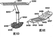
Fig. 8 A shows the structure of the electric device that uses light-emitting device of the present invention to 8E.
Embodiment
Below, with basic structure, operating principle and ad hoc structure example embodiments of the present invention are described.Be noted that it is transparent only needing at least one electrode of light-emitting component in order to extract light.Therefore, not only form transparency electrode and extract the common component structure of light but also in fact can use from the structure that the opposite side of substrate extracts the structure of light and extracts light from the both sides of electrode from substrate at substrate.
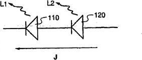
The basic structure of light-emitting component of the present invention at first, is described with reference to Figure 1A.Figure 1A shows the structure example of light-emitting component of the present invention, and wherein first light- emitting component 110 and 120 series connection of second light-emitting component are laminated on the substrate 100.First light-emitting component 110 has luminescent layer 112 between the first anode 111 and first negative electrode 113, and second light-emitting component 120 has luminescent layer 122 between second plate 121 and second negative electrode 123.Each luminescent layer 112 and 122 comprises luminous organic compound.
When the first anode 111 sides of giving light-emitting component apply positive bias, when applying back bias voltage for second negative electrode, 123 sides, the electric current with a certain current density, J flows through this element.Simultaneously, from luminescent layer 112 injected holes of the first anode 111 to first light-emitting components, from the luminescent layer 112 injection electronics of first negative electrode, 113 to first light-emitting components.When hole and electronics again in conjunction with the time, first light 130 can be provided by first light-emitting component 110.From luminescent layer 122 injected holes of second plate 121 to second light-emitting components, from the luminescent layer 122 injection electronics of second negative electrode, 123 to second light-emitting components.When hole and electronics again in conjunction with the time, second light 140 can be provided by second light-emitting component 120.In other words, both can also can provide light by second light-emitting component 120 by first light-emitting component 110.
Be noted that the circuit at light-emitting component shown in Figure 1B.Electric current with common current density, J flows through first light-emitting component 110 and second light-emitting component 120, and wherein luminous the and current density, J of each brightness aspect (L1 among Figure 1B and L2) is corresponding.Simultaneously, in the example shown in Figure 1A, when the first anode 111, first negative electrode 113 and second plate 121 had optical transmission performance, first light 130 and second light 140 can extract.
In the present invention, any in first light 130 and second light 140 shows first emission spectrum with at least two crests.Another shows second emission spectrum that has crest in the position that is different from first emission spectrum.For example, first light 130 shows in indigo plant and have first emission spectrum of crest in the orange wave-length coverage in bluish-green wave-length coverage and at Huang.Second light 140 shows at orange and (describe) second emission spectrum with a crest in detail in red wave-length coverage in following execution mode 1.Be noted that indigo plant has complementary colours with Huang to orange emission look to bluish-green emission look and concerns.
For the emission spectrum with two crests (first emission spectrum in the above-mentioned example) is provided, for coming luminous light-emitting component relatively easy by use electric current stimulated luminescence organic compound, this can be with dual wavelength white light emitting elements of the prior art as representative.Yet, provide the emission spectrum with three or more crest or wide emission spectrum just to be difficult to.Structure of the present invention is the method that solves this technical problem.In other words, this structure is such, resemble the light-emitting component that has the emission spectrum (first emission spectrum in the above-mentioned example) of two crests the dual wavelength white light emitting elements based on demonstration, the light-emitting component that in the scope that only can't compensate with said elements, has an emission spectrum connect lamination and overlapping light.If have only the light-emitting component of single crest to compare with the series connection lamination, use this structure, the quantity of the element of lamination can reduce a lot.Therefore, can suppress the increase of driving voltage.Therefore, this structure is effective.As shown in Figure 1B, in light-emitting component of the present invention, can obtain brightness, this brightness is the summation with respect to the brightness of the brightness of the L1 of a certain current density, J acquisition and L2.Therefore, can also provide high brightness with respect to electric current (in other words, current efficiency).
Be noted that it is that first light-emitting component 110 shows that first emission spectrum and second light-emitting component 120 with at least two crests are presented at the situation that the position that is different from first emission spectrum has second emission spectrum of a crest as mentioned above; Yet this structure also can be conversely.In other words, first emitting element 110 can show second emission spectrum and second light-emitting component 120 can show first emission spectrum.Though Figure 1A shows such structure, wherein provide substrate 100 as the first anode 111 sides, can provide this substrate 100 as second negative electrode, 123 sides.And, though Figure 1A shows such structure, wherein extract light from the first anode 111 sides, also can extract light from second negative electrode, 123 sides shown in Fig. 4 A or from the both sides shown in Fig. 4 B.
Recited above is the situation that each luminescent layer 112 and 122 comprises luminous organic compound, but these luminescent layers can be to comprise luminous organic compound with regard to one.In other words, light- emitting component 110 and 120 can be inorganic light-emitting device (LED).One in first light 130 and second light 140 has shown first emission spectrum with at least two crests, and another has shown second emission spectrum that has crest in the position that is different from first emission spectrum.For example, first light 130 has shown not only in indigo plant to have first emission spectrum of crest in the orange wave-length coverage in bluish-green wave-length coverage but also at Huang, and second light 140 has shown second emission spectrum that has crest at orange in the red wave-length coverage.Be noted that the emission look corresponding with these two crests of first emission spectrum has the complementary color relation.This second emission spectrum also can all have crest in two wave-length coverages with complementary color relation.Under the sort of situation, this second emission spectrum preferably has crest in the position that is different from first emission spectrum.In other words, two emission looks being formed by this first light preferably with two that are formed by second light launch looks different.
Concept of the present invention not only can be applied to the light-emitting component with galvanoluminescence shown in Figure 1A and 1B also can be applied to resemble collision excitation light-emitting component the inorganic EL.
In other words, two collision excitation light-emitting components connection that is one another in series.A demonstration of these two collision excitation light-emitting components has first emission spectrum of at least two crests, and another is presented at second emission spectrum that the position that is different from first emission spectrum has a crest.The emission look corresponding with two crests of first emission spectrum has the complementary color relation.This second emission spectrum also can all have crest in two wave-length coverages with complementary color relation.Under the sort of situation, this second emission spectrum preferably has crest in the position that is different from first emission spectrum.In other words, two kinds of emission looks that preferably are different from the light that sends from the another one light-emitting component from two kinds of emission looks of a light that sends of two collision excitation light-emitting components.
As an example, to orange wave-length coverage the complementary color relation is described to bluish-green wave-length coverage and Huang with blue; Yet, also can use another kind of complementary color relation (for example, bluish-green to green wave-length coverage and orange to red wave-length coverage).Very wide white light (describing in detail) preferably, different complementary color relations is applied to the emission look of first light-emitting component and the emission look of second light-emitting component, because can be provided like this in following execution mode 2.
According to aforesaid structure, can cover most of visible-range, and be easy to provide white light efficiently.Then, below describe than the have superiority structure example of the combination of having considered the emission look of prior art.
[execution mode 1]
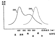
In Fig. 2 A, component structure has been shown.Fig. 2 A shows the structure example of light-emitting component of the present invention, and wherein first light- emitting component 210 and 220 series connection of second light-emitting component are laminated on the substrate 200.This first light-emitting component 210 has luminescent layer 212 between the first anode 211 and first negative electrode 213.This second light-emitting component 220 has luminescent layer 222 between second plate 221 and second negative electrode 223.
Here, the luminescent layer 212 of first light-emitting component comprises the first luminescent layer 212-1 that is presented at the blue emission spectrum that has crest in the bluish-green wave-length coverage and is presented at the second luminescent layer 212-2 that Huang has the emission spectrum of crest in the orange wave-length coverage.The luminescent layer 222 of second light-emitting component shows the emission spectrum that has crest at orange in the red wave-length coverage.The lamination order of the first luminescent layer 212-1 and the second luminescent layer 212-2 can be put upside down.
When the first anode 211 sides of giving light-emitting component apply positive bias, when applying back bias voltage for second negative electrode, 223 sides, can provide first light 230 and second light 240.First light 230 be from the first luminescent layer 212-1 and the second luminescent layer 212-2, send in conjunction with light; Therefore, it shows not only to have the emission spectrum of crest in indigo plant in the orange wave-length coverage in bluish-green wave-length coverage but also at Huang shown in Fig. 2 B.In other words, first emitting element shows dual wavelength white or approximate white (pure look, yellow-white etc.) emission look.Second light 240 is presented at the emission spectrum that orange has crest in the red wave-length coverage shown in Fig. 2 B.
Therefore because first light 230 and second light 240 are overlapping, according to the light-emitting component of the present invention of execution mode 1 can provide cover blue to bluish-green wave-length coverage, yellow light to orange wave-length coverage, orange to red wave-length coverage.
This first light-emitting component 210 has the structure similar with the dual wavelength white light emitting elements that adopts normally used complementary color relation, and can realize having the white or approximate white light-emitting component of high brightness and good component life.Yet this first light-emitting component shows weak spectrum in red wave-length coverage, and is not suitable for using the full-color display of filter.Be appreciated that the structure in the execution mode 1 can address this problem effectively.
Even the brightness of the first luminescent layer 212-1 (showing the emission spectrum that has a crest in indigo plant in the bluish-green wave-length coverage) for example worsens or during with current density change in time, the first luminescent layer 212-1 to the contribution of whole spectrum near 1/3rd.Therefore, this structure has the less relatively advantage of colourity variation.Under the situation that includes only the light-emitting component that resembles first light-emitting component 210 the common dual wavelength white light emitting elements, the brightness of the first luminescent layer 212-1 changes greatly influences colourity.
Can provide and execution mode 1 similar emission spectrum by series connection lamination three light-emitting components: at indigo plant luminous light-emitting component in the bluish-green wave-length coverage, Huang in the orange wave-length coverage luminous light-emitting component and in orange arrives red wave-length coverage luminous light-emitting component.Yet under the sort of situation, driving voltage becomes in the execution mode 1 1.5 times of driving voltage of light-emitting of two elements of series connection lamination or more.
As mentioned above, as an example be because have two luminescent layers (212-1 and 212-2), show that at first light-emitting component 210 first emission spectrum and second light-emitting component 220 with two crests are presented at the situation that the position that is different from first emission spectrum has second emission spectrum of crest.Yet this second light-emitting component 220 can show first emission spectrum.In other words, this second light-emitting component 220 can show owing to having two-layer luminescent layer to have first emission spectrum of two crests, and this first light-emitting component 210 may be displayed on second emission spectrum that the position that is different from first emission spectrum has crest.Though Fig. 2 A shows such structure, wherein provide substrate 200 as the first anode 211 sides, also can provide this substrate as second negative electrode, 223 sides.And, though Fig. 2 A shows such structure, wherein extract light from the first anode 211 sides, also can extract light from second negative electrode, 223 sides or both sides.
[execution mode 2]
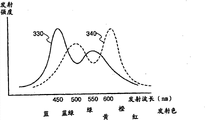
In Fig. 3 A, component structure has been shown.Fig. 3 A shows the structure example of light-emitting component of the present invention, and wherein first light-emitting component 310 and second light-emitting component 320 are at substrate 300 lamination of connecting.This first light-emitting component 310 has luminescent layer 312 between the first anode 311 and first negative electrode 313, this second light-emitting component 320 has luminescent layer 322 between second plate 321 and second negative electrode 323.
Here, the luminescent layer 312 of first light-emitting component comprises the first luminescent layer 312-1 that is presented at the blue emission spectrum that has crest in the bluish-green wave-length coverage and is presented at the second luminescent layer 312-2 that Huang has the emission spectrum of crest in the orange wave-length coverage.The luminescent layer 322 of second light-emitting component comprises the 3rd luminescent layer 322-1 that is presented at the bluish-green emission spectrum that has crest in the green wave-length coverage and has the 4th luminescent layer 322-2 of the emission spectrum of crest in the red scope at orange.The lamination order that is noted that the first luminescent layer 312-1 and the second luminescent layer 312-2 can be put upside down.The lamination order of the 3rd luminescent layer 322-1 and the 4th luminescent layer 322-2 can be put upside down.
When the first anode 311 sides of giving light-emitting component apply positive bias, when applying back bias voltage for second negative electrode, 323 sides, can provide first light 330 and second light 340.First light 330 be from the first luminescent layer 312-1 and the second luminescent layer 312-2, send in conjunction with light; Therefore, it shows not only to have the emission spectrum of crest in indigo plant in the orange wave-length coverage in bluish-green wave-length coverage but also at Huang shown in Fig. 3 B.In other words, first light 330 is that the white or approximate white hair of dual wavelength is penetrated look.Second light 340 be from the 3rd luminescent layer 322-1 and the 4th luminescent layer 322-2, send in conjunction with light; Therefore, it shows not only to have the emission spectrum of crest bluish-green in the red wave-length coverage in green wave-length coverage but also at orange shown in Fig. 3 B.In other words, second light-emitting component 320 shows and has the white or approximate white hair of the dual wavelength that is different from first light-emitting component 310 and penetrate look.
Therefore because first light 330 and second light 340 are overlapping, according to the light-emitting component of the present invention of execution mode 2 can provide cover blue to bluish-green wave-length coverage, bluish-green to green wave-length coverage, yellow light to orange wave-length coverage, orange to red wave-length coverage.
This first light-emitting component 310 and second light-emitting component 320 all have the structure similar with the dual wavelength white light emitting elements that adopts normally used complementary color relation, and can realize having the white or approximate white light-emitting component of high brightness and good component life.Yet this first light-emitting component 310 mainly shows weak spectrum to green wave-length coverage and orange bluish-green in red wave-length coverage, and is not suitable for using the full-color display of filter.In addition, first light-emitting component has narrow spectrum and lacks vividness in emerald green wave-length coverage.Yet, be appreciated that according to the structure of execution mode 2 can remedy this defective with the emission spectrum of second light-emitting component 320 of lamination and can address this problem effectively.
Even the brightness of the first luminescent layer 312-1 (showing the emission spectrum that has crest in indigo plant in the bluish-green wave-length coverage) for example worsens in time or changes when depending on current density, the first luminescent layer 312-1 to the contribution of whole spectrum near 1/4th.Therefore, this structure has the less relatively advantage of colourity variation.Under the situation that includes only the light-emitting component that resembles first light-emitting component 310 the common dual wavelength white light emitting elements, the brightness of the first luminescent layer 312-1 changes greatly influences colourity.
Can provide and execution mode 2 similar emission spectrum by four light-emitting components of series connection lamination: luminous light-emitting component in indigo plant arrives bluish-green wave-length coverage, bluish-green in the green wave-length coverage luminous light-emitting component, at Huang luminous light-emitting component and at orange luminous light-emitting component in the red wave-length coverage in the orange wave-length coverage.Yet under the sort of situation, driving voltage becomes in the execution mode 22 times of driving voltage of light-emitting of two elements of series connection lamination or more.
As mentioned above, as an example be to show not only in indigo plant to bluish-green wave-length coverage but also have the spectrum of crest and 320 demonstrations of second light-emitting component in the orange wave-length coverage at Huang and not only had the situation of the spectrum of crest bluish-green in the red wave-length coverage to green wave-length coverage but also at orange at first light-emitting component 310.Yet they can be put upside down.In other words, this second light-emitting component 320 can show not only have crest to bluish-green wave-length coverage but also at Huang in indigo plant in orange wave-length coverage, and this first light-emitting component 310 both can show to have crest at orange to green wave-length coverage bluish-green in red wave-length coverage.Though Fig. 3 A shows such structure, wherein provide substrate 300 as the first anode 311 sides, also can provide this substrate as second negative electrode, 323 sides.And, though Fig. 3 A shows such structure, wherein extract light from the first anode 311 sides, also can extract light from second negative electrode, 323 sides or both sides.
[execution mode 3]
Below describe the structure of light-emitting component of the present invention, especially, can be used for first light-emitting component 110 of Figure 1A and material and the component structure of second light-emitting component 120.Light-emitting component of the present invention only need have at least a structure shown in Figure 1A.Yet hole injection layer and/or hole transmission layer can be arranged between the first anode 111 of first light-emitting component and the luminescent layer 112 and between the second plate 121 and luminescent layer 122 of second light-emitting component.Electron injecting layer and/or electron transfer layer can be arranged between first negative electrode 113 of first light-emitting component and the luminescent layer 112 and between second negative electrode 123 and luminescent layer 122 of second light-emitting component.
Be noted that hole injection layer has the function of accepting the hole from anode, hole transmission layer has the function of hole transport to luminescent layer.Electron injecting layer has the function of accepting electronics from negative electrode, and electron transfer layer has the function of electric transmission to luminescent layer.
The material that can be used for each layer is described as an example especially.Yet, can be applied to material of the present invention and be not limited thereto.
The hole-injecting material that can be used for hole injection layer, phthalocyanine compound are effectively, but also can use phthalocyanine (to be abbreviated as H
2-Pc), copper phthalocyanine (being abbreviated as Cu-Pc), vanadyl phthalocyanine (being abbreviated as VOPc) etc.And, can use the conducting polymer of chemical doping to quantize compound, the polyethylene dioxythiophene (being abbreviated as PEDOT) of for example using poly styrene sulfonate (being abbreviated as PSS) to mix, polyaniline (being abbreviated as PAni) etc.Also can use for example molybdenum oxide (MoOx) of inorganic semiconductor film, vanadium oxide (VOx) or nickel oxide (NiOx), or inorganic insulation ultrathin membrane aluminium oxide (Al for example
2O
3) also be effective.Also can use the aromatic amides based compound, for example, 4,4 ', 4 " three (N, N-diphenyl-amino)-triphenylamines (being abbreviated as TDATA); 4; 4 ', 4 " three [N-(3-tolyl)-N-phenyl-amino]-triphenylamines (being abbreviated as MTDATA), N, N '-two (3-tolyl)-N, N '-diphenyl-1,1 '-biphenyl-4,4 '-diamines (being abbreviated as TPD), 4,4 '-two [N-(1-naphthyl)-N-phenyl-amino]-biphenyl (are abbreviated as α-NPD) or 4,4 '-two [N-(4-(N, N-two-m-tolyl) amino) phenyl-N-phenylamino] biphenyl (being abbreviated as DNTPD).And aromatic diaminodithiol compound can be with having the material doped of acceptor property.Especially, can use acceptor 2,3,5,6-tetrafluoro generation-7, the VOPc that 7,8,8-four cyano quino, 24 phenyl isocyanate methanes (being abbreviated as F4-TCNQ) mix or the α-NPD that uses acceptor MoOx to mix.
As the hole mobile material that can be used for hole transmission layer, the preferred fragrance amine compound also can use aforesaid TDATA, MTDATA, TPD, α-NPD, DNTPD etc.
Electron transport material as being used for electron transfer layer can use metal complex, and for example three (oxine) aluminium (is abbreviated as Alq
3), three (4-methyl-oxine) aluminium (is abbreviated as Almq
3), two (10-hydrogen-oxygen benzo [h]-oxyquinoline) beryllium (is abbreviated as BeBq
2), two (2-methyl-oxine) (4-phenyl phenol) aluminium (being abbreviated as BAlq), two [2-(2-hydroxyphenyl)-benzene azoles] zinc (is abbreviated as Zn (BOX)
2) or two [2-(2-hydroxyphenyl)-benzothiazole] zinc (be abbreviated as Zn (BTZ)
2).Except the metal complex beyond the region of objective existence can also use for example 2-(4-xenyl)-5-(4-four butylbenzene bases)-1,3 of oxadiazole derivative, and 4-diazole (being abbreviated as PBD) or 1,3-two (5-(p-four butylbenzene bases)-1,3,4-diazole-2 base] benzene (being abbreviated as OXD-7); Triazole derivative is 3-(4-four butylbenzene bases)-4-phenyl-5-(4-diphenyl)-1,2 for example, 4-triazole (being abbreviated as TAZ) or 3-(4-four butylbenzene bases)-4-(4-ethyl group phenyl)-5-(4-diphenyl)-1,2,4-triazole (being abbreviated as p-EtTAZ); Imdazole derivatives for example 2,2 ', 2 " (1,3,5-benzene, three bases) three [1-phenyl-1H-benzimidazole] (being abbreviated as TPBI); Or phenanthrolene derivative for example dark phenanthrolene (being abbreviated as BPhen) or dark 2,2 diquinolines (being abbreviated as BCP).
The electronics injection material of electron injecting layer can be used as, for example Alq of above-mentioned electron transport material can be used
3, Almq
3, BeBq
2, BAlq, Zn (BOX)
2, Zn (BTZ)
2, PBD, OXD-7, TAZ, p-EtTAZ, TPBI, BPhen or BCP.Can select, the ultrathin membrane of insulating material for example, often adopts alkali halide for example LiF or CsF, and alkaline-earth halide is CaF for example
2, alkali metal oxide is Li for example
2O etc.In addition, alkali metal complex is lithium acetylacetonate (being abbreviated as Li (acac)) for example, and oxine-lithium (being abbreviated as Liq) etc. also is effective.The electronics injection material can be with having the material doped of alms giver's performance.Can do the alms giver with alkali metal, alkaline-earth metal, rare earth metal etc.Especially, can use the BCP of alms giver's lithium doping, the Alq of alms giver's lithium doping
3
The structure of the luminescent layer (112 or 122) of first light-emitting component 110 or second light-emitting component 120 then, is described.Here listing can be as the material of luminous organic compound; Yet, the invention is not restricted to these materials.Can use any luminous organic compound.
Can be by using perylene, 2,5,8,11-, four-t-bu thylperylene (being abbreviated as TBP), 9,10-biphenyl anthracene etc. be as parasitic material, and by this parasitic material is distributed to obtain in the suitable host material blue to blue green light.Can select, by styryl arylene derivative for example 4,4 '-two (2,2-distyrene base) biphenyl (being abbreviated as DPVBi) or anthracene derivant for example 9,10-two-naphthyl anthracene (being abbreviated as DNA) or 9,10-two (2-naphthyl)-2-t-butyl anthracene (being abbreviated as t-BuDNA) can obtain this light.Can select, also can use polymer for example poly-(9,9-dioctyl fluorene).
Can be by using cumarin primary colours element for example cumarin 30 or coumarin 6, two [2-(2,4-difluorophenyl) pyrimidine] picolinato iridium (being abbreviated as FIrpic), two (2-phenyl pyrimidine) acethylacetonato iridium (is abbreviated as Ir (ppy)
2Etc. (acac)) as parasitic material, and with this parasitic material be distributed to obtain in the suitable host material bluish-green to green glow.Can provide light by above-mentioned perylene or TBP being distributed in the suitable host material with 5wt% or more high concentration.Can select, can be with metal complex for example BAlq, Zn (BTZ)
2, two (2-methyl-oxine) gallium chloride (Ga (mq)
2Cl) provide this light.Also can use polymer for example poly-(p-phenylene 1,2-ethenylidene).
Can be by using rubrene, 4-(dicyano methylene)-2-[p-(dimethylamino) styryl]-6-methyl-4H-pyrans (being abbreviated as DCM1), 4-(dicyano methylene)-2-methyl-6-(9-julolidine) acetenyl-4H-pyrans (being abbreviated as DCM2), two (2-(2-thienyl)) pyrimidine acetylacetonato iridium (is abbreviated as Ir (thp)
2(acac)), two (2-phenylchinoline) acetylacetonato iridium (is abbreviated as Ir (pq)
2Etc. (acac)) as parasitic material, and with this parasitic material be distributed to obtain in the suitable host material yellow to orange light.Also can by metal complex for example two (oxine) zinc (be abbreviated as Znq
2) or two [2-cinnamoyl-oxine] zinc (be abbreviated as Znsq
2) light is provided.Also can use polymer for example poly-(2,5-dialkoxy-1,4-phenylene 1,2-ethenylidene).
Can be by using 4-(dicyano methylene)-2,6-two [p-(dimethylamino) styryl]-4H-pyrans (being abbreviated as BisDCM), 4-(dicyano methylene)-2,6-two [2-(julolidine-9-yl) acetenyl]-4H-pyrans (being abbreviated as DCM1), 4-(dicyano methylene)-2 methyl-6-(9-julolidine) acetenyl]-4H-pyrans (being abbreviated as DCM2), two [2-(2-thienyl) pyrimidine acetylacetonato iridium (is abbreviated as Ir (thp)
2Etc. (acac)) be distributed to as parasitic material, and with this parasitic material and obtain orange in the suitable host material to ruddiness.Also can by metal complex for example two (oxine) zinc (be abbreviated as Znq
2) or two [2-cinnamoyl-oxine] zinc (be abbreviated as Znsq
2) light is provided.Also can use polymer for example poly-(3-alkylthrophene).
Be noted that in said structure suitable host material only need have the emission look shorter or bigger than the energy gap of luminous organic compound than the wavelength of luminous organic compound.Especially, this suitable host material can be selected from the hole mobile material described in the above-mentioned example or electron transport material.Can select, also can use 4,4 '-two (N-carbazyl) biphenyl (being abbreviated as CBP), 4,4 ', 4 " three (N-carbazyl) triphenylamines (being abbreviated as TCTA), 1,3,5-three [(4-(N-carbazyl) phenyl] benzene (being abbreviated as TCPB) etc.
In light-emitting component of the present invention, preferably has the electric conducting material of high work content as anode (first anode 111 and second plate 121) material.Extracting by the first anode 111 under the situation of light, can with transparent conductive material for example tin indium oxide (ITO), indium zinc oxide (IZO), zinc oxide (ZnO) or with silica-doped tin indium oxide for the first anode 111.The first anode 111 sides are being used for protecting under the situation of light, can be with the monofilm of TiN, ZrN, Ti, W, Ni, Pt, Cr etc.; The laminated film of titanium nitride film and comprise the film that Main Ingredients and Appearance is aluminium; The three-decker of titanium nitride film comprises the film that Main Ingredients and Appearance is aluminium, and another layer titanium nitride film etc. is used for the first anode 111.Can select, can press by the reflecting electrode upper strata at Ti, Al etc. and state transparent conductive material and form the first anode 111.Second plate 121 needs the transmission light, and it can use transparent conductive material for example outside ITO, IZO or the ZnO, can also use the above-mentioned hole transport compound (especially, aromatic amine based compound) that is doped with the material with acceptor performance to form.Especially, can be with acceptor 2,3,5, the 6-tetrafluoro is for-7, and 7,8,8-four cyano quino, 24 phenyl isocyanate methanes (are abbreviated as F
4-the VOPc that TCNQ) mixes or the α-NPD that uses acceptor MoOx to mix are used for second plate 121.
As negative electrode (first negative electrode 113 and second negative electrode 123) material, the preferred electric conducting material with low work content that uses.Especially, except can using alkali metal for example Li or Cs, alkaline-earth metal is Mg, Ca or Sr or comprise outside the alloy of metal (Mg:Ag, Al:Li etc.) for example, and for example Yb or Er form negative electrode can also to use rare earth metal.Using LiF, CsF, CaF
2, Li
2Under the situation of the electron injecting layer of O etc., can use the conductive film of typical aluminium etc.Extracting under the situation of light by second negative electrode 123, can use to comprise for example for example Mg, Ca or the ultrathin membrane of Sr and the laminar structure of nesa coating (ITO, IZO or ZnO etc.) of Li or Cs and alkaline-earth metal of alkali metal.Can select, above-mentioned electron transport material can mix with the material with alms giver's performance (alkali metal, alkaline-earth metal etc.), and nesa coating (ITO, IZO or ZnO etc.) lamination in the above.First negative electrode 113 needs transmission light, and above-mentioned electron transport material can mix with the material with alms giver's performance (alkali metal, alkaline-earth metal etc.).Especially, can use by the BCP of alms giver's lithium doping or by the Alq of alms giver's lithium doping
3
The method that is noted that each luminescent layer of lamination is not confined to make above-mentioned light-emitting component of the present invention especially.Have only and to carry out lamination, can select either party's rule such as vacuum vapor deposition method, spin-coating method, ink-jet method or dip coating.
[embodiment]
Embodiments of the invention are below described.
[embodiment 1]
With reference to figure 5, describe the manufacture method of component structure of the present invention and light-emitting component in an embodiment in detail.
It is the substrate of glass 500 of tin indium oxide (ITO) film of 110nm that preparation provides thickness.This ITO film that provides is used as the first anode 511 in the present embodiment.
The substrate of glass 500 that provides the first anode 511 is installed in and makes the surface that provided by the first anode 511 down on the substrate frame in the vacuum evaporator.Then, adopt vacuum vapor deposition method to form the thick CuPc film of 20nm to form hole injection layer 512 at the first anode 511.By being provided in the evaporation source that provides at vacuum evaporator, method cutting CuPc carries out vacuum evaporation.Be noted that hole injection layer 512 is also as hole transmission layer in the present embodiment.
The luminescent layer 513 of first light-emitting component 510 is formed on the hole injection layer 512.In the present embodiment, the luminescent layer 513 of first light-emitting component 510 comprises the first luminescent layer 513-1 and the second luminescent layer 513-2.The first luminescent layer 513-1 contacts with the second luminescent layer 513-2.
The first luminescent layer 513-1 comprises α-NPD and perylene, and forms by coevaporation method as evaporation source with α-NPD and perylene.Simultaneously, adjust and make the perylene that in α-NPD, comprises 3 quality %.Thickness is 30nm.In the first luminescent layer 513-1, perylene is as the blue luminous organic compound to blue green light of emission.
The second luminescent layer 513-2 comprises DNA and DCM2, and forms by coevaporation method as evaporation source with DNA and DCM2.Simultaneously, adjust and make the DCM2 that in DNA, comprises 0.1 quality %.Thickness is 30nm.In the second luminescent layer 513-2, DCM2 is as the luminous organic compound that emits yellow to orange light.
Then, forming thickness at the luminescent layer 513 of first light-emitting component 510 is that the BCP film of 10nm is to form electron transfer layer 514.Then, forming thickness at electron transfer layer 514 is the Alq of 20nm
3Film is to form electron injecting layer 515.Under the situation that forms hole injection layer 512, these layers also form by vacuum vapor deposition method.
And, form first negative electrode 516 at electron injecting layer 515.First negative electrode 516 comprises electric transmission compd B CP and for BCP provides the material lithium of alms giver's performance, and forms by coevaporation method as evaporation source with BCP and lithium.Simultaneously, adjust and make the lithium that in BCP, comprises 0.5 quality %.Thickness is 10nm.
After forming first light-emitting component 510 in this way, series connection lamination second light-emitting component 520.Second plate 521 is that the MoOx film of 10nm forms by forming thickness.Under the situation that forms hole injection layer 512, also form second plate 521 by vacuum vapor deposition method.
Then, forming thickness at second plate 521 is that α-NPD film of 50nm is to form hole injection layer 522.Be noted that in the present embodiment hole injection layer 522 is also as hole transmission layer.Under the situation that forms hole injection layer 512, also form hole injection layer 522 by vacuum vapor deposition method.
The luminescent layer 523 of second light-emitting component is formed on the hole injection layer 522.The luminescent layer 523 of second light-emitting component comprises CBP and Ir (btp)
2(acac), and with CBP and Ir (btp)
2(acac) form by coevaporation method as evaporation source.Simultaneously, adjust and make the Ir (btp) that in CBP, comprises 8 quality %
2(acac).Thickness is 30nm.In the luminescent layer 523 of second light-emitting component, Ir (btp)
2(acac) as the luminous organic compound of launching the color that is different from first light-emitting component.
Forming thickness at the luminescent layer 523 of second light-emitting component is that the BCP film of 10nm is to form electron transfer layer 524.Forming thickness at electron transfer layer 524 is the Alq of 20nm
3Film is to form electron injecting layer 525.Under the situation that forms hole injection layer 512, these layers also form by vacuum vapor deposition method.
Form second negative electrode 526 at electron injecting layer 525.Second negative electrode 526 comprises electric transmission compd B CP and for BCP provides the material lithium of alms giver's performance, and forms by coevaporation method as evaporation source with BCP and lithium.Simultaneously, adjust and make the lithium that in BCP, comprises 0.5 quality %.Thickness is 10nm.Second negative electrode 526 also is the Al formation of 150nm by evaporation thickness.
Since first light-emitting component 510 that forms as mentioned above have emission blue to blue green light first luminescent layer and emit yellow to second luminescent layer of orange light, it is presented at the blue emission spectrum that has two crests in to bluish-green wave-length coverage and Huang to orange wave-length coverage.Because second light-emitting component, 520 red-emittings, it is presented at the emission spectrum that the position that is different from first light-emitting component has a crest.
Therefore, the light-emitting component of present embodiment, wherein first light-emitting component 510 and second light-emitting component 520 series connection laminations, by between the first anode 511 and second negative electrode 526, applying voltage, can provide the extensive blue wide white light that arrives orange wave-length coverage and red wave-length coverage to bluish-green wave-length coverage, Huang that covers.Even worsen in time or during with current density change, because the wide spectrum effect, the change of colourity is less relatively in the brightness of arbitrary look of three coloured light.
[embodiment 2]
With reference to figure 6, describe the manufacture method of component structure of the present invention and light-emitting component in an embodiment in detail.
It is the substrate of glass 600 of tin indium oxide (ITO) film of 110nm that preparation provides thickness.This ITO film that provides is used as the first anode 611 in the present embodiment.
The substrate of glass 600 that provides the first anode 611 is installed in and makes the surface that provided by the first anode 611 down on the substrate frame in the vacuum evaporator.Then, adopt vacuum vapor deposition method to form the thick DNTPD film of 20nm to form hole injection layer 612 at the first anode 611.Evaporate DNTPD by cutting DNTPD in the evaporation source that provides at vacuum evaporator and the method that is heated by resistive and carry out vacuum evaporation.
Then, forming thickness at hole injection layer 612 is that α-NPD film of 20nm is to form hole transmission layer 613.Under the situation that forms hole injection layer 612, also form hole transmission layer 613 by vacuum vapor deposition method.
The luminescent layer 614 of first light-emitting component is formed on the hole transmission layer 613.In the present embodiment, the luminescent layer 614 of first light-emitting component comprises the first luminescent layer 614-1 and the second luminescent layer 614-2.The first luminescent layer 614-1 contacts with the second luminescent layer 614-2.
The first luminescent layer 614-1 comprises α-NPD and TBP, and forms by coevaporation method as evaporation source with α-NPD and TBP.Simultaneously, adjust and make the TBP that in α-NPD, comprises 1 quality %.Thickness is 10nm.In the first luminescent layer 614-1, TBP is as the blue luminous organic compound to blue green light of emission.
The second luminescent layer 614-2 comprises α-NPD and DCM2, and forms by coevaporation method as evaporation source with α-NPD and DCM2.Simultaneously, adjust and make the DCM2 that in α-NPD, comprises 1 quality %.Thickness is 10nm.In the second luminescent layer 614-2, DCM2 is as the luminous organic compound that emits yellow to orange light.
Then, forming thickness at the luminescent layer 614 of first luminescent layer is that the BAlq film of 20nm is to form electron transfer layer 615.Then, forming thickness at electron transfer layer 615 is the Alq of 30nm
3Film is to form electron injecting layer 616.Under the situation that forms hole injection layer 612, these layers also form by vacuum vapor deposition method.
And, form first negative electrode 617 at electron injecting layer 616.First negative electrode 617 comprises electric transmission compd B CP and for BCP provides the material lithium of alms giver's performance, and forms by coevaporation method as evaporation source with BCP and lithium.Simultaneously, adjust and make the lithium that in BCP, comprises 0.5 quality %.Thickness is 10nm.
After forming first light-emitting component 610 in this way, series connection lamination second light-emitting component 620.Second plate 621 comprises hole transport compound α-NPD and for α-NPD provides the material MoOx of alms giver's performance, and forms by coevaporation method as evaporation source with α-NPD and MoOx.Simultaneously, adjust and make the MoOx that in α-NPD, comprises 25 quality %.Thickness is 50nm.
Then, forming thickness at second plate 621 is that α-NPD film of 25nm is to form hole injection layer 622.Under the situation that forms hole injection layer 612, hole injection layer 622 also forms by vacuum vapor deposition method.Be noted that in the present embodiment hole injection layer 622 is also as hole transmission layer.
The luminescent layer 623 of second light-emitting component is formed on the hole injection layer 622.In the present embodiment, the luminescent layer 623 of second light-emitting component comprises the 3rd luminescent layer 623-1 and the 4th luminescent layer 623-2.The 3rd luminescent layer 623-1 contacts with the 4th luminescent layer 623-2.
The 3rd luminescent layer 623-1 comprises α-NPD and BisDCM, and forms by coevaporation method as evaporation source with α-NPD and BisDCM.Simultaneously, adjust and make the BisDCM that in α-NPD, comprises 2 quality %.Thickness is 15nm.In the 3rd luminescent layer 623-1, BisDCM is as the luminous organic compound of emission orange to red (especially red) light.
Be the Ga (mq) of 20nm by forming thickness
2The Cl film forms the 4th luminescent layer 623-2.Under the situation that forms hole injection layer 622, the 4th luminescent layer 623-2 also forms by vacuum vapor deposition method.In the 4th luminescent layer 623-2, Ga (mq)
2Cl is as the bluish-green luminous organic compound to green (especially emerald green) light of emission.
Form second negative electrode 625 at electron injecting layer 624.Second negative electrode 625 comprises electric transmission compd B CP and for BCP provides the material lithium of alms giver's performance, and forms by coevaporation method as evaporation source with BCP and lithium.Simultaneously, adjust and make the lithium that in BCP, comprises 0.5 quality %.Thickness is 10nm.Second negative electrode 625 also is the Al formation of 150nm by evaporation thickness.
Since first light-emitting component 610 that forms as mentioned above have emission blue to blue green light first luminescent layer and emit yellow to second luminescent layer of orange light, it is presented at the blue emission spectrum that has two crests in to bluish-green wave-length coverage and Huang to orange wave-length coverage.Since second light-emitting component 620 have emission bluish-green to green glow the 3rd luminescent layer and the emission orange to the 4th luminescent layer of ruddiness, its be presented at penetrate bluish-green to green wave-length coverage and the orange emission spectrum that has two crests in the red wave-length coverage.
Therefore, the light-emitting component of present embodiment, wherein first light-emitting component 610 and second light-emitting component 620 series connection laminations, by between the first anode 611 and second negative electrode 625, applying voltage, can provide cover blue to bluish-green wave-length coverage, yellow to orange wave-length coverage, bluish-green to green wave-length coverage and orange to red wave-length coverage, i.e. the wide white light of whole visible-range almost.Especially, huge advantage is to realize enough brightness in the emerald green and red wave-length coverage of the enough brightness of only using first light-emitting component can't obtain with white.Even worsen in time or during with current density change, because the wide spectrum effect, the change of colourity is less relatively in the brightness of arbitrary look of four coloured light.
[embodiment 3]
In the present embodiment, with reference to figure 7A and 7B the light-emitting device with light-emitting component of the present invention is described.Be noted that Fig. 7 A is the top view of light-emitting device, Fig. 7 B is the cross-sectional view from line A-A ' intercepting.The Reference numeral 701 expression driving circuit section (source drive circuit) that are shown in broken lines; 702, pixel parts and 703, driving circuit section (gate side driver circuit).Reference numeral 704 expression hermetic sealing substrates; 705, sealant and 707 is by the space of sealant 705 encirclements.
Reference numeral 708 expression is used for transmitting the distribution of the signal that will be input to source drive circuit 701 and gate side driver circuit 703 and is used for receiving vision signal from external input terminals FPC (flexible print circuit) 709, clock signal, initial signal, reset signal etc.Be noted that FPC only is shown here; Yet, also can provide FPC with printed substrate (PWB).Light-emitting device in this specification comprises that not only light-emitting device itself also comprises the light-emitting device with FPC or PWB.
Then, with reference to figure 7B cross-sectional structure is described.Driving circuit section and pixel parts are formed on the device substrate 710.Here, show source drive circuit 701 and pixel parts 702 as driving circuit section.
Be noted that the cmos circuit in conjunction with n-passage TFT 723 and p-passage TFT 724 forms source drive circuit 701.The circuit that forms drive circuit can form with the cmos circuit of knowing, PMOS circuit or nmos circuit.Describe to drive integrated pattern in the present embodiment, drive at this that drive circuit is formed on sound (sane) substrate in integrated pattern, but this is not exclusive that drive circuit can be formed on the outside of substrate.
Pixel parts 702 has a plurality of pixels, and each pixel comprises the anode 713 that switches TFT 711, Current Control TFT 712 and be electrically connected to the grounded part of Current Control TFT 712.Be noted that and form insulator 714 to cover an end of anode 713.Here, positive type photosensitive acrylic resin film is used as insulator 714.
Be the coverage rate of the film that improve to form, form in the top or the lower end has the insulator 714 of curved surface.For example, using under the situation of positive type photosensitive acrylic resin as insulator 714 materials, be preferably formed the insulator 714 of the curved surface that only has radius of curvature (0.2 μ m is to 3 μ m) in the upper end.Also can use by light in etchant, become undissolved negative type or by light in etchant, become the dissolving positive type as insulator 714.Not only for example silicon dioxide or silicon oxynitride also can use for organic compound but also inorganic compound.
Light-emitting component 715 and negative electrode 716 can be formed on the anode 713.Here, the preferred use has the material of high work content as the material of anode 713.For example, anode 713 can be by using monofilm for example ITO (tin indium oxide) film, ITSO (silicon dioxide indium tin) film, IZO (indium zinc oxide) film, titanium nitride film, chromium film, tungsten film, Zn film or Pt film; Titanium nitride film and comprise the laminate layers that Main Ingredients and Appearance is the film of aluminium; Or titanium nitride film, the three-decker that comprises film that Main Ingredients and Appearance is aluminium and another layer titanium nitride film form.By the ITO film and be connected to anode 713 that the distribution of the Current Control TFT 712 of anode 713 forms have titanium nitride film and comprise laminate layers structure or titanium nitride film that Main Ingredients and Appearance is the film of aluminium, when comprising the three-decker of film that Main Ingredients and Appearance is aluminium and another layer titanium nitride film, because distribution and with the good Ohmic contact of ITO film, this distribution can have low impedance.And, can be with anode 713 as anode.Anode 713 can by with light-emitting component 715 of the present invention in first anode identical materials form.Can select, anode 713 can form with the first anode of light-emitting component 715 is whole.
Light-emitting component 715 of the present invention has first light-emitting component 110 shown in Figure 1A and the 1B and the laminar structure of second light-emitting component 120.Especially, light-emitting component 715 has the structure similar to execution mode, embodiment 1 and embodiment 2.
Negative electrode 716 can (Al, Ag, Li, Ca or its alloy be MgAg, MgIn, AlLi, CaF for example by the material with low work content
2Or CaN) forms; Yet, it is not particularly limited.By selecting suitable electronics injection material, can use various conducting films.Under the situation of the light that sends from light-emitting component 715 of the present invention by negative electrode 716 transmission, can imagine that negative electrode 716 is by passing through the thin metallic film of laminate thickness and ITO (tin indium oxide), ITSO (silicon dioxide indium tin), indium oxide-tin oxide (In
2O
3-ZnO), zinc oxide nesa coatings such as (ZnO) forms.Negative electrode 716 can by with light-emitting component 715 of the present invention in the second negative electrode identical materials form.Can select, negative electrode 716 can form with second negative electrode of light-emitting component 715 is whole.
By hermetic sealing substrate 704 usefulness sealants 705 are attached to device substrate 710, in the space 707 that is surrounded by device substrate 710, hermetic sealing substrate 704 and sealant 705, provide light-emitting component 715.Be noted that space 707 can also can fill up with inert gas (nitrogen, argon etc.) with sealant 705.
Be noted that preferred use epoxy is as sealant 705.This material preferably makes the least possible moisture and oxygen permeate.As hermetic sealing substrate 704, except glass substrate or quartz base plate, can also use the plastic base by FRP (fiberglass reinforced plastics), PVF (polyvinyl fluoride), wheat are drawn, polyester, acrylic acid etc. form.
As mentioned above, can provide the light-emitting device with light-emitting component of the present invention.
Be noted that described light-emitting device can very freely be combined with the structure of the light-emitting component described in execution mode, embodiment 1 and the embodiment 2 in the present invention.And, if desired, use for example filter of chroma conversion film in the present embodiment in the described light-emitting device.
[embodiment 4]
To 8E, the various electronic installations that the light-emitting component of the application of the invention is finished are described in the present embodiment with reference to figure 8A.
The example that use has the electronic installation that the light-emitting device of light-emitting component of the present invention makes can provide as follows: television set, camera is video camera and digital camera for example, goggle-type display (heat is installed display), navigation system, automatic replay device (automobile audio, audio-frequency assembly etc.), PC, game machine, personal digital assistant (PDA) (mobile computer, cellular phone, portable game machine, e-book etc.), comprise recording medium (especially, the device that can heavily visit recording medium for example Digital video disc (DVD) and have the display that can show image) image playback apparatus, lighting device etc.Show the embodiment of these electronic installations to 8E at Fig. 8 A.
Fig. 8 A shows display, and it comprises chassis 8001, support section 8002, display part 8003, speaker portion 8004, video output terminals 8005 etc.As display part 8003, this display is made by using light-emitting device formed according to the present invention.This display comprises for demonstration information, comprises all displays of PC, TV broadcast reception, advertisement etc.
Fig. 8 B shows pocket pc, and it comprises main body 8101, chassis 8102, display part 8103, keyboard 8104, outer connection part 8105, indication mouse 8106 etc.This pocket pc is as display part 8103, and the light-emitting device that has light-emitting component of the present invention by use is made.
Fig. 8 C shows video camera, and it comprises main body 8201, display part 8202, chassis 8203, outer connection part 8204, shakes control receiving unit 8205, image receiving unit 8206, battery 8207, video importation 8208, operation keys 8209, eyepiece part 8210 etc.This video camera is as display part 8202, and the light-emitting device that has light-emitting component of the present invention by use is made.
Fig. 8 D shows desk lamp device, and it comprises luminous component 8301, cover 8302, adjustable arm 8303, support bar 8304, base 8305, mains switch 8306.This desk lamp device is as luminous component 8301, and the light-emitting device that has light-emitting component of the present invention by use is made.Be noted that this lighting device comprises the lighting device that maximum limit is fixing, wall-mounted lighting device etc.
Fig. 8 E shows cellular phone, and it comprises, and main body 8401, chassis 8402, display part 8403, audio frequency importation 8404, audio output part divide 8405, operation keys 8406, outer connection part 8407, antenna 8408 etc.This cellular phone is as display part 8403, and the light-emitting device that has light-emitting component of the present invention by use is made.
As mentioned above, can provide electronic installation or the lighting device that uses light-emitting component of the present invention.The range of application of light-emitting device with light-emitting component of the present invention is wide especially, and this light-emitting device can be used for the electronic installation of all spectra.
Reference numeral 100: substrate, 110: the first light-emitting components, 111: the first anode, 112: luminescent layer, 113: the first negative electrodes, 120: the second light-emitting components, 121: second plate, 122: luminescent layer, 123: the second negative electrodes, 130: the first light, 140: the second light, 200: substrate, 210: the first light-emitting components, 211: the first anode, 212: luminescent layer, 212-1: first luminescent layer, 212-2: second luminescent layer, 213: the first negative electrodes, 220: the second light-emitting components, 221: second plate, 222: luminescent layer, 223: the second negative electrodes, 230: the first light, 240: the second light, 300: substrate, 310: the first light-emitting components, 311: the first anode, 312: luminescent layer, 312-1: first luminescent layer, 312-2: second luminescent layer, 313: the first negative electrodes, 320: the second light-emitting components, 321: second plate, 322: luminescent layer, 322-1: the 3rd luminescent layer, 322-2: the 4th luminescent layer, 323: the second negative electrodes, 330: the first light, 340: the second light, 500: substrate, 510: the first light-emitting components, 511: the first anode, 512: hole injection layer, 513: luminescent layer, 513-1: first luminescent layer, 513-2: second luminescent layer, 514: electron transfer layer, 515: electron injecting layer, 516: the first negative electrodes, 520: the second light-emitting components, 524: electron transfer layer, 525: electron injecting layer, 526: the second negative electrodes, 600: glass substrate, 610: the first light-emitting components, 611: the first anode, 612: hole injection layer, 613: hole transmission layer, 614: luminescent layer, 614-1: first luminescent layer, 614-2: second luminescent layer, 615: electron transfer layer, 616: electron injecting layer, 617: the first negative electrodes, 620: the second light-emitting components, 621: second plate, 622: hole injection layer, 623: luminescent layer, 623-1: the 3rd luminescent layer, 623-2: the 4th luminescent layer, 624: electron injecting layer, 625: the second negative electrodes, 701: the source drive circuit, 702: pixel parts, 703: gate side driver circuit, 704: hermetic sealing substrate, 705: sealant, 707: space, 709:FPC (flexible print circuit), 710: device substrate, 711: switch TFT, 712: Current Control TFT, 713: anode, 714: insulator, 715: light-emitting component, 716: negative electrode, 723:N-passage TFT, 724:P-passage TFT, 8001: the chassis, 8002: support section, 8003: display part, 8004: speaker portion, 8005: video inputs, 8101: main body, 8102: chassis, 8103: the display part, 8104: keyboard, 8105: outer connection part, 8201: theme, 8202: the display part, 8203: the chassis, 8204: outer connection part, 8205: shake the control receiving unit, 8206: the image receiving unit, 8207: battery, 8208: audio frequency importation, 8209: operation keys, 8301: luminous component, 8302: cover, 8303: adjustable arm, 8304: support bar, 8305: base, 8306: mains switch, 8401: main body, 8402: chassis, 8403: the display part, 8404: the audio frequency importation, 8405: audio output part branch, 8406: operation keys, 8407: outer connection part and 8408: antenna.
Claims (28)
1. light-emitting device, it comprises:
Thin-film transistor on substrate, this thin-film transistor comprises:
Semiconductor film on substrate;
The dielectric film adjacent with semiconductor film; With
The gate electrode adjacent with semiconductor film, wherein said dielectric film are arranged between gate electrode and the semiconductor film;
First light-emitting component, this first light-emitting component has first luminescent layer that comprises luminous organic compound between the first anode and first negative electrode;
Second light-emitting component, this second light-emitting component has second luminescent layer that comprises luminous organic compound between second plate and second negative electrode; With
Filter,
Wherein, first light-emitting component and second light-emitting component are connected in series, and are electrically connected with described thin-film transistor,
Wherein, first light-emitting component shows first emission spectrum with at least two crests, and second light-emitting component is presented at second emission spectrum that the position that is different from these two crests has crest,
Wherein, white hair is penetrated look and is shown by first emission spectrum and second emission spectrum, and
Wherein, described filter is set and changes the colourity that this white hair is penetrated look.
2. according to the light-emitting device of claim 1, wherein second emission spectrum has at least two crests.
3. light-emitting device, it comprises:
Thin-film transistor on substrate, this thin-film transistor comprises:
Semiconductor film on substrate;
The dielectric film adjacent with semiconductor film; With
The gate electrode adjacent with semiconductor film, wherein said dielectric film are arranged between gate electrode and the semiconductor film;
First light-emitting component, this first light-emitting component has first luminescent layer that comprises luminous organic compound between the first anode and first negative electrode;
Second light-emitting component, this second light-emitting component has second luminescent layer that comprises luminous organic compound between second plate and second negative electrode; With
Filter,
Wherein, first light-emitting component and second light-emitting component are connected in series, and are electrically connected with described thin-film transistor,
Wherein, first light-emitting component shows the first emission look that comprises two kinds of emission looks with complementary colours relation, and second light-emitting component shows the second emission look that is different from these two kinds emission looks,
Wherein, white hair is penetrated look and is shown by the first emission look and the second emission look, and
Wherein, described filter is set and changes the colourity that this white hair is penetrated look.
4. according to the light-emitting device of claim 3, wherein the second emission look comprises two kinds of emission looks with complementary colours relation, and these two kinds emission looks of the second emission look are different from two kinds of emission looks of the first emission look.
5. light-emitting device, it comprises:
Thin-film transistor on substrate, this thin-film transistor comprises:
Semiconductor film on substrate;
The dielectric film adjacent with semiconductor film; With
The gate electrode adjacent with semiconductor film, wherein said dielectric film are arranged between gate electrode and the semiconductor film;
First light-emitting component, this first light-emitting component has first luminescent layer that comprises luminous organic compound between the first anode and first negative electrode;
Second light-emitting component, this second light-emitting component has second luminescent layer that comprises luminous organic compound between second plate and second negative electrode; With
Filter,
Wherein, first light-emitting component and second light-emitting component are connected in series, and are electrically connected with described thin-film transistor,
Wherein, first light-emitting component is presented at blue interior and have first emission spectrum of crest in the orange wave-length coverage at Huang to bluish-green wave-length coverage, and second light-emitting component is presented at second emission spectrum that the position that is different from these crests has crest,
Wherein, white hair is penetrated look and is shown by first emission spectrum and second emission spectrum, and
Wherein, described filter is set and changes the colourity that this white hair is penetrated look.
6. according to the light-emitting device of claim 5, wherein second emission spectrum is to have the emission spectrum of crest bluish-green in the red wave-length coverage in green wave-length coverage and at orange.
7. light-emitting device, it comprises:
Thin-film transistor on substrate, this thin-film transistor comprises:
Semiconductor film on substrate;
The dielectric film adjacent with semiconductor film; With
The gate electrode adjacent with semiconductor film, wherein said dielectric film are arranged between gate electrode and the semiconductor film;
First light-emitting component, this first light-emitting component has first luminescent layer that comprises luminous organic compound between the first anode and first negative electrode;
Second light-emitting component, this second light-emitting component has second luminescent layer that comprises luminous organic compound between second plate and second negative electrode; With
Filter,
Wherein, first light-emitting component and second light-emitting component are connected in series, and are electrically connected with described thin-film transistor,
Wherein, first light-emitting component is presented in 430nm~480nm wave-length coverage and has first emission spectrum of crest in 550nm~600nm wave-length coverage, and second light-emitting component is presented at second emission spectrum that the position that is different from described crest has crest,
Wherein, white hair is penetrated look and is shown by first emission spectrum and second emission spectrum, and
Wherein, described filter is set and changes the colourity that this white hair is penetrated look.
8. according to the light-emitting device of claim 7, wherein second emission spectrum is in 480nm~550nm wave-length coverage and has the emission spectrum of crest in 600nm~680nm wave-length coverage.
9. according to claim 1,3,5 and 7 any one light-emitting devices, wherein first luminescent layer comprises the 3rd luminescent layer and the 4th luminescent layer that shows the emission look different with the emission look of the 3rd luminescent layer.
10. according to the light-emitting device of claim 9, wherein the 3rd luminescent layer contacts with the 4th luminescent layer.
11. according to claim 1,3,5 and 7 any one light-emitting devices, wherein second luminescent layer comprises the 5th luminescent layer and the 6th luminescent layer that shows the emission look different with the emission look of the 5th luminescent layer.
12. according to the light-emitting device of claim 11, wherein the 5th luminescent layer contacts with the 6th luminescent layer.
13. according to claim 1,3,5 and 7 any one light-emitting devices, wherein second plate comprises hole transport compound and MoOx.
14. according to claim 1,3,5 and 7 any one light-emitting devices, wherein second plate comprises compound and the MoOx based on arylamine.
15. according to claim 1,3,5 and 7 any one light-emitting devices, wherein first negative electrode comprises electron transport material and the material that this electron transport material is had alms giver's character.
16. according to claim 1,3,5 and 7 any one light-emitting devices, wherein first negative electrode comprise electron transport material and to this electron transport material have the material of alms giver's character and wherein this material with alms giver's character be selected from alkali metal and alkaline-earth metal.
17. lighting device, it comprises:
First light-emitting component, this first light-emitting component has first luminescent layer that comprises luminous organic compound between the first anode and first negative electrode;
Second light-emitting component, this second light-emitting component has second luminescent layer that comprises luminous organic compound between second plate and second negative electrode;
Wherein first light-emitting component and second light-emitting component are connected in series,
Wherein first luminescent layer and second luminescent layer overlap each other,
Wherein first luminescent layer comprises the 3rd luminescent layer and the 4th luminescent layer that shows the emission look different with the emission look of the 3rd luminescent layer,
Wherein second luminescent layer comprise the 5th luminescent layer and the 6th luminescent layer and
Wherein first light-emitting component shows first emission spectrum with at least two crests, and second light-emitting component is presented at second emission spectrum that the position that is different from these two crests has crest.
18. according to the lighting device of claim 17, wherein the 3rd luminescent layer contacts with the 4th luminescent layer.
19. according to the lighting device of claim 17, wherein the 6th luminescent layer shows the emission look different with the emission look of the 5th luminescent layer.
20. according to the lighting device of claim 19, wherein the 5th luminescent layer contacts with the 6th luminescent layer.
21. lighting device, it comprises:
First light-emitting component, this first light-emitting component has first luminescent layer that comprises luminous organic compound between the first anode and first negative electrode; With
Second light-emitting component, this second light-emitting component has second luminescent layer that comprises luminous organic compound between second plate and second negative electrode,
Wherein first light-emitting component and second light-emitting component are connected in series,
Wherein first luminescent layer and second luminescent layer overlap each other,
Wherein first luminescent layer comprise the 3rd luminescent layer and the 4th luminescent layer and
Wherein second luminescent layer comprise the 5th luminescent layer and the 6th luminescent layer that shows the emission look different with the emission look of the 5th luminescent layer and
Wherein first light-emitting component shows first emission spectrum with at least two crests, and second light-emitting component is presented at second emission spectrum that the position that is different from these two crests has crest.
22. according to the lighting device of claim 21, wherein the 5th luminescent layer contacts with the 6th luminescent layer.
23. according to the lighting device of claim 17 or 21, wherein lighting device further comprises filter.
24. according to the lighting device of claim 17 or 21, wherein second plate comprises hole transport compound and MoOx.
25. according to the lighting device of claim 17 or 21, wherein second plate comprises compound and the MoOx based on arylamine.
26. according to the lighting device of claim 17 or 21, wherein first negative electrode comprises electron transport material and the material that this electron transport material is had alms giver's character.
27. according to the lighting device of claim 17 or 21, wherein first negative electrode comprises that electron transport material and the material that this electron transport material is had the material of alms giver's character and wherein has alms giver's character are selected from alkali metal and alkaline-earth metal.
28. according to the lighting device of claim 17 or 21, wherein this lighting device demonstration white hair is penetrated look.
Applications Claiming Priority (2)
| Application Number | Priority Date | Filing Date | Title |
|---|---|---|---|
| JP2004152619 | 2004-05-21 | ||
| JP2004-152619 | 2004-05-21 |
Related Parent Applications (1)
| Application Number | Title | Priority Date | Filing Date |
|---|---|---|---|
| CN200580016272XA Division CN1965613B (en) | 2004-05-21 | 2005-05-16 | Light emitting element and light emitting device using the same |
Publications (2)
| Publication Number | Publication Date |
|---|---|
| CN101847653A CN101847653A (en) | 2010-09-29 |
| CN101847653B true CN101847653B (en) | 2013-08-28 |
Family
ID=35428702
Family Applications (2)
| Application Number | Title | Priority Date | Filing Date |
|---|---|---|---|
| CN200580016272XA Active CN1965613B (en) | 2004-05-21 | 2005-05-16 | Light emitting element and light emitting device using the same |
| CN2010101661395A Active CN101847653B (en) | 2004-05-21 | 2005-05-16 | Light emitting element and light emitting device using the same |
Family Applications Before (1)
| Application Number | Title | Priority Date | Filing Date |
|---|---|---|---|
| CN200580016272XA Active CN1965613B (en) | 2004-05-21 | 2005-05-16 | Light emitting element and light emitting device using the same |
Country Status (5)
| Country | Link |
|---|---|
| US (3) | US7663140B2 (en) |
| JP (16) | JP4889963B2 (en) |
| KR (2) | KR101215860B1 (en) |
| CN (2) | CN1965613B (en) |
| WO (1) | WO2005115059A1 (en) |
Families Citing this family (79)
| Publication number | Priority date | Publication date | Assignee | Title |
|---|---|---|---|---|
| KR101215860B1 (en) | 2004-05-21 | 2012-12-31 | 가부시키가이샤 한도오따이 에네루기 켄큐쇼 | Light emitting element and light emitting device using the element |
| US7273663B2 (en) * | 2004-08-20 | 2007-09-25 | Eastman Kodak Company | White OLED having multiple white electroluminescence units |
| US7560862B2 (en) * | 2004-10-22 | 2009-07-14 | Eastman Kodak Company | White OLEDs with a color-compensated electroluminescent unit |
| US7166169B2 (en) | 2005-01-11 | 2007-01-23 | Eastman Kodak Company | Vaporization source with baffle |
| US7531959B2 (en) * | 2005-06-29 | 2009-05-12 | Eastman Kodak Company | White light tandem OLED display with filters |
| US7564182B2 (en) * | 2005-06-29 | 2009-07-21 | Eastman Kodak Company | Broadband light tandem OLED display |
| EP1784055A3 (en) | 2005-10-17 | 2009-08-05 | Semiconductor Energy Laboratory Co., Ltd. | Lighting system |
| CN101931056B (en) * | 2006-06-01 | 2014-07-09 | 株式会社半导体能源研究所 | Light-emitting element, light-emitting device and an electronic device |
| EP1863105B1 (en) | 2006-06-02 | 2020-02-19 | Semiconductor Energy Laboratory Co., Ltd. | Light-emitting element, light-emitting device, and electronic device |
| US20100252841A1 (en) * | 2006-09-18 | 2010-10-07 | Cok Ronald S | Oled device having improved lifetime and resolution |
| JP5030742B2 (en) | 2006-11-30 | 2012-09-19 | 株式会社半導体エネルギー研究所 | Light emitting element |
| US9397308B2 (en) * | 2006-12-04 | 2016-07-19 | Semiconductor Energy Laboratory Co., Ltd. | Light emitting element, light emitting device, and electronic device |
| US7816859B2 (en) | 2007-04-30 | 2010-10-19 | Global Oled Technology Llc | White light tandem OLED |
| US7948165B2 (en) * | 2007-05-09 | 2011-05-24 | Global Oled Technology Llc | High-performance tandem white OLED |
| TWI335681B (en) * | 2007-05-18 | 2011-01-01 | Ind Tech Res Inst | White light organic electroluminescent element device |
| US7759854B2 (en) * | 2007-05-30 | 2010-07-20 | Global Oled Technology Llc | Lamp with adjustable color |
| EP2031036B1 (en) | 2007-08-31 | 2012-06-27 | Semiconductor Energy Laboratory Co., Ltd. | Light-emitting element, light-emitting device, and electronic appliance |
| DE102007058005B4 (en) | 2007-09-25 | 2018-05-17 | Osram Oled Gmbh | Radiation-emitting device and method for its production |
| KR101434360B1 (en) * | 2007-10-08 | 2014-08-26 | 삼성디스플레이 주식회사 | White organic light emitting display |
| KR101434363B1 (en) * | 2007-11-07 | 2014-08-26 | 삼성디스플레이 주식회사 | White Organic light emitting device |
| KR101427799B1 (en) * | 2008-02-21 | 2014-08-07 | 엘지디스플레이 주식회사 | Organic light emitting device and method for fabricating thereof |
| EP2257984A1 (en) * | 2008-02-22 | 2010-12-08 | Philips Intellectual Property & Standards GmbH | Double sided organic light emitting diode (oled) |
| EP2120275A3 (en) * | 2008-05-16 | 2012-08-22 | Semiconductor Energy Laboratory Co, Ltd. | Light-emitting element, lighting apparatus, light-emitting device, electronic appliance, and display |
| WO2009158555A2 (en) * | 2008-06-26 | 2009-12-30 | E.I. Du Pont De Nemours And Company | Organic light-emitting diode luminaires |
| KR101545647B1 (en) * | 2008-07-10 | 2015-08-19 | 가부시키가이샤 한도오따이 에네루기 켄큐쇼 | Light-emitting device and electronic device using the same |
| EP2178133B1 (en) * | 2008-10-16 | 2019-09-18 | Semiconductor Energy Laboratory Co., Ltd. | Flexible Light-Emitting Device, Electronic Device, and Method for Manufacturing Flexible-Light Emitting Device |
| DE102008054234A1 (en) | 2008-10-31 | 2010-05-06 | Osram Opto Semiconductors Gmbh | Radiation-emitting device |
| KR101493708B1 (en) * | 2008-12-26 | 2015-02-16 | 삼성전자주식회사 | White light emitting device |
| KR101703524B1 (en) * | 2009-05-29 | 2017-02-07 | 가부시키가이샤 한도오따이 에네루기 켄큐쇼 | Light-emitting element, light-emitting device, electronic device, and lighting device |
| WO2011028479A2 (en) | 2009-08-24 | 2011-03-10 | E. I. Du Pont De Nemours And Company | Organic light-emitting diode luminaires |
| WO2011028482A2 (en) * | 2009-08-24 | 2011-03-10 | E. I. Du Pont De Nemours And Company | Organic light-emitting diode luminaires |
| US8716700B2 (en) | 2009-10-29 | 2014-05-06 | E I Du Pont De Nemours And Company | Organic light-emitting diodes having white light emission |
| JP2013509723A (en) * | 2009-10-29 | 2013-03-14 | イー・アイ・デュポン・ドウ・ヌムール・アンド・カンパニー | Organic light-emitting diode luminaire |
| US8716699B2 (en) * | 2009-10-29 | 2014-05-06 | E I Du Pont De Nemours And Company | Organic light-emitting diodes having white light emission |
| KR101073540B1 (en) * | 2009-12-04 | 2011-10-14 | 삼성모바일디스플레이주식회사 | Organic light emitting diode device |
| EP2366753B1 (en) | 2010-03-02 | 2015-06-17 | Semiconductor Energy Laboratory Co., Ltd. | Light-Emitting Element and Lighting Device |
| EP2365556B1 (en) * | 2010-03-08 | 2014-07-23 | Semiconductor Energy Laboratory Co., Ltd. | Light-emitting element, light-emitting device, electronic device, and lighting device |
| CN102201541B (en) | 2010-03-23 | 2015-11-25 | 株式会社半导体能源研究所 | Light-emitting component, light-emitting device, electronic equipment and lighting device |
| TWI506121B (en) | 2010-03-31 | 2015-11-01 | Semiconductor Energy Lab | Light-emitting element, light-emitting device, electronic device, and lighting device |
| JP5801579B2 (en) * | 2010-03-31 | 2015-10-28 | 株式会社半導体エネルギー研究所 | LIGHT EMITTING ELEMENT, LIGHT EMITTING DEVICE, ELECTRONIC DEVICE, AND LIGHTING DEVICE |
| WO2011162105A1 (en) | 2010-06-25 | 2011-12-29 | Semiconductor Energy Laboratory Co., Ltd. | Light-emitting element, light-emitting device, display, and electronic device |
| KR101182268B1 (en) * | 2010-07-09 | 2012-09-12 | 삼성디스플레이 주식회사 | Organic light emitting device |
| CN105309047B (en) | 2011-03-23 | 2017-05-17 | 株式会社半导体能源研究所 | Light-emitting device and lighting device |
| TWI466353B (en) * | 2011-03-24 | 2014-12-21 | Panasonic Corp | White light emission organic electroluminescence element and white light emission organic electroluminescence panel |
| JP5624932B2 (en) * | 2011-04-14 | 2014-11-12 | 株式会社日立製作所 | Organic light emitting device and light source device using the same |
| CN102891260B (en) * | 2011-07-22 | 2016-02-10 | 海洋王照明科技股份有限公司 | Laminated organic electroluminescent device and preparation method thereof |
| DE102013208844A1 (en) | 2012-06-01 | 2013-12-05 | Semiconductor Energy Laboratory Co., Ltd. | Light emitting element, light emitting device, display device, electronic device and lighting device |
| GB2505499B (en) * | 2012-09-03 | 2017-03-08 | Dst Innovations Ltd | Electroluminescent displays and lighting |
| KR101901330B1 (en) | 2012-09-19 | 2018-09-27 | 삼성디스플레이 주식회사 | Method of manufacturing organic electroluminescent display |
| JP6186697B2 (en) * | 2012-10-29 | 2017-08-30 | セイコーエプソン株式会社 | Organic EL device manufacturing method, organic EL device, and electronic apparatus |
| JP2016122672A (en) | 2013-03-18 | 2016-07-07 | 出光興産株式会社 | Light emitting device |
| CN103296215A (en) * | 2013-05-21 | 2013-09-11 | 京东方科技集团股份有限公司 | Organic light emitting device and display device |
| JP2014236099A (en) * | 2013-05-31 | 2014-12-15 | 株式会社ジャパンディスプレイ | Organic electroluminescent display device |
| JP5857006B2 (en) * | 2013-07-31 | 2016-02-10 | Lumiotec株式会社 | Organic electroluminescent device and lighting device |
| WO2015118426A2 (en) | 2014-02-06 | 2015-08-13 | Semiconductor Energy Laboratory Co., Ltd. | Light-emitting element, lighting device, and electronic appliance |
| JPWO2015151684A1 (en) | 2014-04-03 | 2017-04-13 | コニカミノルタ株式会社 | ORGANIC ELECTROLUMINESCENT ELEMENT AND ELECTRONIC DEVICE |
| KR20240033152A (en) | 2014-05-30 | 2024-03-12 | 가부시키가이샤 한도오따이 에네루기 켄큐쇼 | Light-emitting device, display device, and electronic device |
| JP6528370B2 (en) | 2014-07-25 | 2019-06-12 | セイコーエプソン株式会社 | Light emitting device and electronic device |
| KR102377360B1 (en) | 2014-08-08 | 2022-03-21 | 가부시키가이샤 한도오따이 에네루기 켄큐쇼 | Light-emitting element, light-emitting device, lighting device, display device, display panel, and electronic appliance |
| KR20160069044A (en) | 2014-12-05 | 2016-06-16 | 삼성디스플레이 주식회사 | Emitting light device |
| KR20160081388A (en) * | 2014-12-31 | 2016-07-08 | 엘지디스플레이 주식회사 | Organic electronic device |
| WO2016167058A1 (en) * | 2015-04-17 | 2016-10-20 | コニカミノルタ株式会社 | Organic electroluminescence element and organic light-emitting device |
| US10244601B2 (en) | 2015-05-26 | 2019-03-26 | Philips Lighting Holding B.V. | Switchable high color contrast lighting |
| JP2019042120A (en) * | 2017-09-01 | 2019-03-22 | 株式会社三洋物産 | Game machine |
| JP2019042121A (en) * | 2017-09-01 | 2019-03-22 | 株式会社三洋物産 | Game machine |
| JP7004140B2 (en) * | 2017-09-01 | 2022-01-21 | 株式会社三洋物産 | Pachinko machine |
| JP2019042123A (en) * | 2017-09-01 | 2019-03-22 | 株式会社三洋物産 | Game machine |
| CN107910454A (en) * | 2017-11-03 | 2018-04-13 | 武汉华星光电半导体显示技术有限公司 | A kind of OLED display panel and its manufacture method |
| JP6967445B2 (en) * | 2017-12-22 | 2021-11-17 | スタンレー電気株式会社 | OLED panel |
| US10770482B2 (en) | 2018-06-06 | 2020-09-08 | Semiconductor Energy Laboratory Co., Ltd. | Display device and electronic device |
| WO2019234562A1 (en) | 2018-06-06 | 2019-12-12 | 株式会社半導体エネルギー研究所 | Light emitting device, display device and electronic device |
| JPWO2019234543A1 (en) | 2018-06-06 | 2021-07-26 | 株式会社半導体エネルギー研究所 | Display devices, display modules, and electronic devices |
| KR102708520B1 (en) | 2018-09-17 | 2024-09-23 | 삼성디스플레이 주식회사 | Display device |
| WO2020085428A1 (en) | 2018-10-24 | 2020-04-30 | 日本水産株式会社 | Production method for protein-containing processed food |
| WO2020089729A1 (en) | 2018-11-02 | 2020-05-07 | 株式会社半導体エネルギー研究所 | Semiconductor device and electronic apparatus |
| US11967605B2 (en) * | 2018-11-13 | 2024-04-23 | Seoul Viosys Co., Ltd. | Light emitting device |
| KR102325381B1 (en) | 2019-04-15 | 2021-11-10 | 삼성디스플레이 주식회사 | Display device |
| JP2021077639A (en) | 2019-11-08 | 2021-05-20 | 株式会社半導体エネルギー研究所 | Light-emitting apparatus, electronic equipment, and illumination device |
| JP2020203148A (en) * | 2020-09-23 | 2020-12-24 | 株式会社三洋物産 | Game machine |
Citations (2)
| Publication number | Priority date | Publication date | Assignee | Title |
|---|---|---|---|---|
| US5837391A (en) * | 1996-01-17 | 1998-11-17 | Nec Corporation | Organic electroluminescent element having electrode between two fluorescent media for injecting carrier thereinto |
| CN1438828A (en) * | 2002-02-15 | 2003-08-27 | 伊斯曼柯达公司 | Organic electroluminescent device of electroluminescent unit with lamina |
Family Cites Families (54)
| Publication number | Priority date | Publication date | Assignee | Title |
|---|---|---|---|---|
| US91797A (en) * | 1869-06-22 | Improved horseshoe-nail pointer | ||
| JPH0719925B2 (en) * | 1985-03-05 | 1995-03-06 | 株式会社東芝 | Conductive thin film |
| JPH01122594A (en) * | 1987-11-06 | 1989-05-15 | Asahi Chem Ind Co Ltd | Thin film type electroluminescence element |
| JP3366401B2 (en) * | 1992-11-20 | 2003-01-14 | 出光興産株式会社 | White organic electroluminescence device |
| JPH103990A (en) * | 1996-06-13 | 1998-01-06 | Idemitsu Kosan Co Ltd | Organic electroluminescent device |
| JP3899566B2 (en) | 1996-11-25 | 2007-03-28 | セイコーエプソン株式会社 | Manufacturing method of organic EL display device |
| JPH10270171A (en) * | 1997-01-27 | 1998-10-09 | Junji Kido | Organic electroluminescent element |
| JP4486713B2 (en) | 1997-01-27 | 2010-06-23 | 淳二 城戸 | Organic electroluminescent device |
| US5932895A (en) * | 1997-05-20 | 1999-08-03 | The Trustees Of Princeton University | Saturated full color stacked organic light emitting devices |
| JP3884564B2 (en) * | 1998-05-20 | 2007-02-21 | 出光興産株式会社 | Organic EL light emitting device and light emitting device using the same |
| JP2000068057A (en) | 1998-06-12 | 2000-03-03 | Idemitsu Kosan Co Ltd | Organic electroluminescent element |
| JP2000052591A (en) * | 1998-08-11 | 2000-02-22 | Futaba Corp | Organic el print head |
| JP3287344B2 (en) * | 1998-10-09 | 2002-06-04 | 株式会社デンソー | Organic EL device |
| JP2000150167A (en) * | 1998-11-04 | 2000-05-30 | Minolta Co Ltd | Organic electroluminescence element |
| JP3885412B2 (en) * | 1999-05-25 | 2007-02-21 | 松下電器産業株式会社 | Organic electroluminescence device |
| TW468283B (en) | 1999-10-12 | 2001-12-11 | Semiconductor Energy Lab | EL display device and a method of manufacturing the same |
| KR20010104215A (en) | 2000-05-12 | 2001-11-24 | 야마자끼 순페이 | A method of manufacturing a light emitting device |
| JP2002033191A (en) * | 2000-05-12 | 2002-01-31 | Semiconductor Energy Lab Co Ltd | Method for manufacturing light emitting device |
| JP2002260859A (en) * | 2001-02-28 | 2002-09-13 | Matsushita Electric Ind Co Ltd | Illumination device |
| JP4611578B2 (en) * | 2001-07-26 | 2011-01-12 | 淳二 城戸 | Organic electroluminescent device |
| TW519852B (en) * | 2001-10-18 | 2003-02-01 | Opto Tech Corp | Organic light emitting device capable of projecting white light source and its manufacturing method |
| JP2003264085A (en) | 2001-12-05 | 2003-09-19 | Semiconductor Energy Lab Co Ltd | Organic semiconductor element, organic electroluminescence element and organic solar cell |
| SG176316A1 (en) * | 2001-12-05 | 2011-12-29 | Semiconductor Energy Lab | Organic semiconductor element |
| JP4032733B2 (en) * | 2001-12-20 | 2008-01-16 | 株式会社デンソー | Organic EL device |
| US7233104B2 (en) | 2002-03-15 | 2007-06-19 | Idemitsu Kosan Co., Ltd. | Color emission device |
| JP2003282267A (en) * | 2002-03-22 | 2003-10-03 | Matsushita Electric Works Ltd | Light emitting device |
| JP3933591B2 (en) | 2002-03-26 | 2007-06-20 | 淳二 城戸 | Organic electroluminescent device |
| JP2003303683A (en) * | 2002-04-09 | 2003-10-24 | Semiconductor Energy Lab Co Ltd | Luminous device |
| JP4211291B2 (en) | 2002-06-03 | 2009-01-21 | 株式会社豊田自動織機 | Organic electroluminescence device |
| JP2004031212A (en) * | 2002-06-27 | 2004-01-29 | Matsushita Electric Ind Co Ltd | Organic electroluminescent element |
| EP1388903B1 (en) * | 2002-08-09 | 2016-03-16 | Semiconductor Energy Laboratory Co., Ltd. | Organic electroluminescent device |
| TWI272874B (en) * | 2002-08-09 | 2007-02-01 | Semiconductor Energy Lab | Organic electroluminescent device |
| TW556446B (en) * | 2002-09-11 | 2003-10-01 | Opto Tech Corp | Organic light-emitting device and the manufacturing method thereof |
| US6717358B1 (en) * | 2002-10-09 | 2004-04-06 | Eastman Kodak Company | Cascaded organic electroluminescent devices with improved voltage stability |
| JP4634691B2 (en) * | 2002-10-22 | 2011-02-16 | 東芝モバイルディスプレイ株式会社 | Organic EL display device and organic EL display method |
| KR101003405B1 (en) * | 2002-11-29 | 2010-12-23 | 가부시키가이샤 한도오따이 에네루기 켄큐쇼 | Display and its driving method, and electronic device |
| JP2004227814A (en) * | 2003-01-20 | 2004-08-12 | Korai Kagi Kofun Yugenkoshi | Organic light emitting device and its manufacturing method |
| WO2004068911A1 (en) * | 2003-01-29 | 2004-08-12 | Semiconductor Energy Laboratory Co., Ltd. | Light-emitting device |
| JP4531342B2 (en) * | 2003-03-17 | 2010-08-25 | 株式会社半導体エネルギー研究所 | White organic light emitting device and light emitting device |
| JP4477400B2 (en) * | 2003-04-07 | 2010-06-09 | 株式会社半導体エネルギー研究所 | LIGHT EMITTING DEVICE AND ELECTRONIC DEVICE |
| TWI363573B (en) * | 2003-04-07 | 2012-05-01 | Semiconductor Energy Lab | Electronic apparatus |
| JP4578846B2 (en) * | 2003-04-09 | 2010-11-10 | 株式会社半導体エネルギー研究所 | White light emitting device and light emitting device |
| US7862906B2 (en) * | 2003-04-09 | 2011-01-04 | Semiconductor Energy Laboratory Co., Ltd. | Electroluminescent element and light-emitting device |
| US6936961B2 (en) * | 2003-05-13 | 2005-08-30 | Eastman Kodak Company | Cascaded organic electroluminescent device having connecting units with N-type and P-type organic layers |
| JP2005100921A (en) * | 2003-08-22 | 2005-04-14 | Sony Corp | Organic el element and display |
| US7511421B2 (en) * | 2003-08-25 | 2009-03-31 | Semiconductor Energy Laboratory Co., Ltd. | Mixed metal and organic electrode for organic device |
| US7504049B2 (en) * | 2003-08-25 | 2009-03-17 | Semiconductor Energy Laboratory Co., Ltd. | Electrode device for organic device, electronic device having electrode device for organic device, and method of forming electrode device for organic device |
| US7015504B2 (en) * | 2003-11-03 | 2006-03-21 | Advanced Micro Devices, Inc. | Sidewall formation for high density polymer memory element array |
| JP4431379B2 (en) * | 2003-12-19 | 2010-03-10 | 東北パイオニア株式会社 | Organic EL device and method for forming the same |
| JP4408382B2 (en) * | 2004-03-18 | 2010-02-03 | 株式会社 日立ディスプレイズ | Organic light emitting display |
| US7791571B2 (en) * | 2004-04-22 | 2010-09-07 | Semiconductor Energy Laboratory Co., Ltd. | Light emitting device and driving method of the same |
| WO2005115062A1 (en) * | 2004-05-20 | 2005-12-01 | Semiconductor Energy Laboratory Co., Ltd. | Light-emitting element and display device |
| KR101187402B1 (en) * | 2004-05-21 | 2012-10-02 | 가부시키가이샤 한도오따이 에네루기 켄큐쇼 | Lighting appliance |
| KR101215860B1 (en) * | 2004-05-21 | 2012-12-31 | 가부시키가이샤 한도오따이 에네루기 켄큐쇼 | Light emitting element and light emitting device using the element |
-
2005
- 2005-05-16 KR KR1020067026961A patent/KR101215860B1/en active IP Right Grant
- 2005-05-16 CN CN200580016272XA patent/CN1965613B/en active Active
- 2005-05-16 CN CN2010101661395A patent/CN101847653B/en active Active
- 2005-05-16 US US11/596,614 patent/US7663140B2/en active Active
- 2005-05-16 KR KR1020107029517A patent/KR101215279B1/en active IP Right Grant
- 2005-05-16 WO PCT/JP2005/009284 patent/WO2005115059A1/en active Application Filing
- 2005-05-19 JP JP2005146487A patent/JP4889963B2/en not_active Expired - Fee Related
-
2010
- 2010-02-12 US US12/705,355 patent/US8076671B2/en active Active
-
2011
- 2011-07-15 JP JP2011156238A patent/JP2011233536A/en not_active Withdrawn
- 2011-10-20 JP JP2011230365A patent/JP2012015127A/en not_active Withdrawn
- 2011-12-09 US US13/316,079 patent/US8536569B2/en active Active
-
2012
- 2012-08-06 JP JP2012173555A patent/JP5674727B2/en active Active
-
2013
- 2013-08-23 JP JP2013172877A patent/JP2013232442A/en not_active Withdrawn
- 2013-08-23 JP JP2013172876A patent/JP5651751B2/en active Active
-
2014
- 2014-11-20 JP JP2014235394A patent/JP5917662B2/en active Active
-
2015
- 2015-10-23 JP JP2015208552A patent/JP2016028395A/en not_active Withdrawn
- 2015-10-23 JP JP2015208551A patent/JP6169147B2/en active Active
-
2017
- 2017-05-25 JP JP2017103186A patent/JP6561090B2/en active Active
-
2018
- 2018-04-20 JP JP2018081291A patent/JP6484743B2/en active Active
- 2018-10-30 JP JP2018204170A patent/JP6918762B2/en active Active
-
2019
- 2019-01-11 JP JP2019003169A patent/JP6719603B2/en active Active
- 2019-01-29 JP JP2019012989A patent/JP2019061973A/en not_active Withdrawn
-
2020
- 2020-07-13 JP JP2020119804A patent/JP7065911B2/en active Active
-
2021
- 2021-10-04 JP JP2021163349A patent/JP2021193692A/en not_active Withdrawn
Patent Citations (2)
| Publication number | Priority date | Publication date | Assignee | Title |
|---|---|---|---|---|
| US5837391A (en) * | 1996-01-17 | 1998-11-17 | Nec Corporation | Organic electroluminescent element having electrode between two fluorescent media for injecting carrier thereinto |
| CN1438828A (en) * | 2002-02-15 | 2003-08-27 | 伊斯曼柯达公司 | Organic electroluminescent device of electroluminescent unit with lamina |
Also Published As
Similar Documents
| Publication | Publication Date | Title |
|---|---|---|
| CN101847653B (en) | Light emitting element and light emitting device using the same | |
| US8441416B2 (en) | Active matrix electroluminescent display apparatus | |
| US20170279061A1 (en) | Light emitting element and light emitting device | |
| US20100051990A1 (en) | Electroluminescence Device | |
| KR101215287B1 (en) | The lighting device |
Legal Events
| Date | Code | Title | Description |
|---|---|---|---|
| C06 | Publication | ||
| PB01 | Publication | ||
| C10 | Entry into substantive examination | ||
| SE01 | Entry into force of request for substantive examination | ||
| C14 | Grant of patent or utility model | ||
| GR01 | Patent grant |