JP2018009826A - Radiation detector and manufacturing method thereof - Google Patents
Radiation detector and manufacturing method thereof Download PDFInfo
- Publication number
- JP2018009826A JP2018009826A JP2016137384A JP2016137384A JP2018009826A JP 2018009826 A JP2018009826 A JP 2018009826A JP 2016137384 A JP2016137384 A JP 2016137384A JP 2016137384 A JP2016137384 A JP 2016137384A JP 2018009826 A JP2018009826 A JP 2018009826A
- Authority
- JP
- Japan
- Prior art keywords
- wall body
- array substrate
- scintillator
- distance
- substrate
- Prior art date
- Legal status (The legal status is an assumption and is not a legal conclusion. Google has not performed a legal analysis and makes no representation as to the accuracy of the status listed.)
- Pending
Links
Images
Landscapes
- Analysing Materials By The Use Of Radiation (AREA)
- Measurement Of Radiation (AREA)
Abstract
Description
本発明の実施形態は、放射線検出器及びその製造方法に関する。 Embodiments described herein relate generally to a radiation detector and a manufacturing method thereof.
放射線検出器の一例にX線検出器がある。X線検出器においては、X線をシンチレータにより蛍光すなわち可視光に変換し、この蛍光をアモルファスシリコン(a−Si)フォトダイオード、あるいはCCD(Charge Coupled Device)などの光電変換素子を用いて信号電荷に変換することでX線画像を取得している。
また、蛍光の利用効率を高めて感度特性を改善するために、シンチレータの上に反射層をさらに設ける場合もある。
ここで、水蒸気などに起因する解像度特性の劣化を抑制するために、シンチレータと反射層は、外部雰囲気から隔離する必要がある。特に、シンチレータが、CsI(ヨウ化セシウム):Tl(タリウム)やCsI:Na(ナトリウム)などからなる場合には、水蒸気などによる解像度特性の劣化が大きくなるおそれがある。
そのため、シンチレータを囲む包囲リングを設け、包囲リングの上面にカバーを接着する構造が提案されている。
An example of the radiation detector is an X-ray detector. In an X-ray detector, X-rays are converted into fluorescence, that is, visible light by a scintillator, and this fluorescence is signal charge using a photoelectric conversion element such as an amorphous silicon (a-Si) photodiode or a CCD (Charge Coupled Device). An X-ray image is acquired by converting to.
In some cases, a reflective layer is further provided on the scintillator in order to improve the utilization efficiency of fluorescence and improve the sensitivity characteristic.
Here, the scintillator and the reflective layer need to be isolated from the external atmosphere in order to suppress degradation of resolution characteristics due to water vapor or the like. In particular, when the scintillator is made of CsI (cesium iodide): Tl (thallium), CsI: Na (sodium), or the like, there is a possibility that degradation of resolution characteristics due to water vapor or the like is increased.
Therefore, a structure has been proposed in which an encircling ring surrounding the scintillator is provided and a cover is bonded to the upper surface of the encircling ring.
ここで、X線検出器を製造する際には、製造工程中において発生した静電気を逃がすために、光電変換素子が設けられた領域を囲む短絡用外周配線(ショートリング;outer short ring)が基板に設けられる。短絡用外周配線は、X線検出器を製造する過程では必要ではあるが、完成品には残しておくことができない。 Here, when manufacturing the X-ray detector, in order to release static electricity generated during the manufacturing process, an outer short ring (short ring) surrounding the region where the photoelectric conversion element is provided is a substrate. Provided. The short-circuiting outer peripheral wiring is necessary in the process of manufacturing the X-ray detector, but cannot be left in the finished product.
そのため、基板の周囲を切断して短絡用外周配線を除去するようにしている。
ところが、包囲リングが設けられていると、切断用の工具と包囲リングが干渉したり、基板に照射したレーザ光の熱が包囲リングに逃げたりするおそれがある。そのため、包囲リングと切断位置(アレイ基板の周端面となる位置)との間の距離を長くすることが必要となり、包囲リングの外側に無駄なスペースが形成されるおそれがある。包囲リングの外側に無駄なスペースが形成されると、X線検出器の寸法の増加や重量の増加を招くおそれがある。
そこで、省スペース化を図ることができる技術の開発が望まれていた。
Therefore, the periphery of the substrate is cut to remove the short-circuiting outer peripheral wiring.
However, when the surrounding ring is provided, the cutting tool and the surrounding ring may interfere with each other, or the heat of the laser light applied to the substrate may escape to the surrounding ring. For this reason, it is necessary to increase the distance between the surrounding ring and the cutting position (position serving as the peripheral end surface of the array substrate), and there is a possibility that a useless space is formed outside the surrounding ring. If a useless space is formed outside the encircling ring, the X-ray detector may increase in size or weight.
Therefore, development of a technology capable of saving space has been desired.
本発明が解決しようとする課題は、省スペース化を図ることができる放射線検出器及びその製造方法を提供することである。 The problem to be solved by the present invention is to provide a radiation detector capable of saving space and a method for manufacturing the same.
実施形態に係る放射線検出器は、複数の光電変換素子を有するアレイ基板と、前記複数の光電変換素子の上に設けられ、放射線を蛍光に変換するシンチレータと、前記アレイ基板の上に設けられ、前記シンチレータを囲む枠状の壁体と、を備えている。
前記壁体の底面の中心と前記アレイ基板の周端面との間の距離は、前記壁体の頂部の中心と前記アレイ基板の周端面との間の距離よりも短い。
A radiation detector according to an embodiment is provided on an array substrate having a plurality of photoelectric conversion elements, a scintillator that is provided on the plurality of photoelectric conversion elements and converts radiation into fluorescence, and is provided on the array substrate. A frame-like wall body surrounding the scintillator.
The distance between the center of the bottom surface of the wall and the peripheral end surface of the array substrate is shorter than the distance between the center of the top of the wall and the peripheral end surface of the array substrate.
以下、図面を参照しつつ、実施の形態について例示をする。なお、各図面中、同様の構成要素には同一の符号を付して詳細な説明は適宜省略する。
また、本発明の実施形態に係る放射線検出器は、X線のほかにもγ線などの各種放射線に適用させることができる。ここでは、一例として、放射線の中の代表的なものとしてX線に係る場合を例にとり説明をする。したがって、以下の実施形態の「X線」を「他の放射線」に置き換えることにより、他の放射線にも適用させることができる。
Hereinafter, embodiments will be illustrated with reference to the drawings. In addition, in each drawing, the same code | symbol is attached | subjected to the same component and detailed description is abbreviate | omitted suitably.
Moreover, the radiation detector according to the embodiment of the present invention can be applied to various types of radiation such as γ rays in addition to X-rays. Here, as an example, a case of X-rays as a representative example of radiation will be described as an example. Therefore, by replacing “X-ray” in the following embodiments with “other radiation”, the present invention can be applied to other radiation.
(X線検出器)
まず、本実施の形態に係るX線検出器1について例示をする。
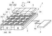
図1は、本実施の形態に係るX線検出器1を例示するための模式斜視図である。
なお、煩雑となるのを避けるために、図1においては、反射層6、防湿体7、充填部8、接合層9、壁体10などを省いて描いている。
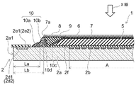
図2は、X線検出器1の模式断面図である。
なお、煩雑となるのを避けるために、図2においては、制御ライン(又はゲートライン)2c1、データライン(又はシグナルライン)2c2、信号処理部3、画像伝送部4などを省いて描いている。
放射線検出器であるX線検出器1は、放射線画像であるX線画像を検出するX線平面センサである。X線検出器1は、例えば、一般医療などに用いることができる。ただし、X線検出器1の用途は、一般医療に限定されるわけではない。
(X-ray detector)
First, the
FIG. 1 is a schematic perspective view for illustrating an
In order to avoid complication, in FIG. 1, the
FIG. 2 is a schematic cross-sectional view of the
In FIG. 2, the control line (or gate line) 2c1, the data line (or signal line) 2c2, the
The
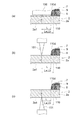
図1および図2に示すように、X線検出器1には、アレイ基板2、信号処理部3、画像伝送部4、シンチレータ5、反射層6、防湿体7、充填部8、接合層9、および壁体10が設けられている。
アレイ基板2は、基板2a、光電変換部2b、制御ライン2c1、データライン2c2、および保護層2fを有する。
As shown in FIGS. 1 and 2, the
The
基板2aは、板状を呈し、無アルカリガラスなどの透光性材料から形成されている。
光電変換部2bは、基板2aの一方の表面に複数設けられている。
光電変換部2bは、矩形状を呈し、制御ライン2c1とデータライン2c2とで画された領域に設けられている。複数の光電変換部2bは、マトリクス状に並べられている。
なお、1つの光電変換部2bは、1つの画素(pixel)に対応する。
The
A plurality of
The
One
複数の光電変換部2bのそれぞれには、光電変換素子2b1と、スイッチング素子である薄膜トランジスタ(TFT;Thin Film Transistor)2b2が設けられている。
また、信号電荷を蓄積する図示しない蓄積キャパシタを設けることができる。図示しない蓄積キャパシタは、例えば、矩形平板状を呈し、各薄膜トランジスタ2b2の下に設けることができる。ただし、光電変換素子2b1の容量によっては、光電変換素子2b1が図示しない蓄積キャパシタを兼ねることができる。
Each of the plurality of
Further, a storage capacitor (not shown) that stores signal charges can be provided. The storage capacitor (not shown) has, for example, a rectangular flat plate shape and can be provided under each thin film transistor 2b2. However, depending on the capacitance of the photoelectric conversion element 2b1, the photoelectric conversion element 2b1 can also serve as a storage capacitor (not shown).
光電変換素子2b1は、例えば、フォトダイオードなどとすることができる。
薄膜トランジスタ2b2は、図示しない蓄積キャパシタへの電荷の蓄積および放出のスイッチングを行う。薄膜トランジスタ2b2は、アモルファスシリコン(a−Si)やポリシリコン(P−Si)などの半導体材料を含むものとすることができる。薄膜トランジスタ2b2は、ゲート電極、ソース電極及びドレイン電極を有している。薄膜トランジスタ2b2のゲート電極は、対応する制御ライン2c1と電気的に接続される。薄膜トランジスタ2b2のソース電極は、対応するデータライン2c2と電気的に接続される。薄膜トランジスタ2b2のドレイン電極は、対応する光電変換素子2b1と図示しない蓄積キャパシタとに電気的に接続される。
The photoelectric conversion element 2b1 can be, for example, a photodiode.
The thin film transistor 2b2 performs switching of charge accumulation and emission to a storage capacitor (not shown). The thin film transistor 2b2 can include a semiconductor material such as amorphous silicon (a-Si) or polysilicon (P-Si). The thin film transistor 2b2 has a gate electrode, a source electrode, and a drain electrode. The gate electrode of the thin film transistor 2b2 is electrically connected to the corresponding control line 2c1. The source electrode of the thin film transistor 2b2 is electrically connected to the corresponding data line 2c2. The drain electrode of the thin film transistor 2b2 is electrically connected to the corresponding photoelectric conversion element 2b1 and a storage capacitor (not shown).
制御ライン2c1は、所定の間隔を開けて互いに平行に複数設けられている。制御ライン2c1は、例えば、行方向に延びている。
1つの制御ライン2c1は、基板2aの周縁近傍に設けられた複数の配線パッド2d1のうちの1つと電気的に接続されている。1つの配線パッド2d1には、フレキシブルプリント基板2e1に設けられた複数の配線のうちの1つが電気的に接続されている。フレキシブルプリント基板2e1に設けられた複数の配線の他端は、信号処理部3に設けられた図示しない制御回路とそれぞれ電気的に接続されている。
A plurality of control lines 2c1 are provided in parallel with each other at a predetermined interval. For example, the control line 2c1 extends in the row direction.
One control line 2c1 is electrically connected to one of a plurality of wiring pads 2d1 provided near the periphery of the
データライン2c2は、所定の間隔を開けて互いに平行に複数設けられている。データライン2c2は、例えば、行方向に直交する列方向に延びている。
1つのデータライン2c2は、基板2aの周縁近傍に設けられた複数の配線パッド2d2のうちの1つと電気的に接続されている。1つの配線パッド2d2には、フレキシブルプリント基板2e2に設けられた複数の配線のうちの1つが電気的に接続されている。フレキシブルプリント基板2e2に設けられた複数の配線の他端は、信号処理部3に設けられた図示しない増幅・変換回路とそれぞれ電気的に接続されている。
制御ライン2c1、およびデータライン2c2は、例えば、アルミニウムやクロムなどの低抵抗金属を用いて形成することができる。
A plurality of data lines 2c2 are provided in parallel with each other at a predetermined interval. The data line 2c2 extends, for example, in the column direction orthogonal to the row direction.
One data line 2c2 is electrically connected to one of a plurality of wiring pads 2d2 provided near the periphery of the
The control line 2c1 and the data line 2c2 can be formed using a low resistance metal such as aluminum or chromium, for example.
保護層2fは、光電変換部2b、制御ライン2c1、およびデータライン2c2を覆うように設けられている。
保護層2fは、例えば、酸化物絶縁材料、窒化物絶縁材料、酸窒化物絶縁材料、および樹脂材料の少なくとも1種を含む。
The
The
信号処理部3は、アレイ基板2の、シンチレータ5が設けられる側とは反対側に設けられている。
信号処理部3には、図示しない制御回路と、図示しない増幅・変換回路とが設けられている。
図示しない制御回路は、各薄膜トランジスタ2b2の動作、すなわちオン状態およびオフ状態を制御する。例えば、図示しない制御回路は、フレキシブルプリント基板2e1と配線パッド2d1と制御ライン2c1とを介して、制御信号S1を各制御ライン2c1毎に順次入力する。制御ライン2c1に入力された制御信号S1により薄膜トランジスタ2b2がオン状態となり、光電変換部2bからの信号電荷(画像データ信号S2)が受信できるようになる。
The
The
A control circuit (not shown) controls the operation of each thin film transistor 2b2, that is, the on state and the off state. For example, a control circuit (not shown) sequentially inputs the control signal S1 for each control line 2c1 via the flexible printed board 2e1, the wiring pad 2d1, and the control line 2c1. The thin film transistor 2b2 is turned on by the control signal S1 input to the control line 2c1, and the signal charge (image data signal S2) from the
図示しない増幅・変換回路は、例えば、複数の積分アンプ、複数の並列/直列変換器、および複数のアナログ−デジタル変換器を有している。
積分アンプは、データライン2c2と電気的に接続されている。
並列/直列変換器は、切り換えスイッチを介して積分アンプと電気的に接続されている。
アナログ−デジタル変換器は、並列/直列変換器と電気的に接続されている。
図示しない積分アンプは、データライン2c2と配線パッド2d2とフレキシブルプリント基板2e2とを介して、光電変換部2bからの画像データ信号S2を順次受信する。
An amplification / conversion circuit (not shown) includes, for example, a plurality of integration amplifiers, a plurality of parallel / serial converters, and a plurality of analog-digital converters.
The integrating amplifier is electrically connected to the data line 2c2.
The parallel / serial converter is electrically connected to the integrating amplifier via a changeover switch.
The analog-to-digital converter is electrically connected to the parallel / serial converter.
An integration amplifier (not shown) sequentially receives the image data signal S2 from the
そして、図示しない積分アンプは、一定時間内に流れる電流を積分し、その積分値に対応した電圧を並列/直列変換器へ出力する。この様にすれば、所定の時間内にデータライン2c2を流れる電流の値(電荷量)を電圧値に変換することが可能となる。
すなわち、積分アンプは、シンチレータ5において発生した蛍光の強弱分布に対応した画像データ情報を、電位情報へと変換する。
An integration amplifier (not shown) integrates the current flowing within a predetermined time, and outputs a voltage corresponding to the integration value to the parallel / serial converter. In this way, the value of the current (charge amount) flowing through the data line 2c2 within a predetermined time can be converted into a voltage value.
That is, the integrating amplifier converts image data information corresponding to the intensity distribution of fluorescence generated in the
図示しない並列/直列変換器は、電位情報へと変換された画像データ信号S2を順次直列信号に変換する。
図示しないアナログ−デジタル変換器は、直列信号に変換された画像データ信号S2をデジタル信号に順次変換する。
A parallel / serial converter (not shown) sequentially converts the image data signal S2 converted into potential information into a serial signal.
An analog-digital converter (not shown) sequentially converts the image data signal S2 converted into a serial signal into a digital signal.
画像伝送部4は、配線4aを介して、信号処理部3の図示しない増幅・変換回路と電気的に接続されている。なお、画像伝送部4は、信号処理部3と一体化されていてもよい。 画像伝送部4は、図示しないアナログ−デジタル変換器によりデジタル信号に変換された画像データ信号S2に基づいて、X線画像を構成する。構成されたX線画像のデータ(X線画像信号)は、画像伝送部4から外部の機器に向けて出力される。
The
シンチレータ5は、複数の光電変換素子2b1の上に設けられ、入射するX線を蛍光すなわち可視光に変換する。
シンチレータ5は、例えば、ヨウ化セシウム(CsI):タリウム(Tl)、あるいはヨウ化ナトリウム(NaI):タリウム(Tl)などを用いて形成することができる。この場合、真空蒸着法などを用いて、シンチレータ5を形成すれば、複数の柱状結晶の集合体からなるシンチレータ5が形成される。
なお、図2に例示をしたシンチレータ5は、真空蒸着法を用いて形成されたものである。
The
The
Note that the
また、シンチレータ5は、例えば、酸硫化ガドリニウム(Gd2O2S)などを用いて形成することもできる。この場合、複数の光電変換部2bごとに四角柱状のシンチレータ5が設けられるように、マトリクス状の溝部を形成することができる。
The
反射層6は、シンチレータ5の表面側(X線の入射面側)を覆うように設けられている。反射層6は、蛍光の利用効率を高めて感度特性を改善するために設けられる。反射層6は、例えば、酸化チタン(TiO2)などの光散乱性粒子を含む樹脂をシンチレータ5上に塗布することで形成することができる。
なお、反射層6は、必ずしも必要ではなく、必要に応じて設けるようにすればよい。
The
The
防湿体7は、空気中に含まれる水蒸気により、反射層6の特性やシンチレータ5の特性が劣化するのを抑制するために設けられている。
防湿体7は、反射層6(シンチレータ5)の上方を覆っている。この場合、防湿体7と反射層6の上面との間に隙間があってもよいし、防湿体7と反射層6の上面とが接触するようにしてもよい。
例えば、大気圧よりも減圧された環境において、防湿体7と、充填部8の上面とを接合すれば、大気圧により防湿体7と反射層6の上面が接触する。
The moisture-
The moisture-
For example, if the moisture-
防湿体7は、シンチレータ5の上方を覆い、周縁部近傍が充填部8の上面に接合されている。
X線の入射方向から見て、防湿体7の端面7aの位置は、有効画素エリアAよりは外側であって、壁体10の内面10cよりは内側となるようにすることができる。
この場合、X線の入射方向から見て、防湿体7の端面7aの位置が、壁体10の内面10cに近くなるようにすれば、充填部8の上面と防湿体7との封止性および信頼性を向上させることができる。
The moisture-
When viewed from the X-ray incident direction, the position of the
In this case, when the position of the
防湿体7は、透湿係数の小さい材料から形成することができる。
防湿体7は、例えば、アルミニウム、アルミニウム合金、あるいは、樹脂膜と無機材料(アルミニウムやアルミニウム合金などの金属、SiO2、SiON、Al2O3などのセラミック系材料)からなる膜とが積層された低透湿防湿膜(水蒸気バリアフィルム)などから形成することができる。
この場合、実効的な透湿係数がほとんどゼロであるアルミニウムやアルミニウム合金などを用いて防湿体7を形成すれば、防湿体7を透過する水蒸気をほぼ完全になくすことができる。
The moisture-
The moisture-
In this case, if the moisture-
また、防湿体7の厚み寸法は、X線の吸収や剛性などを考慮して決定することができる。この場合、防湿体7の厚み寸法を大きくしすぎるとX線の吸収が大きくなりすぎる。防湿体7の厚み寸法を小さくしすぎると剛性が低下して破損しやすくなる。
防湿体7は、例えば、厚み寸法が0.1mmのアルミニウム箔を用いて形成することができる。
Further, the thickness dimension of the moisture-
The moisture-
充填部8は、反射層6により覆われたシンチレータ5の側面と、壁体10の内面10cとの間に設けられている。
充填部8の上面の位置は、反射層6により覆われたシンチレータ5の上面の位置と同程度とすることができる。
この場合、充填部8の上面の位置は、反射層6により覆われたシンチレータ5の上面の位置と同じであってもよいし、反射層6により覆われたシンチレータ5の上面の位置より少し高くてもよいし、反射層6により覆われたシンチレータ5の上面の位置より少し低くてもよい。
なお、充填部8の上面の位置が、壁体10の頂部の位置より少し低くなるようにすれば、後述する充填を行う際に、充填部8を形成するための材料が壁体10の頂部を超えてあふれ出ないようにすることができる。
The filling
The position of the upper surface of the filling
In this case, the position of the upper surface of the filling
If the position of the upper surface of the filling
充填部8の材料は、透湿係数が小さいものとすることができる。
充填部8は、例えば、無機材料からなるフィラー材と、樹脂(例えば、エポキシ系樹脂など)を含む。
フィラー材は、例えば、タルク(滑石:Mg3Si4O10(OH)2)などから形成されたものとすることができる。
タルクは、低硬度の無機材質であり、滑り性が高い。そのため、タルクからなるフィラー材を高い濃度で含有させても、充填部8の形状変形が困難となることがない。
The material of the filling
The filling
The filler material can be made of, for example, talc (talc: Mg 3 Si 4 O 10 (OH) 2 ).
Talc is an inorganic material with low hardness and high slipperiness. Therefore, even if the filler material made of talc is contained at a high concentration, the shape deformation of the filling
タルクからなるフィラー材の粒径が、数μmから数十μm程度となるようにすれば、タルクからなるフィラー材の濃度(充填密度)を高めることができる。
タルクからなるフィラー材の濃度を高めれば、樹脂のみの場合と比較して透湿係数を1ケタ程度小さくすることができる。
例えば、タルクからなるフィラー材の濃度は、50重量%以上とすることができる。
If the particle size of the filler material made of talc is about several μm to several tens of μm, the concentration (filling density) of the filler material made of talc can be increased.
If the density | concentration of the filler material which consists of talc is raised, compared with the case where it is only resin, a moisture permeability coefficient can be made about 1 digit small.
For example, the density | concentration of the filler material which consists of talc can be 50 weight% or more.
充填部8の上面は、平坦であることが好ましい。
充填部8の上面が平坦であれば、充填部8の上面と防湿体7との封止性を確保し、且つ高い信頼性を得ることができる。
この場合、充填部8を形成するための材料の粘度を低めにすることで、充填部8の上面が平坦となるようにすることができる。
例えば、充填部8を形成するための材料の粘度が、室温で10Pa・sec程度となるようにすればよい。
The upper surface of the filling
If the upper surface of the filling
In this case, it is possible to make the upper surface of the filling
For example, the viscosity of the material for forming the filling
また、充填部8は、吸湿材と、樹脂(例えば、エポキシ系樹脂など)を含むものとすることもできる。
充填部8を形成するための材料は、例えば、吸湿材である塩化カルシウムと、バインダ樹脂(例えば、エポキシ系樹脂やシリコーン系樹脂など)と、溶媒を混合して作成したものとすることができる。
例えば、充填部8を形成するための材料の密度は2.1g/cc程度、当該材料の単位重量当たりの吸湿容量は27%程度、当該材料の粘度は室温で10Pa・sec程度とすることができる。
また、エポキシ化亜麻仁油などのエポキシ化植物油をさらに加えて、柔軟性を有する充填部8が形成されるようにすることができる。
柔軟性を有する充填部8とすれば、温度変化と部材間の熱膨張率差に起因する応力により剥がれが生じるのを抑制することができる。
Moreover, the filling
The material for forming the filling
For example, the density of the material for forming the filling
Further, an epoxidized vegetable oil such as epoxidized linseed oil can be further added to form a filling
If it is set as the filling
接合層9は、防湿体7と、充填部8の上面との間に設けられ、防湿体7の周縁近傍と充填部8とを接合している。
接合層9は、例えば、加熱や紫外線照射などを硬化の切っ掛けとする遅延硬化型接着剤、自然(常温)硬化型接着剤、および加熱硬化型接着剤のいずれかが硬化することで形成されたものとすることができる。
The
The
壁体10は、アレイ基板2の上に設けられ、シンチレータ5を囲んでいる。壁体10は、枠状を呈している。壁体10は、X線の入射方向から見て、シンチレータ5よりは外側であって、配線パッド2d1、2d2が設けられる領域よりは内側に設けられている。
この場合、壁体10が、配線パッド2d1、2d2が設けられる領域の近傍に設けられるようにすれば、充填部8の上面の面積を大きくすることができるので接合層9を大きくすることができる。そのため、充填部8の上面と接合層9との間の封止性および信頼性、および接合層9と防湿体7との間の封止性および信頼性を向上させることができる。
The
In this case, if the
壁体10の材料は、透湿係数が小さいものとすることが好ましい。
壁体10は、例えば、無機材料からなるフィラー材と、樹脂(例えば、エポキシ系樹脂など)を含むものとすることができる。
壁体10の材料は、例えば、充填部8の材料と同じとすることができる。
It is preferable that the material of the
The
The material of the
壁体10は、第1の部分10aと、第2の部分10bを有する。
第1の部分10aと基板2a(アレイ基板2)の周端面2a1との間の距離は、第2の部分10bと基板2aの周端面2a1との間の距離よりも短い。すなわち、第1の部分10aは、基板2aの周端面2a1の近傍に設けられている。
第1の部分10aの基板2aの表面からの高さは、第2の部分10bの基板2aの表面からの高さよりも低い。
壁体10は、積層構造を有する。
The
The distance between the
The height of the
The
また、壁体10の底面の中心と基板2aの周端面2a1との間の距離Laは、壁体10の頂部の中心と基板2aの周端面2a1との間の距離Lbよりも短い。すなわち、壁体10の底面の中心と壁体10の頂部の中心とを結ぶ線10dは、壁体10の頂部側に向かうに従いシンチレータ5に近づく方向に傾斜している。
また、壁体10の頂部側の断面積は、壁体10の底面側の断面積よりも小さくなっている。
The distance La between the center of the bottom surface of the
Further, the cross-sectional area on the top side of the
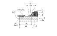
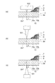
図3は、他の実施形態に係る壁体11を例示するための模式断面図である。
図3に示すように、壁体11も、第1の部分11aと、第2の部分11bを有する。
ただし、壁体11には、第2の部分11bの上に第3の部分11cがさらに設けられている。
FIG. 3 is a schematic cross-sectional view for illustrating a
As shown in FIG. 3, the
However, the
第1の部分11aと基板2a(アレイ基板2)の周端面2a1との間の距離は、第2の部分11bと基板2aの周端面2a1との間の距離よりも短い。第2の部分11bと基板2aの周端面2a1との間の距離は、第3の部分11cと基板2aの周端面2a1との間の距離よりも短い。
第1の部分11aの基板2aの表面からの高さは、第2の部分11bの基板2aの表面からの高さよりも低い。第2の部分11bの基板2aの表面からの高さは、第3の部分11cの基板2aの表面からの高さよりも低い。
すなわち、前述した壁体10は2層の積層構造を有していたが、壁体11は3層の積層構造を有している。なお、積層構造の層数は例示をしたものに限定されるわけではなく適宜変更することができる。
The distance between the
The height of the
That is, the
また、壁体11の底面の中心と基板2aの周端面2a1との間の距離Laは、壁体11の頂部の中心と基板2aの周端面2a1との間の距離Lbよりも短い。すなわち、壁体11の底面の中心と壁体11の頂部の中心とを結ぶ線11dは、壁体11の頂部側に向かうに従いシンチレータ5に近づく方向に傾斜している。
また、壁体11の頂部側の断面積は、壁体11の底面側の断面積よりも小さくなっている。
壁体11の材料は、例えば、壁体10の材料と同じとすることができる。
The distance La between the center of the bottom surface of the
The cross-sectional area on the top side of the
The material of the
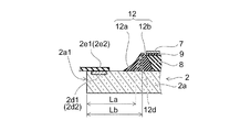
図4は、他の実施形態に係る壁体12を例示するための模式断面図である。
図4に示すように、壁体12も、第1の部分12aと、第2の部分12bを有する。
ただし、第1の部分12aの外側面と、第2の部分12bの外側面は、なだらかに繋がっている。
FIG. 4 is a schematic cross-sectional view for illustrating a
As shown in FIG. 4, the
However, the outer surface of the
第1の部分12aと基板2a(アレイ基板2)の周端面2a1との間の距離は、第2の部分12bと基板2aの周端面2a1との間の距離よりも短い。すなわち、第1の部分12aは、基板2aの周端面2a1の近傍に設けられている。
第1の部分12aの基板2aの表面からの高さは、第2の部分12bの基板2aの表面からの高さよりも低い。
The distance between the
The height of the
また、壁体12の底面の中心と基板2aの周端面2a1との間の距離Laは、壁体12の頂部の中心と基板2aの周端面2a1との間の距離Lbよりも短い。すなわち、壁体12の底面の中心と壁体12の頂部の中心とを結ぶ線12dは、壁体12の頂部側に向かうに従いシンチレータ5に近づく方向に傾斜している。
また、壁体12の頂部側の断面積は、壁体12の底面側の断面積よりも小さくなっている。
壁体12の材料は、例えば、壁体10の材料と同じとすることができる。
The distance La between the center of the bottom surface of the
The cross-sectional area on the top side of the
The material of the
次に、壁体10、11、12の効果について説明する。
前述した光電変換素子2b1や薄膜トランジスタ2b2は、一般的には静電気に対する耐性が低い。そのため、X線検出器1を製造する際には、製造工程中において発生した静電気を逃がす必要がある。例えば、全制御ライン2c1および全データライン2c2と電気的に接続され、複数の光電変換部2bが設けられた領域を囲む短絡用外周配線を設けるようにすれば、製造工程中において発生した静電気を短絡用外周配線を介して放電させることができる。
Next, effects of the
The photoelectric conversion element 2b1 and the thin film transistor 2b2 described above generally have low resistance to static electricity. Therefore, when manufacturing the
短絡用外周配線は、全制御ライン2c1および全データライン2c2と電気的に接続されているので、完成品には残しておくことができない。
そのため、枠状を呈する壁体10、11、12の外側において、基板2aを切断して短絡用外周配線を除去するようにしている。
基板2aの切断は、一般的にはスクライビング(割断加工)により行われる。スクライビングにおいては、基板2aの表面に浅い溝を形成し、基板2aに曲げ応力を加えた際に溝の角に応力集中を発生させるようにする。この様にすれば、基板2aの切断(割断)を容易に行うことができる。
溝の形成には、スクライビングホイール100やレーザ光101などが用いられる。
Since the short-circuiting outer peripheral wiring is electrically connected to all the control lines 2c1 and all the data lines 2c2, it cannot be left in the finished product.
Therefore, outside the
In general, the
For forming the groove, a
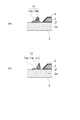
図5(a)〜(c)は、比較例に係る壁体110が設けられた基板2aの表面に溝を形成する様子を例示するための模式断面図である。
壁体110の底面の中心と基板2aの周端面2a1との間の距離Laは、壁体110の頂部の中心と基板2aの周端面2a1との間の距離Lbと同じである。すなわち、壁体110の底面の中心と壁体110の頂部の中心とを結ぶ線110dは、壁体110の底面に対して直角である。
FIGS. 5A to 5C are schematic cross-sectional views for illustrating a state in which grooves are formed on the surface of the
The distance La between the center of the bottom surface of the
図5(a)に示すように、スクライビングホイール100を用いて溝を形成する場合には、スクライビングホイール100と壁体110とが干渉しないようにする必要がある。そのため、壁体110と割断位置(基板2aの周端面2a1となる位置)との間の寸法Lが長くなるおそれがある。
As shown in FIG. 5A, when the grooves are formed using the
図5(b)、(c)に示すように、レーザ光101を用いて溝を形成する場合には、レーザ光の焦点距離が長いので、レーザ照射装置と壁体110との干渉は生じ難い。しかしながら、基板2aの照射位置における熱が壁体110に逃げることを考慮する必要がある。壁体110に逃げる熱が多くなると、照射位置における基板2aの温度が上がらず適切な溝が形成されなくなるおそれがある。この場合、レーザ光101の強度を上げると、溝の近傍にある配線パッド2d1、2d2などが損傷するおそれがある。そのため、レーザ光101を用いる場合にも壁体110と割断位置との間の寸法Lが長くなるおそれがある。
As shown in FIGS. 5B and 5C, when the groove is formed using the
寸法Lが長くなると、壁体110の外側に無駄なスペースが形成されるおそれがある。壁体110の外側に無駄なスペースが形成されると、X線検出器1の寸法の増加や重量の増加を招くおそれがある。
When the dimension L becomes long, a useless space may be formed outside the
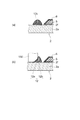
図6(a)〜(c)は、本実施の形態に係る壁体10が設けられた基板2aの表面に溝を形成する様子を例示するための模式断面図である。
スクライビングホイール100を用いて溝を形成する場合には、スクライビングホイール100と壁体10とが干渉しないようにする必要がある。しかしながら、図6(a)に示すように、スクライビングホイール100は、第1の部分10aの上方に入り込むことができる。そのため、壁体10と割断位置との間の寸法Lを短くすることができる。
6A to 6C are schematic cross-sectional views for illustrating a state in which grooves are formed on the surface of the
When the grooves are formed using the
また、レーザ光101を用いて溝を形成する場合には、基板2aの照射位置における熱が壁体110に逃げることを考慮する必要がある。しかしながら、図6(b)、(c)に示すように、第1の部分10aは体積が小さいので熱容量を小さくすることができる。そのため、基板2aの照射位置における熱が壁体110に逃げるのを抑制することができる。その結果、壁体10と割断位置との間の寸法Lを短くしても適切な溝を形成することが可能となる。
Moreover, when forming a groove | channel using the
寸法Lを短くすることができれば、壁体10の外側に無駄なスペースが形成されるのを抑制することができる。壁体10の外側に無駄なスペースが形成されるのを抑制することができれば、省スペース化を図ることができる。
なお、以上は壁体10の場合であるが、壁体11、12の場合も同様である。
If the dimension L can be shortened, it is possible to prevent a useless space from being formed outside the
Although the above is the case of the
また、平面形状が四角形の基板2aの一方の辺の近傍には配線パッド2d1(配線パッド2d2)が設けられ、対向する辺の近傍には配線パッド2d1(配線パッド2d2)が設けられない場合がある。すなわち、壁体と基板2aの周端面2a1との間には、配線パッド2d1、2d2が設けられる場合もあるが、配線パッド2d1、2d2が設けられない場合もある。そのため、方向によって、壁体と割断位置との間の寸法Lを変えることもできる。
例えば、寸法Lを短くすることができる領域には、壁体10、11、12を設け、寸法Lを短くすることができない領域には、例えば、壁体110を設けることができる。
すなわち、枠状の壁体の周方向における少なくとも一部の領域の、壁体の底面の中心と基板2aの周端面2a1との間の距離は、壁体の頂部の中心と基板2aの周端面2a1との間の距離よりも短くなるようにすることができる。
Further, there is a case where the wiring pad 2d1 (wiring pad 2d2) is provided in the vicinity of one side of the
For example, the
That is, the distance between the center of the bottom surface of the wall body and the peripheral end surface 2a1 of the
(X線検出器の製造方法)
次に、本実施の形態に係るX線検出器1の製造方法について例示をする。
まず、アレイ基板2を作成する。
アレイ基板2は、例えば、基板2aの上に光電変換部2b、制御ライン2c1、データライン2c2、配線パッド2d1、配線パッド2d2、および保護層2fなどを順次形成することで作成することができる。
アレイ基板2は、例えば、半導体製造プロセスを用いて作成することができる。
(Manufacturing method of X-ray detector)
Next, a method for manufacturing the
First, the
The
The
次に、複数の光電変換部2bを有するアレイ基板2の上に、シンチレータ5を形成する。
シンチレータ5は、複数の光電変換部2bが形成された領域を覆うように設ける。
シンチレータ5は、例えば、真空蒸着法などを用いて、ヨウ化セシウム:タリウムからなる膜をアレイ基板2の上に成膜することで形成することができる。この場合、シンチレータ5の厚み寸法は、600μm程度とすることができる。
Next, the
The
The
次に、シンチレータ5の表面側(X線の入射面側)の面を覆うように反射層6を形成する。
反射層6は、例えば、酸化チタンからなるサブミクロン粉体と、バインダ樹脂と、溶媒を混合して作成した材料をシンチレータ5上に塗布し、これを乾燥させることで形成することができる。
Next, the
The
次に、アレイ基板2の上に、シンチレータ5を囲む枠状の壁体10(壁体11、12)を形成する。
この場合、壁体10(壁体11、12)の底面の中心とアレイ基板2の周端面2aとの間の距離Laを、壁体10(壁体11、12)の頂部の中心とアレイ基板2の周端面2aとの間の距離Lbよりも短くする。
また、壁体10(壁体11、12)の高さが、反射層6により覆われたシンチレータ5の高さよりも少し高くなるようにすることができる。
壁体10(壁体11、12)は、例えば、壁体10(壁体11、12)の材料(例えば、タルクからなるフィラー材が添加されたエポキシ系樹脂など)を、反射層6により覆われたシンチレータ5の周囲に枠状に塗布し、これを硬化させることで形成することができる。
壁体10(壁体11、12)の材料の塗布は、例えば、ディスペンサー装置などを用いて行うことができる。
Next, a frame-like wall body 10 (
In this case, the distance La between the center of the bottom surface of the wall body 10 (
Further, the height of the wall body 10 (
The wall body 10 (
Application | coating of the material of the wall body 10 (
この場合、壁体10(壁体11)の材料の塗布と、硬化とを複数回繰り返すことで、積層構造を有する壁体10、11を形成することができる。
図7(a)は、壁体10の形成を例示するための模式断面図である。
図7(a)に示すように、まず、アレイ基板2の上に、第1の部分10aの材料を枠状に塗布し、これを硬化させて第1の部分10aを形成する。
この際、第1の部分10aの材料の粘度を低くすることで厚みが薄く断面積が大きい第1の部分10aを形成することができる。また、アレイ基板2とノズルの先端との間の距離を短くすることで、厚みが薄く断面積が大きい第1の部分10aを形成することもできる。
In this case, the
FIG. 7A is a schematic cross-sectional view for illustrating the formation of the
As shown in FIG. 7A, first, the material of the
At this time, the
続いて、第1の部分10aの上に、第2の部分10bの材料を枠状に塗布し、これを硬化させて第2の部分10bを形成する。
この際、第2の部分10bの材料の粘度を高くすることで厚みが厚く断面積が小さい第2の部分10bを形成することができる。また、アレイ基板2とノズルの先端との間の距離を長くすることで、厚みが厚く断面積が小さい第2の部分10bを形成することもできる。
Subsequently, the material of the
At this time, the
なお、第1の部分10aの材料と、第2の部分10bの材料は、同じであってもよいし、異なるものであってもよい。ただし、第1の部分10aと第2の部分10bの間に界面が形成されると、界面を介して水蒸気がシンチレータ5側に到達し易くなる。そのため、第1の部分10aの材料と、第2の部分10bの材料は、界面が形成され難いものとすることが好ましい。例えば、第1の部分10aの材料と、第2の部分10bの材料を同じにすれば、界面が形成され難くなる。
The material of the
図7(b)は、壁体11の形成を例示するための模式断面図である。
図7(b)に示すように、まず、アレイ基板2の上に、第1の部分11aの材料を枠状に塗布し、これを硬化させて第1の部分11aを形成する。
そして、図7(a)において例示をしたものと同様にして、第2の部分11b、第3の部分11cを順次形成する。
なお、第1の部分11aの材料と、第2の部分11bの材料と、第3の部分11cの材料は、同じであってもよいし、異なるものであってもよい。ただし、図7(a)において説明したように、界面が形成されないようにすることが好ましい。例えば、第1の部分11aの材料と、第2の部分11bの材料と、第3の部分11cの材料を同じにすれば、界面が形成され難くなる。
FIG. 7B is a schematic cross-sectional view for illustrating the formation of the
As shown in FIG. 7B, first, the material of the
Then, the
The material of the
また、アレイ基板2の上に壁体12の材料を塗布し、塗布された壁体12の材料を半硬化状態とし、半硬化状態とされた壁体12の材料を成形し、成形された壁体12の材料を硬化して壁体12を形成することもできる。
図8(a)、(b)は、壁体12の形成を例示するための模式工程断面図である。
まず、図8(a)に示すように、アレイ基板2の上に、例えば、フィラー材が添加された樹脂12cを枠状に塗布し、これを半硬化状態にする。樹脂12cの半硬化方法は、樹脂の種類により適宜選択することができる。例えば、樹脂12cが紫外線硬化型樹脂の場合には、紫外線の照射量や照射時間などにより樹脂12cを半硬化状態にする。樹脂12cが熱硬化型樹脂の場合には、加熱温度や加熱時間などにより樹脂12cを半硬化状態にする。樹脂12cが自然(常温)硬化型樹脂の場合には、硬化時間などにより樹脂12cを半硬化状態にする。
Further, the material of the
FIGS. 8A and 8B are schematic process cross-sectional views for illustrating the formation of the
First, as shown in FIG. 8A, for example, a
続いて、図8(b)に示すように、半硬化状態の樹脂12cに成形型102を押し当てて、樹脂12cを所望の形状に成形する。そして、成形された樹脂12cをさらに硬化させて壁体12を形成する。樹脂12cの硬化方法は、前述したものと同様に樹脂の種類により適宜選択することができる。
本実施の形態に係る壁体12の形成方法によれば、壁体12の内部に界面が形成されるのを抑制することができる。また形成工程の簡略化などを図ることができるので生産性を向上させることができる。
Subsequently, as shown in FIG. 8B, the molding die 102 is pressed against the
According to the method for forming the
なお、枠状の壁体を形成する工程において、枠状の壁体の周方向における少なくとも一部の領域の、壁体の底面の中心とアレイ基板2の周端面2aとの間の距離Laを、壁体の頂部の中心とアレイ基板2の周端面2aとの間の距離Lbよりも短くすることもできる。
In the step of forming the frame-shaped wall body, the distance La between the center of the bottom surface of the wall body and the
次に、反射層6により覆われたシンチレータ5の側面と、壁体10(壁体11、12)の内面との間に、フィラー材および吸湿材の少なくともいずれかと、樹脂とを含む材料を充填して充填部8を設ける。
充填部8は、例えば、フィラー材が添加された樹脂や吸湿材が添加された樹脂を、反射層6により覆われたシンチレータ5の側面と、壁体10(壁体11、12)の内面との間に充填し、これを硬化させることで形成することができる。
なお、充填は、例えば、ディスペンサー装置などを用いて行うことができる。
この場合、フィラー材が添加された樹脂や吸湿材が添加された樹脂の塗布と、硬化とを複数回繰り返すことで、充填部8を形成することができる。
なお、樹脂の塗布後に表面が平滑化するのを待って硬化を行う様にすることが好ましい。
Next, a material containing at least one of a filler material and a hygroscopic material and a resin is filled between the side surface of the
The filling
The filling can be performed using, for example, a dispenser device.
In this case, the filling
In addition, it is preferable to perform hardening after waiting for the surface to become smooth after application | coating of resin.
充填部8の上面の位置は、反射層6により覆われたシンチレータ5の上面の位置と同じであってもよいし、反射層6により覆われたシンチレータ5の上面の位置より少し高くてもよいし、反射層6により覆われたシンチレータ5の上面の位置より少し低くてもよい。
The position of the upper surface of the filling
充填部8を設けるようにすれば、充填部8の上面に防湿体7を接合することができるので、壁体10(壁体11、12)の外側に防湿体7を接合するためのスペースを設ける必要がなくなる。
そのため、X線検出器1の小型化や軽量化などを図ることができる。
また、充填部8を設けるようにすれば、防湿性能の向上、ひいては解像度特性の劣化の抑制を図ることもできる。
If the filling
Therefore, the
Further, if the filling
次に、防湿体7の周縁部近傍を、充填部8の上面に接合する。
例えば、充填部8の上面に紫外線硬化型接着剤を塗布し、紫外線硬化型接着剤の上に防湿体7を載せ、紫外線硬化型接着剤に紫外線を照射してこれを硬化させて接合層9を形成するとともに、防湿体7と、充填部8の上面とを接合する。
この場合、紫外線硬化型接着剤は、紫外線照射後に遅延して硬化が進行する遅延硬化型接着剤とすることが好ましい。
遅延硬化型接着剤を用いるようにすれば、紫外線照射後に、紫外線硬化型接着剤の上に防湿体7を載せればよいので、遮蔽物などがあって紫外線の照射が困難な場合にも接合を行うことができる。
なお、接着剤は、自然(常温)硬化型接着剤や加熱硬化型接着剤などであってもよい。 また、大気圧よりも減圧された環境(例えば、10KPa程度)において、防湿体7の周縁部近傍を充填部8の上面に接合することもできる。
Next, the vicinity of the periphery of the moisture-
For example, an ultraviolet curable adhesive is applied to the upper surface of the filling
In this case, the ultraviolet curable adhesive is preferably a delayed curable adhesive that cures with a delay after ultraviolet irradiation.
If a delayed-curing adhesive is used, the moisture-
The adhesive may be a natural (room temperature) curable adhesive or a heat curable adhesive. Further, the vicinity of the periphery of the moisture-
次に、フレキシブルプリント基板2e1、2e2を介して、アレイ基板2と信号処理部3を電気的に接続する。
また、配線4aを介して、信号処理部3と画像伝送部4を電気的に接続する。
その他、回路部品などを適宜実装する。
Next, the
Further, the
In addition, circuit components and the like are mounted as appropriate.
次に、図示しない筐体の内部にアレイ基板2、信号処理部3、画像伝送部4などを格納する。
そして、必要に応じて、光電変換素子2b1の異常や電気的な接続の異常の有無を確認する電気試験、X線画像試験などを行う。
以上のようにして、X線検出器1を製造することができる。
なお、製品の防湿信頼性や温度環境変化に対する信頼性を確認するために、高温高湿試験、冷熱サイクル試験などを実施することもできる。
Next, the
Then, as necessary, an electrical test, an X-ray image test, and the like for confirming whether there is an abnormality in the photoelectric conversion element 2b1 or an abnormality in electrical connection are performed.
The
In addition, in order to confirm the moisture-proof reliability of the product and the reliability against changes in the temperature environment, a high-temperature and high-humidity test, a cooling / heating cycle test, and the like can be performed.
以上、本発明のいくつかの実施形態を例示したが、これらの実施形態は、例として提示したものであり、発明の範囲を限定することは意図していない。これら新規な実施形態は、その他の様々な形態で実施されることが可能であり、発明の要旨を逸脱しない範囲で、種々の省略、置き換え、変更などを行うことができる。これら実施形態やその変形例は、発明の範囲や要旨に含まれるとともに、特許請求の範囲に記載された発明とその均等の範囲に含まれる。また、前述の各実施形態は、相互に組み合わせて実施することができる。 As mentioned above, although several embodiment of this invention was illustrated, these embodiment is shown as an example and is not intending limiting the range of invention. These novel embodiments can be implemented in various other forms, and various omissions, replacements, changes, and the like can be made without departing from the spirit of the invention. These embodiments and modifications thereof are included in the scope and gist of the invention, and are included in the invention described in the claims and equivalents thereof. Further, the above-described embodiments can be implemented in combination with each other.
1 X線検出器、2 アレイ基板、2a 基板、2b 光電変換部、3 信号処理部、4 画像伝送部、5 シンチレータ、6 反射層、7 防湿体、8 充填部、10 壁体、10a 第1の部分、10b 第2の部分、11 壁体、11a 第1の部分、11b 第2の部分、11c 第3の部分、12 壁体、12a 第1の部分、12b 第2の部分、La 距離、Lb 距離 1 X-ray detector, 2 array substrate, 2a substrate, 2b photoelectric conversion unit, 3 signal processing unit, 4 image transmission unit, 5 scintillator, 6 reflective layer, 7 moisture barrier, 8 filling unit, 10 wall body, 10a first Part, 10b second part, 11 wall body, 11a first part, 11b second part, 11c third part, 12 wall body, 12a first part, 12b second part, La distance, Lb distance
Claims (7)
前記複数の光電変換素子の上に設けられ、放射線を蛍光に変換するシンチレータと、
前記アレイ基板の上に設けられ、前記シンチレータを囲む枠状の壁体と、
を備え、
前記壁体の底面の中心と前記アレイ基板の周端面との間の距離は、前記壁体の頂部の中心と前記アレイ基板の周端面との間の距離よりも短い放射線検出器。 An array substrate having a plurality of photoelectric conversion elements;
A scintillator that is provided on the plurality of photoelectric conversion elements and converts radiation into fluorescence;
A frame-like wall provided on the array substrate and surrounding the scintillator;
With
The distance between the center of the bottom surface of the wall and the peripheral end surface of the array substrate is a radiation detector shorter than the distance between the center of the top of the wall and the peripheral end surface of the array substrate.
前記アレイ基板の上に、前記シンチレータを囲む枠状の壁体を形成する工程と、
を備え、
前記枠状の壁体を形成する工程において、前記壁体の底面の中心と前記アレイ基板の周端面との間の距離を、前記壁体の頂部の中心と前記アレイ基板の周端面との間の距離よりも短くする放射線検出器の製造方法。 Forming a scintillator on an array substrate having a plurality of photoelectric conversion elements;
Forming a frame-like wall body surrounding the scintillator on the array substrate;
With
In the step of forming the frame-shaped wall body, the distance between the center of the bottom surface of the wall body and the peripheral end surface of the array substrate is set between the center of the top of the wall body and the peripheral end surface of the array substrate. The manufacturing method of the radiation detector made shorter than the distance.
Priority Applications (1)
| Application Number | Priority Date | Filing Date | Title |
|---|---|---|---|
| JP2016137384A JP2018009826A (en) | 2016-07-12 | 2016-07-12 | Radiation detector and manufacturing method thereof |
Applications Claiming Priority (1)
| Application Number | Priority Date | Filing Date | Title |
|---|---|---|---|
| JP2016137384A JP2018009826A (en) | 2016-07-12 | 2016-07-12 | Radiation detector and manufacturing method thereof |
Publications (1)
| Publication Number | Publication Date |
|---|---|
| JP2018009826A true JP2018009826A (en) | 2018-01-18 |
Family
ID=60995306
Family Applications (1)
| Application Number | Title | Priority Date | Filing Date |
|---|---|---|---|
| JP2016137384A Pending JP2018009826A (en) | 2016-07-12 | 2016-07-12 | Radiation detector and manufacturing method thereof |
Country Status (1)
| Country | Link |
|---|---|
| JP (1) | JP2018009826A (en) |
-
2016
- 2016-07-12 JP JP2016137384A patent/JP2018009826A/en active Pending
Similar Documents
| Publication | Publication Date | Title |
|---|---|---|
| JP6523620B2 (en) | Radiation detector and method of manufacturing the same | |
| JP5905672B2 (en) | Radiation detector and manufacturing method thereof | |
| CN112912770B (en) | Radiation detection module, radiation detector, and method for manufacturing radiation module | |
| WO2016111093A1 (en) | Radiation detector and manufacturing method therefor | |
| JP2015021898A (en) | Radiation detector and manufacturing method thereof | |
| JP6729965B2 (en) | Radiation detector and manufacturing method thereof | |
| JP2017015428A (en) | Radiation detector and manufacturing method of same | |
| JP2017090090A (en) | Radiation detector and manufacturing method of the same | |
| JP6334149B2 (en) | Manufacturing method of radiation detector | |
| JP2017111082A (en) | Radiation detector and manufacturing method of the same | |
| JP6373624B2 (en) | Array substrate, radiation detector, and method of manufacturing radiation detector | |
| JP2020091236A (en) | Radiation detection module, radiation detector, and method for manufacturing radiation detection module | |
| JP6948815B2 (en) | Radiation detector | |
| JP2017044564A (en) | Radiation detector and manufacturing method thereof | |
| JP2018009826A (en) | Radiation detector and manufacturing method thereof | |
| JP2015232503A (en) | Radiation detector and manufacturing method of the same | |
| JP2018179510A (en) | Radiation detector, device for manufacturing radiation detector, and method for manufacturing radiation detector | |
| JP6818617B2 (en) | Radiation detectors, radiation detector manufacturing equipment, and radiation detector manufacturing methods | |
| JP6673600B2 (en) | Radiation detector and manufacturing method thereof | |
| JP6749038B2 (en) | Radiation detector and manufacturing method thereof | |
| JP2017078648A (en) | Radiation detector | |
| JP6356442B2 (en) | Radiation detector and manufacturing method thereof | |
| JP2017040622A (en) | Radiation detector and manufacturing method thereof | |
| JP6598518B2 (en) | Radiation detector | |
| JP2021105591A (en) | Radiation detection module, radiation detector and manufacturing method for radiation detection module |