JP2017524261A - LED carrier - Google Patents
LED carrier Download PDFInfo
- Publication number
- JP2017524261A JP2017524261A JP2017506875A JP2017506875A JP2017524261A JP 2017524261 A JP2017524261 A JP 2017524261A JP 2017506875 A JP2017506875 A JP 2017506875A JP 2017506875 A JP2017506875 A JP 2017506875A JP 2017524261 A JP2017524261 A JP 2017524261A
- Authority
- JP
- Japan
- Prior art keywords
- carrier
- led
- contact surface
- region
- substrate
- Prior art date
- Legal status (The legal status is an assumption and is not a legal conclusion. Google has not performed a legal analysis and makes no representation as to the accuracy of the status listed.)
- Pending
Links
Images


Classifications
-
- H—ELECTRICITY
- H01—ELECTRIC ELEMENTS
- H01L—SEMICONDUCTOR DEVICES NOT COVERED BY CLASS H10
- H01L33/00—Semiconductor devices with at least one potential-jump barrier or surface barrier specially adapted for light emission; Processes or apparatus specially adapted for the manufacture or treatment thereof or of parts thereof; Details thereof
- H01L33/48—Semiconductor devices with at least one potential-jump barrier or surface barrier specially adapted for light emission; Processes or apparatus specially adapted for the manufacture or treatment thereof or of parts thereof; Details thereof characterised by the semiconductor body packages
- H01L33/483—Containers
- H01L33/486—Containers adapted for surface mounting
-
- H—ELECTRICITY
- H01—ELECTRIC ELEMENTS
- H01C—RESISTORS
- H01C7/00—Non-adjustable resistors formed as one or more layers or coatings; Non-adjustable resistors made from powdered conducting material or powdered semi-conducting material with or without insulating material
- H01C7/10—Non-adjustable resistors formed as one or more layers or coatings; Non-adjustable resistors made from powdered conducting material or powdered semi-conducting material with or without insulating material voltage responsive, i.e. varistors
- H01C7/12—Overvoltage protection resistors
-
- H—ELECTRICITY
- H01—ELECTRIC ELEMENTS
- H01L—SEMICONDUCTOR DEVICES NOT COVERED BY CLASS H10
- H01L23/00—Details of semiconductor or other solid state devices
- H01L23/58—Structural electrical arrangements for semiconductor devices not otherwise provided for, e.g. in combination with batteries
- H01L23/60—Protection against electrostatic charges or discharges, e.g. Faraday shields
-
- H—ELECTRICITY
- H01—ELECTRIC ELEMENTS
- H01L—SEMICONDUCTOR DEVICES NOT COVERED BY CLASS H10
- H01L25/00—Assemblies consisting of a plurality of individual semiconductor or other solid state devices ; Multistep manufacturing processes thereof
- H01L25/16—Assemblies consisting of a plurality of individual semiconductor or other solid state devices ; Multistep manufacturing processes thereof the devices being of types provided for in two or more different main groups of groups H01L27/00 - H01L33/00, or in a single subclass of H10K, H10N, e.g. forming hybrid circuits
- H01L25/167—Assemblies consisting of a plurality of individual semiconductor or other solid state devices ; Multistep manufacturing processes thereof the devices being of types provided for in two or more different main groups of groups H01L27/00 - H01L33/00, or in a single subclass of H10K, H10N, e.g. forming hybrid circuits comprising optoelectronic devices, e.g. LED, photodiodes
-
- H—ELECTRICITY
- H01—ELECTRIC ELEMENTS
- H01L—SEMICONDUCTOR DEVICES NOT COVERED BY CLASS H10
- H01L33/00—Semiconductor devices with at least one potential-jump barrier or surface barrier specially adapted for light emission; Processes or apparatus specially adapted for the manufacture or treatment thereof or of parts thereof; Details thereof
- H01L33/48—Semiconductor devices with at least one potential-jump barrier or surface barrier specially adapted for light emission; Processes or apparatus specially adapted for the manufacture or treatment thereof or of parts thereof; Details thereof characterised by the semiconductor body packages
- H01L33/62—Arrangements for conducting electric current to or from the semiconductor body, e.g. lead-frames, wire-bonds or solder balls
-
- H—ELECTRICITY
- H01—ELECTRIC ELEMENTS
- H01L—SEMICONDUCTOR DEVICES NOT COVERED BY CLASS H10
- H01L33/00—Semiconductor devices with at least one potential-jump barrier or surface barrier specially adapted for light emission; Processes or apparatus specially adapted for the manufacture or treatment thereof or of parts thereof; Details thereof
- H01L33/48—Semiconductor devices with at least one potential-jump barrier or surface barrier specially adapted for light emission; Processes or apparatus specially adapted for the manufacture or treatment thereof or of parts thereof; Details thereof characterised by the semiconductor body packages
- H01L33/64—Heat extraction or cooling elements
- H01L33/644—Heat extraction or cooling elements in intimate contact or integrated with parts of the device other than the semiconductor body
-
- H—ELECTRICITY
- H01—ELECTRIC ELEMENTS
- H01L—SEMICONDUCTOR DEVICES NOT COVERED BY CLASS H10
- H01L25/00—Assemblies consisting of a plurality of individual semiconductor or other solid state devices ; Multistep manufacturing processes thereof
- H01L25/03—Assemblies consisting of a plurality of individual semiconductor or other solid state devices ; Multistep manufacturing processes thereof all the devices being of a type provided for in the same subgroup of groups H01L27/00 - H01L33/00, or in a single subclass of H10K, H10N, e.g. assemblies of rectifier diodes
- H01L25/04—Assemblies consisting of a plurality of individual semiconductor or other solid state devices ; Multistep manufacturing processes thereof all the devices being of a type provided for in the same subgroup of groups H01L27/00 - H01L33/00, or in a single subclass of H10K, H10N, e.g. assemblies of rectifier diodes the devices not having separate containers
- H01L25/075—Assemblies consisting of a plurality of individual semiconductor or other solid state devices ; Multistep manufacturing processes thereof all the devices being of a type provided for in the same subgroup of groups H01L27/00 - H01L33/00, or in a single subclass of H10K, H10N, e.g. assemblies of rectifier diodes the devices not having separate containers the devices being of a type provided for in group H01L33/00
- H01L25/0753—Assemblies consisting of a plurality of individual semiconductor or other solid state devices ; Multistep manufacturing processes thereof all the devices being of a type provided for in the same subgroup of groups H01L27/00 - H01L33/00, or in a single subclass of H10K, H10N, e.g. assemblies of rectifier diodes the devices not having separate containers the devices being of a type provided for in group H01L33/00 the devices being arranged next to each other
Abstract
本発明はLED(2)用の1つの担体(1)に関し、この担体は、1つの基体(5)を備え、ここでこの担体(1)上に搭載されたLED(2)を静電放電に対して保護するための1つの保護装置(6)がこの基体(5)内に一体化されている。【選択図】 図1The invention relates to a carrier (1) for an LED (2), which carrier comprises a substrate (5), in which the LED (2) mounted on the carrier (1) is electrostatically discharged. One protective device (6) for protecting against is integrated in the substrate (5). [Selection] Figure 1
Description
本発明はLED(発光ダイオード)用の担体に関する。 The present invention relates to a carrier for an LED (light emitting diode).
この担体は、この担体上に1つのLEDを、たとえばはんだ付けで固定するため、そしてこの担体がこのLEDの電気的接続部として用いられるために適している。LED担体システムの設計の際には、光の使用効率,寿命,および温度管理が常に重要な役割を果たしている。機能的課題の他に、解決すべき熱機械的並びに形状的問題もある。特にモバイル用途、たとえばスマートフォンまたはデジタルカメラにおけるLEDが組み込まれたカメラフラッシュでは、このLEDおよびこの担体は、出来る限り少ないスペースで、かつ出来る限り小さな部品高さが要求される。 The carrier is suitable for fixing one LED on the carrier, for example by soldering, and for the carrier being used as an electrical connection for the LED. When designing an LED carrier system, light usage efficiency, lifetime, and temperature management always play an important role. In addition to functional issues, there are also thermomechanical and geometric problems to be solved. Especially in mobile applications such as camera flashes incorporating LEDs in smartphones or digital cameras, the LEDs and the carrier are required to have as little space and as small a part height as possible.
LED用の担体に対するもう1つの要求条件は、このLEDから放出される光が遮られることを避けるために、上面に出来る限り他のデバイスが無いことである。 Another requirement for the carrier for the LED is that there are as few other devices as possible on the top surface to avoid blocking the light emitted from the LED.
上記の温度管理のために、上記のLEDと,上記の担体と,上記の担体表面との間で、出来る限り良好な熱的接触がなければならない。 For the above temperature control, there must be as good a thermal contact as possible between the LED, the carrier and the carrier surface.
さらに上記の担体は、静電放電(ESD=electrostatic discharge)に対する保護装置を備えなければならない。これはLEDがこのような静電放電に対して極めて敏感であるからである。公知のLED用担体では、このために適した保護デバイスがディスクリートな部品としてこの担体の上面上に設けられている。このディスクリートな部品は、とりわけ部品高さおよび必要スペースの観点から、またこの担体上に搭載されたLEDの放射特性の観点からも不利となり得る。 Furthermore, the carrier must be equipped with a protective device against electrostatic discharge (ESD). This is because LEDs are extremely sensitive to such electrostatic discharges. In known LED carriers, protective devices suitable for this are provided as discrete components on the upper surface of the carrier. This discrete component can be disadvantageous, especially from the standpoint of component height and required space, and from the standpoint of the emission characteristics of the LEDs mounted on this carrier.
さらにLED用担体は、この担体の回路基板へのはんだ付けの際に、このLEDとこの担体との間の結合部が融解せず、かつこのLEDの向きが変化されないように構成されていなければならない。 Further, the LED carrier must be configured so that the joint between the LED and the carrier does not melt and the orientation of the LED does not change when the carrier is soldered to the circuit board. Don't be.
本発明の課題は、改善された担体を提供することであり、この担体は、たとえば上述の観点の少なくとも1つに関して有利である。 The object of the present invention is to provide an improved carrier, which is advantageous, for example with respect to at least one of the above mentioned aspects.
これらの課題は請求項1に記載の担体によって解決される。
These problems are solved by the carrier according to
LED用の1つの担体が提示され、この担体は、1つの基体を備え、ここでこの担体上に固定されたLEDを静電放電に対して保護するための1つの保護装置がこの基体内に一体化されている。 A carrier for the LED is presented, the carrier comprising a substrate, in which a protective device for protecting the LED fixed on the carrier against electrostatic discharge is located in the substrate. It is integrated.
さらにこの担体は、1つの上面を備え、この上面には上記のLEDを固定するための少なくとも1つのコンタクト面領域が配設されている。このLEDは、好ましくははんだ付けによりこの少なくとも1つのコンタクト面領域上に固定される。 The carrier further comprises an upper surface on which at least one contact surface region for fixing the LED is arranged. The LED is fixed onto the at least one contact area, preferably by soldering.
従来の担体とは対照的に、上記の保護装置は上記のように、この担体の上面に配設されているのではなく、この基体内に一体化されている。以上により、この担体の部品高さおよび必要スペースは、上記の保護装置によって増大されない。本発明による担体は、こうしてより良好な小型化を可能とする。さらに、この担体の上面にはもはや上記の保護装置が無く、こうしてこの担体に搭載されたLEDの光放射特性は、この保護装置によって影響を受けない。 In contrast to conventional carriers, the protective device described above is not disposed on the top surface of the carrier as described above, but is integrated into the substrate. As described above, the component height and the necessary space of the carrier are not increased by the protection device. The carrier according to the invention thus makes it possible to achieve better miniaturization. Furthermore, the protective device is no longer on the upper surface of the carrier, and thus the light emission properties of the LED mounted on the carrier are not affected by the protective device.
保護装置とは、ここでは具体的には、静電放電の際に生じるような、高すぎる印加電圧による損傷からLEDを保護するために構成されている1つの装置を意味している。この保護装置は、このような電圧を除去して、このLEDに負荷を与えないようにするために構成されている。 By protective device is meant here in particular one device that is configured to protect the LED from damage due to an applied voltage that is too high, such as occurs during electrostatic discharge. The protection device is configured to remove such voltage and not load the LED.
上記の担体は、少なくとも1つのLEDを搭載するために適合していてよい。さらなる実施形態例においては、この担体は複数のLEDを固定するために適合していてよい。たとえばこの担体はコンタクト面領域(複数)を備えてよく、これらのコンタクト面領域に、複数の、たとえば3つのLEDがはんだ付けされてよい。この際これらの複数のLEDは、互いに異なる色を有してよい。 The carrier may be adapted for mounting at least one LED. In further example embodiments, the carrier may be adapted to secure a plurality of LEDs. For example, the carrier may comprise contact surface regions, to which a plurality of, for example, three LEDs may be soldered. In this case, the plurality of LEDs may have different colors.
上記の担体が複数のLEDを固定するために適合しているコンタクト面領域(複数)を備えると、これよりこの担体はさらに、この担体上に固定されたLED(複数)をこれらのコンタクト面領域を介して、そしてこの担体の基体上に取り付けられた金属面領域(複数)を介して互いに回路接続されるように構成することができる。これらの金属面領域は、これらのLEDの電気的接続部として用いることができる。たとえばこれらの金属面領域は、上記の担体の下面まで延在してよく、そして1つの配線基板との接続部として用いられてよい。 If the carrier comprises a contact surface area adapted for fixing a plurality of LEDs, the carrier further comprises a plurality of LEDs fixed on the carrier in the contact surface area. And can be configured to be connected to each other through the metal surface region (s) mounted on the substrate of the carrier. These metal surface regions can be used as electrical connections for these LEDs. For example, these metal surface regions may extend to the lower surface of the carrier and may be used as a connection with one wiring board.
上記の担体の上面には、2つのコンタクト面領域が配設されていてよく、ここでこれらのコンタクト面領域は、これらのコンタクト面領域の間のこの担体の上面上に、これらのコンタクト面領域の無い1つの中央領域が配置されるように、配設されており、ここで上記の基体において、少なくとも1つの熱的ビアが配設されており、この熱的ビアはこの担体の上面の中央領域をこの担体の下面と接続している。これらのコンタクト面領域上に1つのLEDが固定されると、これよりこの担体の上面の中央領域とこのLEDとの間に1つの間隙が形成され得る。この間隙にこのLEDから照射された熱が集中し得る。この担体の上面の中央領域とこの担体の下面とを接続している上記の熱的ビアは、ここでこの熱を効率よく逃がすことができる。 Two contact surface regions may be arranged on the upper surface of the carrier, wherein these contact surface regions are located on the upper surface of the carrier between these contact surface regions. Is arranged in such a way that there is one central region without air, where at least one thermal via is arranged in the above-mentioned substrate, the thermal via being in the middle of the upper surface of the carrier The region is connected to the underside of this carrier. When one LED is fixed on these contact surface regions, a gap can thereby be formed between the central region of the upper surface of the carrier and the LED. The heat irradiated from this LED can concentrate on this gap. The thermal vias connecting the central region of the upper surface of the carrier and the lower surface of the carrier can now efficiently dissipate this heat.
上記のコンタクト面領域(複数)が配設されている、上記の上面の領域には、ビア(複数)は無い。代替として、上記のコンタクト面領域(複数)上に固定される1つのLEDが上記のコンタクト面領域上に戴置され、この上面の領域のみにビアがなくともよい。これらのビアは、これらのコンタクト面領域の同一平面性および表面粗さに悪い影響を与え得る。これを避けるために、これらのビアは、これらのコンタクト面領域の領域には存在しないように配置されてよい。このようにして小さな同一平面性の許容差および小さな表面粗さを有するコンタクト面領域(複数)を達成することができる。 There is no via (s) in the upper surface region where the contact surface region (s) is disposed. Alternatively, one LED fixed on the contact surface region (s) may be placed on the contact surface region, and only the upper surface region need not have vias. These vias can adversely affect the coplanarity and surface roughness of these contact area regions. In order to avoid this, these vias may be arranged so as not to exist in the region of these contact surface regions. In this way, contact area (s) having a small coplanarity tolerance and a small surface roughness can be achieved.
具体的には、少なくとも1つのコンタクト面領域は、3μmより小さな同一平面性の許容差および/または1μmより小さな表面粗さを有する。これは上述のビアの配置の他に、上記の担体に一体化された内部電極および/または上記の担体に一体化されたヒートスプレッダの金属板がこの担体の上面に対して平行な方向に揃えられていることによっても達成されている。この場合、これらの内部電極および/または金属板はこの担体の表面と交差せず、そしてこれよりこの表面の平坦性の悪化をもたらさない。 Specifically, the at least one contact area has a coplanarity tolerance of less than 3 μm and / or a surface roughness of less than 1 μm. In addition to the arrangement of the vias described above, the internal electrode integrated with the carrier and / or the metal plate of the heat spreader integrated with the carrier are aligned in a direction parallel to the upper surface of the carrier. It is also achieved by. In this case, these internal electrodes and / or metal plates do not intersect the surface of the carrier and thus do not cause deterioration of the flatness of the surface.
上記基体は、1つのセラミック材料を含んでよい。具体的にはこの基体は、プラセオジム系酸化亜鉛(ZnO−Pr)またはビスマス系酸化亜鉛ン(ZnO−Bi)を含んでよい。これらの材料は、1つのバリスタとして上記の保護装置を構成することができる。これらの材料は、電圧依存の抵抗値を有する。一旦所定の閾値を越える1つの電圧が、上記の基体に一体化された内部電極(複数)に印加されると、このセラミック材料の抵抗値は一気に小さくなり、こうしてこれ以降電流がこの保護装置を通って流れることができ、そしてこれより上記のLEDを過度の電圧に対して保護することができる。 The substrate may comprise a single ceramic material. Specifically, the substrate may contain praseodymium-based zinc oxide (ZnO—Pr) or bismuth-based zinc oxide (ZnO—Bi). These materials can constitute the protective device as one varistor. These materials have voltage dependent resistance values. Once a voltage exceeding a predetermined threshold is applied to the internal electrode (s) integrated in the substrate, the resistance value of the ceramic material decreases at a stretch, so that the current is applied to the protective device thereafter. Can flow through and thus protect the LED against excessive voltages.
上記の保護装置は、上記の基体に一体化された内部電極(複数)を備えてよい。これらの内部電極は、Ag−Pdを含んでよい。代替として、他の材料、たとえば銀,パラジウム,または白金も可能である。 The protection device may include an internal electrode (s) integrated with the base body. These internal electrodes may contain Ag—Pd. Alternatively, other materials such as silver, palladium, or platinum are possible.
これらの内部電極は、上記の担体の上面に対して平行に揃えられていてよい。この平行に揃えられていることは、この上面が平坦に構成されることを可能とする。 These internal electrodes may be aligned parallel to the top surface of the carrier. This parallel alignment allows the top surface to be flat.
上記の保護装置は、上記の内部電極間に印加される電圧が1つの所定の値を越える場合に、電流がこの保護装置を通って流れることができるように構成されていてよい。 The protection device may be configured such that current can flow through the protection device when the voltage applied between the internal electrodes exceeds one predetermined value.
さらに上記の担体は、LEDの電気的接続のための金属面領域(複数)を備えてよく、これらの金属面領域は、この基体上に配設されており、そしてこのLEDのはんだ付け用に配設されているこの基体の上面から、この上面に対して反対側に配置されているこの基体の下面まで延在している。 Furthermore, the carrier may comprise metal surface areas for electrical connection of the LEDs, these metal surface areas being disposed on the substrate and for soldering the LEDs. It extends from the upper surface of the substrate disposed to the lower surface of the substrate disposed on the opposite side of the upper surface.
ここでこれらの金属面領域は、具体的にはこの基体の上面上で、直接このLEDのはんだ付けのためのコンタクト面領域と電気的に接続されていてよい。さらにこの基体は、1つのSMD(SMD=Surface Mounted Device)部品であってよく、このSMD部品は1つの配線基板上でのはんだ付けに適している。この際、この基体の下面まで達しているこれらの金属面領域を介して、この配線基板との1つの電気的接続部を生成することができる。こうしてこれらの金属面領域は、1つの配線基板との、この担体上に搭載されたLEDの電気的接続部を生成することができる。 Here, these metal surface regions may be electrically connected to the contact surface region for soldering the LED directly, specifically on the upper surface of the substrate. Further, the substrate may be one SMD (SMD = Surface Mounted Device) component, and this SMD component is suitable for soldering on one wiring board. At this time, one electrical connection with the wiring board can be generated through these metal surface regions reaching the lower surface of the substrate. These metal surface areas can thus create an electrical connection of the LED mounted on this carrier with one wiring board.
さらにこれらの金属面領域は、温度管理に有利である。動作中は上記の担体上に配設されたLEDは、熱を放射する。この際このLEDの下面からの熱もこの担体の上面へ照射される。この担体の上面上に配設されているコンタクト面領域(複数)は、金属から生成することができ、良好な熱伝導性を有することができる。これらのコンタクト面領域は、特にこの担体に照射された熱の大部分を直接上記の金属面領域(複数)へ伝達することができる。これらの金属面領域はこの基体の外面(複数)上に配設されているので、これらの金属面領域はこの熱を良好にこの担体の外部環境に放射することができる。以上によりこれらの金属面領域は、この熱を速やかに逃がし、そして基板およびLEDの過熱をこうして防止することを可能とする。 Furthermore, these metal surface regions are advantageous for temperature management. During operation, the LEDs disposed on the carrier emit heat. At this time, heat from the lower surface of the LED is also applied to the upper surface of the carrier. The contact surface region (s) disposed on the top surface of the carrier can be generated from metal and have good thermal conductivity. These contact surface regions can transfer most of the heat irradiated to the carrier directly to the metal surface region (s). Since these metal surface areas are arranged on the outer surface (s) of the substrate, these metal surface areas can radiate this heat well to the outside environment of the carrier. Thus, these metal surface regions allow this heat to escape quickly and thus prevent overheating of the substrate and the LED.
さらに加えて、この担体は上記の基体の外面(複数)上にさらなる金属面領域を備えてよい。これらのさらなる金属面領域は、上記のLEDの電気的接続のために用いられてよい。しかしながらこれらのさらなる金属面領域は、熱的な課題を満足するだけでなく、熱の放散にも寄与する。 In addition, the carrier may comprise additional metal surface areas on the outer surface (s) of the substrate. These additional metal surface areas may be used for electrical connection of the LEDs described above. However, these additional metal surface areas not only satisfy thermal challenges but also contribute to heat dissipation.
上記の金属面領域および/または上記のコンタクト面領域は、銀,ニッケル,および金、または銀,ニッケル,および錫を含む1つの層構造を備えてよい。 The metal surface region and / or the contact surface region may comprise a single layer structure comprising silver, nickel, and gold, or silver, nickel, and tin.
さらに1つのヒートスプレッダ(Heat Spreader)が上記の担体に一体化されていてよい。このヒートスプレッダは、この担体上に搭載されたLEDから放射される熱を速やかに消散するために用いることができる。このようにしてこのヒートスプレッダは、この担体の温度管理を大幅に単純化することができる。 Furthermore, one heat spreader (Heat Spreader) may be integrated into the carrier. This heat spreader can be used to quickly dissipate the heat emitted from the LEDs mounted on this carrier. In this way, the heat spreader can greatly simplify the temperature management of the carrier.
このヒートスプレッダは、上記の基体に一体化された金属板(複数)を備えてよく、これらの金属板は、上記の金属面(複数)とこの担体の基体上で熱的に接続されていてよい。上記のLEDからこの担体へ照射された熱は、このようにして容易に消散することができ、ここでこの熱はこれらの金属板を介して上記の金属面領域に与えられ、そしてそこから外部環境に放射される。このヒートスプレッダのこれらの金属板は、Ag−Pdを含んでよい。 The heat spreader may comprise a plurality of metal plates integrated with the substrate, and the metal plates may be thermally connected to the metal surface (s) and the substrate of the carrier. . The heat emitted from the LED to the carrier can be easily dissipated in this way, where the heat is applied to the metal surface area via these metal plates and from there externally Radiated to the environment. These metal plates of the heat spreader may contain Ag-Pd.
このヒートスプレッダのこれらの金属板は、上記の担体の上面に対して平行に揃えられていてよい。 These metal plates of the heat spreader may be aligned parallel to the top surface of the carrier.
このヒートスプレッダは、上記の一体化された内部電極よりもこの担体の上面の近くに配設されていてよい。このヒートスプレッダが出来る限り上記のLEDの近くに配設されていることが、このヒートスプレッダの機能のために、このLEDから放射される熱を良好に捕集することができるようにするために決定的に重要である。 The heat spreader may be disposed closer to the top surface of the carrier than the integrated internal electrode. The heat spreader is arranged as close as possible to the LED as described above, so that the heat radiated from the LED can be well collected for the function of the heat spreader. Is important to.
上記の基体の上面上には、LEDをはんだ付けするためのコンタクト面領域(複数)が設けられていてよい。これらのコンタクト面領域上には、1つのLEDが、たとえば共晶はんだによって、または金−金接合によってはんだ付けされてよい。 On the upper surface of the substrate, a contact surface region (plurality) for soldering the LED may be provided. On these contact area, one LED may be soldered, for example by eutectic solder or by a gold-gold joint.
上記の担体は、1つのSMD部品であってよく、この部品は、1つの配線基板上でのはんだ付けに適している。 The carrier may be a single SMD component, which is suitable for soldering on a single wiring board.
上記の担体は、複数のLEDの固定用のコンタクト面領域(複数)を備えてよい。ここでこの担体はさらに、コンタクト面領域(複数)の1つの適合した構成によって、複数のLEDが互いに回路接続されるように、構成されていてよい。ここで代替として、この担体は、これらのLEDの各々がそれぞれ対応して構成された外部電極を介して接続されるように構成されていてよい。 The carrier may include a plurality of contact surface regions for fixing a plurality of LEDs. Here, the carrier may further be configured such that a plurality of LEDs are connected to one another by one adapted configuration of the contact surface region (s). Alternatively, the carrier may be configured such that each of these LEDs is connected via a correspondingly configured external electrode.
上記のLEDの固定用のコンタクト面領域は、1つの積層構造を備えてよく、この積層構造は、少なくとも1つの金層および少なくとも1つの錫層を備え、ここでこの少なくとも1つの金層および少なくとも1つの錫層の厚さは、この積層構造における金と錫との比が75:25〜85:15となるように、好ましくは80:20となるように選択されている。この構成は、融点の低下、たとえば300〜320℃への低下を可能とする。 The fixing contact surface area of the LED may comprise one laminated structure, which comprises at least one gold layer and at least one tin layer, wherein the at least one gold layer and at least The thickness of one tin layer is selected such that the gold to tin ratio in this laminated structure is 75:25 to 85:15, preferably 80:20. This configuration makes it possible to lower the melting point, for example, to 300 to 320 ° C.
以下に本発明の有利な態様(複数)を説明する。これらの態様の間の参照関係を簡単にするために、これらの態様には連番が付されている。これらの態様の特徴は、これらのそれぞれの態様に対して関連し得るだけでなく、他の態様の特徴とも協働することが可能である。 The advantageous embodiment (s) of the invention are described below. In order to simplify the reference relationship between these aspects, these aspects are numbered sequentially. The features of these aspects may not only be relevant to each of these aspects, but can also work with features of other aspects.
(第1の態様)
LED用の担体であって、1つの基体を備え、この担体上に搭載されたLEDを、静電放電に対して保護するために、1つの保護装置が当該基体内に一体化されていることを特徴とする担体。
(First aspect)
A carrier for an LED, which is provided with a single substrate, and in order to protect the LED mounted on the carrier against electrostatic discharge, a single protective device is integrated in the substrate. A carrier characterized by.
(第2の態様)
上記の第1の態様による担体であって、上記基体は、1つのセラミック材料を含むことを特徴とする担体。
(Second aspect)
A carrier according to the first aspect, wherein the substrate comprises a ceramic material.
(第3の態様)
上記の第1または第2の態様による担体であって、上記基体は、プラセオジム系酸化亜鉛またはビスマス系酸化亜鉛含むことを特徴とする担体。
(Third aspect)
The carrier according to the first or second aspect, wherein the substrate contains praseodymium-based zinc oxide or bismuth-based zinc oxide.
(第4の態様)
上記の第1または第2の態様による担体であって、上記保護装置は、上記基体内に一体化された内部電極(複数)を備えることを特徴とする担体。
(Fourth aspect)
The carrier according to the first or second aspect, wherein the protection device includes an internal electrode (s) integrated in the base.
(第5の態様)
上記の第4の態様による担体であって、上記内部電極(複数)はAg−Pdを含むことを特徴とする担体。
(5th aspect)
The carrier according to the fourth aspect, wherein the internal electrode (s) contain Ag-Pd.
(第6の態様)
上記の第4または第5の態様による担体であって、上記保護装置は、上記内部電極(複数)に印加される電圧が1つの所定の値を越える場合に、電流が上記保護装置を通って流れることができるように構成されていることを特徴とする担体。
(Sixth aspect)
The carrier according to the fourth or fifth aspect, wherein the protection device has a current passing through the protection device when a voltage applied to the internal electrode (s) exceeds one predetermined value. A carrier characterized by being configured to flow.
(第7の態様)
上記の第1乃至第6の態様による担体であって、上記担体は、LEDの電気的接続のための金属面領域(複数)を備え、当該金属面領域は、上記基体上に配設されており、そして当該LEDのはんだ付け用に配設されている上記基体の上面から、当該上面に対して反対側に配設されている上記基体の下面まで延在していることを特徴とする担体。
(Seventh aspect)
The carrier according to any one of the first to sixth aspects, wherein the carrier includes a metal surface region (multiple) for electrical connection of the LED, and the metal surface region is disposed on the substrate. And a carrier extending from the upper surface of the substrate disposed for soldering the LED to the lower surface of the substrate disposed on the opposite side of the upper surface. .
(第8の態様)
上記の第7の態様による担体であって、上記の金属面領域および/または上記のコンタクト面領域は、銀,ニッケル,および金、または銀,ニッケル,および錫を含む1つの層構造を備えていることを特徴とする担体。
(Eighth aspect)
The carrier according to the seventh aspect, wherein the metal surface region and / or the contact surface region comprises a single layer structure comprising silver, nickel, and gold, or silver, nickel, and tin. A carrier characterized in that
(第9の態様)
上記の第1乃至第8の態様による担体であって、1つのヒートスプレッダが上記の担体に一体化されており、このヒートスプレッダは、上記の基体に一体化された金属板(複数)を備えていることを特徴とする担体。
(Ninth aspect)
A carrier according to the first to eighth aspects, wherein one heat spreader is integrated with the carrier, and the heat spreader includes a metal plate (plural) integrated with the base. A carrier characterized by the above.
(第10の態様)
上記の第9の態様による担体であって、上記ヒートスプレッダの上記金属板は、上記金属面領域と接続されていることを特徴とする担体。
(Tenth aspect)
The carrier according to the ninth aspect, wherein the metal plate of the heat spreader is connected to the metal surface region.
(第11の態様)
上記の第9または第10の態様による担体であって、上記ヒートスプレッダは、上記の一体化された内部電極よりも上記の担体の上面の近くに配設されていることを特徴とする担体。
(Eleventh aspect)
The carrier according to the ninth or tenth aspect, wherein the heat spreader is disposed closer to the upper surface of the carrier than the integrated internal electrode.
(第12の態様)
上記の第1乃至第11の態様による担体であって、上記の担体は、1つのSMD部品であり、当該部品は、1つの配線基板上でのはんだ付けに適していることを特徴とする担体。
(Twelfth aspect)
The carrier according to any of the first to eleventh aspects, wherein the carrier is one SMD component, and the component is suitable for soldering on one wiring board. .
(第13の態様)
上記の第1乃至第12の態様による担体であって、上記の担体は、複数のLEDの固定用のコンタクト面領域(複数)を備えることを特徴とする担体。
(13th aspect)
The carrier according to any one of the first to twelfth aspects, wherein the carrier includes contact surface regions (plurality) for fixing a plurality of LEDs.
以下では、図を参照して、本発明を詳細に説明する。
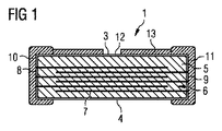
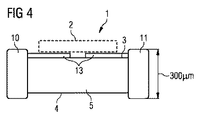
図1〜4は、1つのLED2用の1つの担体1の1つの第1の実施形態例を示す。図1は、この担体1の1つの断面を示す。図2は、この担体1の上面3上の平面図を示す。図3は、この担体1の下面4上の平面図を示す。図4は、この担体1の側面図を示す。さらに図4には、この担体1上に搭載された1つのLED2が、点線で示されている。
1-4 show a first exemplary embodiment of one
担体1は1つのSMD部品(SMD=Surface-mounted device)である。これよりこの担体1は、1つの配線基板(不図示)上にはんだを用いて固定するのに適している。
The
さらにこの担体1は、その上に1つのLED2が搭載されるように構成されている。具体的には、この担体1は、その上にはんだを用いて1つのLED2が固定されるように構成されている。
Further, the
この担体1は、1つの基体5を備える。この基体5は、ほぼ直方体である。この基体5は、1つのセラミック材料を含む。具体的には、この基体5はこのセラミック材料から成っている。このセラミック材料は、プラセオジム系酸化亜鉛またはビスマス系酸化亜鉛であってよい。
The
基体5内には、担体1上に搭載されている1つのLED2を、静電放電(ESD=electrostatic discharge)に対して保護するための1つの保護装置6が一体化されている。この保護装置6は、この基体5内に一体化された内部電極(複数)7を備える。
In the
これらの電極7の各々は、担体1の上面3に対して平行な1つのレベル面において延在しており、ここでこの担体1の上面3は、LED2を固定することができる面である。内部電極(複数)7もこの担体1の上面3に対して平行に揃えられている。この平行に揃えられていることが、垂直方向に並んだ内部電極7として示されている。
Each of these electrodes 7 extends in one level plane parallel to the
担体1の上面3から、この上面3の反対側にあるこの担体1の下面4への方向において、これらの内部電極7は交互に、この担体1の1つの第1の端面8まで、あるいはこの担体1の第2の端面9まで延在している。この担体1の第1の端面8上には、1つの第1の金属面領域10が取り付けられている。この第1の金属面領域10は、この第1の端面8の全長に渡って延在しており、そしてこの基体5の上面3へも、また下面4へも突出している。この担体1の第2の端面9上には、1つの第2の金属面領域11が取り付けられている。この第2の金属面領域11は、この第2の端面9の全長に渡って延在しており、そしてこの基体5の上面3へも、また下面4へも突出している。内部電極(複数)7は、上面3から下面4への方向において交互に、この第1の金属面領域10およびこの第2の金属面領域11と接続されている。
In the direction from the
この第1および第2の金属面領域10,11は、Ag,Ni,および/またはAuを含む。具体的には、これらの金属面領域10,11は、Ag,Ni,Auから成る積層構造を備え、ここでAgは最下層を形成している。Auの代わりにSnが用いられてもよい。
The first and second
この第1および第2の金属面領域10,11は、担体1上に搭載されているLED2の電気的接続に用いられる。以上より上記の保護装置は、これら2つの金属面領域10,11からこのLED2に印加される電圧が、上記の内部電極(複数)7間にも印加されるように構成されている。
The first and second
上記の保護装置は1つのバリスタを形成する。通常の電圧では、内部電極(複数)7間には、基体5のセラミック材料を通って全く電流が流れることができない。これはこのセラミック材料が非常に大きな抵抗を有するからである。この抵抗はしかしながら電圧依存である。2つの隣り合った内部電極間に印加されている電圧が1つの所定の閾値を越えると、このセラミック材料の抵抗は一気に低下する。ここでこれらの隣り合った内部電極7間に電流が流れることができ、そして印加されている電圧は低下され得る。このようにして、静電放電によって発生するような高電圧が発生した際に、この電圧がLED2に損傷をもたらすことが防止される。この保護装置6は、この電圧がこの保護装置6によって低下され、LED2に負荷されないようにするために用いられる。
The protective device forms one varistor. Under normal voltage, no current can flow between the internal electrodes 7 through the ceramic material of the
内部電極(複数)7は、銀−パラジウム(Ag−Pd)を含むかまたは銀−パラジウム(Ag−Pd)から成っている。 The internal electrode (s) 7 contains silver-palladium (Ag—Pd) or consists of silver-palladium (Ag—Pd).
更に基体5は、ガラスパッシベーション12によって被覆されている。第1および第2の金属面領域10,11は、このガラスパッシベーション上に外側に配設されている。内部電極(複数)7は、このガラスパッシベーションを貫通して突出しており、こうして第1および第2の金属面領域10,11と電気的に接続されている。
Furthermore, the
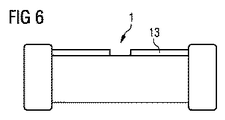
担体1の上面3上には、2つのコンタクト面領域13が配設されている。これらのコンタクト面領域13は、Ag,Niおよび/またはAuを含む。具体的には、これらのコンタクト面領域13は、Ag,Ni,およびAuから成る1つの積層構造を備え、ここでAgは最下層を形成している。Auの代わりにSnが用いられてもよい。担体1のこれらのコンタクト面領域13上には、図4に示すように、1つのLED2を固定することができる。これらのコンタクト面領域13は、このLED2が1つの共晶はんだ処理において、このコンタクト面領域13にはんだ付けされることができるように構成されている。ここでこのはんだ処理は、たとえば銀−鉛共晶はんだ処理であってよい。代替としてまたは補完的に、これらのコンタクト面領域13は、上記のLED2を金−金接合(Gold-Gold Interconnect;GGI)の接着処理でこれらのコンタクト面領域13上に固定することができるように構成されている。共晶はんだ処理は、はんだの融点を低下することを可能とする。
Two
担体1は、さらなるLED(複数)2を搭載するためのさらなる他のコンタクト面領域13を備えてよい。
The
この第1および第2の金属面領域10,11は、コンタクト面領域13より大きな厚さを有してよい。
The first and second
代替としてコンタクト面領域13は、1つの積層構造を備えてよく、この積層構造は少なくとも、1つの金を含む層および1つの錫を含む層を備える。好ましくは、この積層構造の少なくとも1つの層は金から成っており、そして少なくとも1つの層は錫から成っている。
Alternatively, the
この積層構造は、たとえば上記の上面3上に直接配設された1つのチタン下地層を備えてよい。 このチタン下地層の上に、1つのニッケル層が配設されていてよい。このニッケル層の上に、1つの第1の金層,1つの第1の錫層,1つの第2の金層,および1つの第2の錫層がこの順で配設されていてよい。このチタン下地層は、スパッタリングを用いて生成することができ、そしてたとえば0.1μmの厚さを有してよい。この積層構造のこれらのさらなる層は、電気めっきで生成されてよい。上記のニッケル層は、2μmの厚さを有してよい。上記の金層は、0.8μmの厚さを有してよい。上記の錫層は、0.2μmの厚さを有してよい。
This stacked structure may include, for example, one titanium underlayer directly disposed on the
これらの金層および錫層の厚さは、上記のコンタクト面領域13の積層構造において、金と錫との比が75:25〜85:15となるように、好ましくは80:20となるように互いに調整されていてよい。この比は、このコンタクト面領域の融解温度の低下をもたらす。このようにして300℃〜320℃の融解温度を達成することができる。このようにして共晶はんだ付けを可能とすることができる。
The thickness of the gold layer and the tin layer is preferably 80:20 so that the ratio of gold and tin is 75:25 to 85:15 in the laminated structure of the
上記の下地層のスパッタリング、およびこれに続いてこの下地層の上にこのコンタクト面領域13のさらなる層を電気めっきで生成することによって、コンタクト面領域13が完成され、このコンタクト面領域はとりわけ小さな同一平面性の許容差およびとりわけ小さな表面粗さを有する。たとえばこのコンタクト面領域13は、3μmより小さな同一平面性の許容差を有する。さらにこのコンタクト面領域13は、1μmより小さな表面粗さを有する。
The
担体1は、100μm〜500μmの厚さを有し、好ましくは150μm〜350μmの厚さを有する。ここでこの厚さは、担体1の上面3から下面4までの距離を与える。さらにこの担体1は、200μm〜2000μmの幅を有し、好ましくは350μm〜1600μmの幅を有する。さらにこの担体1は、100μm〜1500μmの長さを有し、好ましくは150μm〜1000μmの長さを有する。ここでこの幅は、端面8,9の面法線の方向におけるこの担体1の大きさを与える。この長さは、端面8,9に沿った、上面3と下面4とを結ぶ線の方向に対して垂直な方向におけるこの担体1の大きさを与える。
The
さらにこの担体1は、その下面4上に、少なくとも1つの熱的コンタクト面領域(不図示)を備えてよい。これらの熱的コンタクト面領域は、この担体1が搭載されている1つの配線基板との、この担体1の熱的接続を改善することができる。これらの熱的コンタクト面領域は、Ag,Niおよび/またはAuを含んでよい。具体的には、これらの熱的コンタクト面領域は、Ag,Ni,およびAuから成る1つの積層構造を備え、ここでAgは基体5上に直に配設されていてよい。Auの代わりにSnが用いられてもよい。
Furthermore, the
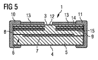
図5は、担体1の1つの第2の実施形態例を示す。第2の実施形態例による担体1は、さらに1つのヒートスプレッダ14(Heat Spreader)を備え、このヒートスプレッダは、担体1の基体5内に一体化されている。このヒートスプレッダ14は、金属板(複数)15を備える。このヒートスプレッダ14のこれらの金属板15は、2つのグループに分割されている。第1のグループの金属板15は、第1の端面8上の第1の金属面領域10と接続されている。第2のグループの金属板15は、第2の端面9上の第2の金属面領域11と接続されている。
FIG. 5 shows one second embodiment of the
動作中には、担体1上に搭載されたLED2は、多量の熱を放射し得る。この際この熱は担体1へも放射される。ヒートスプレッダ14の金属板(複数)15は、発生する熱を速やかに放散するために用いられる。この際これらの金属板は、金属面領域10,11を介した熱放散を助け、そしてこれによりさらに良好な熱の放散に用いられる。
During operation, the
このようにして担体1上に搭載されたLED2ならびにこの担体1の基体5の過熱を防止することができる。この熱は、金属板(複数)15からそれぞれの金属面領域10,11へ放散され、ここからこの熱はより容易に放射することができる。このヒートスプレッダ14の金属板15は、銀−パラジウムを含み、あるいは銀−パラジウムから成っている。
In this way, overheating of the
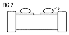
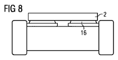
図6,7,および8は、どのようにしてLED2が担体1に搭載されるかを示す。まず図6には、LED2の無い担体1が示されている。図7は第1の搭載ステップの後の担体1を示し、ここでははんだ16がこの担体1のコンタクト面領域13上に取り付けられている。図8は、LED2がこの担体1上に固定された後の、担体1を示す。LED2は、コンタクト面領域(複数)13上に戴置され、ここではんだ16は担体1のLED2との機械的結合に用いられる。そしてこのはんだ16は硬化する。
6, 7 and 8 show how the
図9は、担体1の1つの第3の実施形態例を示す。図9には、この担体1の上面3上の平面図が示されている。上面3上には、全部で4つのコンタクト面領域13が配設されている。これらのコンタクト面領域13の各々は、それぞれ1つの金属面領域10,11,19を介して電気的に接続されている。この担体は、このために、第1および第2の金属面領域10,11の他に、さらなる金属面領域(複数)19を備える。ここでこれらの金属面領域10,11,19の各々は、担体1の上面3から、端面8,9の1つまたは外側面17,18の1つを介して、この担体1の下面4まで延在している。これらの外側面17,18は、それぞれ上面3と下面4とを結合しており、端面8,9に対して垂直になっている。図9に示す担体1は、2つのLEDの固定用に構成されている。
FIG. 9 shows one third embodiment of the
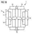
図10は、担体1の1つの第4の実施形態例を示す。図10にも、この担体1の上面3上の平面図が示されている。上面3上には、全部で8つのコンタクト面領域13が配設されており、こうしてこの担体は4つのLEDの実装用に適合している。これらのコンタクト面領域13の各々は、それぞれ1つの金属面領域10,11,19を介して電気的に接続されている。ここでこれらの金属面領域10,11,19の各々は、担体1の上面3から、端面8,9の1つまたは上記の外側面の1つを介して、この担体1の下面4まで延在している。
FIG. 10 shows one fourth embodiment of the
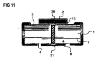
図11および図12は、担体1の1つの第5の実施形態例の担体を示す。ここで図11は1つの断面を示し、図12は1つの平面図を示す。
11 and 12 show a carrier of one fifth embodiment of the
担体1の上面3上には、2つのコンタクト面領域13が配設されており、これらのコンタクト面領域上には1つのLEDをはんだ付けすることができる。これらのコンタクト面領域の間には、上面3の中央領域20が存在している。LED2がこれらのコンタクト面領域13に固定されていると、これによりこの中央領域において、LED2と担体1との間に1つの間隙が形成される。
Two
この担体は、さらに少なくとも1つの熱的ビア21を備え、この熱的ビアは、この上面3の中央領域をこの担体の下面3と結合している。ここではこの担体1は、3つの熱的ビアを備える。これらの熱的ビアは、LED2から上記の間隙に放射された熱を、下面へ逃がすことを可能とする。こうしてこれらの熱的ビアは、この構造を熱的に改善することを可能とする。
The carrier further comprises at least one thermal via 21, which couples the central region of the
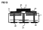
図13および14は、担体の1つの第6の実施形態例を示す。 Figures 13 and 14 show one sixth embodiment of the carrier.
この担体は、金属面領域10,11を全く備えていない。その代りこの担体はさらなるビア(複数)22を備え、これらのビアはコンタクト面領域13の接続のため、および基体内に一体化されている内部電極の接続のために用いられる。これらのさらなるビア22は、LED2が直に戴置されていない領域におけるコンタクト面領域13に接している。これによりこれらのビアは、LED2が戴置されている領域におけるコンタクト面領域13の同一平面性および表面粗さに悪影響を与えない。
This carrier does not have any
これらのコンタクト面領域13は、金対錫の比が80:20を有する上述の積層構造を備える。
These
1 : 担体
2 : LED
3 : 上面
4 : 下面
5 : 基体
6 : 保護装置
7 : 内部電極
8 : 第1の端面
9 : 第2の端面
10 : 第1の金属面領域
11 : 第2の金属面領域
12 : ガラスパッシベーション
13 : コンタクト面領域
14 : ヒートスプレッダ
15 : 金属板
16 : はんだ
17 : 外側面
18 : 外側面
19 : さらなる金属面領域
20 : 中央領域
21 : 熱的ビア
22 : さらなるビア
1: Carrier 2: LED
3: Upper surface 4: Lower surface 5: Base body 6: Protection device 7: Internal electrode 8: First end surface 9: Second end surface 10: First metal surface region 11: Second metal surface region 12: Glass passivation 13 : Contact surface region 14: Heat spreader 15: Metal plate 16: Solder 17: Outer side surface 18: Outer side surface 19: Additional metal surface region 20: Central region 21: Thermal via 22: Further via
Claims (16)
1つの基体(5)を備え、
前記担体は1つの上面(3)を備え、当該上面上に1つのLED(2)を固定するための少なくとも1つの第1のコンタクト面領域(13)を備え、
前記担体(1)上に固定されたLED(2)を、静電放電に対して保護するために、1つの保護装置(6)が前記基体(5)内に一体化されている、
ことを特徴とする担体。 A carrier (1) for one LED (2),
Comprising one substrate (5),
The carrier comprises one upper surface (3), on which at least one first contact surface region (13) for fixing one LED (2),
In order to protect the LED (2) fixed on the carrier (1) against electrostatic discharge, one protective device (6) is integrated in the substrate (5),
A carrier characterized by the above.
前記担体(1)の前記上面(3)上には、1つの第2のコンタクト面領域(13)が配設されており、前記担体(1)の上面(3)上に、前記第1のコンタクト面領域と前記第2のコンタクト面領域との間で、前記第1および前記第2のコンタクト面領域の無い、1つの中央領域(20)が配設されるように、前記第1および前記第2のコンタクト面領域が配設されており、
前記基体(5)には、少なくとも1つの熱的ビア(21)が配設されており、当該熱的ビアは、前記担体の(1)の上面(3)の前記中央領域(20)を前記担体(1)の下面(4)と結合している、
ことを特徴とする担体。 The carrier according to claim 1,
One second contact surface region (13) is disposed on the upper surface (3) of the carrier (1), and the first surface is formed on the upper surface (3) of the carrier (1). Between the contact surface region and the second contact surface region, the first and the first and the second contact surface regions are disposed so that one central region (20) without the first and second contact surface regions is disposed. A second contact surface region is disposed;
The substrate (5) is provided with at least one thermal via (21), the thermal via extending the central region (20) of the upper surface (3) of the carrier (1) into the central region (20). Connected to the lower surface (4) of the carrier (1),
A carrier characterized by the above.
前記保護装置(6)は、前記基体(5)内に一体化された複数の内部電極(7)を備え、
前記複数の内部電極(7)は、前記担体(1)の前記上面(3)に対して平行に揃えられている、
ことを特徴とする担体。 The carrier according to any one of claims 1 to 5,
The protection device (6) includes a plurality of internal electrodes (7) integrated in the base (5),
The plurality of internal electrodes (7) are aligned parallel to the upper surface (3) of the carrier (1).
A carrier characterized by the above.
前記担体(1)は、前記LED(2)の電気的接続のための複数の金属面領域(10,11)を備え、当該金属面領域は、前記基体(5)上に配設されており、そして当該基体(5)の上面(3)から、当該上面(3)に対して反対側に配置されている当該基体(5)の下面(4)まで延在しており、
前記ヒートスプレッダの前記金属板(15)は、前記金属面領域(10,11)と接続されている、
ことを特徴とする担体。 The carrier according to claim 10 or 11,
The carrier (1) includes a plurality of metal surface regions (10, 11) for electrical connection of the LED (2), and the metal surface regions are disposed on the base (5). And extending from the upper surface (3) of the substrate (5) to the lower surface (4) of the substrate (5) disposed on the opposite side of the upper surface (3),
The metal plate (15) of the heat spreader is connected to the metal surface region (10, 11),
A carrier characterized by the above.
前記保護装置(6)は、前記基体(5)内に一体化された複数の内部電極(7)を備え、
前記ヒートスプレッダ(14)は、前記一体化された内部電極(7)よりも前記担体(1)の上面(3)の近くに配設されている、
ことを特徴とする担体。 The carrier according to any one of claims 10 to 12,
The protection device (6) includes a plurality of internal electrodes (7) integrated in the base (5),
The heat spreader (14) is disposed closer to the upper surface (3) of the carrier (1) than the integrated internal electrode (7).
A carrier characterized by the above.
Applications Claiming Priority (5)
| Application Number | Priority Date | Filing Date | Title |
|---|---|---|---|
| DE102014111363.2 | 2014-08-08 | ||
| DE102014111363 | 2014-08-08 | ||
| DE102014115375.8 | 2014-10-22 | ||
| DE102014115375.8A DE102014115375A1 (en) | 2014-08-08 | 2014-10-22 | Carrier for an LED |
| PCT/EP2015/068280 WO2016020537A1 (en) | 2014-08-08 | 2015-08-07 | Carrier for an led |
Related Child Applications (1)
| Application Number | Title | Priority Date | Filing Date |
|---|---|---|---|
| JP2019003096A Division JP2019083328A (en) | 2014-08-08 | 2019-01-11 | LED carrier |
Publications (1)
| Publication Number | Publication Date |
|---|---|
| JP2017524261A true JP2017524261A (en) | 2017-08-24 |
Family
ID=55134667
Family Applications (2)
| Application Number | Title | Priority Date | Filing Date |
|---|---|---|---|
| JP2017506875A Pending JP2017524261A (en) | 2014-08-08 | 2015-08-07 | LED carrier |
| JP2019003096A Pending JP2019083328A (en) | 2014-08-08 | 2019-01-11 | LED carrier |
Family Applications After (1)
| Application Number | Title | Priority Date | Filing Date |
|---|---|---|---|
| JP2019003096A Pending JP2019083328A (en) | 2014-08-08 | 2019-01-11 | LED carrier |
Country Status (6)
| Country | Link |
|---|---|
| US (1) | US9978912B2 (en) |
| EP (1) | EP3178117B1 (en) |
| JP (2) | JP2017524261A (en) |
| CN (1) | CN106575692B (en) |
| DE (2) | DE102014115375A1 (en) |
| WO (1) | WO2016020537A1 (en) |
Families Citing this family (3)
| Publication number | Priority date | Publication date | Assignee | Title |
|---|---|---|---|---|
| DE102016122014A1 (en) * | 2016-11-16 | 2018-05-17 | Epcos Ag | Power module with reduced susceptibility to defects and use thereof |
| DE102017118490A1 (en) * | 2017-08-14 | 2019-02-14 | Tdk Electronics Ag | LED module |
| DE102017126268A1 (en) | 2017-11-09 | 2019-05-09 | Osram Opto Semiconductors Gmbh | A support, substrate and support assembly and method of making a support |
Citations (8)
| Publication number | Priority date | Publication date | Assignee | Title |
|---|---|---|---|---|
| JP2005150386A (en) * | 2003-11-14 | 2005-06-09 | Stanley Electric Co Ltd | Semiconductor device and its manufacturing method |
| JP2006295079A (en) * | 2005-04-14 | 2006-10-26 | Tdk Corp | Light emitting device |
| JP2008109079A (en) * | 2006-09-26 | 2008-05-08 | Kyocera Corp | Wiring board for surface mounting type light-emitting element, and light-emitting device |
| JP2008270325A (en) * | 2007-04-17 | 2008-11-06 | Matsushita Electric Ind Co Ltd | Electrostatic discharge protective component and light-emitting diode module using the same |
| JP2011523778A (en) * | 2008-05-21 | 2011-08-18 | エプコス アクチエンゲゼルシャフト | Electrical component assembly |
| JP2011187855A (en) * | 2010-03-11 | 2011-09-22 | Panasonic Corp | Method of manufacturing multilayer ceramic substrate |
| JP2012074501A (en) * | 2010-09-28 | 2012-04-12 | Stanley Electric Co Ltd | Optical semiconductor element, light-emitting diode, and method of manufacturing them |
| JP2014116411A (en) * | 2012-12-07 | 2014-06-26 | Kyocera Corp | Substrate for mounting light emitting element and light emitting device |
Family Cites Families (11)
| Publication number | Priority date | Publication date | Assignee | Title |
|---|---|---|---|---|
| JP3475910B2 (en) | 2000-05-24 | 2003-12-10 | 株式会社村田製作所 | Electronic component, method of manufacturing electronic component, and circuit board |
| US7279724B2 (en) * | 2004-02-25 | 2007-10-09 | Philips Lumileds Lighting Company, Llc | Ceramic substrate for a light emitting diode where the substrate incorporates ESD protection |
| WO2006106901A1 (en) * | 2005-04-01 | 2006-10-12 | Matsushita Electric Industrial Co., Ltd. | Led component and method for manufacturing same |
| JP4915058B2 (en) * | 2005-06-06 | 2012-04-11 | パナソニック株式会社 | LED component and manufacturing method thereof |
| US7505239B2 (en) | 2005-04-14 | 2009-03-17 | Tdk Corporation | Light emitting device |
| WO2007058438A1 (en) * | 2005-11-18 | 2007-05-24 | Amosense Co., Ltd. | Electronic parts packages |
| US20090020876A1 (en) * | 2007-07-20 | 2009-01-22 | Hertel Thomas A | High temperature packaging for semiconductor devices |
| US8536584B2 (en) * | 2007-11-14 | 2013-09-17 | Cree, Inc. | High voltage wire bond free LEDS |
| DE102008024480A1 (en) * | 2008-05-21 | 2009-12-03 | Epcos Ag | Electrical component arrangement |
| EP2418700B1 (en) * | 2010-08-09 | 2017-11-01 | LG Innotek Co., Ltd. | Light emitting device |
| DE102012104494A1 (en) * | 2012-05-24 | 2013-11-28 | Epcos Ag | light emitting diode device |
-
2014
- 2014-10-22 DE DE102014115375.8A patent/DE102014115375A1/en not_active Withdrawn
-
2015
- 2015-08-07 JP JP2017506875A patent/JP2017524261A/en active Pending
- 2015-08-07 WO PCT/EP2015/068280 patent/WO2016020537A1/en active Application Filing
- 2015-08-07 US US15/501,162 patent/US9978912B2/en active Active
- 2015-08-07 CN CN201580042669.XA patent/CN106575692B/en active Active
- 2015-08-07 DE DE202015009825.8U patent/DE202015009825U1/en active Active
- 2015-08-07 EP EP15750372.3A patent/EP3178117B1/en active Active
-
2019
- 2019-01-11 JP JP2019003096A patent/JP2019083328A/en active Pending
Patent Citations (8)
| Publication number | Priority date | Publication date | Assignee | Title |
|---|---|---|---|---|
| JP2005150386A (en) * | 2003-11-14 | 2005-06-09 | Stanley Electric Co Ltd | Semiconductor device and its manufacturing method |
| JP2006295079A (en) * | 2005-04-14 | 2006-10-26 | Tdk Corp | Light emitting device |
| JP2008109079A (en) * | 2006-09-26 | 2008-05-08 | Kyocera Corp | Wiring board for surface mounting type light-emitting element, and light-emitting device |
| JP2008270325A (en) * | 2007-04-17 | 2008-11-06 | Matsushita Electric Ind Co Ltd | Electrostatic discharge protective component and light-emitting diode module using the same |
| JP2011523778A (en) * | 2008-05-21 | 2011-08-18 | エプコス アクチエンゲゼルシャフト | Electrical component assembly |
| JP2011187855A (en) * | 2010-03-11 | 2011-09-22 | Panasonic Corp | Method of manufacturing multilayer ceramic substrate |
| JP2012074501A (en) * | 2010-09-28 | 2012-04-12 | Stanley Electric Co Ltd | Optical semiconductor element, light-emitting diode, and method of manufacturing them |
| JP2014116411A (en) * | 2012-12-07 | 2014-06-26 | Kyocera Corp | Substrate for mounting light emitting element and light emitting device |
Also Published As
| Publication number | Publication date |
|---|---|
| EP3178117A1 (en) | 2017-06-14 |
| CN106575692B (en) | 2019-07-05 |
| WO2016020537A1 (en) | 2016-02-11 |
| DE202015009825U1 (en) | 2020-07-22 |
| US20170229617A1 (en) | 2017-08-10 |
| CN106575692A (en) | 2017-04-19 |
| US9978912B2 (en) | 2018-05-22 |
| EP3178117B1 (en) | 2020-07-15 |
| DE102014115375A1 (en) | 2016-02-11 |
| JP2019083328A (en) | 2019-05-30 |
Similar Documents
| Publication | Publication Date | Title |
|---|---|---|
| JP6262725B2 (en) | Light emitting diode device | |
| JP5698424B2 (en) | Light-emitting diode substrate incorporating ESD protection in the substrate | |
| TWI512915B (en) | Electronic element assembly structure | |
| JP6195319B2 (en) | Light emitting diode device | |
| JP6874022B2 (en) | Multi LED system, carrier and LED system | |
| KR102350223B1 (en) | Carrier for semiconductor devices with passive cooling function | |
| JP5548194B2 (en) | Electrical component assembly comprising a varistor and a semiconductor component | |
| JP6117809B2 (en) | ESD protection device and device comprising ESD protection device and LED | |
| JP2011523778A (en) | Electrical component assembly | |
| JP2019083328A (en) | LED carrier | |
| EP3669396B1 (en) | Led module | |
| JP2017527998A (en) | Light emitting diode device | |
| JP2008270327A (en) | Electrostatic discharge protecting component and light-emitting diode module using the same | |
| JP2008270325A (en) | Electrostatic discharge protective component and light-emitting diode module using the same | |
| US10818641B2 (en) | Multi-LED system | |
| KR100674857B1 (en) | Led pkg and its method having improved esd capability | |
| JP2008227137A (en) | Electrostatic countermeasure component and light-emitting diode module using the same | |
| JP2014216480A (en) | Wiring board and electronic equipment | |
| US20160013166A1 (en) | Light emitting module | |
| JP2008270326A (en) | Electrostatic discharge protecting component and light-emitting diode module using the same | |
| JP2008227138A (en) | Electrostatic countermeasure component and light-emitting diode group employing the same | |
| JP2013058617A (en) | Mounting substrate and light emitting device | |
| JP2014086631A (en) | Package for light-emitting element and light-emitting device |
Legal Events
| Date | Code | Title | Description |
|---|---|---|---|
| A621 | Written request for application examination |
Free format text: JAPANESE INTERMEDIATE CODE: A621 Effective date: 20170403 |
|
| A977 | Report on retrieval |
Free format text: JAPANESE INTERMEDIATE CODE: A971007 Effective date: 20180124 |
|
| A131 | Notification of reasons for refusal |
Free format text: JAPANESE INTERMEDIATE CODE: A131 Effective date: 20180214 |
|
| A601 | Written request for extension of time |
Free format text: JAPANESE INTERMEDIATE CODE: A601 Effective date: 20180509 |
|
| A521 | Request for written amendment filed |
Free format text: JAPANESE INTERMEDIATE CODE: A523 Effective date: 20180712 |
|
| A02 | Decision of refusal |
Free format text: JAPANESE INTERMEDIATE CODE: A02 Effective date: 20180912 |
|
| A521 | Request for written amendment filed |
Free format text: JAPANESE INTERMEDIATE CODE: A523 Effective date: 20190111 |
|
| A521 | Request for written amendment filed |
Free format text: JAPANESE INTERMEDIATE CODE: A821 Effective date: 20190111 |
|
| A911 | Transfer to examiner for re-examination before appeal (zenchi) |
Free format text: JAPANESE INTERMEDIATE CODE: A911 Effective date: 20190204 |
|
| A912 | Re-examination (zenchi) completed and case transferred to appeal board |
Free format text: JAPANESE INTERMEDIATE CODE: A912 Effective date: 20190412 |