JP2016218385A - 光走査装置及び画像形成装置 - Google Patents
光走査装置及び画像形成装置 Download PDFInfo
- Publication number
- JP2016218385A JP2016218385A JP2015106223A JP2015106223A JP2016218385A JP 2016218385 A JP2016218385 A JP 2016218385A JP 2015106223 A JP2015106223 A JP 2015106223A JP 2015106223 A JP2015106223 A JP 2015106223A JP 2016218385 A JP2016218385 A JP 2016218385A
- Authority
- JP
- Japan
- Prior art keywords
- imaging lens
- optical scanning
- scanning device
- image forming
- temperature sensor
- Prior art date
- Legal status (The legal status is an assumption and is not a legal conclusion. Google has not performed a legal analysis and makes no representation as to the accuracy of the status listed.)
- Granted
Links
- 230000003287 optical effect Effects 0.000 title claims abstract description 36
- 239000000853 adhesive Substances 0.000 claims abstract description 32
- 230000001070 adhesive effect Effects 0.000 claims abstract description 31
- 238000003384 imaging method Methods 0.000 claims description 54
- 230000002093 peripheral effect Effects 0.000 claims description 2
- 238000000034 method Methods 0.000 description 11
- 239000011347 resin Substances 0.000 description 4
- 229920005989 resin Polymers 0.000 description 4
- 230000007547 defect Effects 0.000 description 2
- 238000005452 bending Methods 0.000 description 1
- 238000004140 cleaning Methods 0.000 description 1
- 230000007423 decrease Effects 0.000 description 1
- 238000010586 diagram Methods 0.000 description 1
- 230000001678 irradiating effect Effects 0.000 description 1
- 229920001187 thermosetting polymer Polymers 0.000 description 1
Images


Classifications
-
- G—PHYSICS
- G03—PHOTOGRAPHY; CINEMATOGRAPHY; ANALOGOUS TECHNIQUES USING WAVES OTHER THAN OPTICAL WAVES; ELECTROGRAPHY; HOLOGRAPHY
- G03G—ELECTROGRAPHY; ELECTROPHOTOGRAPHY; MAGNETOGRAPHY
- G03G15/00—Apparatus for electrographic processes using a charge pattern
- G03G15/04—Apparatus for electrographic processes using a charge pattern for exposing, i.e. imagewise exposure by optically projecting the original image on a photoconductive recording material
- G03G15/043—Apparatus for electrographic processes using a charge pattern for exposing, i.e. imagewise exposure by optically projecting the original image on a photoconductive recording material with means for controlling illumination or exposure
- G03G15/0435—Apparatus for electrographic processes using a charge pattern for exposing, i.e. imagewise exposure by optically projecting the original image on a photoconductive recording material with means for controlling illumination or exposure by introducing an optical element in the optical path, e.g. a filter
-
- G—PHYSICS
- G03—PHOTOGRAPHY; CINEMATOGRAPHY; ANALOGOUS TECHNIQUES USING WAVES OTHER THAN OPTICAL WAVES; ELECTROGRAPHY; HOLOGRAPHY
- G03G—ELECTROGRAPHY; ELECTROPHOTOGRAPHY; MAGNETOGRAPHY
- G03G21/00—Arrangements not provided for by groups G03G13/00 - G03G19/00, e.g. cleaning, elimination of residual charge
- G03G21/20—Humidity or temperature control also ozone evacuation; Internal apparatus environment control
Abstract
Description
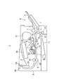
図1は、本実施形態における画像形成装置としてのレーザープリンタ1の概略構成を示す断面図である。
上記実施形態では、光走査装置30をレーザープリンタに搭載した例について説明したが、これに限ったものではなく、例えば光走査装置30をプロジェクター等に搭載するようにしてもよい。
30 光走査装置
33 光源
34 ポリゴンミラー(偏向部)
40 接着剤
101 温度センサー
101a センサー本体
101b 配線
312 突出座部
312a 凹部
312b 配線溝
Claims (3)
- 光ビームを出射する光源と、筐体内に収容され、上記光源から出射された光ビームを偏向して主走査方向に走査させる偏向部と、上記筐体の底壁部から突出する突出座部に接着剤を用いて固定され、上記偏向部により偏向走査された光ビームを被走査面上にて等速度で結像させる結像レンズと、上記結像レンズの温度を検出する温度センサーとを備えた光走査装置であって、
上記突出座部の突出側の端面には、上記温度センサーを収容可能な凹部が形成され、
上記接着剤は、上記凹部内に充填されて上記温度センサーを固定するとともに、該凹部の突出側の端面と上記結像レンズとの間に介在して該結像レンズを該突出座部に固定する、光走査装置。 - 請求項1記載の光走査装置において、
上記温度センサーは、上記凹部内に収容されるセンサー本体部と、該センサー本体部に接続された配線とを有し、
上記突出座部の突出側の端面には、上記凹部の内壁面から上記突出座部の外周面まで延びて上記配線の通過を許容する配線溝が形成され、
上記配線溝は、上記凹部に対して上記偏向部側とは反対側に位置している、光走査装置。 - 請求項1又は2に記載の光走査装置を備えた画像形成装置。
Priority Applications (2)
| Application Number | Priority Date | Filing Date | Title |
|---|---|---|---|
| JP2015106223A JP6292410B2 (ja) | 2015-05-26 | 2015-05-26 | 光走査装置及び画像形成装置 |
| US15/162,983 US9588457B2 (en) | 2015-05-26 | 2016-05-24 | Optical scanning device and image forming apparatus |
Applications Claiming Priority (1)
| Application Number | Priority Date | Filing Date | Title |
|---|---|---|---|
| JP2015106223A JP6292410B2 (ja) | 2015-05-26 | 2015-05-26 | 光走査装置及び画像形成装置 |
Publications (3)
| Publication Number | Publication Date |
|---|---|
| JP2016218385A true JP2016218385A (ja) | 2016-12-22 |
| JP2016218385A5 JP2016218385A5 (ja) | 2017-02-09 |
| JP6292410B2 JP6292410B2 (ja) | 2018-03-14 |
Family
ID=57397505
Family Applications (1)
| Application Number | Title | Priority Date | Filing Date |
|---|---|---|---|
| JP2015106223A Expired - Fee Related JP6292410B2 (ja) | 2015-05-26 | 2015-05-26 | 光走査装置及び画像形成装置 |
Country Status (2)
| Country | Link |
|---|---|
| US (1) | US9588457B2 (ja) |
| JP (1) | JP6292410B2 (ja) |
Cited By (2)
| Publication number | Priority date | Publication date | Assignee | Title |
|---|---|---|---|---|
| WO2017145612A1 (ja) * | 2016-02-25 | 2017-08-31 | 京セラドキュメントソリューションズ株式会社 | 光走査装置及び画像形成装置 |
| JP2018146728A (ja) * | 2017-03-03 | 2018-09-20 | シャープ株式会社 | 光走査装置および前記光走査装置を備えた画像形成装置 |
Families Citing this family (2)
| Publication number | Priority date | Publication date | Assignee | Title |
|---|---|---|---|---|
| JP6965800B2 (ja) * | 2018-03-16 | 2021-11-10 | コニカミノルタ株式会社 | 光走査装置、およびそれを備えた画像形成装置 |
| US10802112B2 (en) * | 2018-09-17 | 2020-10-13 | United States Of America As Represented By The Secretary Of The Navy | Method, device, and system for simultaneously detecting different weapon threats using reflected radar return signals |
Citations (15)
| Publication number | Priority date | Publication date | Assignee | Title |
|---|---|---|---|---|
| JPS60100111A (ja) * | 1983-11-07 | 1985-06-04 | Fuji Xerox Co Ltd | レ−ザ−ビ−ムプリンタ |
| JPH02238425A (ja) * | 1989-03-10 | 1990-09-20 | Ricoh Co Ltd | 走査光学装置 |
| JPH0720395A (ja) * | 1993-06-29 | 1995-01-24 | Minolta Co Ltd | レーザビーム走査光学装置 |
| JPH10200183A (ja) * | 1997-01-09 | 1998-07-31 | Fuji Photo Film Co Ltd | レーザ駆動制御方法および装置並びに放射線画像読取装置 |
| JP2001051214A (ja) * | 1999-08-16 | 2001-02-23 | Ricoh Co Ltd | 光ビーム走査装置および画像形成装置 |
| JP2001201702A (ja) * | 2000-01-20 | 2001-07-27 | Nec Niigata Ltd | レーザ走査光学装置及びレーザ走査方法 |
| JP2002277782A (ja) * | 2001-03-16 | 2002-09-25 | Sharp Corp | 光学部品の取付構造 |
| JP2002341243A (ja) * | 2001-05-11 | 2002-11-27 | Sony Corp | ズームレンズ及び撮像装置 |
| JP2004279593A (ja) * | 2003-03-13 | 2004-10-07 | Fuji Photo Film Co Ltd | 放射線画像情報読取装置 |
| JP2007199128A (ja) * | 2006-01-23 | 2007-08-09 | Fu Tech Kk | ズームレンズ鏡筒ユニット、撮像装置、カメラ、携帯型情報端末装置および携帯電話機 |
| US20080204541A1 (en) * | 2007-02-28 | 2008-08-28 | Chinh Tan | Aperture stop in an image projection arrangement for preserving color fidelity over an image |
| JP2009093203A (ja) * | 2006-02-10 | 2009-04-30 | Panasonic Corp | レンズ鏡筒および撮像装置 |
| JP2012008562A (ja) * | 2010-05-28 | 2012-01-12 | Nippon Telegr & Teleph Corp <Ntt> | 波長選択スイッチとその制御方法 |
| JP2013130856A (ja) * | 2011-11-24 | 2013-07-04 | Mitsubishi Electric Corp | レンズユニットおよびレーザ加工装置 |
| JP2013173176A (ja) * | 2012-02-27 | 2013-09-05 | Mitsubishi Electric Corp | レーザ加工装置 |
Family Cites Families (2)
| Publication number | Priority date | Publication date | Assignee | Title |
|---|---|---|---|---|
| US5130839A (en) * | 1989-03-10 | 1992-07-14 | Ricoh Company Ltd. | Scanning optical apparatus |
| US5450211A (en) * | 1993-06-29 | 1995-09-12 | Minolta Camera Kabushiki Kaisha | Image forming apparatus and method for maintaining set magnification not withstanding changes in optical system due to temperature change |
-
2015
- 2015-05-26 JP JP2015106223A patent/JP6292410B2/ja not_active Expired - Fee Related
-
2016
- 2016-05-24 US US15/162,983 patent/US9588457B2/en active Active
Patent Citations (15)
| Publication number | Priority date | Publication date | Assignee | Title |
|---|---|---|---|---|
| JPS60100111A (ja) * | 1983-11-07 | 1985-06-04 | Fuji Xerox Co Ltd | レ−ザ−ビ−ムプリンタ |
| JPH02238425A (ja) * | 1989-03-10 | 1990-09-20 | Ricoh Co Ltd | 走査光学装置 |
| JPH0720395A (ja) * | 1993-06-29 | 1995-01-24 | Minolta Co Ltd | レーザビーム走査光学装置 |
| JPH10200183A (ja) * | 1997-01-09 | 1998-07-31 | Fuji Photo Film Co Ltd | レーザ駆動制御方法および装置並びに放射線画像読取装置 |
| JP2001051214A (ja) * | 1999-08-16 | 2001-02-23 | Ricoh Co Ltd | 光ビーム走査装置および画像形成装置 |
| JP2001201702A (ja) * | 2000-01-20 | 2001-07-27 | Nec Niigata Ltd | レーザ走査光学装置及びレーザ走査方法 |
| JP2002277782A (ja) * | 2001-03-16 | 2002-09-25 | Sharp Corp | 光学部品の取付構造 |
| JP2002341243A (ja) * | 2001-05-11 | 2002-11-27 | Sony Corp | ズームレンズ及び撮像装置 |
| JP2004279593A (ja) * | 2003-03-13 | 2004-10-07 | Fuji Photo Film Co Ltd | 放射線画像情報読取装置 |
| JP2007199128A (ja) * | 2006-01-23 | 2007-08-09 | Fu Tech Kk | ズームレンズ鏡筒ユニット、撮像装置、カメラ、携帯型情報端末装置および携帯電話機 |
| JP2009093203A (ja) * | 2006-02-10 | 2009-04-30 | Panasonic Corp | レンズ鏡筒および撮像装置 |
| US20080204541A1 (en) * | 2007-02-28 | 2008-08-28 | Chinh Tan | Aperture stop in an image projection arrangement for preserving color fidelity over an image |
| JP2012008562A (ja) * | 2010-05-28 | 2012-01-12 | Nippon Telegr & Teleph Corp <Ntt> | 波長選択スイッチとその制御方法 |
| JP2013130856A (ja) * | 2011-11-24 | 2013-07-04 | Mitsubishi Electric Corp | レンズユニットおよびレーザ加工装置 |
| JP2013173176A (ja) * | 2012-02-27 | 2013-09-05 | Mitsubishi Electric Corp | レーザ加工装置 |
Cited By (2)
| Publication number | Priority date | Publication date | Assignee | Title |
|---|---|---|---|---|
| WO2017145612A1 (ja) * | 2016-02-25 | 2017-08-31 | 京セラドキュメントソリューションズ株式会社 | 光走査装置及び画像形成装置 |
| JP2018146728A (ja) * | 2017-03-03 | 2018-09-20 | シャープ株式会社 | 光走査装置および前記光走査装置を備えた画像形成装置 |
Also Published As
| Publication number | Publication date |
|---|---|
| JP6292410B2 (ja) | 2018-03-14 |
| US9588457B2 (en) | 2017-03-07 |
| US20160349663A1 (en) | 2016-12-01 |
Similar Documents
| Publication | Publication Date | Title |
|---|---|---|
| JP6147042B2 (ja) | 画像形成装置 | |
| US8542263B2 (en) | Mounting structure of a mounted component, light scanning device, and image forming apparatus | |
| JP6292410B2 (ja) | 光走査装置及び画像形成装置 | |
| JP2008051978A (ja) | 光源装置およびその製造方法、露光装置ならびに画像形成装置 | |
| US20120182735A1 (en) | Light emitting element adjusting and fixing structure, optical scanner, and image forming apparatus | |
| US7630111B2 (en) | Optical scanning apparatus and image forming apparatus | |
| JP4565020B2 (ja) | 光走査装置及び画像形成装置 | |
| JP2008046548A (ja) | 走査光学装置及び画像形成装置 | |
| US10884256B2 (en) | Collimator lens and light source device | |
| US8451523B2 (en) | Light source device and optical scanner | |
| JP5760377B2 (ja) | 検知装置及び画像形成装置 | |
| US9507144B2 (en) | Optical deflector and optical scanning device including the same | |
| JP6677581B2 (ja) | 光走査装置および前記光走査装置を備えたカラー画像形成装置 | |
| JP5216757B2 (ja) | 光走査装置及び画像形成装置 | |
| JP2006123478A (ja) | 画像形成装置 | |
| JP2010091975A (ja) | 画像形成装置 | |
| JP2009063925A (ja) | 光源装置ならびに光源装置を利用した露光装置および画像形成装置 | |
| JP6170371B2 (ja) | 光走査装置、及びそれを備えた画像形成装置 | |
| JP2013029610A (ja) | 光走査装置及びこれを備えた画像形成装置 | |
| JP2020187323A (ja) | 画像形成装置 | |
| JP2016184071A (ja) | 光走査装置及び該光走査装置を備えた画像形成装置 | |
| JP6525258B2 (ja) | 光走査装置および画像形成装置 | |
| JP2019028382A (ja) | 光学走査装置及び画像形成装置 | |
| JP2004069818A (ja) | レーザスキャナ装置および画像形成装置 | |
| JP2007223194A (ja) | 光走査装置およびそれを備える画像形成装置 |
Legal Events
| Date | Code | Title | Description |
|---|---|---|---|
| A521 | Request for written amendment filed |
Free format text: JAPANESE INTERMEDIATE CODE: A523 Effective date: 20161227 |
|
| A621 | Written request for application examination |
Free format text: JAPANESE INTERMEDIATE CODE: A621 Effective date: 20170322 |
|
| A977 | Report on retrieval |
Free format text: JAPANESE INTERMEDIATE CODE: A971007 Effective date: 20180110 |
|
| TRDD | Decision of grant or rejection written | ||
| A01 | Written decision to grant a patent or to grant a registration (utility model) |
Free format text: JAPANESE INTERMEDIATE CODE: A01 Effective date: 20180117 |
|
| A61 | First payment of annual fees (during grant procedure) |
Free format text: JAPANESE INTERMEDIATE CODE: A61 Effective date: 20180130 |
|
| R150 | Certificate of patent or registration of utility model |
Ref document number: 6292410 Country of ref document: JP Free format text: JAPANESE INTERMEDIATE CODE: R150 |
|
| LAPS | Cancellation because of no payment of annual fees |