JP2016178334A - Semiconductor device and manufacturing method of the same - Google Patents
Semiconductor device and manufacturing method of the same Download PDFInfo
- Publication number
- JP2016178334A JP2016178334A JP2016115416A JP2016115416A JP2016178334A JP 2016178334 A JP2016178334 A JP 2016178334A JP 2016115416 A JP2016115416 A JP 2016115416A JP 2016115416 A JP2016115416 A JP 2016115416A JP 2016178334 A JP2016178334 A JP 2016178334A
- Authority
- JP
- Japan
- Prior art keywords
- semiconductor device
- electrode
- pad electrode
- wiring electrode
- mounting substrate
- Prior art date
- Legal status (The legal status is an assumption and is not a legal conclusion. Google has not performed a legal analysis and makes no representation as to the accuracy of the status listed.)
- Granted
Links
Images


Classifications
-
- H—ELECTRICITY
- H01—ELECTRIC ELEMENTS
- H01L—SEMICONDUCTOR DEVICES NOT COVERED BY CLASS H10
- H01L2224/00—Indexing scheme for arrangements for connecting or disconnecting semiconductor or solid-state bodies and methods related thereto as covered by H01L24/00
- H01L2224/80—Methods for connecting semiconductor or other solid state bodies using means for bonding being attached to, or being formed on, the surface to be connected
- H01L2224/81—Methods for connecting semiconductor or other solid state bodies using means for bonding being attached to, or being formed on, the surface to be connected using a bump connector
Abstract
Description
本発明は、半導体装置およびその製造方法に関し、特に、金属粒子層を介して実装基板と半導体デバイスとをワイヤレス接合する半導体装置およびその製造方法に関する。 The present invention relates to a semiconductor device and a manufacturing method thereof, and more particularly to a semiconductor device that wirelessly bonds a mounting substrate and a semiconductor device via a metal particle layer and a manufacturing method thereof.
現在多くの研究機関において、シリコンカーバイド(SiC:Silicon Carbide)デバイスの研究開発が行われている。SiCデバイスの特徴として、低オン抵抗、高速スイッチングおよび高温動作などを挙げることができる。 Currently, many research institutions are conducting research and development of silicon carbide (SiC) devices. Characteristics of the SiC device include low on-resistance, high-speed switching, and high-temperature operation.
従来、半導体パワーモジュールの分野で使用されている絶縁ゲートバイポーラトランジスタ(IGBT:Insulated Gate Bipolar Transistor)などのSiデバイスでは、動作可能な温度範囲が150℃程度までであるため、従来のSn−Ag系などの低融点半田を使用しても駆動することが可能であった。 Conventionally, in an Si device such as an insulated gate bipolar transistor (IGBT) used in the field of semiconductor power modules, the operable temperature range is up to about 150 ° C., so the conventional Sn-Ag system It was possible to drive even using low melting point solder such as.
SiCデバイスの相互接続方法および低熱抵抗パッケージについては、既に開示されている(例えば、特許文献1および特許文献2参照。)。特許文献1および特許文献2においては、SiCデバイスを収容するパッケージの形成方法が開示されており、SiCデバイスは、他の部品若しくは導電性表面に対して、液相拡散(TLP:Transient Liquid Phase)接合技術を用いて結合されている。
A method for interconnecting SiC devices and a low thermal resistance package have already been disclosed (see, for example,
また、半導体素子を裏面から冷却器を介して液体冷却する機器についても開示されている(例えば、特許文献3参照。)。 An apparatus that cools a semiconductor element from the back surface via a cooler is also disclosed (for example, see Patent Document 3).
また、半導体チップ上に柱状電極を形成し、その柱状電極の上に半田バンプを形成し、この柱状電極と半田バンプを介して基板と直接電気接続する実装技術がある(例えば、特許文献4参照。)。 In addition, there is a mounting technique in which a columnar electrode is formed on a semiconductor chip, a solder bump is formed on the columnar electrode, and the substrate electrode is directly electrically connected to the substrate via the solder bump (see, for example, Patent Document 4). .)
SiCデバイスでは、理論的に、300℃以上もの高温動作が可能であり、従来のはんだ材では接合部が溶融し、電極間のショート、接合部の剥離などを生じ信頼性を損なうものとなっていた。 A SiC device can theoretically operate at a high temperature of 300 ° C. or more, and a conventional solder material melts a joint portion and causes short-circuit between electrodes, separation of the joint portion, and the like, thereby impairing reliability. It was.
また、SiCデバイスはIGBTに比べて低抵抗なため電力密度を高くできる。そのため、パワーデバイスに一般的に用いられているアルミもしくは銅ワイヤによるワイヤボンディング配線では電流集中により信頼性の確保が困難になるという問題があった。 Further, since the SiC device has a lower resistance than the IGBT, the power density can be increased. Therefore, there is a problem that it is difficult to ensure reliability due to current concentration in wire bonding wiring using aluminum or copper wire, which is generally used for power devices.
本発明の目的は、低コストで高い耐熱性ワイヤレス接合を有する半導体装置およびその製造方法を提供することにある。 An object of the present invention is to provide a semiconductor device having a high heat-resistant wireless junction at low cost and a method for manufacturing the same.
上記目的を達成するための本発明の一態様によれば、実装基板と、前記実装基板上に配置された信号配線電極と、前記実装基板上若しくは前記実装基板を貫通して配置されたパワー配線電極と、前記信号配線電極と電気的に接合可能なゲートパッド電極と、前記パワー配線電極と電気的に接合可能なソースパッド電極とを有するパワーデバイスと、前記信号配線電極と前記ゲートパッド電極との間に配置され、複数の金属微粒子と前記複数の金属微粒子を被覆する酸化防止膜とを有し、前記酸化防止膜が破砕した面において、前記複数の金属微粒子間が密着された状態で析出される金属により相互に接続されてなる第1金属粒子接合層と、前記パワー配線電極と前記ソースパッド電極との間に配置され、複数の金属微粒子と前記複数の金属微粒子を被覆する酸化防止膜とを有し、前記酸化防止膜が破砕した面において、前記複数の金属微粒子間が密着された状態で析出される金属により相互に接続されてなる第2金属粒子接合層とを備え、前記パワーデバイスが前記実装基板上にフリップチップ接続された半導体装置が提供される。 According to one aspect of the present invention for achieving the above object, a mounting substrate, a signal wiring electrode disposed on the mounting substrate, and a power wiring disposed on the mounting substrate or through the mounting substrate. A power device comprising: an electrode; a gate pad electrode electrically connectable to the signal wiring electrode; and a source pad electrode electrically connectable to the power wiring electrode; the signal wiring electrode and the gate pad electrode; And a plurality of metal fine particles and an anti-oxidation film covering the plurality of metal fine particles, and deposited in a state where the metal fine particles are in close contact with each other on a surface where the anti-oxidation film is crushed A plurality of metal fine particles and a plurality of metal fine particles disposed between a first metal particle bonding layer connected to each other by a metal to be formed, and the power wiring electrode and the source pad electrode. A second metal particle joint comprising: an anti-oxidation film covering the element; and a surface on which the anti-oxidation film is crushed, wherein the metal fine particles are connected to each other by a deposited metal in a state where the metal fine particles are in close contact with each other A semiconductor device comprising: a layer; and the power device flip-chip connected to the mounting substrate.
本発明の他の態様によれば、実装基板上に信号配線電極を形成する工程と、前記実装基板上に若しくは前記実装基板を貫通してパワー配線電極を形成する工程と、前記信号配線電極と電気的に接合可能なゲートパッド電極と、前記パワー配線電極と電気的に接合可能なソースパッド電極とを有するパワーデバイスを形成する工程と、前記信号配線電極もしくは前記ゲートパッド電極の一方若しくは両方に、複数の金属微粒子と前記複数の金属微粒子を被覆する酸化防止膜とを有し、前記酸化防止膜が破砕した面において、前記複数の金属微粒子間が密着された状態で析出される金属により相互に接続されてなる第1金属粒子接合層を形成する工程と、前記パワー配線電極もしくは前記ソースパッド電極の一方若しくは両方に、複数の金属微粒子と前記複数の金属微粒子を被覆する酸化防止膜とを有し、前記酸化防止膜が破砕した面において、前記複数の金属微粒子間が密着された状態で析出される金属により相互に接続されてなる第2金属粒子接合層を形成する工程と、前記パワーデバイスを前記実装基板上にフリップチップ接続する工程とを有する半導体装置の製造方法が提供される。 According to another aspect of the present invention, a step of forming a signal wiring electrode on a mounting substrate, a step of forming a power wiring electrode on or through the mounting substrate, the signal wiring electrode, Forming a power device having an electrically bondable gate pad electrode and a source pad electrode electrically bondable to the power wiring electrode; and one or both of the signal wiring electrode and the gate pad electrode Each having a plurality of metal fine particles and an anti-oxidation film covering the plurality of metal fine particles, and the metal deposited on the surface of the anti-oxidation film in a state where the metal fine particles are in close contact with each other. Forming a first metal particle bonding layer connected to a plurality of metal fine particles on one or both of the power wiring electrode and the source pad electrode. And an anti-oxidation film covering the plurality of metal fine particles, the surfaces of the anti-oxidation film being crushed and connected to each other by metal deposited in a state where the metal fine particles are in close contact with each other A method for manufacturing a semiconductor device is provided, which includes a step of forming a second metal particle bonding layer and a step of flip-chip connecting the power device on the mounting substrate.
本発明によれば、低コストで高い耐熱性ワイヤレス接合を有する半導体装置およびその製造方法を提供することができる。 According to the present invention, it is possible to provide a semiconductor device having a high heat-resistant wireless junction at low cost and a method for manufacturing the same.
次に、図面を参照して、実施の形態を説明する。以下の図面の記載において、同一又は類似の部分には同一又は類似の符号を付している。ただし、図面は模式的なものであり、厚みと平面寸法との関係、各層の厚みの比率等は現実のものとは異なることに留意すべきである。したがって、具体的な厚みや寸法は以下の説明を参酌して判断すべきものである。又、図面相互間においても互いの寸法の関係や比率が異なる部分が含まれていることはもちろんである。 Next, embodiments will be described with reference to the drawings. In the following description of the drawings, the same or similar parts are denoted by the same or similar reference numerals. However, it should be noted that the drawings are schematic, and the relationship between the thickness and the planar dimensions, the ratio of the thickness of each layer, and the like are different from the actual ones. Therefore, specific thicknesses and dimensions should be determined in consideration of the following description. Moreover, it is a matter of course that portions having different dimensional relationships and ratios are included between the drawings.
又、以下に示す実施の形態は、この発明の技術的思想を具体化するための装置や方法を例示するものであって、この発明の実施の形態は、構成部品の材質、形状、構造、配置等を下記のものに特定するものでない。この発明の実施の形態は、特許請求の範囲において、種々の変更を加えることができる。 Further, the embodiments described below exemplify apparatuses and methods for embodying the technical idea of the present invention, and the embodiments of the present invention include the material, shape, structure, The layout is not specified as follows. Various modifications can be made to the embodiment of the present invention within the scope of the claims.
[第1の実施の形態]
(半導体装置の構成)
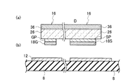
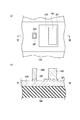
第1の実施の形態に係る半導体装置1の模式的平面パターン構成は、図1に示すように表され、図1のI−I線に沿う模式的断面構造は、図2に示すように表される。図1は、図2において、実装基板8上に配置された半導体デバイス16のドレイン電極36側から見た平面パターン構成に対応している。
[First embodiment]
(Configuration of semiconductor device)
A schematic planar pattern configuration of the
第1の実施の形態に係る半導体装置1は、図1および図2に示すように、実装基板8と、実装基板8上に配置された信号配線電極12と、実装基板8上に配置されたパワー配線電極13と、信号配線電極12と電気的に接合可能なゲートパッド電極GPおよびパワー配線電極13と電気的に接合可能なソースパッド電極SPを有する半導体デバイス16と、信号配線電極12とゲートパッド電極GPとの間に配置された第1金属粒子接合層18Gと、パワー配線電極13とソースパッド電極SPとの間に配置された第2金属粒子接合層18Sとを備える。ここで、半導体デバイス16は、実装基板8上にフリップチップ接続されている。すなわち、半導体デバイス16は、ゲートパッド電極GPおよびソースパッド電極SPが実装基板8の表面に対してフェースダウン(Face Down)に接続され、ドレイン電極36は、ゲートパッド電極GPおよびソースパッド電極SPが配置される半導体基板26の面に対向する面(実装基板8とは反対側の面)に配置される。
As shown in FIGS. 1 and 2, the
ここで、第1金属粒子接合層18Gおよび第2金属粒子接合層18Sは、導電性粒子を含むペースト材料を焼成して形成される。ペースト材料の焼成温度は、例えば、約200〜400℃である。
Here, the first metal
導電性粒子は、金属微粒子であり、例えば、銀粒子、金粒子またはニッケルや銅粒子などである。 The conductive particles are metal fine particles, such as silver particles, gold particles, nickel or copper particles.
例えば、金属微粒子として銀粒子を適用する場合、銀粒子の濃度は、例えば、約80質量%〜約95質量%である。また、銀ナノ粒子の場合の平均粒径は、約10nm〜約100nm程度である。 For example, when silver particles are applied as the metal fine particles, the concentration of the silver particles is, for example, about 80% by mass to about 95% by mass. The average particle size in the case of silver nanoparticles is about 10 nm to about 100 nm.
尚、図示は省略されているが、パワー配線電極13上の第2金属粒子接合層18Sと接する界面には、銀メッキ層を形成して、パワー配線電極13と第2金属粒子接合層18Sとの密着性をさらに確保しても良い。
Although not shown, a silver plating layer is formed on the interface of the
図2において、半導体基板26の上方にはドレイン電極36が配置されている。また、ドレイン電極36と対向する半導体基板26の表面には、ゲートパッド電極GP、ソースパッド電極SPがそれぞれ配置されている。
In FIG. 2, a
なお、特には限定されないが、ドレイン電極36、ゲートパッド電極GPおよびソースパッド電極SPは、ポリシリコン、Al、Ni等で構成される。
Although not particularly limited, the
第1の実施の形態においては、実装基板8は、絶縁体基材から成る板状のプリント基板であり、実装基板8上の所定位置にパワー配線電極13が配置されている。図2に示すように、半導体デバイス16のソースパッド電極SPと対向する位置にパワー配線電極13が配置されている。パワー配線電極13は、厚銅箔で形成される。パワー配線電極13により、低抵抗で放熱性にも優れる厚銅箔を介して、例えば、約数百アンペア程度の大電流も通電可能である。
In the first embodiment, the mounting
また、半導体デバイス16のゲートパッド電極GPと対向する実装基板8の表面には、信号配線電極12が配置されている。ここで、信号配線電極12は、例えば、銅の薄膜で形成されていても良い。この銅の薄膜の厚さは、例えば、約30〜70μmである。
A
(銀ナノペーストおよびその焼結体)
銀ナノペーストは、例えば、粒径約30nm〜約100nmの銀ナノ粒子を所定の溶媒に拡散させたものである。溶媒としては、例えばテルピネオール等の極性溶媒、テトラデカン等の炭化水素系溶媒、水系溶媒、ケトン系溶媒等が適用される。
(Silver nano paste and its sintered body)
The silver nanopaste is obtained by, for example, diffusing silver nanoparticles having a particle size of about 30 nm to about 100 nm in a predetermined solvent. As the solvent, for example, a polar solvent such as terpineol, a hydrocarbon solvent such as tetradecane, an aqueous solvent, a ketone solvent, or the like is applied.
銀ナノ粒子は、核としての銀の微粒子の表面を、有機化合物等で構成されるシェル(有機殻)で覆った構成となっている。これにより、溶媒における分散性を向上させると共に、銀の微粒子の酸化を防ぐことができる。また、焼成処理を行う前工程において、銀ナノペーストから成るペースト層を加圧して、シェルを破砕することにより、銀の微粒子の密度を高めることができ、焼結体としての金属粒子接合層の緻密性を向上させることができる。具体的な加圧の仕方については、図13を参照して後述する。 Silver nanoparticles have a structure in which the surface of fine silver particles as a nucleus is covered with a shell (organic shell) made of an organic compound or the like. Thereby, the dispersibility in the solvent can be improved and oxidation of the silver fine particles can be prevented. In addition, in the pre-process for performing the firing treatment, the density of silver fine particles can be increased by pressurizing the paste layer made of silver nanopaste and crushing the shell. Denseness can be improved. A specific method of pressurization will be described later with reference to FIG.
また、第1の実施の形態では、例えば、銀ナノ粒子の濃度が約80質量%〜約95質量%の比較的高濃度の銀ナノペーストを用いても良い。焼成によって析出される金属銀を緻密にして良好な導電性および接合性を確保するためである。 Moreover, in 1st Embodiment, you may use the comparatively high concentration silver nano paste whose density | concentration of a silver nanoparticle is about 80 mass%-about 95 mass%, for example. This is because the metallic silver deposited by firing is made dense to ensure good conductivity and bondability.
また、第1の実施の形態では、銀ナノペーストから成るペースト層の焼成温度は、例えば、約200〜400℃程度である。 Moreover, in 1st Embodiment, the baking temperature of the paste layer which consists of silver nano paste is about 200-400 degreeC, for example.
この焼成処理により、高融点の金属銀(融点約960℃)が析出して、金属粒子接合層18S、18Gを形成する。この結果、金属粒子接合層18Sを介して、ソースパッド電極SPとパワー配線電極13との間が強固に接合され、金属粒子接合層18Gを介して、ゲートパッド電極GPと信号配線電極12との間が強固に接合される。
By this firing treatment, high melting point metal silver (melting point: about 960 ° C.) is deposited to form the metal particle bonding layers 18S, 18G. As a result, the source pad electrode SP and the
しかも、この金属粒子接合層18S、18Gは、金属銀(Ag)と同等の特性を発揮することから、電気的に低抵抗(100℃で、約2.08×10⁻⁸[Ωm])で、優れた熱伝導率(300Kで、約429W/mK)を有し、上記のように融点約960℃という高い耐熱性を備えている。
Moreover, since the metal
したがって、SiCデバイスを例えば約400℃近くの高温で駆動した場合であっても、接合部が溶融することが無く、デバイス特性の信頼性、実装時の信頼性を向上することができる。 Therefore, even when the SiC device is driven at a high temperature of, for example, about 400 ° C., the junction is not melted, and the reliability of the device characteristics and the reliability at the time of mounting can be improved.
(半導体装置の製造方法)
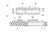
第1の実施の形態に係る半導体装置1の製造方法の一工程であって、半導体デバイス16のフリップチップ接合前の状態を示す模式的断面構造は、図3(a)に示すように表され、図3(a)に対応する実装基板8の模式的断面構造は、図3(b)に示すように表される。
(Method for manufacturing semiconductor device)
A schematic cross-sectional structure showing a state before the flip chip bonding of the
また、第1の実施の形態の変形例1に係る半導体装置1の製造方法の一工程であって、半導体デバイス16のフリップチップ接合前の状態を示す模式的断面構造は、図4(a)に示すように表され、図4(a)に対応する実装基板8の模式的断面構造は、図4(b)に示すように表される。
FIG. 4A is a schematic cross-sectional view showing a state before the flip chip bonding of the
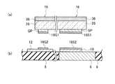
また、第1の実施の形態の変形例2に係る半導体装置1の製造方法の一工程であって、半導体デバイス16のフリップチップ接合前の状態を示す模式的断面構造は、図5(a)に示すように表され、図5(a)に対応する実装基板8の模式的断面構造は、図5(b)に示すように表される。
5A is a schematic cross-sectional view showing a state before the flip chip bonding of the
第1の実施の形態に係る半導体装置の製造方法は、図3〜図5に示すように、実装基板8上に信号配線電極12を形成する工程と、実装基板8上にパワー配線電極13を形成する工程と、信号配線電極12と電気的に接合可能なゲートパッド電極GPおよびパワー配線電極13と電気的に接合可能なソースパッド電極SPとを有する半導体デバイス16を形成する工程と、信号配線電極12もしくはゲートパッド電極GPの一方若しくは両方に第1金属粒子接合層18Gを形成する工程と、パワー配線電極13もしくはソースパッド電極SPの一方若しくは両方に第2金属粒子接合層18Sを形成する工程と、半導体デバイス16を実装基板8上にフリップチップ接続する工程とを有する。
As shown in FIGS. 3 to 5, the method of manufacturing the semiconductor device according to the first embodiment includes a step of forming a
また、第1の実施の形態に係る半導体装置の製造方法において、第1金属粒子接合層18Gを形成する工程は、導電性粒子を含むペースト層18を信号配線電極12もしくはゲートパッド電極GPの一方若しくは両方に塗布する工程を有し、第2金属粒子接合層18Sを形成する工程は、導電性粒子を含むペースト層18をパワー配線電極13もしくはソースパッド電極SPの一方若しくは両方に塗布する工程を有する。
Further, in the method of manufacturing the semiconductor device according to the first embodiment, the step of forming the first metal
また、第1の実施の形態に係る半導体装置の製造方法において、半導体デバイス16を実装基板8上にフリップチップ接続する工程は、ペースト層18を介して信号配線電極12とゲートパッド電極GPとを当接させ、当接状態においてペースト層18を所定温度で焼成し、信号配線電極12とゲートパッド電極GPとを接合する工程と、ペースト層18を介してパワー配線電極13とソースパッド電極SPとを当接させ、当接状態においてペースト層18を所定温度で焼成し、パワー配線電極13とソースパッド電極SPとを接合する工程とを有する。
In the method of manufacturing the semiconductor device according to the first embodiment, the step of flip-chip connecting the
第1の実施の形態においては、図3に示すように、実装基板8側に金属粒子接合層18G、18Sが配置されている。より具体的には、パワー配線電極13の表面上に、金属粒子接合層18Sが設けられ、信号配線電極12の表面上に、金属粒子接合層18Gが配置されている。
In the first embodiment, as shown in FIG. 3, metal
第1の実施の形態の変形例1においては、図4に示すように、半導体デバイス16側に金属粒子接合層18G、18Sが配置されている。より具体的には、ソースパッド電極SPの上に金属粒子接合層18Sが配置され、ゲートパッド電極GPの上に金属粒子接合層18Gが配置されている。
In
第1の実施の形態の変形例2においては、図5に示すように、半導体デバイス16および実装基板8の両側に金属粒子接合層18G1、18G2、18S1および18S2がそれぞれ配置されている。より具体的には、ソースパッド電極SP上に金属粒子接合層18S1が配置され、ゲートパッド電極GP上に金属粒子接合層18G1が配置され、パワー配線電極13上に、金属粒子接合層18S2が配置され、信号配線電極12上に金属粒子接合層18G2が配置されている。なお、18G1と18G2、18G2と18S1が密着された状態で焼成されて形成される金属粒子接合層の厚さを勘案して、18G1、18G2、18S1および18S2の厚さは、それぞれ約5μm〜約50μm程度とされる。
In the second modification of the first embodiment, as shown in FIG. 5, metal particle bonding layers 18G1, 18G2, 18S1, and 18S2 are disposed on both sides of the
第1の実施の形態に係る半導体装置の製造方法の一工程において、塗布された金属粒子接合層として銀ナノペーストを加圧する前の状態は、図13(a)に示すように模式的に表され、加圧後の銀ナノペーストの状態は、図13(b)に示すように模式的に表される。 In one step of the method for manufacturing the semiconductor device according to the first embodiment, the state before pressurizing the silver nanopaste as the applied metal particle bonding layer is schematically represented as shown in FIG. The state of the silver nanopaste after pressurization is schematically represented as shown in FIG.
図13(a)において、各銀ナノ粒子22は、有機化合物等で構成されるシェル(有機殻)20aで被覆された形態で、例えば、テルピネオール等の溶媒20中において拡散した状態となっている。
In FIG. 13A, each
この状態からペースト層18を上下方向から圧力Pを加えて圧縮すると、図13(b)に示す状態に変化する。即ち、有機化合物等で構成されるシェル20aが加圧によって破砕され、各銀ナノ粒子22が密着した状態となる。これにより、ペースト層18の厚さは、L1からL2に縮まった状態となる。
When the
金属粒子接合層18G、18Sを形成するペースト層18の塗布には、後述するマスク25およびスキージ(ヘラ部材)27を用いたスクリーン印刷の手法が適用される。
For the application of the
また、ペースト層18の厚さは、例えば約10μm〜約50μmとされる。なお、金属粒子接合層18G、18Sの厚さは、焼成時の収縮によりペースト層18の厚さの半分程度となる。即ち、例えばペースト層18の厚さが約50μmの場合に、焼成後の金属粒子接合層18G、18Sの厚さは約20μm〜約30μm程度となることが実験により確認されている。
Further, the thickness of the
(加圧および加熱工程)
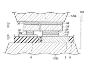
第1の実施の形態に係る半導体装置の製造方法の一工程であって、加圧工程を示す模式的断面構造は、図6に示すように表される。
(Pressurization and heating process)
A schematic cross-sectional structure showing a pressurizing process, which is a process of the method for manufacturing the semiconductor device according to the first embodiment, is expressed as shown in FIG.
第1の実施の形態若しくは変形例1〜2において、図6に示すように、金属粒子接合層18G・18S(加熱・加圧前は、ペースト層18)を挟んで、実装基板8上に半導体デバイス16をフェースダウン状態で位置合わせして載置し、その状態で、プレス加工機120(120a、120b)にセットして矢印P方向に圧力を加える。
In the first embodiment or the modified examples 1 and 2, as shown in FIG. 6, a semiconductor is mounted on the mounting
この際の圧力は、例えば、約2MPa〜約30MPaとされる。これにより、ペースト層18は、図13(a)の状態から図13(b)のように、各銀ナノ粒子22が密着した状態となる。
The pressure at this time is, for example, about 2 MPa to about 30 MPa. Thereby, the
尚、上記の加圧工程では、加圧と加熱を同時に行うために、図示は省略するが、所定のベーキング装置などによって半導体装置全体を約200℃〜約400℃で所定時間にわたって加熱する。 In the above pressurization step, since the pressurization and heating are performed simultaneously, although not shown, the entire semiconductor device is heated at about 200 ° C. to about 400 ° C. for a predetermined time by a predetermined baking apparatus or the like.
これにより、ペースト層18が焼成され、金属銀が析出して金属粒子接合層18G・18Sが形成される。
Thereby, the
この金属銀から成る金属粒子接合層18G・18Sは、ゲートパッド電極GP・信号配線電極12間、およびソースパッド電極SP・パワー配線電極13間を強固に接合し、実装基板8の上に半導体デバイス16がフェースダウン状態で電気的に接合される。
The metal
第1の実施の形態およびその変形例1〜2によれば、銀ナノペーストを塗布して焼成するという簡易な工程により高い耐熱性を備えたワイヤレス接合を形成することができる。 According to 1st Embodiment and its modifications 1-2, the wireless joining provided with high heat resistance can be formed by the simple process of apply | coating and baking silver nano paste.
また、第1の実施の形態およびその変形例1〜2によれば、銀ナノペーストの焼結体である金属銀によって金属粒子接合層を形成することにより、金属粒子接合層の耐熱性、熱伝導性等を高めることができ、SiC系FET、GaN系FETなどの半導体デバイス等に適した半導体装置を提供することができる。 Moreover, according to 1st Embodiment and its modifications 1-2, heat resistance of a metal particle joining layer, heat | fever are formed by forming a metal particle joining layer with the metallic silver which is a sintered compact of silver nanopaste. Conductivity can be increased, and a semiconductor device suitable for a semiconductor device such as a SiC-based FET or a GaN-based FET can be provided.
また、第1の実施の形態およびその変形例1〜2によれば、金属粒子接合層は金属銀で形成され、鉛(Pb)を用いることが無いので、鉛フリーとなり公害対策に資することができる。 Moreover, according to 1st Embodiment and its modifications 1-2, a metal particle joining layer is formed with metal silver, and since lead (Pb) is not used, it becomes lead-free and contributes to pollution measures. it can.
第1の実施の形態およびその変形例1〜2によれば、低コストで高い耐熱性ワイヤレスを有する半導体装置およびその製造方法を提供することができる。 According to 1st Embodiment and its modifications 1-2, the semiconductor device which has low heat and high heat-resistant wireless, and its manufacturing method can be provided.
[第2の実施の形態]
(半導体装置の構成)
第2の実施の形態に係る半導体装置1の模式的平面パターン構成は、図7に示すように表され、図7のII−II線に沿う模式的断面構造は、図8に示すように表される。図7は、図8において、実装基板8上に配置された半導体デバイス16のドレイン電極36側から見た平面パターン構成に対応している。
[Second Embodiment]
(Configuration of semiconductor device)
A schematic planar pattern configuration of the
第2の実施の形態に係る半導体装置1は、図7および図8に示すように、実装基板8と、実装基板8上に配置された信号配線電極12と、実装基板8を貫通して配置されたパワー配線電極6と、信号配線電極12と電気的に接合可能なゲートパッド電極GPおよびパワー配線電極6と電気的に接合可能なソースパッド電極SPを有する半導体デバイス16と、信号配線電極12とゲートパッド電極GPとの間に配置された第1金属粒子接合層18Gと、パワー配線電極6とソースパッド電極SPとの間に配置された第2金属粒子接合層18Sとを備える。ここで、半導体デバイス16は、実装基板8上にフリップチップ接続されている。すなわち、半導体デバイス16は、ゲートパッド電極GPおよびソースパッド電極SPが実装基板8の表面に対してフェースダウン(Face Down)に接続され、ドレイン電極36は、ゲートパッド電極GPおよびソースパッド電極SPが配置される半導体基板26の面に対向する面(実装基板8とは反対側の面)に配置される。
As shown in FIGS. 7 and 8, the
第2の実施の形態においては、実装基板8を貫通して配置されたパワー配線電極6を備えることによって、第1の実施の形態に比べ、さらに大電流の半導体デバイス16を実装基板8上に搭載可能である。
In the second embodiment, by providing the
ここで、第1金属粒子接合層18Gおよび第2金属粒子接合層18Sは、導電性粒子を含むペースト材料を焼成して形成される。ペースト材料の焼成温度は、例えば、約200〜400℃である。
Here, the first metal
導電性粒子は、金属微粒子であり、例えば、銀粒子、金粒子、銅粒子またはニッケル粒子のいずれかである。 The conductive particles are metal fine particles, for example, silver particles, gold particles, copper particles, or nickel particles.
例えば、金属微粒子として銀ナノ粒子を適用する場合、銀ナノ粒子の濃度は、例えば、約80質量%〜約95質量%である。また、銀ナノ粒子の粒径は、約10nm〜約100nmである。 For example, when silver nanoparticles are applied as the metal fine particles, the concentration of silver nanoparticles is, for example, about 80% by mass to about 95% by mass. The silver nanoparticles have a particle size of about 10 nm to about 100 nm.
第2の実施の形態においては、実装基板8は、絶縁体基材から成る板状のプリント基板であり、実装基板8の所定位置にパワー配線電極6が埋め込まれた構成を有する。図8に示すように、半導体デバイス16のソースパッド電極SPと対向する位置にパワー配線電極6が埋め込まれている。パワー配線電極6は、例えば、厚さ0.5〜1.0mm程度の厚銅板で形成される。パワー配線電極6により、低抵抗で放熱性にも優れる厚銅板を介して、例えば、約数百アンペア程度の大電流も実装基板8の厚さ方向及び平面方向への通電が可能である。
In the second embodiment, the mounting
なお、第2金属粒子接合層18Sとして、例えば、銀ナノペーストから成るペースト層およびその焼結体を適用する場合には、第2金属粒子接合層18Sとの接合性を向上させるために、ソースパッド電極SPと対向するパワー配線電極6の表面に、銀メッキ層19が形成されていても良い。
As the second metal
第2の実施の形態に係る半導体装置1においては、銀メッキ層19とソースパッド電極SPとの間および信号配線電極12とゲートパッド電極GPとの間には、金属ナノペーストとして、例えば、銀ナノペーストを焼成して得られる金属粒子接合層18S、18Gがそれぞれ配置されている。
In the
この金属粒子接合層18S、18Gを介して、銀メッキ層19とソースパッド電極SPとの間および信号配線電極12とゲートパッド電極GPとの間を電気的に接合している。
The
また、半導体デバイス16のゲートパッド電極GPと対向する実装基板8の表面には、信号配線電極12が配置されている。ここで、信号配線電極12は、例えば、銅の薄膜で形成されていても良い。この銅の薄膜の厚さは、例えば、約15〜約70μmである。
A
第2の実施の形態に係る半導体装置1において適用可能な銀ナノペーストおよびその焼結体については、第1の実施の形態と同様であるため、重複説明は省略する。
The silver nanopaste and its sintered body that can be applied in the
(半導体装置の製造方法)
第2の実施の形態に係る半導体装置1の製造方法の一工程であって、半導体デバイス16のフリップチップ接合前の状態を示す模式的断面構造は、図9(a)に示すように表され、図9(a)に対応する実装基板8の模式的断面構造は、図9(b)に示すように表される。
(Method for manufacturing semiconductor device)
A schematic cross-sectional structure showing a state before the flip chip bonding of the
また、第2の実施の形態の変形例1に係る半導体装置1の製造方法の一工程であって、半導体デバイス16のフリップチップ接合前の状態を示す模式的断面構造は、図10(a)に示すように表され、図10(a)に対応する実装基板8の模式的断面構造は、図10(b)に示すように表される。
10A is a schematic cross-sectional view showing a state before the flip chip bonding of the
また、第2の実施の形態の変形例2に係る半導体装置1の製造方法の一工程であって、半導体デバイス16のフリップチップ接合前の状態を示す模式的断面構造は、図11(a)に示すように表され、図11(a)に対応する実装基板8の模式的断面構造は、図11(b)に示すように表される。
Further, a schematic cross-sectional structure showing a state before the flip chip bonding of the
第2の実施の形態に係る半導体装置の製造方法は、図9〜図11に示すように、実装基板8上に信号配線電極12を形成する工程と、実装基板8を貫通してパワー配線電極6を形成する工程と、信号配線電極12と電気的に接合可能なゲートパッド電極GPおよびパワー配線電極6と電気的に接合可能なソースパッド電極SPとを有する半導体デバイス16を形成する工程と、信号配線電極12もしくはゲートパッド電極GPの一方若しくは両方に第1金属粒子接合層18Gを形成する工程と、パワー配線電極6もしくはソースパッド電極SPの一方若しくは両方に第2金属粒子接合層18Sを形成する工程と、半導体デバイス16を実装基板8上にフリップチップ接続する工程とを有する。
As shown in FIGS. 9 to 11, the method for manufacturing a semiconductor device according to the second embodiment includes a step of forming a
また、第2の実施の形態に係る半導体装置の製造方法において、第1金属粒子接合層18Gを形成する工程は、導電性粒子を含むペースト層18を信号配線電極12もしくはゲートパッド電極GPの一方若しくは両方に塗布する工程を有し、第2金属粒子接合層18Sを形成する工程は、導電性粒子を含むペースト層18をパワー配線電極6もしくはソースパッド電極SPの一方若しくは両方に塗布する工程を有する。
Further, in the method of manufacturing the semiconductor device according to the second embodiment, the step of forming the first metal
また、第2の実施の形態に係る半導体装置の製造方法において、半導体デバイス16を実装基板8上にフリップチップ接続する工程は、ペースト層18を介して信号配線電極12とゲートパッド電極GPとを当接させ、当接状態においてペースト層18を所定温度で焼成し、信号配線電極12とゲートパッド電極GPとを接合する工程と、ペースト層18を介してパワー配線電極6とソースパッド電極SPとを当接させ、当接状態においてペースト層18を所定温度で焼成し、パワー配線電極6とソースパッド電極SPとを接合する工程とを有する。
In the method of manufacturing a semiconductor device according to the second embodiment, the step of flip-chip connecting the
第2の実施の形態においては、図9に示すように、実装基板8側に金属粒子接合層18G、18Sが配置されている。より具体的には、パワー配線電極13の表面上に、金属粒子接合層18Sが設けられ、信号配線電極12の表面上に、金属粒子接合層18Gが配置されている。
In the second embodiment, as shown in FIG. 9, metal
第2の実施の形態の変形例1においては、図10に示すように、半導体デバイス16側に金属粒子接合層18G、18Sが配置されている。より具体的には、ソースパッド電極SPの上に金属粒子接合層18Sが配置され、ゲートパッド電極GPの上に金属粒子接合層18Gが配置されている。
In
第2の実施の形態の変形例2においては、図11に示すように、半導体デバイス16および実装基板8の両側に金属粒子接合層18G1、18G2、18S1および18S2がそれぞれ配置されている。より具体的には、ソースパッド電極SP上に金属粒子接合層18S1が配置され、ゲートパッド電極GP上に金属粒子接合層18G1が配置され、パワー配線電極6上に、金属粒子接合層18S2が配置され、信号配線電極12上に金属粒子接合層18G2が配置されている。なお、18G1と18G2、18G2と18S1が密着された状態で焼成されて形成される金属粒子接合層の厚さを勘案して、18G1、18G2、18S1および18S2の厚さは、それぞれ5〜25μm程度とされる。
In
第2の実施の形態に係る半導体装置の製造方法の一工程において、塗布された金属粒子接合層として銀ナノペーストを加圧する前の状態は、図13(a)に示すように表され、加圧後の銀ナノペーストの状態は、図13(b)に示すように表される。その他の説明は、第1の実施の形態と同様であるため、重複説明は省略する。 In one step of the method of manufacturing the semiconductor device according to the second embodiment, the state before pressurizing the silver nanopaste as the applied metal particle bonding layer is expressed as shown in FIG. The state of the silver nanopaste after pressing is expressed as shown in FIG. Since other explanations are the same as those in the first embodiment, duplicate explanations are omitted.
(加圧および加熱工程)
第2の実施の形態に係る半導体装置の製造方法の一工程であって、加圧工程を示す模式的断面構造は、図12に示すように表される。
(Pressurization and heating process)
A schematic cross-sectional structure showing a pressurizing step, which is one step of the method of manufacturing a semiconductor device according to the second embodiment, is expressed as shown in FIG.
第2の実施の形態若しくは変形例1〜2において、図12に示すように、金属粒子接合層18G・18S(加熱・加圧前は、ペースト層18)を挟んで、実装基板8上に半導体デバイス16をフェースダウン状態で位置合わせして載置し、その状態で、プレス加工機120(120a、120b)にセットして矢印P方向に圧力を加える。
In the second embodiment or the modified examples 1 and 2, as shown in FIG. 12, a semiconductor is mounted on the mounting
この際の圧力は、例えば、約2MPa〜約30MPaとされる。これにより、ペースト層18は、図13(a)の状態から図13(b)のように、各金属粒子22が密着した状態となる。
The pressure at this time is, for example, about 2 MPa to about 30 MPa. As a result, the
尚、上記の加圧工程では、加圧と加熱を同時に行うために、図示は省略するが、所定のベーキング装置などによって半導体装置全体を200〜400℃で所定時間にわたって加熱する。 In the pressurization step, since the pressurization and heating are performed simultaneously, the entire semiconductor device is heated at 200 to 400 ° C. for a predetermined time by a predetermined baking apparatus or the like (not shown).
これにより、ペースト層18が焼成され、金属銀が析出して金属粒子接合層18G・18Sが形成される。
Thereby, the
この金属銀から成る金属粒子接合層18G・18Sは、ゲートパッド電極GP・信号配線電極12間、およびソースパッド電極SP・パワー配線電極13間を強固に接合し、実装基板8の上に半導体デバイス16がフェースダウン状態で電気的に接合される。
The metal
第2の実施の形態およびその変形例1〜2によれば、低コストで高い耐熱性を有する半導体装置およびその製造方法を提供することができる。 According to 2nd Embodiment and its modifications 1-2, the semiconductor device which has high heat resistance at low cost, and its manufacturing method can be provided.
(半導体装置を適用した応用例)
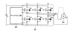
次に、図14を参照して、第1〜第2の実施の形態に係る半導体装置1を用いて構成した3相インバータについて説明する。
(Application examples using semiconductor devices)
Next, a three-phase inverter configured using the
図14に示すように、3相インバータは、ゲートドライブ部50と、ゲートドライブ部50に接続されたパワーモジュール部52と、3相モータ部54とを備える。パワーモジュール部52は、3相モータ部54のU相、V相、W相に対応して、U、V、W相のインバータが接続されている。
As shown in FIG. 14, the three-phase inverter includes a
パワーモジュール部52は、コンデンサCが接続されたプラス端子(+)とマイナス端子(−)間に、インバータ構成のSiC・MOSFETQ1・Q2、Q3・Q4、およびQ5・Q6が接続されている。さらに、SiC・MOSFETQ1〜Q6のソース・ドレイン間には、ダイオードD1〜D6がそれぞれ逆並列に接続されている。
In the
第1〜第2の実施の形態に係る半導体装置1に適用される半導体デバイス16に相当するSiC・MOSFETQ1〜Q6は、上述のように、金属粒子接合層18S・18Gを介して実装基板8の上にフリップチップ構成に電気的に接続される。
As described above, the SiC MOSFETs Q1 to Q6 corresponding to the
(半導体デバイスの構成例)
第1〜第2の実施の形態に係る半導体装置1に適用する半導体デバイス16の例として、SiC・MOSFETの模式的断面構造は、図15に示すように、n−高抵抗層からなる半導体基板26と、半導体基板26の表面側に形成されたpベース領域28と、pベース領域28の表面に形成されたソース領域30と、pベース領域28間の半導体基板26の表面上に配置されたゲート絶縁膜32と、ゲート絶縁膜32上に配置されたゲート電極38と、ソース領域30に接続されたソース電極34と、半導体基板26の表面と反対側の裏面に配置されたn+ドレイン領域24と、n+ドレイン領域24に接続されたドレイン電極36とを備える。
(Configuration example of semiconductor device)
As an example of the
図15では、半導体デバイス16は、プレーナゲート型nチャネル縦型SiC・MOSFETで構成されているが、トレンチゲート型nチャネル縦型SiC・MOSFETなどで構成されていても良い。
In FIG. 15, the
また、第1〜第2の実施の形態に係る半導体装置1に適用する半導体デバイス16には、SiC・MOSFETの代わりに、GaN系FETなどを適用することもできる。
Further, a GaN-based FET or the like can be applied to the
更には、第1〜第2の実施の形態に係る半導体装置1に適用する半導体デバイス16には、バンドギャップエネルギーが、例えば、1.1eV〜8eVの半導体を用いることができる。
Furthermore, the
第1〜第2の実施の形態に係る半導体装置によれば、金属粒子ペースト層を焼成して形成される金属粒子接合層18G・18Sとして、例えば、金属銀の融点が約960℃と高い耐熱性を備えているため、この金属粒子接合層18G・18SをSiC系FETやGaN系FETなどのパワーデバイスに適用することによって、パワーデバイスを高温で駆動することができる。
According to the semiconductor device according to the first to second embodiments, as the metal
第1〜第2の実施の形態に係るに適用する半導体デバイス16の例であって、ソースパッド電極SP、ゲートパッド電極GPを含むSiC・MOSFETの模式的断面構造は、図16に示すように表される。ゲートパッド電極GPは、ゲート絶縁膜32上に配置されたゲート電極38に接続され、ソースパッド電極SPは、ソース領域30に接続されたソース電極34に接続される。
FIG. 16 shows an example of the
また、ゲートパッド電極GPおよびソースパッド電極SPは、図16に示すように、半導体デバイス16の表面を覆うパッシべーション用の層間絶縁膜44上に配置される。尚、ゲートパッド電極GPおよびソースパッド電極SPの下方の半導体基板26内には、図16の構成例では、図示を省略しているが、図15或いは、図16の中央部と同様に、微細構造のトランジスタ構造が形成されていても良い。
Further, as shown in FIG. 16, the gate pad electrode GP and the source pad electrode SP are disposed on an
さらに、図16の構成例では、図示を省略しているが、図16の中央部のトランジスタ構造においても、パッシべーション用の層間絶縁膜44上にソースパッド電極SP若しくはゲートパッド電極GPが延在して配置されていても良い。
Further, although not shown in the configuration example of FIG. 16, the source pad electrode SP or the gate pad electrode GP extends on the passivation
さらに、実装時には、半導体デバイス16がフェースダウンされ、ゲートパッド電極GP・ソースパッド電極SPが、図2若しくは図8に示すように、それぞれ金属粒子接合層18G・18Sを介して実装基板8に接合される。
Further, at the time of mounting, the
(ペースト層塗布工程)
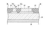
第1〜第2の実施の形態に係る半導体装置の製造方法の一工程であって、半導体基板26上にペースト層18を塗布するためのマスク25を配置した状態を示す模式的平面パターン構成は、図17(a)に示すように表され、図17(a)のIII−III線に沿う模式的断面構造は、図17(b)に示すように表される。
(Paste layer application process)
A schematic planar pattern configuration showing a state in which a
第1〜第2の実施の形態に係る半導体装置の製造方法の一工程であって、開口部25aを有するマスク25上にペースト層18を堆積した状態を示す模式的断面構造は、図18に示すように表される。
FIG. 18 shows a schematic cross-sectional structure showing a state where the
第1〜第2の実施の形態に係る半導体装置の製造方法の一工程であって、スキージ27を矢印A方向に移動させてペースト層18をマスク25の開口部25aに充填する工程を示す模式的断面構造は、図19に示すように表される。
Schematic showing one step of the method of manufacturing a semiconductor device according to the first to second embodiments, the step of filling the
第1〜第2の実施の形態に係る半導体装置の製造方法の一工程であって、マスク25の開口部25aにペースト層18が充填された状態を示す模式的断面構造は、図20に示すように表される。
A schematic cross-sectional structure showing a state in which the
第1〜第2の実施の形態に係る半導体装置の製造方法において、ペースト層18を信号配線電極12もしくはゲートパッド電極GPの一方に塗布する工程は、信号配線電極12もしくはゲートパッド電極GPの一方に、各電極位置に合わせた開口部25aを有するマスク25を位置合わせして重ね合わせる工程と、マスク25の上にペースト層18を堆積する工程と、スキージ27によってペースト層18を開口部25aに充填する工程と、マスク25を取り除く工程とを有する。
In the method of manufacturing a semiconductor device according to the first to second embodiments, the step of applying the
また、第1〜第2の実施の形態に係る半導体装置の製造方法において、ペースト層18をパワー配線電極6・13もしくはソースパッド電極SPの一方に塗布する工程は、パワー配線電極6・13もしくはソースパッド電極SPの一方に、各電極位置に合わせた開口部25aを有するマスク25を位置合わせして重ね合わせる工程と、マスク25の上にペースト層18を堆積する工程と、スキージ27によってペースト層18を開口部25aに充填する工程と、マスク25を取り除く工程とを有する。
In the method for manufacturing a semiconductor device according to the first to second embodiments, the step of applying the
以下、ペースト層塗布工程を詳述する。 Hereinafter, the paste layer application step will be described in detail.
(a)まず、図17(a)および図17(b)に示すように、半導体デバイス16のゲートパッド電極GPおよびソースパッド電極SPを含む部位にマスク(例えば、金属製のマスク)25を重ね合わせ、マスク25の開口部25aを介してゲートパッド電極GPおよびソースパッド電極SPの所定の領域のみが露出するようにする。なお、ゲートパッド電極GPおよびソースパッド電極SPの表面からマスク25の表面までの距離が、形成するペースト層18の厚さと等しい値、例えば、約10μm〜約100μm程度となるように、マスク25の厚さが設定される。
(A) First, as shown in FIGS. 17A and 17B, a mask (for example, a metal mask) 25 is overlaid on a portion of the
(b)次に、図18に示すように、所定の量の金属微粒子ペーストからなるペースト層18をキャピラリやディスペンサなどを用いて、マスク25および開口部25a上に堆積する。
(B) Next, as shown in FIG. 18, a
(c)次に、図19に示すように、スキージ(ヘラ部材)27の先端部をマスク25の表面に当接させ、矢印A方向(図19上では左側から右側)に移動させて、余分なペースト層18を除去すると共に、マスク25の開口部25a内にペースト層18を充填させる。
(C) Next, as shown in FIG. 19, the tip of the squeegee (spatial member) 27 is brought into contact with the surface of the
結果として、図20に示すように、マスク25の開口部25aの内壁に沿って、ゲートパッド電極GP上およびソースパッド電極SP上にペースト層18がそれぞれ形成される。
As a result, as shown in FIG. 20, the paste layers 18 are formed on the gate pad electrode GP and the source pad electrode SP along the inner wall of the
そして、この後、マスク25を半導体デバイス16側から取り外し、半導体デバイス16をフェースダウン状態として、実装基板8との接合工程に移行する(図4若しくは図10参照)。
Then, after that, the
なお、ペースト層18の粘度等の性質に応じて、図20の状態で所定時間にわたって乾燥させ、ペースト層18を半乾きの状態としてからマスク25を取り外した方が良い場合もある。この乾燥工程では、自然乾燥であって、或いは、所定温度で昇温加熱工程を実施しても良い。
Depending on properties such as the viscosity of the
また、図17〜図20の例では、半導体デバイス16側にペースト層18を塗布する工程について説明したが、同様の手法で、実装基板8上の信号配線電極12やパワー配線電極13・6上にペースト層18を形成することもできる(図3(b)若しくは図9(b)参照)。
In the example of FIGS. 17 to 20, the process of applying the
また、図5若しくは図11に示すように、同様の手法で、半導体デバイス16側と実装基板8側の両方にペースト層18を形成し、18G1と18G2、18S1と18S2とを対向させて接合することもできる。この際に、18G1、18G2側および18S1、18S2側の少なくとも一方については、所定時間にわたって乾燥させて半乾きの状態とした方が、より良好に接合できる。
Also, as shown in FIG. 5 or FIG. 11, the
第2の実施の形態およびその変形例1〜2によれば、金属微粒子ペーストを塗布して焼成するという簡易な工程により高い耐熱性を備えたワイヤレス接合を形成することができる。 According to 2nd Embodiment and its modifications 1-2, the wireless joining provided with high heat resistance can be formed by the simple process of apply | coating and baking a metal fine particle paste.
また、第2の実施の形態およびその変形例1〜2によれば、金属微粒子ペーストの焼結体である金属によって接合層を形成することにより、金属粒子接合層の耐熱性、熱伝導性等を高めることができ、SiC系FET、GaN系FETなどの半導体デバイス等に適した半導体装置を提供することができる。 Moreover, according to 2nd Embodiment and its modifications 1-2, by forming a joining layer with the metal which is a sintered compact of metal fine particle paste, the heat resistance of the metal particle joining layer, thermal conductivity, etc. A semiconductor device suitable for semiconductor devices such as SiC-based FETs and GaN-based FETs can be provided.
また、第2の実施の形態およびその変形例1〜2によれば、金属接合層は銀、金、銅またはニッケルで形成され、鉛(Pb)を用いることが無いので、鉛フリーとなり公害対策に資することができる。 Further, according to the second embodiment and the first and second modifications thereof, the metal bonding layer is formed of silver, gold, copper or nickel and does not use lead (Pb). Can help.
第2の実施の形態およびその変形例1〜2によれば、低コストで高い耐熱性ワイヤレス接合を有する半導体装置およびその製造方法を提供することができる。 According to the second embodiment and the first and second modifications thereof, it is possible to provide a semiconductor device having a high heat-resistant wireless junction at low cost and a method for manufacturing the same.
また、第2の実施の形態およびその変形例1〜2によれば、実装基板を貫通して配置されたパワー配線電極を備えるため、第1の実施の形態に比べ、さらに大電流の半導体デバイスを実装基板上に搭載可能である。 In addition, according to the second embodiment and the first and second modifications thereof, since the power wiring electrode disposed through the mounting substrate is provided, a semiconductor device having a larger current than that of the first embodiment. Can be mounted on a mounting board.
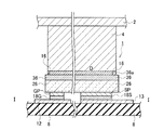
さらに、第1〜第2の実施の形態に係る半導体装置においては、図21〜図22に示すように、ドレイン電極36上に半田などのドレイン電極接合層36aを介して柱状電極4を配置しても良い。柱状電極4は、例えば、銅モリブデン(CuMo)などのSiCと相対的に線膨張係数の値の近い金属材料を選択する。ドレイン電極接合層36aは、金属粒子接合層18S・18Gと同様の導電性粒子を含むペースト材料を焼成して形成しても良い。ペースト材料の焼成温度は、例えば、約200〜400℃である。導電性粒子は、金属微粒子であり、例えば、銀粒子、金粒子またはニッケルや銅粒子などである。
Furthermore, in the semiconductor device according to the first to second embodiments, as shown in FIGS. 21 to 22, the
柱状電極4上には、さらにヒートスプレッダー2が配置される。さらに、実装基板8を搭載するヒートスプレッダーを配置することで、第1〜第2の実施の形態に係る半導体装置においては、両面冷却を実施可能である。
A
[比較例]
図23〜図25を参照して、比較例について簡単に説明する。
[Comparative example]
A comparative example will be briefly described with reference to FIGS.
図23に示す比較例は、絶縁基板100上に形成された半導体デバイス140のソースパッド電極SPの上に柱状電極180を形成すると共に、ゲートパッド電極GPについては橋状のリード部材160を介して配線部125との接合を図った構成を示す。
In the comparative example shown in FIG. 23, the
この構成では、従来のワイヤボンディングを行わなくて良いという利点がある反面、リード部材160自体が微細部品であり、マウントが難しいという問題がある。
This configuration has the advantage that the conventional wire bonding need not be performed, but has the problem that the
また、リード部材160自体が比較的高価であるため、コストが嵩むという不都合もある。
Further, since the
また、半導体デバイス140側と配線部125側とに高低差を生じた場合には、図23の(b)に示すようにリード部材160の端部が浮いてしまい、接続不良を生じるという難点もある。
Further, when there is a difference in height between the
図22に示す比較例は、絶縁基板100上に形成された半導体デバイス140のソースパッド電極SPの上に柱状電極180を形成すると共に、ゲートパッド電極GPについては銀ナノペーストの焼結体18Aを介して配線部125との接合を図った構成を示す。
In the comparative example shown in FIG. 22, the
この構成では、従来のワイヤボンディングを行わなくても良く、また図23の比較例のように配線部品を用いなくても良いという利点がある。 This configuration has the advantage that conventional wire bonding does not have to be performed, and wiring components need not be used as in the comparative example of FIG.
しかしながら、銀ナノペーストの焼結体18Aと半導体デバイス140の側面や、銀ナノペーストの焼結体18Aの下方の絶縁性確保が難しいという問題がある。
However, there is a problem that it is difficult to ensure the insulating properties of the side surfaces of the silver nanopaste sintered
図25に示す比較例は、絶縁基板100上に形成された半導体デバイス140のソースパッド電極SPの上に柱状電極180を、ゲートパッド電極GPの上に柱状電極200をそれぞれ形成し、柱状電極180および柱状電極200の上部端面を介して絶縁基板100と対向する実装基板(図示省略)等との接合を図る構成を示す。
In the comparative example shown in FIG. 25, the
しかしながら、微細加工の柱状電極が必要であり、特に約500μm角以下の柱状電極を形成することが難しいという問題がある。 However, there is a problem that a finely processed columnar electrode is necessary, and it is difficult to form a columnar electrode having a size of about 500 μm square or less.
また、柱状電極を用いる場合には、垂直方向の配線に限定され、水平方向の配線には適用できないという不都合もある。 Further, when the columnar electrode is used, it is limited to the wiring in the vertical direction, and there is a disadvantage that it cannot be applied to the wiring in the horizontal direction.
また、柱状電極180および柱状電極200の上部端面と実装基板等との接合を半田を介して行う場合には、高耐熱接合技術の応用が困難であり、SiCデバイス等の高温での動作に対応できないという不都合もある。
In addition, when the upper end surfaces of the
本実施の形態によれば、低コストで高い耐熱性を有する半導体装置の実装構造を提供することができる。 According to the present embodiment, it is possible to provide a mounting structure of a semiconductor device having high heat resistance at low cost.
また、本実施の形態によれば、簡易な工程により高い耐熱性を有するワイヤレス接合を実施可能な半導体装置の実装方法を提供することができる。 Further, according to the present embodiment, it is possible to provide a semiconductor device mounting method capable of performing wireless bonding having high heat resistance by a simple process.
[その他の実施の形態]
上記のように、実施の形態および変形例によって記載したが、この開示の一部をなす論述および図面は例示的なものであり、この発明を限定するものであると理解すべきではない。この開示から当業者には様々な代替実施の形態、実施例および運用技術が明らかとなろう。
[Other embodiments]
As described above, the embodiments and modifications have been described. However, the descriptions and drawings forming a part of this disclosure are illustrative and should not be understood as limiting the present invention. From this disclosure, various alternative embodiments, examples and operational techniques will be apparent to those skilled in the art.
このように、本発明はここでは記載していない様々な実施の形態などを含む。 As described above, the present invention includes various embodiments not described herein.
例えば、上記実施の形態では、導電性粒子を含むペースト材料として銀ナノペーストを用いる場合について説明したが、これに限定されず、金ナノ粒子またはニッケルナノ粒子を所定の溶媒に分散させた金属ナノ粒子ペーストを用いるようにしてもよい。 For example, in the above embodiment, the case where silver nanopaste is used as a paste material containing conductive particles has been described. However, the present invention is not limited to this, and metal nanoparticles in which gold nanoparticles or nickel nanoparticles are dispersed in a predetermined solvent are described. A particle paste may be used.
本発明の半導体装置は、パワー半導体モジュール、インテリジェントパワーモジュールなどパワーデバイス全般に利用可能である。 The semiconductor device of the present invention can be used for all power devices such as a power semiconductor module and an intelligent power module.
1…半導体装置
2…ヒートスプレッダー
4…柱状電極
6、13…パワー配線電極
8…実装基板
12…信号配線電極
16…半導体デバイス
18…ペースト層
18G、18S…金属粒子接合層
19…銀メッキ層
20…溶媒
20a…シェル
22…銀ナノ粒子
24…n+ドレイン領域
25…マスク
25a…開口部
26…半導体基板
27…スキージ(ヘラ部材)
28…pベース領域
30…ソース領域
32…ゲート絶縁膜
34…ソース電極
36…ドレイン電極
36a…ドレイン電極接合層
38…ゲート電極
44…層間絶縁膜
50…ゲートドライブ部
52…パワーモジュール部
54…三相モータ部
120…プレス加工機
C…コンデンサ
D1〜D6…ダイオード
GP…ゲートパッド電極
SP…ソースパッド電極
DESCRIPTION OF
28 ...
Claims (26)
前記実装基板上に配置された信号配線電極と、
前記実装基板上若しくは前記実装基板を貫通して配置されたパワー配線電極と、
前記信号配線電極と電気的に接合可能なゲートパッド電極と、前記パワー配線電極と電気的に接合可能なソースパッド電極とを有するパワーデバイスと、
前記信号配線電極と前記ゲートパッド電極との間に配置され、複数の金属微粒子と前記複数の金属微粒子を被覆する酸化防止膜とを有し、前記酸化防止膜が破砕した面において、前記複数の金属微粒子間が密着された状態で析出される金属により相互に接続されてなる第1金属粒子接合層と、
前記パワー配線電極と前記ソースパッド電極との間に配置され、複数の金属微粒子と前記複数の金属微粒子を被覆する酸化防止膜とを有し、前記酸化防止膜が破砕した面において、前記複数の金属微粒子間が密着された状態で析出される金属により相互に接続されてなる第2金属粒子接合層と
を備え、
前記パワーデバイスが前記実装基板上にフリップチップ接続されたことを特徴とする半導体装置。 A mounting board;
A signal wiring electrode disposed on the mounting substrate;
A power wiring electrode disposed on or through the mounting substrate; and
A power device having a gate pad electrode electrically connectable to the signal wiring electrode, and a source pad electrode electrically connectable to the power wiring electrode;
A plurality of metal fine particles and an anti-oxidation film covering the metal fine particles disposed between the signal wiring electrode and the gate pad electrode, wherein the anti-oxidation film is crushed, A first metal particle bonding layer connected to each other by a metal deposited in a state where the metal fine particles are in close contact with each other;
A plurality of metal fine particles and an anti-oxidation film covering the plurality of metal fine particles disposed between the power wiring electrode and the source pad electrode, wherein the anti-oxidation film is crushed; A second metal particle bonding layer formed by being interconnected by a metal deposited in a state where the metal fine particles are in close contact with each other,
A semiconductor device, wherein the power device is flip-chip connected to the mounting substrate.
前記銀ナノ粒子、前記金ナノ粒子または前記ニッケルナノ粒子のいずれかを所定の溶媒中に分散させた金属ナノ粒子ペースト層とされていることを特徴とする請求項3に記載の半導体装置。 The plurality of metal fine particles are silver nanoparticles, gold nanoparticles or nickel nanoparticles having a melting point higher than that of solder,
The semiconductor device according to claim 3, wherein the semiconductor device is a metal nanoparticle paste layer in which any one of the silver nanoparticles, the gold nanoparticles, and the nickel nanoparticles is dispersed in a predetermined solvent.
前記ドレイン電極上には柱状電極を介して第1のヒートスプレッダーが配置されることを特徴とする請求項1〜10のいずれか1項に記載の半導体装置。 The power device further includes a drain electrode disposed on a surface opposite to an arrangement surface of the gate pad electrode and the source pad electrode,
The semiconductor device according to claim 1, wherein a first heat spreader is disposed on the drain electrode via a columnar electrode.
前記実装基板上に若しくは前記実装基板を貫通してパワー配線電極を形成する工程と、
前記信号配線電極と電気的に接合可能なゲートパッド電極と、前記パワー配線電極と電気的に接合可能なソースパッド電極とを有するパワーデバイスを形成する工程と、
前記信号配線電極もしくは前記ゲートパッド電極の一方若しくは両方に、複数の金属微粒子と前記複数の金属微粒子を被覆する酸化防止膜とを有し、前記酸化防止膜が破砕した面において、前記複数の金属微粒子間が密着された状態で析出される金属により相互に接続されてなる第1金属粒子接合層を形成する工程と、
前記パワー配線電極もしくは前記ソースパッド電極の一方若しくは両方に、複数の金属微粒子と前記複数の金属微粒子を被覆する酸化防止膜とを有し、前記酸化防止膜が破砕した面において、前記複数の金属微粒子間が密着された状態で析出される金属により相互に接続されてなる第2金属粒子接合層を形成する工程と、
前記パワーデバイスを前記実装基板上にフリップチップ接続する工程と
を有することを特徴とする半導体装置の製造方法。 Forming a signal wiring electrode on the mounting substrate;
Forming a power wiring electrode on the mounting substrate or penetrating the mounting substrate;
Forming a power device having a gate pad electrode electrically connectable to the signal wiring electrode and a source pad electrode electrically connectable to the power wiring electrode;
One or both of the signal wiring electrode and the gate pad electrode has a plurality of metal fine particles and an anti-oxidation film covering the plurality of metal fine particles. Forming a first metal particle bonding layer connected to each other by a metal deposited in a state where the fine particles are in close contact with each other;
One or both of the power wiring electrode and the source pad electrode has a plurality of metal fine particles and an anti-oxidation film covering the plurality of metal fine particles, and the anti-oxidation film is crushed on the surface. Forming a second metal particle bonding layer connected to each other by a metal deposited in a state where the fine particles are in close contact with each other;
And a step of flip-chip connecting the power device onto the mounting substrate.
前記第2金属粒子接合層を形成する工程は、前記複数の金属微粒子を含む第2ペースト層を前記パワー配線電極もしくは前記ソースパッド電極の一方若しくは両方に塗布する工程を有することを特徴とする請求項15に記載の半導体装置の製造方法。 The step of forming the first metal particle bonding layer includes a step of applying a first paste layer containing the plurality of metal fine particles to one or both of the signal wiring electrode and the gate pad electrode,
The step of forming the second metal particle bonding layer includes a step of applying a second paste layer containing the plurality of metal fine particles to one or both of the power wiring electrode and the source pad electrode. Item 16. A method for manufacturing a semiconductor device according to Item 15.
前記第1ペースト層を介して前記信号配線電極と前記ゲートパッド電極とを当接させ、当該当接状態において前記第1ペースト層を所定温度で焼成し、前記信号配線電極と前記ゲートパッド電極とを接合する工程と、
前記第2ペースト層を介して前記パワー配線電極と前記ソースパッド電極とを当接させ、当該当接状態において前記第2ペースト層を所定温度で焼成し、前記パワー配線電極と前記ソースパッド電極とを接合する工程と
を有することを特徴とする請求項15または16に記載の半導体装置の製造方法。 The step of flip-chip connecting the power device on the mounting substrate,
The signal wiring electrode and the gate pad electrode are brought into contact with each other through the first paste layer, and the first paste layer is baked at a predetermined temperature in the contact state, and the signal wiring electrode, the gate pad electrode, Joining the steps,
The power wiring electrode and the source pad electrode are brought into contact with each other through the second paste layer, and the second paste layer is baked at a predetermined temperature in the contact state, and the power wiring electrode, the source pad electrode, The method for manufacturing a semiconductor device according to claim 15, further comprising a step of bonding.
前記パワー配線電極もしくは前記ソースパッド電極の一方若しくは両方に、当該各電極位置に合わせた開口部を有するマスクを位置合わせして重ね合わせる工程と、
当該マスクの上に前記第2ペースト層を堆積する工程と、
スキージによって前記第2ペースト層を前記開口部に充填する工程と、
前記マスクを取り除く工程と
を有することを特徴とする請求項16に記載の半導体装置の製造方法。 The step of applying the second paste layer to one or both of the power wiring electrode and the source pad electrode,
A step of aligning and overlaying a mask having an opening corresponding to each electrode position on one or both of the power wiring electrode or the source pad electrode;
Depositing the second paste layer on the mask;
Filling the opening with the second paste layer with a squeegee;
The method for manufacturing a semiconductor device according to claim 16, further comprising a step of removing the mask.
前記ドレイン電極上に柱状電極を介してヒートスプレッダーを配置する工程をさらに有することを特徴とする請求項15〜25のいずれか1項に記載の半導体装置の製造方法。 The power device includes a drain electrode disposed on a surface opposite to a surface on which the gate pad electrode and the source pad electrode are disposed,
26. The method of manufacturing a semiconductor device according to claim 15, further comprising a step of disposing a heat spreader on the drain electrode via a columnar electrode.
Priority Applications (1)
| Application Number | Priority Date | Filing Date | Title |
|---|---|---|---|
| JP2016115416A JP6387048B2 (en) | 2016-06-09 | 2016-06-09 | Manufacturing method of semiconductor device |
Applications Claiming Priority (1)
| Application Number | Priority Date | Filing Date | Title |
|---|---|---|---|
| JP2016115416A JP6387048B2 (en) | 2016-06-09 | 2016-06-09 | Manufacturing method of semiconductor device |
Related Parent Applications (1)
| Application Number | Title | Priority Date | Filing Date |
|---|---|---|---|
| JP2011217477A Division JP2013077745A (en) | 2011-09-30 | 2011-09-30 | Semiconductor device and method of manufacturing the same |
Publications (2)
| Publication Number | Publication Date |
|---|---|
| JP2016178334A true JP2016178334A (en) | 2016-10-06 |
| JP6387048B2 JP6387048B2 (en) | 2018-09-05 |
Family
ID=57071330
Family Applications (1)
| Application Number | Title | Priority Date | Filing Date |
|---|---|---|---|
| JP2016115416A Active JP6387048B2 (en) | 2016-06-09 | 2016-06-09 | Manufacturing method of semiconductor device |
Country Status (1)
| Country | Link |
|---|---|
| JP (1) | JP6387048B2 (en) |
Cited By (1)
| Publication number | Priority date | Publication date | Assignee | Title |
|---|---|---|---|---|
| WO2019180913A1 (en) * | 2018-03-23 | 2019-09-26 | 三菱マテリアル株式会社 | Method for manufacturing electronic-component-mounted module |
Citations (11)
| Publication number | Priority date | Publication date | Assignee | Title |
|---|---|---|---|---|
| JP2001225180A (en) * | 2000-02-18 | 2001-08-21 | Ebara Corp | Method of joining metal |
| JP2004107728A (en) * | 2002-09-18 | 2004-04-08 | Ebara Corp | Joining material and joining method |
| JP2004128357A (en) * | 2002-10-04 | 2004-04-22 | Ebara Corp | Electrode arranged substrate and its electrode connection method |
| JP2005136375A (en) * | 2003-10-09 | 2005-05-26 | Hitachi Ltd | Electronic component packaging method, semiconductor module, and semiconductor device |
| JP2006202938A (en) * | 2005-01-20 | 2006-08-03 | Kojiro Kobayashi | Semiconductor device and its manufacturing method |
| JP2007251076A (en) * | 2006-03-20 | 2007-09-27 | Hitachi Ltd | Power semiconductor module |
| JP2007281090A (en) * | 2006-04-04 | 2007-10-25 | Kansai Electric Power Co Inc:The | Wide gap composite semiconductor device |
| JP2008218474A (en) * | 2007-02-28 | 2008-09-18 | Shinkawa Ltd | Bonding device and method |
| US20100102327A1 (en) * | 2008-02-26 | 2010-04-29 | International Rectifier Corporation (El Segundo, Ca) | Semiconductor device and passive component integration in a semiconductor package |
| JP2010161265A (en) * | 2009-01-09 | 2010-07-22 | Denso Corp | Electronic apparatus |
| JP2013077745A (en) * | 2011-09-30 | 2013-04-25 | Rohm Co Ltd | Semiconductor device and method of manufacturing the same |
-
2016
- 2016-06-09 JP JP2016115416A patent/JP6387048B2/en active Active
Patent Citations (11)
| Publication number | Priority date | Publication date | Assignee | Title |
|---|---|---|---|---|
| JP2001225180A (en) * | 2000-02-18 | 2001-08-21 | Ebara Corp | Method of joining metal |
| JP2004107728A (en) * | 2002-09-18 | 2004-04-08 | Ebara Corp | Joining material and joining method |
| JP2004128357A (en) * | 2002-10-04 | 2004-04-22 | Ebara Corp | Electrode arranged substrate and its electrode connection method |
| JP2005136375A (en) * | 2003-10-09 | 2005-05-26 | Hitachi Ltd | Electronic component packaging method, semiconductor module, and semiconductor device |
| JP2006202938A (en) * | 2005-01-20 | 2006-08-03 | Kojiro Kobayashi | Semiconductor device and its manufacturing method |
| JP2007251076A (en) * | 2006-03-20 | 2007-09-27 | Hitachi Ltd | Power semiconductor module |
| JP2007281090A (en) * | 2006-04-04 | 2007-10-25 | Kansai Electric Power Co Inc:The | Wide gap composite semiconductor device |
| JP2008218474A (en) * | 2007-02-28 | 2008-09-18 | Shinkawa Ltd | Bonding device and method |
| US20100102327A1 (en) * | 2008-02-26 | 2010-04-29 | International Rectifier Corporation (El Segundo, Ca) | Semiconductor device and passive component integration in a semiconductor package |
| JP2010161265A (en) * | 2009-01-09 | 2010-07-22 | Denso Corp | Electronic apparatus |
| JP2013077745A (en) * | 2011-09-30 | 2013-04-25 | Rohm Co Ltd | Semiconductor device and method of manufacturing the same |
Cited By (2)
| Publication number | Priority date | Publication date | Assignee | Title |
|---|---|---|---|---|
| WO2019180913A1 (en) * | 2018-03-23 | 2019-09-26 | 三菱マテリアル株式会社 | Method for manufacturing electronic-component-mounted module |
| US11476127B2 (en) | 2018-03-23 | 2022-10-18 | Mitsubishi Materials Corporation | Manufacturing method of electronic-component-mounted module |
Also Published As
| Publication number | Publication date |
|---|---|
| JP6387048B2 (en) | 2018-09-05 |
Similar Documents
| Publication | Publication Date | Title |
|---|---|---|
| US9716054B2 (en) | Semiconductor device | |
| US9673163B2 (en) | Semiconductor device with flip chip structure and fabrication method of the semiconductor device | |
| JP2013077745A (en) | Semiconductor device and method of manufacturing the same | |
| CN101593709B (en) | Module including a sintered joint | |
| WO2016152258A1 (en) | Semiconductor device | |
| JP6265693B2 (en) | Semiconductor device and manufacturing method thereof | |
| JP6077773B2 (en) | Power module semiconductor device | |
| CN109216313A (en) | The molded package of chip carrier with the conductive layer for including soldering | |
| US8637379B2 (en) | Device including a semiconductor chip and a carrier and fabrication method | |
| WO2018194153A1 (en) | Power semiconductor module, electronic component and method for producing power semiconductor module | |
| CN103579154B (en) | Electric device package comprising a laminate and method of making an electric device package comprising a laminate | |
| JP5930980B2 (en) | Semiconductor device and manufacturing method thereof | |
| US11862542B2 (en) | Dual side cooling power module and manufacturing method of the same | |
| WO2023221970A1 (en) | Power module, power supply system, vehicle, and photovoltaic system | |
| JP2014120639A (en) | Power module semiconductor device | |
| JP2014120638A (en) | Power module semiconductor device, and method of manufacturing the same | |
| JP2014053403A (en) | Power module semiconductor device | |
| JP6387048B2 (en) | Manufacturing method of semiconductor device | |
| JPWO2020105476A1 (en) | Semiconductor device | |
| JP2014032985A (en) | Semiconductor device and method for manufacturing the same | |
| JP4039258B2 (en) | Power semiconductor device | |
| US10236244B2 (en) | Semiconductor device and production method therefor | |
| JP2018107481A (en) | Power module semiconductor device | |
| JP2014053406A (en) | Semiconductor device and method for manufacturing the same | |
| JP2017103290A (en) | Semiconductor device, manufacturing method thereof, power module, and vehicle |
Legal Events
| Date | Code | Title | Description |
|---|---|---|---|
| A977 | Report on retrieval |
Free format text: JAPANESE INTERMEDIATE CODE: A971007 Effective date: 20170206 |
|
| A131 | Notification of reasons for refusal |
Free format text: JAPANESE INTERMEDIATE CODE: A131 Effective date: 20170307 |
|
| A521 | Request for written amendment filed |
Free format text: JAPANESE INTERMEDIATE CODE: A523 Effective date: 20170501 |
|
| A131 | Notification of reasons for refusal |
Free format text: JAPANESE INTERMEDIATE CODE: A131 Effective date: 20171031 |
|
| A521 | Request for written amendment filed |
Free format text: JAPANESE INTERMEDIATE CODE: A523 Effective date: 20171225 |
|
| A131 | Notification of reasons for refusal |
Free format text: JAPANESE INTERMEDIATE CODE: A131 Effective date: 20180605 |
|
| A521 | Request for written amendment filed |
Free format text: JAPANESE INTERMEDIATE CODE: A523 Effective date: 20180706 |
|
| TRDD | Decision of grant or rejection written | ||
| A01 | Written decision to grant a patent or to grant a registration (utility model) |
Free format text: JAPANESE INTERMEDIATE CODE: A01 Effective date: 20180724 |
|
| A61 | First payment of annual fees (during grant procedure) |
Free format text: JAPANESE INTERMEDIATE CODE: A61 Effective date: 20180810 |
|
| R150 | Certificate of patent or registration of utility model |
Ref document number: 6387048 Country of ref document: JP Free format text: JAPANESE INTERMEDIATE CODE: R150 |
|
| R250 | Receipt of annual fees |
Free format text: JAPANESE INTERMEDIATE CODE: R250 |
|
| R250 | Receipt of annual fees |
Free format text: JAPANESE INTERMEDIATE CODE: R250 |
|
| R250 | Receipt of annual fees |
Free format text: JAPANESE INTERMEDIATE CODE: R250 |