JP2016129221A - 化学機械研磨加工の間のインシトゥエッチングによる欠陥の除去 - Google Patents
化学機械研磨加工の間のインシトゥエッチングによる欠陥の除去 Download PDFInfo
- Publication number
- JP2016129221A JP2016129221A JP2015234383A JP2015234383A JP2016129221A JP 2016129221 A JP2016129221 A JP 2016129221A JP 2015234383 A JP2015234383 A JP 2015234383A JP 2015234383 A JP2015234383 A JP 2015234383A JP 2016129221 A JP2016129221 A JP 2016129221A
- Authority
- JP
- Japan
- Prior art keywords
- slurry
- protective layer
- layer
- cmp
- etchant
- Prior art date
- Legal status (The legal status is an assumption and is not a legal conclusion. Google has not performed a legal analysis and makes no representation as to the accuracy of the status listed.)
- Granted
Links
Images


Classifications
-
- H—ELECTRICITY
- H01—ELECTRIC ELEMENTS
- H01L—SEMICONDUCTOR DEVICES NOT COVERED BY CLASS H10
- H01L21/00—Processes or apparatus adapted for the manufacture or treatment of semiconductor or solid state devices or of parts thereof
- H01L21/02—Manufacture or treatment of semiconductor devices or of parts thereof
- H01L21/04—Manufacture or treatment of semiconductor devices or of parts thereof the devices having potential barriers, e.g. a PN junction, depletion layer or carrier concentration layer
- H01L21/18—Manufacture or treatment of semiconductor devices or of parts thereof the devices having potential barriers, e.g. a PN junction, depletion layer or carrier concentration layer the devices having semiconductor bodies comprising elements of Group IV of the Periodic Table or AIIIBV compounds with or without impurities, e.g. doping materials
- H01L21/30—Treatment of semiconductor bodies using processes or apparatus not provided for in groups H01L21/20 - H01L21/26
- H01L21/302—Treatment of semiconductor bodies using processes or apparatus not provided for in groups H01L21/20 - H01L21/26 to change their surface-physical characteristics or shape, e.g. etching, polishing, cutting
- H01L21/306—Chemical or electrical treatment, e.g. electrolytic etching
- H01L21/30625—With simultaneous mechanical treatment, e.g. mechanico-chemical polishing
-
- C—CHEMISTRY; METALLURGY
- C09—DYES; PAINTS; POLISHES; NATURAL RESINS; ADHESIVES; COMPOSITIONS NOT OTHERWISE PROVIDED FOR; APPLICATIONS OF MATERIALS NOT OTHERWISE PROVIDED FOR
- C09G—POLISHING COMPOSITIONS; SKI WAXES
- C09G1/00—Polishing compositions
- C09G1/02—Polishing compositions containing abrasives or grinding agents
-
- H—ELECTRICITY
- H01—ELECTRIC ELEMENTS
- H01L—SEMICONDUCTOR DEVICES NOT COVERED BY CLASS H10
- H01L21/00—Processes or apparatus adapted for the manufacture or treatment of semiconductor or solid state devices or of parts thereof
- H01L21/02—Manufacture or treatment of semiconductor devices or of parts thereof
- H01L21/04—Manufacture or treatment of semiconductor devices or of parts thereof the devices having potential barriers, e.g. a PN junction, depletion layer or carrier concentration layer
- H01L21/18—Manufacture or treatment of semiconductor devices or of parts thereof the devices having potential barriers, e.g. a PN junction, depletion layer or carrier concentration layer the devices having semiconductor bodies comprising elements of Group IV of the Periodic Table or AIIIBV compounds with or without impurities, e.g. doping materials
- H01L21/30—Treatment of semiconductor bodies using processes or apparatus not provided for in groups H01L21/20 - H01L21/26
- H01L21/302—Treatment of semiconductor bodies using processes or apparatus not provided for in groups H01L21/20 - H01L21/26 to change their surface-physical characteristics or shape, e.g. etching, polishing, cutting
- H01L21/306—Chemical or electrical treatment, e.g. electrolytic etching
- H01L21/30604—Chemical etching
- H01L21/30612—Etching of AIIIBV compounds
-
- H—ELECTRICITY
- H01—ELECTRIC ELEMENTS
- H01L—SEMICONDUCTOR DEVICES NOT COVERED BY CLASS H10
- H01L21/00—Processes or apparatus adapted for the manufacture or treatment of semiconductor or solid state devices or of parts thereof
- H01L21/02—Manufacture or treatment of semiconductor devices or of parts thereof
- H01L21/04—Manufacture or treatment of semiconductor devices or of parts thereof the devices having potential barriers, e.g. a PN junction, depletion layer or carrier concentration layer
- H01L21/18—Manufacture or treatment of semiconductor devices or of parts thereof the devices having potential barriers, e.g. a PN junction, depletion layer or carrier concentration layer the devices having semiconductor bodies comprising elements of Group IV of the Periodic Table or AIIIBV compounds with or without impurities, e.g. doping materials
- H01L21/30—Treatment of semiconductor bodies using processes or apparatus not provided for in groups H01L21/20 - H01L21/26
- H01L21/302—Treatment of semiconductor bodies using processes or apparatus not provided for in groups H01L21/20 - H01L21/26 to change their surface-physical characteristics or shape, e.g. etching, polishing, cutting
- H01L21/306—Chemical or electrical treatment, e.g. electrolytic etching
- H01L21/308—Chemical or electrical treatment, e.g. electrolytic etching using masks
Landscapes
- Engineering & Computer Science (AREA)
- General Physics & Mathematics (AREA)
- Computer Hardware Design (AREA)
- Physics & Mathematics (AREA)
- Power Engineering (AREA)
- Condensed Matter Physics & Semiconductors (AREA)
- Microelectronics & Electronic Packaging (AREA)
- Manufacturing & Machinery (AREA)
- Chemical & Material Sciences (AREA)
- General Chemical & Material Sciences (AREA)
- Chemical Kinetics & Catalysis (AREA)
- Organic Chemistry (AREA)
- Mechanical Treatment Of Semiconductor (AREA)
- Weting (AREA)
- Finish Polishing, Edge Sharpening, And Grinding By Specific Grinding Devices (AREA)
Abstract
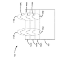
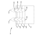
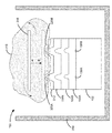
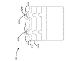
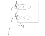
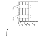
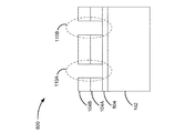
【解決手段】デバイス100の1以上の層104A〜104N上の1以上の持ち上げられた輪郭の高さは、組み合された化学機械研磨/エッチングプロセスを使用して除去される。保護層212が、基板102上で成長したデバイスの上端層に適用され、組み合された化学機械研磨/エッチングプロセスは、保護層の1以上の持ち上げられた輪郭が、平坦化プロセスを介して除去され、保護層の下の層の持ち上げられた輪郭の少なくとも一部分を露出する。材料は、持ち上げられた輪郭の高さを低減するためにエッチング液を使用して除去される。
【選択図】図3
Description
Claims (20)
- デバイスを処理する方法であって、
基板上に材料の少なくとも1つの層をエピタキシャル成長させることであって、材料の前記少なくとも1つの層は欠陥領域を備える、エピタキシャル成長させること、
材料の前記少なくとも1つの層の少なくとも一部分上に保護層を堆積させること、並びに
化学機械平坦化(「CMP」)/エッチングプロセスであって、
前記デバイスを平坦化機械の中に受け入れること、
平坦化パッドを回転させること、
前記欠陥領域の少なくとも一部分からの材料をエッチングするように構成された化合物を含んだスラリを導入すること、
前記欠陥領域のエリアが前記スラリに晒されるまで前記デバイスを平坦化すること、及び
望ましい量の材料が前記欠陥領域から除去されるまで、前記CMP/エッチングプロセスを継続することを含んだ、CMP/エッチングプロセスを実行することを含む、方法。 - 前記平坦化機械から前記デバイスを除去することを更に含む、請求項1に記載の方法。
- 前記CMP/エッチングプロセスの後で、残っている前記保護層の少なくとも一部分を除去することを更に含む、請求項1に記載の方法。
- 前記CMP/エッチングプロセスの後で残っている前記保護層の少なくとも一部分を除去することは、前記保護層をエッチングするために、前記保護層の少なくとも一部分にフッ化水素酸を導入することを含む、請求項3に記載の方法。
- 前記スラリは、前記保護層の硬度を低減させるように構成された化合物を含む、請求項1に記載の方法。
- 前記保護層の前記硬度を低減させるように構成された前記化合物は、酸化剤を含む、請求項5に記載の方法。
- 前記酸化剤は、過酸化物、過酸化水素、ハイドロ過酸化水素、モノ過硫酸塩及びジ過硫酸塩などの過硫酸塩、過炭酸塩、並びにそれらの酸及び塩類を含む、請求項6に記載の方法。
- 前記スラリは、前記欠陥領域内の材料を対象とするように構成されたエッチング液を含む、請求項1に記載の方法。
- 前記エッチング液は、近似的に800:35:4:3の比率の、コロイド状シリカスラリ、H2O、NaOCl、及びクエン酸を含む、請求項8に記載の方法。
- 前記エッチング液は、近似的に2000:100:xの比率の、コロイド状シリカスラリ、H2O2、及びNH4OHを含み、xは3以上である、請求項8に記載の方法。
- コンピュータ可読記憶媒体に記憶された指示命令であって、平坦化機械のプロセッサによって実行されたときに、前記平坦化機械に、
少なくとも1つのエピタキシャル成長した層及び少なくとも1つの保護層を有するウエハを受け入れさせ、前記少なくとも1つのエピタキシャル成長した層は欠陥領域を含み、並びに
化学機械平坦化(「CMP」)/エッチングプロセスであって、
平坦化パッドを回転させ、
前記欠陥領域の少なくとも一部分からの材料をエッチングするように構成された化合物を含んだスラリを導入し、
前記欠陥領域のエリアが前記スラリに晒されるまで前記欠陥領域を平坦化し、及び
望ましい量の材料が前記欠陥領域から除去されるまでCMP/エッチングプロセスを継続することを含んだ、CMP/エッチングプロセスを実行させる、コンピュータ可読記憶媒体に記憶された指示命令を有する、コンピュータ可読記憶媒体。 - 前記平坦化機械から前記ウエハを除去するための指示命令を更に含む、請求項11に記載のコンピュータ可読記憶媒体。
- 前記スラリは、前記少なくとも1つの保護層の硬度を低減させるように構成された化合物を含む、請求項11に記載のコンピュータ可読記憶媒体。
- 前記保護層の前記硬度を低減させるように構成された前記化合物は、酸化剤を含む、請求項11に記載のコンピュータ可読記憶媒体。
- 前記酸化剤は、過酸化物、過酸化水素、ハイドロ過酸化水素、モノ過硫酸塩及びジ過硫酸塩などの過硫酸塩、過炭酸塩、並びにそれらの酸及び塩類を含む、請求項14に記載のコンピュータ可読記憶媒体。
- 前記スラリは、前記欠陥領域内の材料を対象とするように構成されたエッチング液を含む、請求項11に記載のコンピュータ可読記憶媒体。
- 前記エッチング液は、近似的に800:35:4:3の比率の、コロイド状シリカスラリ、H2O、NaOCl、及びクエン酸を含む、請求項16に記載のコンピュータ可読記憶媒体。
- 前記エッチング液は、近似的に2000:100:xの比率の、コロイド状シリカスラリ、H2O2、及びNH4OHを含み、xは3以上である、請求項16に記載のコンピュータ可読記憶媒体。
- 化学機械研磨/エッチングプロセスのためのスラリであって、
保護層の硬度を低減させるように構成された化合物、及び
デバイスの欠陥領域内の材料を対象とするように構成されたエッチング液を含む、スラリ。 - 前記エッチング液は、近似的に800:35:4:3の比率の、コロイド状シリカスラリ、H2O、NaOCl、及びクエン酸、又は近似的に2000:100:xの比率の、コロイド状シリカスラリ、H2O2、及びNH4OHを含み、xは3以上である、請求項19に記載のスラリ。
Applications Claiming Priority (2)
| Application Number | Priority Date | Filing Date | Title |
|---|---|---|---|
| US14/556,337 US9431261B2 (en) | 2014-12-01 | 2014-12-01 | Removal of defects by in-situ etching during chemical-mechanical polishing processing |
| US14/556,337 | 2014-12-01 |
Publications (3)
| Publication Number | Publication Date |
|---|---|
| JP2016129221A true JP2016129221A (ja) | 2016-07-14 |
| JP2016129221A5 JP2016129221A5 (ja) | 2017-05-18 |
| JP6151340B2 JP6151340B2 (ja) | 2017-06-21 |
Family
ID=54542064
Family Applications (1)
| Application Number | Title | Priority Date | Filing Date |
|---|---|---|---|
| JP2015234383A Active JP6151340B2 (ja) | 2014-12-01 | 2015-12-01 | 化学機械研磨加工の間のインシトゥエッチングによる欠陥の除去 |
Country Status (4)
| Country | Link |
|---|---|
| US (1) | US9431261B2 (ja) |
| EP (2) | EP3029717A1 (ja) |
| JP (1) | JP6151340B2 (ja) |
| TW (1) | TWI680508B (ja) |
Families Citing this family (1)
| Publication number | Priority date | Publication date | Assignee | Title |
|---|---|---|---|---|
| CN121013326A (zh) * | 2024-05-22 | 2025-11-25 | 长鑫科技集团股份有限公司 | 半导体结构的制作方法以及半导体结构 |
Citations (3)
| Publication number | Priority date | Publication date | Assignee | Title |
|---|---|---|---|---|
| JP2000315669A (ja) * | 1999-03-18 | 2000-11-14 | Samsung Electronics Co Ltd | 二重研磨阻止層を用いた化学機械的研磨方法 |
| JP2006278981A (ja) * | 2005-03-30 | 2006-10-12 | Fujimi Inc | 単結晶表面用の研磨剤及び研磨方法 |
| US7951719B2 (en) * | 2004-02-25 | 2011-05-31 | Hrl Laboratories, Llc | Self-masking defect removing method |
Family Cites Families (6)
| Publication number | Priority date | Publication date | Assignee | Title |
|---|---|---|---|---|
| JP2000031163A (ja) | 1998-07-13 | 2000-01-28 | Denso Corp | 半導体装置及びその製造方法 |
| US6417109B1 (en) * | 2000-07-26 | 2002-07-09 | Aiwa Co., Ltd. | Chemical-mechanical etch (CME) method for patterned etching of a substrate surface |
| DE102007019565A1 (de) | 2007-04-25 | 2008-09-04 | Siltronic Ag | Verfahren zum einseitigen Polieren von Halbleiterscheiben und Halbleiterscheibe mit einer verspannt-relaxierten Si1-xGex-Schicht |
| RU2605941C2 (ru) | 2011-08-01 | 2016-12-27 | Басф Се | СПОСОБ ИЗГОТОВЛЕНИЯ ПОЛУПРОВОДНИКОВЫХ УСТРОЙСТВ, ВКЛЮЧАЮЩИЙ ХИМИКО-МЕХАНИЧЕСКОЕ ПОЛИРОВАНИЕ ЭЛЕМЕНТАРНОГО ГЕРМАНИЯ И/ИЛИ МАТЕРИАЛА Si1-x Gex В ПРИСУТСТВИИ ХМП (ХИМИКО-МЕХАНИЧЕСКОЙ ПОЛИРОВАЛЬНОЙ) КОМПОЗИЦИИ, ВКЛЮЧАЮЩЕЙ СПЕЦИАЛЬНОЕ ОРГАНИЧЕСКОЕ СОЕДИНЕНИЕ |
| JP6050934B2 (ja) | 2011-11-08 | 2016-12-21 | 株式会社フジミインコーポレーテッド | 研磨用組成物並びにそれを用いた研磨方法及び基板の製造方法 |
| FR2994615A1 (fr) * | 2012-08-14 | 2014-02-21 | Commissariat Energie Atomique | Procede de planarisation d'une couche epitaxiee |
-
2014
- 2014-12-01 US US14/556,337 patent/US9431261B2/en active Active
-
2015
- 2015-11-12 EP EP15194346.1A patent/EP3029717A1/en not_active Ceased
- 2015-11-12 EP EP23168320.2A patent/EP4235751A3/en active Pending
- 2015-12-01 JP JP2015234383A patent/JP6151340B2/ja active Active
- 2015-12-01 TW TW104140023A patent/TWI680508B/zh active
Patent Citations (3)
| Publication number | Priority date | Publication date | Assignee | Title |
|---|---|---|---|---|
| JP2000315669A (ja) * | 1999-03-18 | 2000-11-14 | Samsung Electronics Co Ltd | 二重研磨阻止層を用いた化学機械的研磨方法 |
| US7951719B2 (en) * | 2004-02-25 | 2011-05-31 | Hrl Laboratories, Llc | Self-masking defect removing method |
| JP2006278981A (ja) * | 2005-03-30 | 2006-10-12 | Fujimi Inc | 単結晶表面用の研磨剤及び研磨方法 |
Also Published As
| Publication number | Publication date |
|---|---|
| EP4235751A3 (en) | 2023-11-15 |
| JP6151340B2 (ja) | 2017-06-21 |
| EP4235751A2 (en) | 2023-08-30 |
| US20160155644A1 (en) | 2016-06-02 |
| TW201631652A (zh) | 2016-09-01 |
| US9431261B2 (en) | 2016-08-30 |
| EP3029717A1 (en) | 2016-06-08 |
| TWI680508B (zh) | 2019-12-21 |
Similar Documents
| Publication | Publication Date | Title |
|---|---|---|
| KR102660772B1 (ko) | 자기 제어 및 용해도 제한 반응을 사용하는 습식 원자층 에칭을 위한 공정 시스템 및 플랫폼 | |
| CN104752363B (zh) | 快闪存储器的形成方法 | |
| JP5025508B2 (ja) | ポリシリコン膜の除去方法および記憶媒体 | |
| US20110183522A1 (en) | Method and apparatus for pattern collapse free wet processing of semiconductor devices | |
| TWI666697B (zh) | 基板處理方法、基板處理裝置及記憶媒體 | |
| CN101005025A (zh) | 降低厚度变化的化学机械抛光方法及半导体器件制备方法 | |
| JP2008538857A (ja) | エッチングプロセスのための安定化したフォトレジスト構成 | |
| SG183602A1 (en) | Wiggling control for pseudo-hardmask | |
| JP5015696B2 (ja) | 半導体装置の製造方法及び製造装置 | |
| JP6151340B2 (ja) | 化学機械研磨加工の間のインシトゥエッチングによる欠陥の除去 | |
| CN101197264B (zh) | L型边墙的形成方法 | |
| CN102760653B (zh) | 金属栅极的形成方法 | |
| CN102054665A (zh) | 外延基片处理方法 | |
| US20030124861A1 (en) | Method for manufacturing metal line contact plug semiconductor device | |
| CN101625999A (zh) | Sonos存储器的制作方法 | |
| CN105405754A (zh) | 一种半导体硅片及其平坦化方法、制备方法和半导体器件 | |
| CN115674003A (zh) | 碳化硅晶片的加工方法 | |
| TW506008B (en) | Semiconductor wafer manufacturing process | |
| JP2008021704A (ja) | 半導体装置の製造方法 | |
| CN104681496B (zh) | 半导体结构的形成方法 | |
| JP6864145B1 (ja) | ウェーハの表面形状調整方法 | |
| CN108257885B (zh) | 物理气相沉积中钛或氮化钛颗粒控片的使用方法 | |
| CN111066125A (zh) | 蚀刻并机械研磨堆叠在半导体衬底上的膜层 | |
| KR20050079316A (ko) | 박막 처리 방법 | |
| TW202529195A (zh) | 基板處理方法及基板處理系統 |
Legal Events
| Date | Code | Title | Description |
|---|---|---|---|
| A521 | Request for written amendment filed |
Free format text: JAPANESE INTERMEDIATE CODE: A523 Effective date: 20170321 |
|
| A621 | Written request for application examination |
Free format text: JAPANESE INTERMEDIATE CODE: A621 Effective date: 20170321 |
|
| A871 | Explanation of circumstances concerning accelerated examination |
Free format text: JAPANESE INTERMEDIATE CODE: A871 Effective date: 20170321 |
|
| A975 | Report on accelerated examination |
Free format text: JAPANESE INTERMEDIATE CODE: A971005 Effective date: 20170417 |
|
| TRDD | Decision of grant or rejection written | ||
| A01 | Written decision to grant a patent or to grant a registration (utility model) |
Free format text: JAPANESE INTERMEDIATE CODE: A01 Effective date: 20170425 |
|
| A61 | First payment of annual fees (during grant procedure) |
Free format text: JAPANESE INTERMEDIATE CODE: A61 Effective date: 20170524 |
|
| R150 | Certificate of patent or registration of utility model |
Ref document number: 6151340 Country of ref document: JP Free format text: JAPANESE INTERMEDIATE CODE: R150 |
|
| R250 | Receipt of annual fees |
Free format text: JAPANESE INTERMEDIATE CODE: R250 |
|
| R250 | Receipt of annual fees |
Free format text: JAPANESE INTERMEDIATE CODE: R250 |
|
| R250 | Receipt of annual fees |
Free format text: JAPANESE INTERMEDIATE CODE: R250 |
|
| R250 | Receipt of annual fees |
Free format text: JAPANESE INTERMEDIATE CODE: R250 |
|
| R250 | Receipt of annual fees |
Free format text: JAPANESE INTERMEDIATE CODE: R250 |
|
| R250 | Receipt of annual fees |
Free format text: JAPANESE INTERMEDIATE CODE: R250 |