JP2016127224A - Semiconductor device and semiconductor device manufacturing method - Google Patents
Semiconductor device and semiconductor device manufacturing method Download PDFInfo
- Publication number
- JP2016127224A JP2016127224A JP2015002052A JP2015002052A JP2016127224A JP 2016127224 A JP2016127224 A JP 2016127224A JP 2015002052 A JP2015002052 A JP 2015002052A JP 2015002052 A JP2015002052 A JP 2015002052A JP 2016127224 A JP2016127224 A JP 2016127224A
- Authority
- JP
- Japan
- Prior art keywords
- layer
- hard mask
- barrier metal
- semiconductor device
- metal layer
- Prior art date
- Legal status (The legal status is an assumption and is not a legal conclusion. Google has not performed a legal analysis and makes no representation as to the accuracy of the status listed.)
- Pending
Links
Images


Classifications
-
- H—ELECTRICITY
- H01—ELECTRIC ELEMENTS
- H01L—SEMICONDUCTOR DEVICES NOT COVERED BY CLASS H10
- H01L23/00—Details of semiconductor or other solid state devices
- H01L23/52—Arrangements for conducting electric current within the device in operation from one component to another, i.e. interconnections, e.g. wires, lead frames
- H01L23/522—Arrangements for conducting electric current within the device in operation from one component to another, i.e. interconnections, e.g. wires, lead frames including external interconnections consisting of a multilayer structure of conductive and insulating layers inseparably formed on the semiconductor body
- H01L23/532—Arrangements for conducting electric current within the device in operation from one component to another, i.e. interconnections, e.g. wires, lead frames including external interconnections consisting of a multilayer structure of conductive and insulating layers inseparably formed on the semiconductor body characterised by the materials
- H01L23/53204—Conductive materials
- H01L23/53209—Conductive materials based on metals, e.g. alloys, metal silicides
- H01L23/53214—Conductive materials based on metals, e.g. alloys, metal silicides the principal metal being aluminium
- H01L23/53223—Additional layers associated with aluminium layers, e.g. adhesion, barrier, cladding layers
-
- H—ELECTRICITY
- H01—ELECTRIC ELEMENTS
- H01L—SEMICONDUCTOR DEVICES NOT COVERED BY CLASS H10
- H01L21/00—Processes or apparatus adapted for the manufacture or treatment of semiconductor or solid state devices or of parts thereof
- H01L21/02—Manufacture or treatment of semiconductor devices or of parts thereof
- H01L21/02041—Cleaning
- H01L21/02057—Cleaning during device manufacture
- H01L21/02068—Cleaning during device manufacture during, before or after processing of conductive layers, e.g. polysilicon or amorphous silicon layers
-
- H—ELECTRICITY
- H01—ELECTRIC ELEMENTS
- H01L—SEMICONDUCTOR DEVICES NOT COVERED BY CLASS H10
- H01L21/00—Processes or apparatus adapted for the manufacture or treatment of semiconductor or solid state devices or of parts thereof
- H01L21/02—Manufacture or treatment of semiconductor devices or of parts thereof
- H01L21/027—Making masks on semiconductor bodies for further photolithographic processing not provided for in group H01L21/18 or H01L21/34
- H01L21/0271—Making masks on semiconductor bodies for further photolithographic processing not provided for in group H01L21/18 or H01L21/34 comprising organic layers
- H01L21/0273—Making masks on semiconductor bodies for further photolithographic processing not provided for in group H01L21/18 or H01L21/34 comprising organic layers characterised by the treatment of photoresist layers
- H01L21/0274—Photolithographic processes
- H01L21/0276—Photolithographic processes using an anti-reflective coating
-
- H—ELECTRICITY
- H01—ELECTRIC ELEMENTS
- H01L—SEMICONDUCTOR DEVICES NOT COVERED BY CLASS H10
- H01L21/00—Processes or apparatus adapted for the manufacture or treatment of semiconductor or solid state devices or of parts thereof
- H01L21/02—Manufacture or treatment of semiconductor devices or of parts thereof
- H01L21/027—Making masks on semiconductor bodies for further photolithographic processing not provided for in group H01L21/18 or H01L21/34
- H01L21/033—Making masks on semiconductor bodies for further photolithographic processing not provided for in group H01L21/18 or H01L21/34 comprising inorganic layers
- H01L21/0332—Making masks on semiconductor bodies for further photolithographic processing not provided for in group H01L21/18 or H01L21/34 comprising inorganic layers characterised by their composition, e.g. multilayer masks, materials
-
- H—ELECTRICITY
- H01—ELECTRIC ELEMENTS
- H01L—SEMICONDUCTOR DEVICES NOT COVERED BY CLASS H10
- H01L21/00—Processes or apparatus adapted for the manufacture or treatment of semiconductor or solid state devices or of parts thereof
- H01L21/02—Manufacture or treatment of semiconductor devices or of parts thereof
- H01L21/04—Manufacture or treatment of semiconductor devices or of parts thereof the devices having at least one potential-jump barrier or surface barrier, e.g. PN junction, depletion layer or carrier concentration layer
- H01L21/18—Manufacture or treatment of semiconductor devices or of parts thereof the devices having at least one potential-jump barrier or surface barrier, e.g. PN junction, depletion layer or carrier concentration layer the devices having semiconductor bodies comprising elements of Group IV of the Periodic System or AIIIBV compounds with or without impurities, e.g. doping materials
- H01L21/30—Treatment of semiconductor bodies using processes or apparatus not provided for in groups H01L21/20 - H01L21/26
- H01L21/31—Treatment of semiconductor bodies using processes or apparatus not provided for in groups H01L21/20 - H01L21/26 to form insulating layers thereon, e.g. for masking or by using photolithographic techniques; After treatment of these layers; Selection of materials for these layers
- H01L21/3105—After-treatment
- H01L21/311—Etching the insulating layers by chemical or physical means
- H01L21/31105—Etching inorganic layers
- H01L21/31111—Etching inorganic layers by chemical means
- H01L21/31116—Etching inorganic layers by chemical means by dry-etching
-
- H—ELECTRICITY
- H01—ELECTRIC ELEMENTS
- H01L—SEMICONDUCTOR DEVICES NOT COVERED BY CLASS H10
- H01L21/00—Processes or apparatus adapted for the manufacture or treatment of semiconductor or solid state devices or of parts thereof
- H01L21/02—Manufacture or treatment of semiconductor devices or of parts thereof
- H01L21/04—Manufacture or treatment of semiconductor devices or of parts thereof the devices having at least one potential-jump barrier or surface barrier, e.g. PN junction, depletion layer or carrier concentration layer
- H01L21/18—Manufacture or treatment of semiconductor devices or of parts thereof the devices having at least one potential-jump barrier or surface barrier, e.g. PN junction, depletion layer or carrier concentration layer the devices having semiconductor bodies comprising elements of Group IV of the Periodic System or AIIIBV compounds with or without impurities, e.g. doping materials
- H01L21/30—Treatment of semiconductor bodies using processes or apparatus not provided for in groups H01L21/20 - H01L21/26
- H01L21/31—Treatment of semiconductor bodies using processes or apparatus not provided for in groups H01L21/20 - H01L21/26 to form insulating layers thereon, e.g. for masking or by using photolithographic techniques; After treatment of these layers; Selection of materials for these layers
- H01L21/3105—After-treatment
- H01L21/311—Etching the insulating layers by chemical or physical means
- H01L21/31127—Etching organic layers
- H01L21/31133—Etching organic layers by chemical means
- H01L21/31138—Etching organic layers by chemical means by dry-etching
-
- H—ELECTRICITY
- H01—ELECTRIC ELEMENTS
- H01L—SEMICONDUCTOR DEVICES NOT COVERED BY CLASS H10
- H01L21/00—Processes or apparatus adapted for the manufacture or treatment of semiconductor or solid state devices or of parts thereof
- H01L21/02—Manufacture or treatment of semiconductor devices or of parts thereof
- H01L21/04—Manufacture or treatment of semiconductor devices or of parts thereof the devices having at least one potential-jump barrier or surface barrier, e.g. PN junction, depletion layer or carrier concentration layer
- H01L21/18—Manufacture or treatment of semiconductor devices or of parts thereof the devices having at least one potential-jump barrier or surface barrier, e.g. PN junction, depletion layer or carrier concentration layer the devices having semiconductor bodies comprising elements of Group IV of the Periodic System or AIIIBV compounds with or without impurities, e.g. doping materials
- H01L21/30—Treatment of semiconductor bodies using processes or apparatus not provided for in groups H01L21/20 - H01L21/26
- H01L21/31—Treatment of semiconductor bodies using processes or apparatus not provided for in groups H01L21/20 - H01L21/26 to form insulating layers thereon, e.g. for masking or by using photolithographic techniques; After treatment of these layers; Selection of materials for these layers
- H01L21/3205—Deposition of non-insulating-, e.g. conductive- or resistive-, layers on insulating layers; After-treatment of these layers
- H01L21/321—After treatment
- H01L21/3213—Physical or chemical etching of the layers, e.g. to produce a patterned layer from a pre-deposited extensive layer
- H01L21/32133—Physical or chemical etching of the layers, e.g. to produce a patterned layer from a pre-deposited extensive layer by chemical means only
- H01L21/32134—Physical or chemical etching of the layers, e.g. to produce a patterned layer from a pre-deposited extensive layer by chemical means only by liquid etching only
-
- H—ELECTRICITY
- H01—ELECTRIC ELEMENTS
- H01L—SEMICONDUCTOR DEVICES NOT COVERED BY CLASS H10
- H01L21/00—Processes or apparatus adapted for the manufacture or treatment of semiconductor or solid state devices or of parts thereof
- H01L21/02—Manufacture or treatment of semiconductor devices or of parts thereof
- H01L21/04—Manufacture or treatment of semiconductor devices or of parts thereof the devices having at least one potential-jump barrier or surface barrier, e.g. PN junction, depletion layer or carrier concentration layer
- H01L21/18—Manufacture or treatment of semiconductor devices or of parts thereof the devices having at least one potential-jump barrier or surface barrier, e.g. PN junction, depletion layer or carrier concentration layer the devices having semiconductor bodies comprising elements of Group IV of the Periodic System or AIIIBV compounds with or without impurities, e.g. doping materials
- H01L21/30—Treatment of semiconductor bodies using processes or apparatus not provided for in groups H01L21/20 - H01L21/26
- H01L21/31—Treatment of semiconductor bodies using processes or apparatus not provided for in groups H01L21/20 - H01L21/26 to form insulating layers thereon, e.g. for masking or by using photolithographic techniques; After treatment of these layers; Selection of materials for these layers
- H01L21/3205—Deposition of non-insulating-, e.g. conductive- or resistive-, layers on insulating layers; After-treatment of these layers
- H01L21/321—After treatment
- H01L21/3213—Physical or chemical etching of the layers, e.g. to produce a patterned layer from a pre-deposited extensive layer
- H01L21/32133—Physical or chemical etching of the layers, e.g. to produce a patterned layer from a pre-deposited extensive layer by chemical means only
- H01L21/32135—Physical or chemical etching of the layers, e.g. to produce a patterned layer from a pre-deposited extensive layer by chemical means only by vapour etching only
- H01L21/32138—Physical or chemical etching of the layers, e.g. to produce a patterned layer from a pre-deposited extensive layer by chemical means only by vapour etching only pre- or post-treatments, e.g. anti-corrosion processes
-
- H—ELECTRICITY
- H01—ELECTRIC ELEMENTS
- H01L—SEMICONDUCTOR DEVICES NOT COVERED BY CLASS H10
- H01L21/00—Processes or apparatus adapted for the manufacture or treatment of semiconductor or solid state devices or of parts thereof
- H01L21/02—Manufacture or treatment of semiconductor devices or of parts thereof
- H01L21/04—Manufacture or treatment of semiconductor devices or of parts thereof the devices having at least one potential-jump barrier or surface barrier, e.g. PN junction, depletion layer or carrier concentration layer
- H01L21/18—Manufacture or treatment of semiconductor devices or of parts thereof the devices having at least one potential-jump barrier or surface barrier, e.g. PN junction, depletion layer or carrier concentration layer the devices having semiconductor bodies comprising elements of Group IV of the Periodic System or AIIIBV compounds with or without impurities, e.g. doping materials
- H01L21/30—Treatment of semiconductor bodies using processes or apparatus not provided for in groups H01L21/20 - H01L21/26
- H01L21/31—Treatment of semiconductor bodies using processes or apparatus not provided for in groups H01L21/20 - H01L21/26 to form insulating layers thereon, e.g. for masking or by using photolithographic techniques; After treatment of these layers; Selection of materials for these layers
- H01L21/3205—Deposition of non-insulating-, e.g. conductive- or resistive-, layers on insulating layers; After-treatment of these layers
- H01L21/321—After treatment
- H01L21/3213—Physical or chemical etching of the layers, e.g. to produce a patterned layer from a pre-deposited extensive layer
- H01L21/32139—Physical or chemical etching of the layers, e.g. to produce a patterned layer from a pre-deposited extensive layer using masks
-
- H—ELECTRICITY
- H01—ELECTRIC ELEMENTS
- H01L—SEMICONDUCTOR DEVICES NOT COVERED BY CLASS H10
- H01L21/00—Processes or apparatus adapted for the manufacture or treatment of semiconductor or solid state devices or of parts thereof
- H01L21/70—Manufacture or treatment of devices consisting of a plurality of solid state components formed in or on a common substrate or of parts thereof; Manufacture of integrated circuit devices or of parts thereof
- H01L21/71—Manufacture of specific parts of devices defined in group H01L21/70
- H01L21/768—Applying interconnections to be used for carrying current between separate components within a device comprising conductors and dielectrics
- H01L21/76801—Applying interconnections to be used for carrying current between separate components within a device comprising conductors and dielectrics characterised by the formation and the after-treatment of the dielectrics, e.g. smoothing
- H01L21/76829—Applying interconnections to be used for carrying current between separate components within a device comprising conductors and dielectrics characterised by the formation and the after-treatment of the dielectrics, e.g. smoothing characterised by the formation of thin functional dielectric layers, e.g. dielectric etch-stop, barrier, capping or liner layers
- H01L21/76834—Applying interconnections to be used for carrying current between separate components within a device comprising conductors and dielectrics characterised by the formation and the after-treatment of the dielectrics, e.g. smoothing characterised by the formation of thin functional dielectric layers, e.g. dielectric etch-stop, barrier, capping or liner layers formation of thin insulating films on the sidewalls or on top of conductors
-
- H—ELECTRICITY
- H01—ELECTRIC ELEMENTS
- H01L—SEMICONDUCTOR DEVICES NOT COVERED BY CLASS H10
- H01L21/00—Processes or apparatus adapted for the manufacture or treatment of semiconductor or solid state devices or of parts thereof
- H01L21/70—Manufacture or treatment of devices consisting of a plurality of solid state components formed in or on a common substrate or of parts thereof; Manufacture of integrated circuit devices or of parts thereof
- H01L21/71—Manufacture of specific parts of devices defined in group H01L21/70
- H01L21/768—Applying interconnections to be used for carrying current between separate components within a device comprising conductors and dielectrics
- H01L21/76838—Applying interconnections to be used for carrying current between separate components within a device comprising conductors and dielectrics characterised by the formation and the after-treatment of the conductors
- H01L21/76841—Barrier, adhesion or liner layers
- H01L21/76853—Barrier, adhesion or liner layers characterized by particular after-treatment steps
- H01L21/76865—Selective removal of parts of the layer
-
- H—ELECTRICITY
- H01—ELECTRIC ELEMENTS
- H01L—SEMICONDUCTOR DEVICES NOT COVERED BY CLASS H10
- H01L21/00—Processes or apparatus adapted for the manufacture or treatment of semiconductor or solid state devices or of parts thereof
- H01L21/70—Manufacture or treatment of devices consisting of a plurality of solid state components formed in or on a common substrate or of parts thereof; Manufacture of integrated circuit devices or of parts thereof
- H01L21/71—Manufacture of specific parts of devices defined in group H01L21/70
- H01L21/768—Applying interconnections to be used for carrying current between separate components within a device comprising conductors and dielectrics
- H01L21/76838—Applying interconnections to be used for carrying current between separate components within a device comprising conductors and dielectrics characterised by the formation and the after-treatment of the conductors
- H01L21/76885—By forming conductive members before deposition of protective insulating material, e.g. pillars, studs
-
- H—ELECTRICITY
- H01—ELECTRIC ELEMENTS
- H01L—SEMICONDUCTOR DEVICES NOT COVERED BY CLASS H10
- H01L21/00—Processes or apparatus adapted for the manufacture or treatment of semiconductor or solid state devices or of parts thereof
- H01L21/70—Manufacture or treatment of devices consisting of a plurality of solid state components formed in or on a common substrate or of parts thereof; Manufacture of integrated circuit devices or of parts thereof
- H01L21/71—Manufacture of specific parts of devices defined in group H01L21/70
- H01L21/768—Applying interconnections to be used for carrying current between separate components within a device comprising conductors and dielectrics
- H01L21/76838—Applying interconnections to be used for carrying current between separate components within a device comprising conductors and dielectrics characterised by the formation and the after-treatment of the conductors
- H01L21/76886—Modifying permanently or temporarily the pattern or the conductivity of conductive members, e.g. formation of alloys, reduction of contact resistances
- H01L21/76892—Modifying permanently or temporarily the pattern or the conductivity of conductive members, e.g. formation of alloys, reduction of contact resistances modifying the pattern
-
- H—ELECTRICITY
- H01—ELECTRIC ELEMENTS
- H01L—SEMICONDUCTOR DEVICES NOT COVERED BY CLASS H10
- H01L23/00—Details of semiconductor or other solid state devices
- H01L23/52—Arrangements for conducting electric current within the device in operation from one component to another, i.e. interconnections, e.g. wires, lead frames
- H01L23/522—Arrangements for conducting electric current within the device in operation from one component to another, i.e. interconnections, e.g. wires, lead frames including external interconnections consisting of a multilayer structure of conductive and insulating layers inseparably formed on the semiconductor body
- H01L23/528—Geometry or layout of the interconnection structure
-
- H—ELECTRICITY
- H01—ELECTRIC ELEMENTS
- H01L—SEMICONDUCTOR DEVICES NOT COVERED BY CLASS H10
- H01L21/00—Processes or apparatus adapted for the manufacture or treatment of semiconductor or solid state devices or of parts thereof
- H01L21/02—Manufacture or treatment of semiconductor devices or of parts thereof
- H01L21/04—Manufacture or treatment of semiconductor devices or of parts thereof the devices having at least one potential-jump barrier or surface barrier, e.g. PN junction, depletion layer or carrier concentration layer
- H01L21/18—Manufacture or treatment of semiconductor devices or of parts thereof the devices having at least one potential-jump barrier or surface barrier, e.g. PN junction, depletion layer or carrier concentration layer the devices having semiconductor bodies comprising elements of Group IV of the Periodic System or AIIIBV compounds with or without impurities, e.g. doping materials
- H01L21/30—Treatment of semiconductor bodies using processes or apparatus not provided for in groups H01L21/20 - H01L21/26
- H01L21/31—Treatment of semiconductor bodies using processes or apparatus not provided for in groups H01L21/20 - H01L21/26 to form insulating layers thereon, e.g. for masking or by using photolithographic techniques; After treatment of these layers; Selection of materials for these layers
- H01L21/3205—Deposition of non-insulating-, e.g. conductive- or resistive-, layers on insulating layers; After-treatment of these layers
- H01L21/321—After treatment
- H01L21/3213—Physical or chemical etching of the layers, e.g. to produce a patterned layer from a pre-deposited extensive layer
- H01L21/32133—Physical or chemical etching of the layers, e.g. to produce a patterned layer from a pre-deposited extensive layer by chemical means only
- H01L21/32135—Physical or chemical etching of the layers, e.g. to produce a patterned layer from a pre-deposited extensive layer by chemical means only by vapour etching only
- H01L21/32136—Physical or chemical etching of the layers, e.g. to produce a patterned layer from a pre-deposited extensive layer by chemical means only by vapour etching only using plasmas
-
- H—ELECTRICITY
- H01—ELECTRIC ELEMENTS
- H01L—SEMICONDUCTOR DEVICES NOT COVERED BY CLASS H10
- H01L2924/00—Indexing scheme for arrangements or methods for connecting or disconnecting semiconductor or solid-state bodies as covered by H01L24/00
- H01L2924/0001—Technical content checked by a classifier
- H01L2924/0002—Not covered by any one of groups H01L24/00, H01L24/00 and H01L2224/00
Abstract
Description
本発明は、積層構造の金属配線を有する半導体装置及び半導体装置の製造方法に関するものである。 The present invention relates to a semiconductor device having a metal wiring having a laminated structure and a method for manufacturing the semiconductor device.
従来、LSI等に用いる半導体装置では、アルミニウムを用いた積層構造の金属配線を微細加工することで、金属配線におけるライン&スペースの縮小が行われてきた。微細加工の方法としては、ハードマスクをマスクとして金属配線となる積層膜のドライエッチングを行うハードマスクプロセスが知られている。 Conventionally, in a semiconductor device used for an LSI or the like, line and space in a metal wiring has been reduced by finely processing a metal wiring having a laminated structure using aluminum. As a microfabrication method, a hard mask process is known in which dry etching is performed on a laminated film serving as metal wiring using a hard mask as a mask.
しかしながら、ハードマスクプロセスにおける不具合として、ハードマスクを形成する際に生じるパターン欠陥が問題となっている。このパターン欠陥は、上記ハードマスクの形成時に、本来ハードマスクが形成されない領域に堆積物や反応生成物が形成されることにより生じるものである。これら堆積物や反応生成物は、被エッチング材料である積層膜のエッチングを妨げるため、形成される金属配線における配線ショートの原因となる。その原因となる堆積物や反応生成物は、ハードマスクのエッチングやその後の洗浄工程にて生じるものと考えられている。 However, as a defect in the hard mask process, a pattern defect generated when forming a hard mask is a problem. This pattern defect is caused when a deposit or a reaction product is formed in a region where the hard mask is not originally formed when the hard mask is formed. Since these deposits and reaction products hinder the etching of the laminated film that is the material to be etched, it causes a wiring short in the formed metal wiring. It is believed that the deposits and reaction products that cause this are generated in the etching of the hard mask and the subsequent cleaning process.
これに対して、特許文献1には、ハードマスクを形成する工程の後に、最上部が窒化チタン層により構成される下地層及びハードマスクの露出部分を、フッ素を含まない洗浄液を用いて洗浄する工程を有する電子デバイスの製造方法が記載されている。特許文献1によれば、フッ素を含まない洗浄液を用いて洗浄することにより、窒化チタン層中のチタンとフッ素との反応生成物からなる堆積物の発生を抑制することが可能であるとされている。 On the other hand, in Patent Document 1, after the step of forming the hard mask, the underlying layer composed of a titanium nitride layer at the top and the exposed portion of the hard mask are cleaned using a cleaning liquid that does not contain fluorine. A method of manufacturing an electronic device having steps is described. According to Patent Document 1, it is said that it is possible to suppress the generation of deposits composed of reaction products of titanium and fluorine in the titanium nitride layer by cleaning using a cleaning liquid that does not contain fluorine. Yes.
しかしながら、上記特許文献1によれば、チタンとフッ素との反応生成物を低減させることができるとしても、一方で、特許文献1では、その他の反応生成物について言及されていない。具体的には、特許文献1では、ハードマスクのドライエッチングに酸素を含む反応ガスを用いており、また、窒化チタン層が露出してからのオーバーエッチング量についても言及がない。したがって、チタンと酸素との反応生成物が生じる場合があると考えられる。チタンと酸素との反応生成物が生じた場合も、金属配線となる積層膜のエッチングが反応生成物により妨げられ、これにより、配線ショートが発生するおそれがある。 However, according to Patent Document 1, although the reaction product of titanium and fluorine can be reduced, Patent Document 1 does not mention other reaction products. Specifically, in Patent Document 1, a reactive gas containing oxygen is used for dry etching of the hard mask, and there is no mention of the amount of overetching after the titanium nitride layer is exposed. Therefore, it is considered that a reaction product of titanium and oxygen may be generated. Even when a reaction product of titanium and oxygen is generated, etching of the laminated film to be a metal wiring is hindered by the reaction product, which may cause a wiring short circuit.
本発明の目的は、金属配線の微細加工を実現するとともに、配線ショートの発生を抑制することができる半導体装置及び半導体装置の製造方法を提供することにある。 An object of the present invention is to provide a semiconductor device and a method of manufacturing the semiconductor device that can realize fine processing of metal wiring and can suppress the occurrence of wiring short-circuit.
上記課題に鑑み、本発明の一観点による半導体装置の製造方法は、アルミニウムを主成分とする導電層と、前記導電層上に形成されたバリアメタル層とを有する積層膜を形成する工程と、前記バリアメタル層上にハードマスク層を形成する工程と、前記ハードマスク層上にレジストをパターニングする工程と、パターニングされた前記レジストをマスクとして前記ハードマスク層をドライエッチングし、前記ハードマスク層をパターニングする工程と、前記ハードマスク層をパターニングする工程の後、前記バリアメタル層の表面を洗浄液で洗浄する工程と、前記バリアメタル層の表面を洗浄する工程の後、パターニングされた前記ハードマスク層をマスクとして前記積層膜をドライエッチングする工程とを有し、前記ハードマスク層をパターニングする工程では、前記バリアメタル層がプロセスガスに曝された状態においては、前記プロセスガスの総流量に対する酸化ガスの流量の比率を1%未満としてドライエッチングすることを特徴とする。 In view of the above problems, a method of manufacturing a semiconductor device according to an aspect of the present invention includes a step of forming a laminated film including a conductive layer mainly composed of aluminum and a barrier metal layer formed on the conductive layer. Forming a hard mask layer on the barrier metal layer; patterning a resist on the hard mask layer; dry etching the hard mask layer using the patterned resist as a mask; After the patterning step, the step of patterning the hard mask layer, the step of cleaning the surface of the barrier metal layer with a cleaning liquid, and the step of cleaning the surface of the barrier metal layer, the patterned hard mask layer And a step of dry etching the laminated film using a mask as a mask. The training to process, the barrier metal layer in a state of being exposed to the process gas, characterized by dry-etching the ratio of the flow rate of the oxidizing gas to the total flow rate of the process gas as less than 1%.
また、本発明の他の観点による半導体装置は、アルミニウムを主成分とする導電層と、前記導電層上に形成されたバリアメタル層とを有する金属配線と、前記バリアメタル層上に形成されたハードマスク層とを有し、前記ハードマスク層の下面の幅が、前記バリアメタル層の上面の幅よりも広く、前記バリアメタル層の下面の幅が、前記バリアメタル層の上面の幅よりも広いことを特徴とする。 In addition, a semiconductor device according to another aspect of the present invention is formed on a metal wiring having a conductive layer mainly composed of aluminum and a barrier metal layer formed on the conductive layer, and the barrier metal layer. A hard mask layer, the lower surface of the hard mask layer is wider than the upper surface of the barrier metal layer, and the lower surface of the barrier metal layer is wider than the upper surface of the barrier metal layer. It is wide.
本発明によれば、金属配線の微細加工を実現するとともに、配線ショートの発生を抑制することができる。 According to the present invention, it is possible to realize fine processing of metal wiring and to suppress the occurrence of wiring short circuit.
[第1の実施形態]
本発明の第1の実施形態に係る半導体装置及び半導体装置の製造方法について図面を参照して説明する。第1乃至第5の実施形態の各実施形態で説明する半導体装置は例えば固体撮像装置であるが、本発明の半導体装置は、固体撮像装置に限定されるものではなく、金属配線を有する半導体装置であればよい。なお、本発明の半導体装置の一例である固体撮像装置の画素配列領域及び周辺領域を含む全体構成については後述する。
[First Embodiment]
A semiconductor device and a semiconductor device manufacturing method according to a first embodiment of the present invention will be described with reference to the drawings. The semiconductor device described in each of the first to fifth embodiments is, for example, a solid-state imaging device. However, the semiconductor device of the present invention is not limited to the solid-state imaging device, and a semiconductor device having a metal wiring. If it is. Note that an overall configuration including a pixel array region and a peripheral region of a solid-state imaging device which is an example of the semiconductor device of the present invention will be described later.
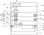
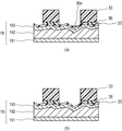
まず、本実施形態に係る半導体装置の断面構成について図1及び図2を用いて説明する。図1は、本実施形態に係る半導体装置を示す概略断面図である。図2は、本実施形態に係る半導体装置における金属配線を示す概略断面図である。 First, a cross-sectional configuration of the semiconductor device according to the present embodiment will be described with reference to FIGS. FIG. 1 is a schematic cross-sectional view showing the semiconductor device according to the present embodiment. FIG. 2 is a schematic cross-sectional view showing metal wiring in the semiconductor device according to the present embodiment.
図1に示すように、半導体基板である例えばシリコン基板11には、素子領域を画定する、STIやLOCOSなどの絶縁体からなる素子分離部12が形成されている。素子領域のシリコン基板11内には、ウェル拡散層13が形成されている。
As shown in FIG. 1, an
シリコン基板11のウェル拡散層13が形成された領域上には、ゲート絶縁膜を介してゲート電極14が形成されている。ゲート電極14は、例えばポリシリコンよりなるポリシリコンゲートである。また、ゲート電極14の両側のウェル拡散層13内には、フォトダイオードを構成するフォトダイオード拡散層15、及びソース/ドレイン拡散層16がそれぞれ形成されている。
On the region of the
シリコン基板11上には、層間絶縁層17が形成されている。層間絶縁層17には、ソース/ドレイン拡散層16に達するコンタクトホールが形成されており、このコンタクトホールには、ソース/ドレイン拡散層16に電気的に接続されたコンタクトプラグ18が埋め込まれている。
On the
層間絶縁層17上には、第1の金属配線19が形成されている。第1の金属配線19は、積層構造を有し、例えば、バリアメタル層191と、導電層192と、バリアメタル層193とが順次積層されてなる積層膜により構成されている。バリアメタル膜191は、例えば、チタン層と窒化チタン層とが順次積層されてなる積層膜により構成されている。また、導電層192はアルミニウムを主成分としており、例えば、アルミニウム層又はAlCu合金層等のアルミニウム合金層により構成されている。また、導電層上のバリアメタル層193は、例えば、チタン層と窒化チタン層とが順次積層されてなる積層膜により構成されている。なお、バリアメタル層191、193は、チタン層を含まず、窒化チタン層により構成されていてもよい。バリアメタル層191、193は、アルミニウム層又はアルミニウム合金層により構成される導電層192の材料が周囲の部材、例えばコンタクトプラグ18やビアプラグ22に拡散するのを抑制するためのものである。
A
第1の金属配線19は、コンタクトプラグ18を介して、ソース/ドレイン拡散層16に電気的に接続されている。第1の金属配線19のバリアメタル層193上には、ハードマスクとして機能する絶縁層であるハードマスク層20が形成されている。なお、バリアメタル層上のハードマスク層20は、後述するように、第1の金属配線19をパターニングするためのドライエッチングにおいてハードマスクとして用いられたものである。
The
第1の金属配線19が形成された層間絶縁層17上には、層間絶縁層21が形成されている。層間絶縁層21及びハードマスク層20には、第1の金属配線19に達するスルーホールが形成されており、このスルーホールには、第1の金属配線19に電気的に接続されたビアプラグ22が埋め込まれている。
An
層間絶縁層21上には、第2の金属配線23が形成されている。第2の金属配線23は、積層構造を有し、例えば、バリアメタル層231と、導電層232と、バリアメタル層233とが順次積層されてなる積層膜により構成されている。バリアメタル層231は、例えば、チタン層と窒化チタン層とが順次積層されてなる積層膜により構成されている。また、導電層232はアルミニウムを主成分としており、例えば、アルミニウム層又はAlCu合金層等のアルミニウム合金層により構成されている。また、導電層上のバリアメタル層233は、例えば、チタン層と窒化チタン層とが順次積層されてなる積層膜により構成されている。なお、バリアメタル層231、233は、チタン層を含まず、窒化チタン層により構成されていてもよい。バリアメタル層231、233は、アルミニウム層又はアルミニウム合金層により構成される導電層232の材料が周囲の部材、例えばビアプラグ22やビアプラグ26に拡散するのを抑制するためのものである。
A
第2の金属配線23は、ビアプラグ22を介して、第1の金属配線19に電気的に接続されている。第2の金属配線23のバリアメタル層233上には、ハードマスクとして機能する絶縁層であるハードマスク層24が形成されている。なお、バリアメタル層上のハードマスク層24は、後述するように、第2の金属配線23をパターニングするためのドライエッチングにおいてハードマスクとして用いられたものである。
The
第2の金属配線23が形成された層間絶縁層21上には、層間絶縁層25が形成されている。層間絶縁層25及びハードマスク層24には、第2の金属配線23に達するスルーホールが形成されており、このスルーホールには、第2の金属配線23に電気的に接続されたビアプラグ26が埋め込まれている。
An interlayer insulating
層間絶縁層25上には、第3の金属配線27が形成されている。第3の金属配線27は、アルミニウム層又はAlCu合金層等のアルミニウム合金層により構成されている。なお、第3の金属配線27は、第1及び第2の金属配線19、23と同様に、バリアメタル層を有する積層膜により構成されていてもよい。第3の金属配線27は、ビアプラグ26を介して、第2の金属配線23に電気的に接続されている。
A
第3の金属配線27が形成された層間絶縁層25上には、層間絶縁層28が形成されている。層間絶縁層28には、第3の金属配線27に達するスルーホールが形成されており、このスルーホールには、第3の金属配線27に電気的に接続されたビアプラグ29が埋め込まれている。
On the
層間絶縁層28上には、ボンディングパッドを含む第4の金属配線30が形成されている。第4の金属配線30は、アルミニウム層又はAlCu合金層等のアルミニウム合金層により構成されている。なお、第4の金属配線30は、第1及び第2の金属配線19、23と同様に、バリアメタル層を有する積層膜により構成されていてもよい。第4の金属配線30は、ビアプラグ29を介して、第3の金属配線27に電気的に接続されている。
On the
第4の金属配線30が形成された層間絶縁層28上には、保護絶縁膜31が形成されている。保護絶縁膜31には、第4の金属配線30のボンディングパッドに達する開口部32が形成されている。保護絶縁膜31は窒化シリコンなどからなる。
A protective insulating
なお、上記の層間絶縁層17、ハードマスク層20、24、層間絶縁層21、25、28としては、例えば、BPSG(Boro-Phospho Silicate Glass)層、酸化シリコン層等の絶縁層を用いることができる。また、保護絶縁膜31としては、例えば、窒化シリコン層や酸窒化シリコン層、酸化シリコン層等の単層または複層の絶縁膜を用いることができる。
In addition, as said
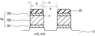
続いて、本実施形態に係る半導体装置における金属配線の具体的構造について図2を用いて説明する。図2は、本実施形態に係る半導体装置における金属配線を示す概略断面図であり、具体的には、第1の金属配線19の断面構造を示している。
Next, a specific structure of the metal wiring in the semiconductor device according to the present embodiment will be described with reference to FIG. FIG. 2 is a schematic cross-sectional view showing the metal wiring in the semiconductor device according to the present embodiment. Specifically, the cross-sectional structure of the
図2に示すように、層間絶縁層17上に形成された第1の金属配線19は、バリアメタル層191と、バリアメタル層191上に形成された導電層192と、導電層192上に形成されたバリアメタル層193とを有している。また、第1の金属配線19のバリアメタル層193上には、ハードマスク層20が形成されている。
As shown in FIG. 2, the
第1の金属配線19の上側のバリアメタル層193は、少なくともその上部において上面側から下面側に向かって徐々に幅広となるテーパ形状を有している。また、バリアメタル層193上のハードマスク層20も、少なくともその上部において上面側から下面側に向かって徐々に幅広となるテーパ形状を有している。
The
ここで、ハードマスク層20の下面の幅をa(nm)、バリアメタル層193の上面の幅をb(nm)、バリアメタル層193の下面の幅をc(nm)とする。ハードマスク層20及びバリアメタル層193は、これらの幅a、b、及びcが次の大小関係を満足する構造的な特徴を有している。
a>b、かつc>b
Here, the width of the lower surface of the
a> b and c> b
すなわち、ハードマスク層20の下面の幅aが、バリアメタル層193の上面の幅bよりも広くなっている。さらに、バリアメタル層193の下面の幅cが、バリアメタル層193の上面の幅bよりも広くなっている。
That is, the width a of the lower surface of the
上記図2に示す構造的な特徴は、ハードマスク層20をパターニングするためのドライエッチング後のウェットエッチングの際に生じたものである。すなわち、この構造的な特徴は、ハードマスク層20が除去されて露出したバリアメタル層193の上部の一部がウェットエッチングされて除去されるとともに、バリアメタル層193に対してサイドエッチングが入ることによるものである。後述するように、バリアメタル層193の上部の一部を除去することで、反応生成物やエッチング残渣を含む異物を効率よく除去することができ、配線工程における歩留りを改善することができる。
The structural features shown in FIG. 2 are caused by wet etching after dry etching for patterning the
なお、図2には第1の金属配線19の断面構造を示したが、第2の金属配線23も、ハードマスク層24及びバリアメタル層233に関し、第1の金属配線19と同様の構造的な特徴を有している。
2 shows the cross-sectional structure of the
次に、本実施形態に係る半導体装置の製造方法について図3乃至図6を用いて説明する。図3乃至図5は、本実施形態に係る半導体装置の製造方法を示す工程断面図である。図6は、本実施形態に係る半導体装置の製造方法における第1の金属配線の形成工程を示すフローチャートである。 Next, a method for manufacturing the semiconductor device according to the present embodiment will be described with reference to FIGS. 3 to 5 are process cross-sectional views illustrating the method for manufacturing the semiconductor device according to the present embodiment. FIG. 6 is a flowchart showing a first metal wiring forming step in the method of manufacturing a semiconductor device according to this embodiment.
なお、以下の説明においては、簡略化のために金属配線の製造方法の要部を中心に説明するが、記載のない部分については通常の固体撮像装置の製造方法により形成されるものとする。 In the following description, for the sake of simplification, the description will focus on the main part of the metal wiring manufacturing method. However, parts not described are formed by a normal solid-state imaging device manufacturing method.
まず、図3(a)に示すように、シリコン基板11に、素子分離部12を形成し、素子分離部12により素子領域を画定する。また、素子領域のシリコン基板11内に、ウェル拡散層13を形成する。また、ウェル拡散層13が形成されたシリコン基板11上に、ゲート絶縁層を介してゲート電極14を形成する。また、ゲート電極14の両側のウェル拡散層13内に、フォトダイオード拡散層15、ソース/ドレイン拡散層16を形成する。次いで、シリコン基板11上に、層間絶縁層17を形成する。層間絶縁層17には、ソース/ドレイン拡散層16に達するコンタクトホールを開口した後、このコンタクトホールに埋め込まれたコンタクトプラグ18を形成する。なお、これら図3(a)に示す各部の形成には、一般的な半導体装置の製造プロセスを用いることができる。
First, as shown in FIG. 3A, the
次に、次工程の第1の金属配線19の形成工程について詳細に説明をする。説明に際しては、図6に示すフローチャートをさらに参照する。
Next, the process for forming the
まず、層間絶縁層17上に、例えばスパッタリング法により、例えば厚さ約10nmのチタン層と、例えば厚さ約20nmの窒化チタン層とを順次成膜し、これらチタン層と窒化チタン層とが順次積層されてなるバリアメタル層191を形成する。
First, a titanium layer having a thickness of, for example, about 10 nm and a titanium nitride layer having a thickness of, for example, about 20 nm are sequentially formed on the
次いで、バリアメタル層191上に、例えばスパッタリング法により、例えばCuを約0.5wt%含んだAlCuよりなる厚さ約230nmのアルミニウム合金層を約300℃の成膜温度で成膜し、このアルミニウム合金層よりなる導電層192を形成する。
Next, an aluminum alloy layer having a thickness of about 230 nm made of AlCu containing, for example, about 0.5 wt% of Cu is formed on the
次いで、導電層192上に、例えばスパッタリング法により、例えば厚さ約3nmのチタン層と、例えば厚さ約30nmの窒化チタン層とを順次成膜し、これらチタン層と窒化チタン層とが順次積層されてなるバリアメタル層193を形成する。
Next, a titanium layer having a thickness of, for example, about 3 nm and a titanium nitride layer having a thickness of, for example, about 30 nm are sequentially formed on the
こうして、層間絶縁層17上に、バリアメタル層191と導電層192とバリアメタル層193とを有し、第1の金属配線19に加工される積層膜が形成される(図6:工程S11)。
Thus, a laminated film having the
次に、バリアメタル層193上に、例えばプラズマCVD(Chemical Vapor Deposition)法により、例えば厚さ約100nm〜200nmのシリコン酸化層よりなるハードマスク層20を形成する(図6:工程S12)。ハードマスク層20を構成するシリコン酸化層は、例えば、約300〜400℃の成膜温度で、TEOS(Tetraethyl orthosilicate、Si(OC2H5)4)とO2とをプラズマ状態で反応させることにより形成することができる。
Next, a
次に、図3(b)に示すように、ハードマスク層20上に、フォトリソグラフィにより、レジスト33をパターニングしてレジスト33のマスクパターンを形成する(図6:工程S13)。
Next, as shown in FIG. 3B, the resist 33 is patterned on the
次に、図3(c)に示すように、ハードマスク層上のレジスト33をマスクとして、例えばCF4系のガスでシリコン酸化層よりなるハードマスク層20をドライエッチングし、ハードマスク層20をパターニングする(図6:工程S14)。ドライエッチングとしては、例えば反応性イオンエッチング等を用いることができる。また、ドライエッチングのプロセスガスには、例えば、CF4、CHF3及びC4F8のうちの少なくとも1つを含むガスを用いることができる。
Next, as shown in FIG. 3C, using the resist 33 on the hard mask layer as a mask, the
ハードマスク層20のドライエッチングでは、エッチングの進行に伴い、ハードマスク層20の直下にあるバリアメタル層193の窒化チタン層が本エッチングプロセスの最中に露出してプロセスガスに曝された状態となる。窒化チタン層の一部が露出してプロセスガスに曝された状態となった後においても、ハードマスク層20のエッチングを十分に行うため、ハードマスク層20のオーバーエッチングが行われる。
In the dry etching of the
本実施形態では、ハードマスク層20のドライエッチングにおいて、バリアメタル層193の窒化チタン層が露出してプロセスガスに曝された状態においては、プロセスガスにおける酸化ガスの比率を1%未満とするプロセスガスの比率の制御を実施する。ここで、プロセスガスにおける酸化ガスの比率とは、ドライエッチングが行われるエッチング室に導入されるプロセスガスの総流量に対する酸化ガスの流量の比率を意味する。また、酸化ガスとは、酸化性を有するガスであり、例えば酸素ガスである。
In the present embodiment, in the dry etching of the
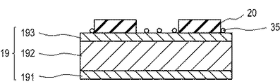
プロセスガスにおける酸化ガスの比率が比較高い場合、ハードマスク層をパターニングする際に、露出したバリアメタル層中のチタンと酸化ガスと反応して酸化チタン等の反応生成物が生成されることがある。図7は、ハードマスク層のパターニング後における反応生成物を示す概略断面図である。 When the ratio of the oxidizing gas in the process gas is relatively high, when patterning the hard mask layer, reaction products such as titanium oxide may be generated by reacting with titanium in the exposed barrier metal layer and the oxidizing gas. . FIG. 7 is a schematic cross-sectional view showing a reaction product after patterning of the hard mask layer.
図7に示すように、仮に酸化ガスの比率が比較的高いと、ハードマスク層20をパターニングする際に、露出したバリアメタル層193上に、バリアメタル層中のチタンと酸化ガスと反応して生成された酸化チタン等の反応生成物35が形成される。このような反応生成物35は、この後の洗浄工程におけるウェットエッチングのエッチングレートが低下する原因となる。なお、この洗浄工程は、バリアメタル層193上の反応生成物やエッチング残渣を含む異物を除去するためのものである。ウェットエッチングのエッチングレートが低下すると、異物をリフトオフすることが困難となり、その結果、配線ショートが発生して配線工程における歩留まりが低下することになる。
As shown in FIG. 7, if the ratio of the oxidizing gas is relatively high, when patterning the
これに対し、本実施形態に係る半導体装置の製造方法では、上記のようにプロセスガスにおける酸化ガスの比率を1%未満に低く抑える。これにより、バリアメタル層193における窒化チタン層中のチタンと酸化ガスとが反応して生成される反応生成物の発生を低減することができる。なお、酸化ガスの比率を低減するほど、反応生成物の発生を抑制する効果が大きくなる。また、微小な異物であっても配線ショートを引き起こす微細な金属配線ほど、反応生成物の抑制による配線ショートの発生を抑制する効果が顕著になる。
On the other hand, in the method for manufacturing a semiconductor device according to the present embodiment, the ratio of the oxidizing gas in the process gas is suppressed to less than 1% as described above. Thereby, generation | occurrence | production of the reaction product produced | generated when titanium in the titanium nitride layer in the
上記本実施形態におけるハードマスク層20のドライエッチングの条件は、適宜設定することができるが、例えば次のように設定することができる。
The conditions for dry etching of the
まず、ハードマスク層20直下のバリアメタル層193が露出しておらずプロセスガスに曝されていない状態では、ドライエッチングの条件を次のように設定することができる。まず、エッチング室内の圧力を10〜40mTorrに設定することができる。また、エッチング室内に導入するプロセスガスとして、CF4、CHF3、C4F8、及びArの混合ガスを用いることができる。また、CF4の流量を30〜120sccm、CHF3の流量を15〜60sccm、C4F8の流量を5〜20sccm、Arの流量を250〜1000sccmに設定することができる。
First, in a state where the
また、上記条件でエッチングが進行し、バリアメタル層193の窒化チタン層が露出してプロセスガスに曝された状態においては、オーバーエッチングとして行うドライエッチングの条件を次のように設定することができる。まず、エッチング室内の圧力を15〜60mTorrに設定することができる。また、エッチング室内に導入するプロセスガスとして、C4F8及びArの混合ガスを用いることができる。また、C4F8の流量を15〜60sccm、Arの流量を500〜2000sccmに設定することができる。
Further, in the state where the etching proceeds under the above conditions and the titanium nitride layer of the
上記のいずれの状態においても、酸素ガスは導入しないものとし、プロセスガスにおける酸化ガスの比率を1%未満とすることができる。上記いずれの状態においても酸素ガスを導入しないことにより、窒化チタン層中のチタンの酸化による反応生成物の発生をさらに低減することができる。なお、バリアメタル層193が露出しておらずプロセスガスに曝されていない状態では、必ずしもプロセスガスにおける酸化ガスの比率を1%未満とする必要はない。
In any of the above states, oxygen gas is not introduced, and the ratio of oxidizing gas in the process gas can be less than 1%. By not introducing oxygen gas in any of the above states, the generation of reaction products due to oxidation of titanium in the titanium nitride layer can be further reduced. In the state where the
なお、上記ドライエッチングの条件をオーバーエッチングの条件に変更するタイミングの決定には、エッチング室内の発光強度に基づきエッチング終点を検出する終点検出装置を用いることができる。すなわち、終点検出装置によりエッチング室内の発光強度をモニタし、そのモニタ結果に基づき、オーバーエッチングの条件に変更するタイミングを決定することができる。 Note that an end point detection device that detects the etching end point based on the emission intensity in the etching chamber can be used to determine the timing for changing the dry etching condition to the overetching condition. That is, the emission intensity in the etching chamber is monitored by the end point detection device, and the timing for changing to the overetching condition can be determined based on the monitoring result.
上記のようにして、ドライエッチングによりハードマスク層20をパターニングした後、例えばアッシング法を用いて、マスクとして用いたレジスト33を除去する(図6:工程S15)。
After the
次に、例えばアミン系の洗浄液を用いて洗浄を行い、洗浄液によりバリアメタル層193における窒化チタン層の露出した上部の一部をウェットエッチングする(図6:工程S16)。ここでアミン系の洗浄液とは、エタノールアミン、トリエタノールアミン、ヒドロキシルアミンなどアミンを含むものをいい、pH7以上の中性またはアルカリ性のものを指す。ウェットエッチングの条件としては、例えばエッチングレートを1〜2Å/分、エッチング時間を15〜60分間、具体的には30分間とすることができる。これにより、図4(a)に示すように、バリアメタル層193上に、パターニングされたハードマスク層20が形成される。なお、ここでのウェットエッチングに用いるエッチング液としての洗浄液は、上記アミン系の洗浄液に限定されるものではなく、エッチングレート、選択比等を考慮して種々のエッチング液から適宜選択することができる。
Next, cleaning is performed using, for example, an amine-based cleaning liquid, and a portion of the exposed upper portion of the titanium nitride layer in the
本実施形態では、上述のように、バリアメタル層193における窒化チタン層中のチタンと酸化ガスとが反応して生成される反応生成物の発生を低減することができる。したがって、上記のウェットエッチングにおけるエッチングレートの低下を抑制することができ、バリアメタル層193上の反応生成物やエッチング残渣を含む異物を十分に除去することができる。
In the present embodiment, as described above, it is possible to reduce the generation of reaction products generated by the reaction between titanium in the titanium nitride layer in the
なお、上記ウェットエッチングでは、窒化チタン層のエッチング量、すなわち窒化チタン層がエッチングされる厚さを好ましくは例えば50Å以上とすることができる。これにより、より効果的に反応生成物やエッチング残渣を含む異物を除去することができる。 In the wet etching, the etching amount of the titanium nitride layer, that is, the thickness at which the titanium nitride layer is etched can be preferably 50 mm or more, for example. Thereby, the foreign material containing a reaction product and an etching residue can be removed more effectively.
次に、パターニングされたハードマスク層20をエッチングマスクとして、例えばCl2系のガスでバリアメタル層193、導電層192、及びバリアメタル層191を順次ドライエッチングする(図6:工程S17)。ドライエッチングとしては、例えば反応性イオンエッチング等を用いることができる。これにより、バリアメタル層193、導電層192、及びバリアメタル層191をパターニングする。こうして、図4(b)に示すように、バリアメタル層191と導電層192とバリアメタル層193との積層膜よりなる第1の金属配線19が形成される。第1の金属配線19は、ほぼ垂直に側面が形成される。このとき、ハードマスク層20と第1の金属配線19を構成する各層との選択比は十分に確保されている。このため、ハードマスク層20の線幅はほぼ後退せずに、微細な第1の金属配線19を形成することができる。
Next, using the patterned
本実施形態によれば、第1の金属配線19のパターンにおいて隣接する配線間のスペースの幅d(図2参照)が例えば0.1〜0.2μm程度の非常に狭い箇所においても、配線間の短絡やリークの原因となりうる欠陥を十分に抑制できる。
According to the present embodiment, even in a very narrow portion where the width d (see FIG. 2) between adjacent wires in the pattern of the
なお、上記では、チタン層と窒化チタン層とが順次積層されてなるバリアメタル層191、193を用いているが、チタン層のない窒化チタン層よりなるバリアメタル層191、193を用いることもできる。
In the above description,
また、第1の金属配線19の導電層192を構成するAlCu合金層の配向を<111>方向に高めるように、AlCu合金層下のバリアメタル層191における窒化チタン層の配向を<111>方向に高めておいてもよい。これにより、AlCu合金層を有する第1の金属配線19の配線信頼性を向上することができる。
Further, the orientation of the titanium nitride layer in the
次に、第1の金属配線19が形成された層間絶縁層17上に、例えばプラズマCVD法により、厚さ約500nmのシリコン酸化層よりなる層間絶縁層21を成膜する(図6:工程S18)。層間絶縁層21を構成するシリコン酸化層は、例えば、約300〜400℃の成膜温度で、SiH4とO2とをプラズマ状態で反応させることにより成膜することができる。
Next, an
なお、層間絶縁層21は、第1の金属配線19の積層膜上のハードマスク層20を残したまま、第1の金属配線19の積層膜を含む表面上に形成される。
The interlayer insulating
次に、層間絶縁層21及びハードマスク層20に、第1の金属配線19に達するスルーホールを開口する。次いで、このスルーホールが形成された層間絶縁層21上に、例えばスパッタ法又はCVD法によりチタン層と窒化チタン層とが順次積層されてなるバリアメタル層を成膜し、続いて、例えばCVD法によりタングステン層を成膜する。次いで、層間絶縁層21上のバリアメタル層及びタングステン層を例えばCMP(Chemical Mechanical Polishing)法により除去し、スルーホール内にバリアメタル層及びタングステン層を埋め込む。こうして、図4(c)に示すように、スルーホール内に、バリアメタル層及びタングステン層よりなるビアプラグ22を埋め込む。
Next, a through hole reaching the
次に、層間絶縁層21上に、第1の金属配線19の場合と同様にして、第2の金属配線23を形成する。第2の金属配線23の場合も、第1の金属配線19の場合と同様に、シリコン酸化層よりなるハードマスク層24をマスクとして、ドライエッチングによりパターニングすることができる。また、第2の金属配線23も、上記第1の金属配線19と同様の構成を用いることができる。ハードマスク層24のドライエッチングにおいても、バリアメタル層233の窒化チタン層が露出してプロセスガスに曝された状態においては、プロセスガスにおける酸化ガスの比率を1%未満とするプロセスガスの比率の制御を実施する。
Next, the
次に、第2の金属配線23が形成された層間絶縁層21上に、例えばプラズマCVD法により、例えば厚さ約500nmのシリコン酸化層よりなる層間絶縁層25を成膜する。層間絶縁層25を構成するシリコン酸化層は、例えば、約300〜400℃の成膜温度で、SiH4とO2とをプラズマ状態で反応させることにより成膜することができる。
Next, an
次に、層間絶縁層25及びハードマスク層24に、第2の金属配線23に達するスルーホールを開口する。次いで、このスルーホールが形成された層間絶縁層25上に、例えばスパッタ法又はCVD法によりチタン層と窒化チタン層とが順次積層されてなるバリアメタル層を成膜し、続いて、例えばCVD法によりタングステン層を成膜する。次いで、層間絶縁層25上のバリアメタル層及びタングステン層を例えばCMP法により除去し、スルーホール内にバリアメタル層及びタングステン層を埋め込む。こうして、図5(a)に示すように、スルーホール内に、バリアメタル層及びタングステン層よりなるビアプラグ26を埋め込む。
Next, a through hole reaching the
次に、層間絶縁層25上に、例えばスパッタリング法により、例えばCuを約0.5wt%含んだAlCuよりなる厚さ約300nmのアルミニウム合金層を約300℃の成膜温度で成膜する。次いで、アルミニウム合金層上に、フォトリソグラフィによりレジストのマスクパターンを形成する。次に、レジストのマスクパターンをマスクとして、例えばCl2系のガスでアルミニウム合金層をドライエッチングし、アルミニウム合金層をパターニングする。ドライエッチングとしては、例えば反応性イオンエッチング等を用いることができる。こうして、ほぼ垂直に側面が形成されたアルミニウム合金層よりなる第3の金属配線27が形成される。上記により形成した第3の金属配線27においては、最小となる線幅を例えば0.25〜0.3μm程度とすることができる。
Next, an aluminum alloy layer having a thickness of about 300 nm made of AlCu containing, for example, about 0.5 wt% of Cu is formed on the
次に、第3の金属配線27が形成された層間絶縁層25上に、例えばプラズマCVD法により、例えば厚さ約500nmのシリコン酸化層よりなる層間絶縁層28を成膜する。層間絶縁層28を構成するシリコン酸化層は、例えば、約300〜400℃の成膜温度で、SiH4とO2とをプラズマ状態で反応させることにより成膜することができる。
Next, an
次に、層間絶縁層28に、第3の金属配線27に達するスルーホールを開口する。次いで、このスルーホールが形成された層間絶縁層28上に、例えばスパッタ法又はCVD法によりチタン層と窒化チタン層とが順次積層されてなるバリアメタル層を成膜し、続いて、例えばCVD法によりタングステン層を成膜する。次いで、層間絶縁層28上のバリアメタル層及びタングステン層を例えばCMP法により除去し、スルーホール内にバリアメタル層及びタングステン層を埋め込む。こうして、スルーホール内に、バリアメタル層及びタングステン層よりなるビアプラグ29を埋め込む。
Next, a through hole reaching the
次に、層間絶縁層28上に、例えばスパッタリング法により、例えばCuを約0.5wt%含んだAlCuよりなる厚さ約600nmのアルミニウム合金層を約300℃の成膜温度で成膜する。次いで、アルミニウム合金層上に、フォトリソグラフィによりレジストのマスクパターンを形成する。次に、レジストのマスクパターンをマスクとして、例えばCl2系のガスでアルミニウム合金層をドライエッチングし、アルミニウム合金層をパターニングする。ドライエッチングとしては、例えば反応性イオンエッチング等を用いることができる。こうして、ほぼ垂直に側面が形成されたアルミニウム合金層よりなる第4の金属配線30が形成される。第4の金属配線30には、ボンディングパッドが含まれる。上記により形成した第4の金属配線30においては、最小となる線幅を例えば0.5〜1.0μm程度とすることができる。
Next, an aluminum alloy layer having a thickness of about 600 nm made of AlCu containing, for example, about 0.5 wt% of Cu is formed on the
次に、第4の金属配線30が形成された層間絶縁層28上に、例えばプラズマCVD法により、例えば厚さ約500nmのシリコン窒化層よりなる保護絶縁膜31を成膜する。保護絶縁膜31を構成するシリコン窒化層は、例えば、約400〜430℃の成膜温度で、SiH4、N2、NH3を含むガスをプラズマ状態で反応させることにより成膜することができる。
Next, a protective insulating
次いで、保護絶縁膜31上に、フォトリソグラフィによりレジストのマスクパターンを形成する。次に、レジストのマスクパターンをマスクとして、例えばCF4系のガスでシリコン窒化層よりなる保護絶縁膜31をドライエッチングする。ドライエッチングとしては、例えば反応性イオンエッチング等を用いることができる。これにより、保護絶縁膜31に、第4の金属配線30のボンディングパッドに達する外部電極取り出し用の開口部32を開口する。
Next, a resist mask pattern is formed on the protective insulating
こうして、図5(b)に示すように、本実施形態に係る半導体装置が製造される。 Thus, as shown in FIG. 5B, the semiconductor device according to this embodiment is manufactured.
このように、本実施形態によれば、ハードマスク層をドライエッチングする際に、バリアメタル層の窒化チタン層が露出してプロセスガスに曝された状態においては、プロセスガスにおける酸化ガスの比率を1%未満とする。これにより、窒化チタン層中のチタンと酸化ガスとが反応して生成される反応生成物の生成を抑制することができる。この結果、ハードマスク層のドライエッチング後に続く洗浄工程において、窒化チタン層上の異物をウェットエッチングによりリフトオフして効率よく除去することができ、異物に起因する配線ショートの発生を抑制することができる。こうして、配線工程における歩留まりを向上することができる。 As described above, according to the present embodiment, when the hard mask layer is dry-etched, in the state where the titanium nitride layer of the barrier metal layer is exposed and exposed to the process gas, the ratio of the oxidizing gas in the process gas is increased. Less than 1%. Thereby, the production | generation of the reaction product produced | generated when titanium in a titanium nitride layer reacts with oxidizing gas can be suppressed. As a result, in the cleaning process subsequent to the dry etching of the hard mask layer, the foreign matter on the titanium nitride layer can be lifted off by wet etching and efficiently removed, and the occurrence of wiring shorts due to the foreign matter can be suppressed. . Thus, the yield in the wiring process can be improved.
以上のとおり、本実施形態によれば、ハードマスク層をマスクとして用いたドライエッチングにより金属配線の微細加工を実現するとともに、配線ショートの発生を抑制することができる。 As described above, according to the present embodiment, fine processing of metal wiring can be realized by dry etching using a hard mask layer as a mask, and occurrence of wiring short-circuit can be suppressed.
ここで、本願発明者が行った実験により得られたハードマスク層のドライエッチング時の酸素ガス濃度と反応生成物の有無及び配線歩留まりとの関係の例を表1に示す。なお、上記酸素ガス濃度とは、ドライエッチング時のプロセスガスの総流量に対する酸素ガスの流量の比率を意味する。表1によれば、上記酸素ガス濃度を1%未満とすることにより、反応生成物の発生が低減されるとともに、配線歩留まりが改善されることが分かる。

[第2の実施形態]
本発明の第2の実施形態に係る半導体装置の製造方法について説明する。なお、上記第1の実施形態に係る半導体装置及び半導体装置の製造方法と同一の構成要素については同一の符号を付し説明を省略し又は簡略にする。
[Second Embodiment]
A method for manufacturing a semiconductor device according to the second embodiment of the present invention will be described. Note that the same components as those of the semiconductor device and the method of manufacturing the semiconductor device according to the first embodiment are denoted by the same reference numerals, and description thereof is omitted or simplified.
上記第1の実施形態では、金属配線の形成に用いるハードマスク層のドライエッチングにおいて、バリアメタル層の窒化チタン層が露出してプロセスガスに曝された状態においては、プロセスガスにおける酸化ガスの比率を1%未満としていた。 In the first embodiment, in the dry etching of the hard mask layer used for forming the metal wiring, the ratio of the oxidizing gas in the process gas when the titanium nitride layer of the barrier metal layer is exposed and exposed to the process gas. Was less than 1%.
これに対し、本実施形態は、ハードマスク層のドライエッチングにおいて、バリアメタル層の窒化チタン層が露出してプロセスガスに曝された状態においては、プロセスガスにおける酸化ガスの比率を特に0%とする点で、第1の実施形態とは異なる。 In contrast, in the present embodiment, in the dry etching of the hard mask layer, in the state where the titanium nitride layer of the barrier metal layer is exposed and exposed to the process gas, the ratio of the oxidizing gas in the process gas is particularly 0%. This is different from the first embodiment.
例えば、第1の金属配線19の形成に用いるハードマスク層20を形成する際に、第1の実施形態の場合と同様に、例えばCF4系のガスでシリコン酸化層よりなるハードマスク層20をドライエッチングし、ハードマスク層20をパターニングする。その際、本実施形態では、バリアメタル層193の窒化チタン層が露出してプロセスガスに曝された状態においては、酸化ガスの比率を特に0%とするプロセスガスの比率の制御を実施する。
For example, when the
また、第2の金属配線23の形成に用いるハードマスク層24を形成する際にも同様に、バリアメタル層233の窒化チタン層が露出してプロセスガスに曝された状態においては、酸化ガスの比率を特に0%とするプロセスガスの比率の制御を実施する。
Similarly, when the
このように、本実施形態では、酸化ガスの比率を特に0%とすることより、窒化チタン層中のチタンと酸化ガスとが反応して生成される反応生成物の生成をさらに抑制することができ、配線ショートの発生をさらに抑制することができる。 As described above, in this embodiment, by setting the ratio of the oxidizing gas to particularly 0%, it is possible to further suppress the generation of the reaction product generated by the reaction between titanium and the oxidizing gas in the titanium nitride layer. This can further suppress the occurrence of wiring shorts.
[第3の実施形態]
本発明の第3の実施形態に係る半導体装置の製造方法について図8及び図9を参照して説明する。なお、上記第1の実施形態に係る半導体装置及び半導体装置の製造方法と同一の構成要素については同一の符号を付し説明を省略し又は簡略にする。
[Third Embodiment]
A method for manufacturing a semiconductor device according to the third embodiment of the present invention will be described with reference to FIGS. Note that the same components as those of the semiconductor device and the method of manufacturing the semiconductor device according to the first embodiment are denoted by the same reference numerals, and description thereof is omitted or simplified.
本実施形態は、金属配線の形成に用いるハードマスク層のドライエッチング後に続くウェットエッチングによる洗浄工程の後、金属配線となる積層膜のドライエッチングの前に、二流体洗浄により、露出したバリアメタル層の表面を洗浄する工程をさらに有する。この点で、本実施形態は、第1の実施形態とは異なる。 In the present embodiment, an exposed barrier metal layer is formed by two-fluid cleaning after a cleaning process by wet etching subsequent to dry etching of a hard mask layer used for forming a metal wiring and before dry etching of a laminated film to be a metal wiring. The method further includes a step of cleaning the surface. In this respect, the present embodiment is different from the first embodiment.
図8は、本実施形態に係る半導体装置の製造方法における第1の金属配線の形成工程を示すフローチャートである。図8に示す工程S21〜工程S26は、それぞれ上述した図6に示す工程S11〜工程S16と同様である。 FIG. 8 is a flowchart showing a first metal wiring forming step in the method for manufacturing a semiconductor device according to the present embodiment. Steps S21 to S26 shown in FIG. 8 are the same as Steps S11 to S16 shown in FIG.
本実施形態においても、第1の実施形態の場合と同様に、例えばCF4系のガスでハードマスク層20をドライエッチングし(図8:工程S24)、例えばアッシングによりレジスト33を除去する(図8:工程S25)。その後、例えばアミン系の洗浄液にてバリアメタル層193の窒化チタン層の一部をウェットエッチングする(図8:工程S26)。
Also in this embodiment, as in the case of the first embodiment, the
工程S26のウェットエッチングにおいて、窒化チタン層のウェットエッチング量が少ないと、窒化チタン層中のチタンと酸化ガスとの反応により生成される反応生成物が十分にリフトオフされないことがある。図9は、ウェットエッチングにより反応生成物が十分にリフトオフされていない状態を示す概略断面図である。図示するように、バリアメタル層193の窒化チタン層の上部の一部がウェットエッチングにより除去されているものの、反応生成物35がリフトオフされずに残存することがある。
In the wet etching in step S26, if the amount of wet etching of the titanium nitride layer is small, the reaction product generated by the reaction between titanium in the titanium nitride layer and the oxidizing gas may not be sufficiently lifted off. FIG. 9 is a schematic cross-sectional view showing a state where the reaction product is not sufficiently lifted off by wet etching. As shown in the drawing, although a part of the upper portion of the titanium nitride layer of the
そこで、本実施形態では、工程S26のウェットエッチングの後、例えば純水や窒素を用いた二流体洗浄により、バリアメタル層193の窒化チタン層の表面を洗浄する(図8:工程S27)。二流体洗浄による洗浄では、二流体ノズルにより、純水等の液体と窒素等の気体とを混合して微細霧として窒化チタン層の表面に噴射し、窒化チタン層の表面を洗浄する。
Therefore, in this embodiment, after the wet etching in step S26, the surface of the titanium nitride layer of the
なお、二流体洗浄に用いる液体及び気体は、それぞれ純水及び窒素に限定されるものではなく、必要とされる洗浄性等に応じて適宜選定することができる。また、二流体洗浄における液体及び気体の供給流量、二流体洗浄による洗浄時間等の条件についても、必要とされる洗浄性等に応じて適宜設定することができる。 The liquid and gas used for the two-fluid cleaning are not limited to pure water and nitrogen, respectively, and can be appropriately selected according to the required cleaning properties. Further, conditions such as the supply flow rate of liquid and gas in the two-fluid cleaning, the cleaning time by the two-fluid cleaning, and the like can be set as appropriate according to the required cleaning properties.
こうして、二流体洗浄により、工程S26で窒化チタン層のウェットエッチング量が少なくリフトオフされずに残存する反応生成物35を含む異物を効率的に除去することができる。これにより、異物に起因する配線ショートの発生を抑制し、配線工程における歩留まりを向上することができる。
In this way, the two-fluid cleaning can efficiently remove the foreign matter including the
二流体洗浄を行った後、上述した工程S17と同様に、ハードマスク層20をマスクとして、例えばCl2系のガスでバリアメタル層193、導電層192、及びバリアメタル層191をドライエッチングする(図8:工程S28)。これにより、第1の金属配線19を形成する。
After performing the two-fluid cleaning, the
層間絶縁層21を形成する工程(図8:工程S29)以後は、第1の実施形態と同様である。 Subsequent steps for forming the interlayer insulating layer 21 (FIG. 8: step S29) are the same as those in the first embodiment.
なお、第2の金属配線23の形成に用いるハードマスク層24を形成する際にも上記と同様に、ウェットエッチングによる洗浄工程の後、第2の金属配線23となる積層膜のドライエッチングの前に、二流体洗浄による洗浄を行うことができる。
In addition, when forming the
[第4の実施形態]
本発明の第4の実施形態に係る半導体装置の製造方法について図10を参照して説明する。なお、上記第1の実施形態に係る半導体装置及び半導体装置の製造方法と同一の構成要素については同一の符号を付し説明を省略し又は簡略にする。
[Fourth Embodiment]
A method for manufacturing a semiconductor device according to the fourth embodiment of the present invention will be described with reference to FIG. Note that the same components as those of the semiconductor device and the method of manufacturing the semiconductor device according to the first embodiment are denoted by the same reference numerals, and description thereof is omitted or simplified.
本実施形態では、金属配線の形成に用いるハードマスク層のドライエッチングのマスクとして用いるレジストの下に、反射防止層であるBARC(Bottom Anti Reflective Coating)が形成される。この点で、本実施形態は、第1の実施形態とは異なる。BARCを用いる本実施形態によれば、金属配線に加工される下地金属層による反射を抑えることでレジスト露光時のハレーションを抑制し、レジストのマスクパターンの精度を向上することができる。したがって、本実施形態によれば、マスクとして用いるハードマスク層の精度を向上することができ、さらに微細な配線加工を実現することができる。 In the present embodiment, BARC (Bottom Anti Reflective Coating), which is an antireflection layer, is formed under a resist used as a mask for dry etching of a hard mask layer used for forming metal wiring. In this respect, the present embodiment is different from the first embodiment. According to the present embodiment using BARC, it is possible to suppress halation during resist exposure by suppressing reflection by the underlying metal layer processed into the metal wiring, and to improve the accuracy of the resist mask pattern. Therefore, according to this embodiment, the accuracy of the hard mask layer used as a mask can be improved, and finer wiring processing can be realized.
さらに、本実施形態では、レジストのマスクパターンの形成後に露出したBARCをドライエッチングにより除去する工程が設けられ、このドライエッチングによりBARCを除去する工程を行う時間が特定の条件を満たすように規定されている。以下、本実施形態におけるBARCを除去する工程について図10を用いて説明する。図10は、本実施形態におけるBARCを除去する工程を説明する概略断面図である。 Further, in the present embodiment, a step of removing the BARC exposed after the formation of the resist mask pattern by dry etching is provided, and the time for performing the step of removing the BARC by dry etching is defined to satisfy a specific condition. ing. Hereinafter, the process of removing BARC in this embodiment will be described with reference to FIG. FIG. 10 is a schematic cross-sectional view for explaining the step of removing BARC in the present embodiment.
本実施形態では、バリアメタル層193上にハードマスク層20を形成した後、ハードマスク層20上にBARC36を塗布する。次いで、BARC36上にレジスト33を塗布した後、フォトリソグラフィにより、レジスト33をパターニングしてレジスト33のマスクパターンを形成する。BARC36上すなわち反射防止層上に形成されたレジスト33をフォトリソグラフィによりパターニングすることにより、下地金属層による反射が抑えられる結果、レジスト33の露光時のハレーションが抑制される。このため、レジスト33のマスクパターンの精度を向上することができる。
In the present embodiment, after the
次に、レジスト33をマスクとして、例えばCF4系のガスで、BARC36とシリコン酸化層よりなるハードマスク層20とをドライエッチングする。ドライエッチングとしては、例えば反応性イオンエッチング等を用いることができる。このとき、仮にプロセスガスにおける酸素ガス等の酸化系ガスの比率を1%未満とすると、BARC36のエッチングレートが低下する。この結果、図10(a)に示すように、BARC36が厚く形成されていたハードマスク層20上の凹部に、BARC36のエッチング残り36aが発生する懸念がある。BARC36のエッチング残り36aは、後工程のドライエッチングにおいてマスクとなるため、配線ショートの一因となるものである。
Next, using the resist 33 as a mask, the
そこで、本実施形態では、BARC36をドライエッチングにより除去する工程を設ける。そして、BARC36の厚さをA(nm)、BARC36のエッチングレートをB(nm/分)としたとき、BARC36をドライエッチングにより除去する工程を行う時間C(分)を、次の関係を満足するように設定する。
C≧(A/B)×1.5
Therefore, in this embodiment, a step of removing the
C ≧ (A / B) × 1.5
このように、本実施形態では、BARC36をドライエッチングにより除去する工程を十分な時間行う。これにより、図10(b)に示すように、ハードマスク層20上の凹部におけるBARC36のエッチング残り36aを除去又は低減することができる。
Thus, in this embodiment, the process of removing the
なお、BARC36のドライエッチングには、酸素ガス等の酸化ガスを用いることができる。これにより、BARC36のエッチングレートの低下を抑制して、BARCを除去する処理時間を短縮することができる。
Note that an oxidizing gas such as an oxygen gas can be used for dry etching of the
BARC36のドライエッチングの条件は、例えば次のように設定することができる。まず、エッチング室内の圧力を50〜200mTorrに設定することができる。また、エッチング室内に導入するプロセスガスとして、CF4及びO2の混合ガスを用いることができる。また、CF4の流量を75〜300sccm、O2の流量を10〜35sccmに設定することができる。
The conditions for dry etching of the
次に、第1の実施形態の場合と同様にして、レジスト33をマスクとして、例えばCF4系のガスでシリコン酸化層よりなるハードマスク層20をドライエッチングし、ハードマスク層20をパターニングする。ハードマスク層20のドライエッチングの条件は、第1の実施形態の場合と同様の条件を用いることができ、BARC36のドライエッチングとは異なり、プロセスガスに酸素ガス等の酸化ガスを用いないものとすることができる。
Next, as in the case of the first embodiment, the
次に、例えばアッシング法により、レジスト33及びBARC36を除去する。
Next, the resist 33 and the
以後、第1の実施形態の場合と同様にして、例えばアミン系の洗浄液を用いたウェットエッチングを行う。次いで、第1の実施形態の場合と同様にして、ハードマスク層20をエッチングマスクとして、例えばCl2系のガスでバリアメタル層193、導電層192、及びバリアメタル層191を順次ドライエッチングする。これにより、第1の金属配線19を形成する。
Thereafter, in the same manner as in the first embodiment, for example, wet etching using an amine-based cleaning liquid is performed. Next, as in the case of the first embodiment, using the
なお、第2の金属配線23の形成に用いるハードマスク層24を形成する際にも上記と同様に、BARCを用いることができる。
In addition, when forming the
このように、本実施形態によれば、BARCをドライエッチングにより除去する工程を十分な時間行うことにより、ハードマスク層の凹部等に残存するBARCのエッチング残りを低減することができる。しかも、BARCのドライエッチングには酸素ガス等の酸化系ガスを用いることにより、BARCを除去する処理時間を短縮することができる。したがって、ハードマスク層のエッチング時にプロセスガスにおける酸化ガスの比率を1%未満としたことによりBARCのエッチングレートが著しく小さくなる場合でも、BARCのエッチング残りがマスクになることを抑制することができる。これにより、配線ショートのリスクを軽減することができる。 As described above, according to the present embodiment, by performing the step of removing BARC by dry etching for a sufficient time, it is possible to reduce the etching residue of BARC remaining in the recesses of the hard mask layer. In addition, by using an oxidizing gas such as oxygen gas for the BARC dry etching, the processing time for removing the BARC can be shortened. Therefore, even when the etching rate of the BARC is significantly reduced by setting the ratio of the oxidizing gas in the process gas to less than 1% during the etching of the hard mask layer, it is possible to suppress the BARC etching residue from becoming a mask. Thereby, the risk of wiring short-circuit can be reduced.
[第5の実施形態]
本発明の第5の実施形態に係る半導体装置について図11を参照して説明する。なお、上記第1の実施形態に係る半導体装置と同一の構成要素については同一の符号を付し説明を省略し又は簡略にする。
[Fifth Embodiment]
A semiconductor device according to a fifth embodiment of the present invention will be described with reference to FIG. Note that the same components as those of the semiconductor device according to the first embodiment are denoted by the same reference numerals, and description thereof is omitted or simplified.
本実施形態は、ハードマスク層の下面の幅とバリアメタル層の下面の幅との関係の点で、第1の実施形態とは異なる。以下、本実施形態におけるハードマスク層の下面の幅とバリアメタル層の下面の幅との関係を含むハードマスク層及びバリアメタル層に関する構造的な特徴について説明する。 This embodiment is different from the first embodiment in terms of the relationship between the width of the lower surface of the hard mask layer and the width of the lower surface of the barrier metal layer. Hereinafter, structural features relating to the hard mask layer and the barrier metal layer including the relationship between the width of the lower surface of the hard mask layer and the width of the lower surface of the barrier metal layer in the present embodiment will be described.
図11は、本実施形態に係る半導体装置における金属配線を示す概略断面図であり、具体的には、第1の金属配線19の断面構造を示している。
FIG. 11 is a schematic cross-sectional view showing the metal wiring in the semiconductor device according to the present embodiment, and specifically shows the cross-sectional structure of the
図11に示すように、第1の金属配線19の上側のバリアメタル層193は、少なくともその上部において上面側から下面側に向かって徐々に幅広となるテーパ形状を有している。また、バリアメタル層193上のハードマスク層20も、少なくともその上部において上面側から下面側に向かって徐々に幅広となるテーパ形状を有している。
As shown in FIG. 11, the
ここで、ハードマスク層20の下面の幅をa(nm)、バリアメタル層193の上面の幅をb(nm)、バリアメタル層193の下面の幅をc(nm)とする。ハードマスク層20及びバリアメタル層193は、これらの幅a、b、及びcが次の大小関係を満足する構造的な特徴を有している。
c>a>b
Here, the width of the lower surface of the
c>a> b
すなわち、バリアメタル層193の下面の幅cが、ハードマスク層20の下面の幅aよりも広く、ハードマスク層20の下面の幅aが、バリアメタル層193の上面の幅bよりも広くなっている。
That is, the width c of the lower surface of the
上記図11に示す構造的な特徴も、図2に示す構造的な特徴と同様、ハードマスク層20をパターニングするためのドライエッチング後のウェットエッチングの際に生じたものである。すなわち、この構造的な特徴も、ハードマスク層20が除去されて露出したバリアメタル層193の上部の一部がウェットエッチングされて除去されるとともに、バリアメタル層193に対してサイドエッチングが入ることによるものである。本実施形態による半導体装置も上記第1の実施形態による半導体装置と同様にして製造することができるが、ウェットエッチングの条件により、上記図11に示すような構造的特徴が得られる。
The structural features shown in FIG. 11 are also generated during the wet etching after the dry etching for patterning the
[第6の実施形態]
本発明の第6の実施形態に係る半導体装置について図12を用いて説明する。図12は、本実施形態に係る半導体装置を示す概略図である。本実施形態では、本発明の半導体装置の一例である固体撮像装置について、その画素配列領域及び周辺領域を含む全体構成について説明する。
[Sixth Embodiment]
A semiconductor device according to a sixth embodiment of the present invention will be described with reference to FIG. FIG. 12 is a schematic view showing the semiconductor device according to the present embodiment. In this embodiment, an overall configuration including a pixel array region and a peripheral region of a solid-state imaging device which is an example of a semiconductor device of the present invention will be described.
図12に示すように、本実施形態に係る固体撮像装置800は、画素配列領域100および周辺領域700を有する。画素配列領域100は、複数の画素が配列される領域である。周辺領域700は、画素配列領域100の周辺に配された領域で、複数の画素を制御するための複数の制御回路や読み出し経路となる回路が配される領域である。
As illustrated in FIG. 12, the solid-
画素配列領域100には、複数の画素6が行方向および列方向に配列されている。各画素6は、光電変換部1、転送トランジスタ2、電荷電圧変換部FD、リセット部3、出力部4および選択部5を含む。光電変換部1は、図1に示すフォトダイオード拡散層15により構成される。また、転送トランジスタ2は、図1に示すゲート電極14を有するトランジスタである。また、電荷電圧変換部FDは、図1に示すソース/ドレイン拡散層16に接続される不純物拡散層であるフローティングディフュージョンである。
In the
また、周辺領域700には、複数の制御回路が配されている。複数の制御回路は、垂直走査回路500及び水平走査回路600を含む。また、複数の制御回路は、定電流源ブロック200、列アンプブロック300、保持容量ブロック400、及び出力アンプブロック450を含む。定電流源ブロック200は、画素配列領域100における複数の列に接続された複数の列信号線PVに対応して、複数の定電流源7を含む。列アンプブロック300は、複数の列信号線PVに対応して、複数の列アンプ部AMを含む。保持容量ブロック400は、複数の列アンプ部AMに対応して、複数の列信号保持部8を含む。出力アンプブロック450は、出力アンプ9を含む。
In the
11 シリコン基板
14 ゲート電極
15 フォトダイオード拡散層
16 ソース/ドレイン拡散層
17 層間絶縁層
18 コンタクトプラグ
19 第1の金属配線
191 バリアメタル層
192 導電層
193 バリアメタル層
20 ハードマスク層
21 層間絶縁層
22 ビアプラグ
23 第2の金属配線
231 バリアメタル層
232 導電層
233 バリアメタル層
24 ハードマスク層
33 レジスト
35 反応生成物
36 BARC
11
Claims (12)
前記バリアメタル層上にハードマスク層を形成する工程と、
前記ハードマスク層上にレジストをパターニングする工程と、
パターニングされた前記レジストをマスクとして前記ハードマスク層をドライエッチングし、前記ハードマスク層をパターニングする工程と、
前記ハードマスク層をパターニングする工程の後、前記バリアメタル層の表面を洗浄液で洗浄する工程と、
前記バリアメタル層の表面を洗浄する工程の後、パターニングされた前記ハードマスク層をマスクとして前記積層膜をドライエッチングする工程と
を有し、
前記ハードマスク層をパターニングする工程では、前記バリアメタル層がプロセスガスに曝された状態においては、前記プロセスガスの総流量に対する酸化ガスの流量の比率を1%未満としてドライエッチングすることを特徴とする半導体装置の製造方法。 Forming a laminated film having a conductive layer mainly composed of aluminum and a barrier metal layer formed on the conductive layer;
Forming a hard mask layer on the barrier metal layer;
Patterning a resist on the hard mask layer;
Dry etching the hard mask layer using the patterned resist as a mask, and patterning the hard mask layer;
After the step of patterning the hard mask layer, the step of cleaning the surface of the barrier metal layer with a cleaning liquid;
After the step of cleaning the surface of the barrier metal layer, the step of dry etching the laminated film using the patterned hard mask layer as a mask,
In the step of patterning the hard mask layer, when the barrier metal layer is exposed to a process gas, dry etching is performed with the ratio of the flow rate of the oxidizing gas to the total flow rate of the process gas being less than 1%. A method for manufacturing a semiconductor device.
前記レジストをパターニングする工程では、前記反射防止層上に形成された前記レジストをパターニングし、
前記レジストをパターニングする工程の後、前記ハードマスク層をパターニングする工程の前に、前記反射防止層をドライエッチングする工程を有することを特徴とする請求項1乃至5のいずれか1項に記載の半導体装置の製造方法。 Before the step of patterning the resist, the step of forming an antireflection layer on the barrier metal layer,
In the step of patterning the resist, the resist formed on the antireflection layer is patterned,
6. The method according to claim 1, further comprising a step of dry etching the antireflection layer after the step of patterning the resist and before the step of patterning the hard mask layer. A method for manufacturing a semiconductor device.
前記バリアメタル層上に形成されたハードマスク層とを有し、
前記ハードマスク層の下面の幅が、前記バリアメタル層の上面の幅よりも広く、
前記バリアメタル層の下面の幅が、前記バリアメタル層の上面の幅よりも広いことを特徴とする半導体装置。 A metal wiring having a conductive layer mainly composed of aluminum and a barrier metal layer formed on the conductive layer;
A hard mask layer formed on the barrier metal layer,
The width of the lower surface of the hard mask layer is wider than the width of the upper surface of the barrier metal layer,
The width of the lower surface of the barrier metal layer is wider than the width of the upper surface of the barrier metal layer.
Priority Applications (2)
| Application Number | Priority Date | Filing Date | Title |
|---|---|---|---|
| JP2015002052A JP2016127224A (en) | 2015-01-08 | 2015-01-08 | Semiconductor device and semiconductor device manufacturing method |
| US14/967,815 US9627319B2 (en) | 2015-01-08 | 2015-12-14 | Semiconductor device and semiconductor device manufacturing method using patterning and dry etching |
Applications Claiming Priority (1)
| Application Number | Priority Date | Filing Date | Title |
|---|---|---|---|
| JP2015002052A JP2016127224A (en) | 2015-01-08 | 2015-01-08 | Semiconductor device and semiconductor device manufacturing method |
Publications (2)
| Publication Number | Publication Date |
|---|---|
| JP2016127224A true JP2016127224A (en) | 2016-07-11 |
| JP2016127224A5 JP2016127224A5 (en) | 2018-02-15 |
Family
ID=56359761
Family Applications (1)
| Application Number | Title | Priority Date | Filing Date |
|---|---|---|---|
| JP2015002052A Pending JP2016127224A (en) | 2015-01-08 | 2015-01-08 | Semiconductor device and semiconductor device manufacturing method |
Country Status (2)
| Country | Link |
|---|---|
| US (1) | US9627319B2 (en) |
| JP (1) | JP2016127224A (en) |
Families Citing this family (3)
| Publication number | Priority date | Publication date | Assignee | Title |
|---|---|---|---|---|
| US10510598B2 (en) | 2016-11-29 | 2019-12-17 | Taiwan Semiconductor Manufacturing Company, Ltd. | Self-aligned spacers and method forming same |
| DE102017118475B4 (en) * | 2016-11-29 | 2022-08-25 | Taiwan Semiconductor Manufacturing Company, Ltd. | SELF-ALIGNED SPACERS AND METHOD OF MAKING THEM |
| JP6878154B2 (en) * | 2017-06-05 | 2021-05-26 | 東京エレクトロン株式会社 | Etching method and etching equipment |
Citations (7)
| Publication number | Priority date | Publication date | Assignee | Title |
|---|---|---|---|---|
| JP2001196376A (en) * | 2000-01-14 | 2001-07-19 | Seiko Epson Corp | Producing method for semiconductor device |
| JP2001210648A (en) * | 2000-01-28 | 2001-08-03 | Matsushita Electric Ind Co Ltd | Method of manufacturing electronic device |
| JP2001358145A (en) * | 2000-06-12 | 2001-12-26 | Matsushita Electric Ind Co Ltd | Wiring, method of forming the same, and semiconductor device |
| JP2006147846A (en) * | 2004-11-19 | 2006-06-08 | Renesas Technology Corp | Manufacturing method of semiconductor device |
| JP2009110986A (en) * | 2007-10-26 | 2009-05-21 | Tokyo Electron Ltd | Forming method of etching mask, control program, and program storage medium |
| JP2009277753A (en) * | 2008-05-13 | 2009-11-26 | Fujitsu Microelectronics Ltd | Manufacturing method of semiconductor device |
| JP2009295734A (en) * | 2008-06-04 | 2009-12-17 | Sharp Corp | Apparatus and method for manufacturing semiconductor device |
Family Cites Families (3)
| Publication number | Priority date | Publication date | Assignee | Title |
|---|---|---|---|---|
| KR100548515B1 (en) * | 2003-07-09 | 2006-02-02 | 매그나칩 반도체 유한회사 | method for forming metal line of semiconductor device |
| US7556989B2 (en) * | 2005-03-22 | 2009-07-07 | Samsung Electronics Co., Ltd. | Semiconductor device having fuse pattern and methods of fabricating the same |
| KR100703025B1 (en) * | 2005-07-05 | 2007-04-06 | 삼성전자주식회사 | Method for forming a metal wiring in semiconductor device |
-
2015
- 2015-01-08 JP JP2015002052A patent/JP2016127224A/en active Pending
- 2015-12-14 US US14/967,815 patent/US9627319B2/en active Active
Patent Citations (7)
| Publication number | Priority date | Publication date | Assignee | Title |
|---|---|---|---|---|
| JP2001196376A (en) * | 2000-01-14 | 2001-07-19 | Seiko Epson Corp | Producing method for semiconductor device |
| JP2001210648A (en) * | 2000-01-28 | 2001-08-03 | Matsushita Electric Ind Co Ltd | Method of manufacturing electronic device |
| JP2001358145A (en) * | 2000-06-12 | 2001-12-26 | Matsushita Electric Ind Co Ltd | Wiring, method of forming the same, and semiconductor device |
| JP2006147846A (en) * | 2004-11-19 | 2006-06-08 | Renesas Technology Corp | Manufacturing method of semiconductor device |
| JP2009110986A (en) * | 2007-10-26 | 2009-05-21 | Tokyo Electron Ltd | Forming method of etching mask, control program, and program storage medium |
| JP2009277753A (en) * | 2008-05-13 | 2009-11-26 | Fujitsu Microelectronics Ltd | Manufacturing method of semiconductor device |
| JP2009295734A (en) * | 2008-06-04 | 2009-12-17 | Sharp Corp | Apparatus and method for manufacturing semiconductor device |
Also Published As
| Publication number | Publication date |
|---|---|
| US9627319B2 (en) | 2017-04-18 |
| US20160204068A1 (en) | 2016-07-14 |
Similar Documents
| Publication | Publication Date | Title |
|---|---|---|
| KR100600689B1 (en) | Manufacturing method of semiconductor device | |
| JP2006216854A (en) | Manufacturing method for semiconductor device | |
| CN110600388A (en) | Method for improving crystallization defect of aluminum bonding pad | |
| KR101030299B1 (en) | Semiconductor device and method for manufacturing the device | |
| US9627319B2 (en) | Semiconductor device and semiconductor device manufacturing method using patterning and dry etching | |
| US9287228B2 (en) | Method for etching semiconductor structures and etching composition for use in such a method | |
| JP2007123548A (en) | Manufacturing method for semiconductor device | |
| US7384823B2 (en) | Method for manufacturing a semiconductor device having a stabilized contact resistance | |
| US8253254B2 (en) | Semiconductor device and manufacturing method thereof | |
| US20180331044A1 (en) | Semiconductor device and fabrication method thereof | |
| US7622331B2 (en) | Method for forming contacts of semiconductor device | |
| JP2010118661A (en) | Image sensor and method of manufacturing the image sensor | |
| US20180350663A1 (en) | Method of forming semiconductor device | |
| JP2006148052A (en) | Method for forming storage electrode of semiconductor element | |
| KR100814259B1 (en) | Method of manufacturing semiconductor device | |
| US6576563B2 (en) | Method of manufacturing a semiconductor device employing a fluorine-based etch substantially free of hydrogen | |
| KR101043734B1 (en) | Method for fabrication of semiconductor device | |
| KR100701779B1 (en) | Method for fabricating contact of semiconductor device | |
| US7901976B1 (en) | Method of forming borderless contacts | |
| CN114695252A (en) | Method for forming metal layer | |
| KR100802311B1 (en) | Method for fabricating cmos image sensor | |
| KR20090056333A (en) | Image sensor and method for manufacturing the sensor | |
| KR100639205B1 (en) | Method of manufacturing semiconductor device | |
| JP2006210436A (en) | Method of manufacturing ferroelectric capacitor | |
| TWI524377B (en) | Method for manufacturing semiconductor integrated circuit |
Legal Events
| Date | Code | Title | Description |
|---|---|---|---|
| RD05 | Notification of revocation of power of attorney |
Free format text: JAPANESE INTERMEDIATE CODE: A7425 Effective date: 20171214 |
|
| A521 | Request for written amendment filed |
Free format text: JAPANESE INTERMEDIATE CODE: A523 Effective date: 20180105 |
|
| A621 | Written request for application examination |
Free format text: JAPANESE INTERMEDIATE CODE: A621 Effective date: 20180105 |
|
| RD04 | Notification of resignation of power of attorney |
Free format text: JAPANESE INTERMEDIATE CODE: A7424 Effective date: 20180126 |
|
| A977 | Report on retrieval |
Free format text: JAPANESE INTERMEDIATE CODE: A971007 Effective date: 20180928 |
|
| A131 | Notification of reasons for refusal |
Free format text: JAPANESE INTERMEDIATE CODE: A131 Effective date: 20181101 |
|
| A521 | Request for written amendment filed |
Free format text: JAPANESE INTERMEDIATE CODE: A523 Effective date: 20181226 |
|
| A02 | Decision of refusal |
Free format text: JAPANESE INTERMEDIATE CODE: A02 Effective date: 20190530 |