JP2016015252A - 電子顕微鏡装置およびそれを用いた撮像方法 - Google Patents
電子顕微鏡装置およびそれを用いた撮像方法 Download PDFInfo
- Publication number
- JP2016015252A JP2016015252A JP2014136874A JP2014136874A JP2016015252A JP 2016015252 A JP2016015252 A JP 2016015252A JP 2014136874 A JP2014136874 A JP 2014136874A JP 2014136874 A JP2014136874 A JP 2014136874A JP 2016015252 A JP2016015252 A JP 2016015252A
- Authority
- JP
- Japan
- Prior art keywords
- image
- field
- narrow
- wide
- region
- Prior art date
- Legal status (The legal status is an assumption and is not a legal conclusion. Google has not performed a legal analysis and makes no representation as to the accuracy of the status listed.)
- Granted
Links
Images


Classifications
-
- H—ELECTRICITY
- H01—ELECTRIC ELEMENTS
- H01J—ELECTRIC DISCHARGE TUBES OR DISCHARGE LAMPS
- H01J37/00—Discharge tubes with provision for introducing objects or material to be exposed to the discharge, e.g. for the purpose of examination or processing thereof
- H01J37/26—Electron or ion microscopes; Electron or ion diffraction tubes
- H01J37/261—Details
- H01J37/265—Controlling the tube; circuit arrangements adapted to a particular application not otherwise provided, e.g. bright-field-dark-field illumination
-
- H—ELECTRICITY
- H01—ELECTRIC ELEMENTS
- H01J—ELECTRIC DISCHARGE TUBES OR DISCHARGE LAMPS
- H01J37/00—Discharge tubes with provision for introducing objects or material to be exposed to the discharge, e.g. for the purpose of examination or processing thereof
- H01J37/02—Details
- H01J37/244—Detectors; Associated components or circuits therefor
-
- H—ELECTRICITY
- H01—ELECTRIC ELEMENTS
- H01J—ELECTRIC DISCHARGE TUBES OR DISCHARGE LAMPS
- H01J37/00—Discharge tubes with provision for introducing objects or material to be exposed to the discharge, e.g. for the purpose of examination or processing thereof
- H01J37/26—Electron or ion microscopes; Electron or ion diffraction tubes
- H01J37/261—Details
- H01J37/263—Contrast, resolution or power of penetration
-
- H—ELECTRICITY
- H01—ELECTRIC ELEMENTS
- H01J—ELECTRIC DISCHARGE TUBES OR DISCHARGE LAMPS
- H01J37/00—Discharge tubes with provision for introducing objects or material to be exposed to the discharge, e.g. for the purpose of examination or processing thereof
- H01J37/26—Electron or ion microscopes; Electron or ion diffraction tubes
- H01J37/28—Electron or ion microscopes; Electron or ion diffraction tubes with scanning beams
-
- H—ELECTRICITY
- H01—ELECTRIC ELEMENTS
- H01J—ELECTRIC DISCHARGE TUBES OR DISCHARGE LAMPS
- H01J2237/00—Discharge tubes exposing object to beam, e.g. for analysis treatment, etching, imaging
- H01J2237/22—Treatment of data
- H01J2237/221—Image processing
-
- H—ELECTRICITY
- H01—ELECTRIC ELEMENTS
- H01J—ELECTRIC DISCHARGE TUBES OR DISCHARGE LAMPS
- H01J2237/00—Discharge tubes exposing object to beam, e.g. for analysis treatment, etching, imaging
- H01J2237/245—Detection characterised by the variable being measured
- H01J2237/24592—Inspection and quality control of devices
-
- H—ELECTRICITY
- H01—ELECTRIC ELEMENTS
- H01J—ELECTRIC DISCHARGE TUBES OR DISCHARGE LAMPS
- H01J2237/00—Discharge tubes exposing object to beam, e.g. for analysis treatment, etching, imaging
- H01J2237/26—Electron or ion microscopes
- H01J2237/28—Scanning microscopes
- H01J2237/2809—Scanning microscopes characterised by the imaging problems involved
-
- H—ELECTRICITY
- H01—ELECTRIC ELEMENTS
- H01J—ELECTRIC DISCHARGE TUBES OR DISCHARGE LAMPS
- H01J2237/00—Discharge tubes exposing object to beam, e.g. for analysis treatment, etching, imaging
- H01J2237/26—Electron or ion microscopes
- H01J2237/28—Scanning microscopes
- H01J2237/2813—Scanning microscopes characterised by the application
- H01J2237/2817—Pattern inspection
Landscapes
- Chemical & Material Sciences (AREA)
- Analytical Chemistry (AREA)
- Image Processing (AREA)
- Microscoopes, Condenser (AREA)
Abstract
【解決手段】電子顕微鏡装置を用いた撮像方法において、試料の広視野領域に収束させた電子ビームを低ドーズ量で照射し走査して試料の広視野画像を取得し、この広視野画像から広視野領域の内部に含まれる比較的狭い視野の狭視野領域を設定し、この狭視野領域に収束させた電子ビームを高ドーズ量で照射し走査して試料の狭視野画像を取得し、取得した広視野画像と狭視野画像とのノイズ除去パラメータを画素あたりのドーズ量に応じて決定し、このノイズ除去パラメータに基づいて広視野画像と狭視野画像の画質改善処理を行い、この画質改善処理を施した広視野画像を用いて画質改善処理を施した狭視野画像のドリフト補正を行い、このドリフト補正を行った狭視野画像と広視野画像とを合成画像の全領域における視認性が同程度となるよう合成するようにした。
【選択図】 図1
Description
以下に、本発明に係る実施の形態について図面を用いて説明する。
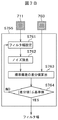
図1は、本発明の一実施形態である走査型電子顕微鏡装置100の基本構成である。走査電子顕微鏡装置100は、例えば、走査型電子顕微鏡101、入出力部121、制御部122、処理部123、記憶部124、画像処理部125を備えて構成される。
Claims (16)
- 試料に収束させた電子ビームを照射し前記試料の画像を取得する電子顕微鏡において、
前記試料の画像を取得するための処理条件を設定する処理部と、
前記取得した前記試料の画像を処理する画像処理部と、
前記試料の画像を取得するための条件を入力し、前記画像処理部で処理した結果を出力する入出力部と、
前記画像処理部と前記入出力部とを制御する制御部とを備え、
前記画像処理部は、
前記試料の画像を取得するための比較的広い視野の広視野領域と、該広視野領域の内部に含まれる1つ以上の比較的狭い視野の狭視野領域とを設定し、前記広視野領域と前記狭視野領域とを撮像して取得する広視野画像と狭視野画像の画素あたりのドーズ量が前記広視野画像よりも前記狭視野画像のほうが多くなるように設定する撮像領域設定部と、
前記広視野領域と前記狭視野領域との画質改善処理に関するパラメータを各領域の画素あたりのドーズ量に応じて決定するパラメータ決定部と、
該パラメータ決定部で決定したパラメータに基づいて前記広視野画像と狭視野画像との画質改善処理を行う画質改善処理部と、
該画質改善処理部で画質改善処理して画像を合成する画像合成部と
を有することを特徴とする電子顕微鏡装置。 - 前記撮像領域設定部は、ユーザ入力,前記電子顕微鏡で取得した前記狭視野画像または前記広視野画像中の輝度値の変化から判定した構造物情報のうち1つ以上の情報に基づいて前記広視野領域または前記狭視野領域を設定することを特徴とする請求項1記載の電子顕微鏡装置。
- 前記処理部は、前記試料の画像を取得するための処理条件として、ユーザ入力,前記構造物情報のうち1つ以上の情報に基づき、前記撮像領域設定部で設定した前記広視野領域と前記狭視野領域における前記ドーズ量,倍率,走査方法に関する撮像条件を設定することを特徴とする請求項1記載の電子顕微鏡装置。
- 前記撮像領域設定部は、前記画質改善処理部で画質改善した前記狭視野画像または広視野画像中の輝度変化から画像中の構造物情報を判定することを特徴とする請求項2記載の電子顕微鏡装置。
- 前記パラメータ決定部は、ノイズ除去の強度に基づいて、合成画像の各領域における画質改善処理のパラメータを設定することを特徴とする請求項1記載の電子顕微鏡装置。
- 前記画像合成部は、前記広視野画像,前記構造物情報,前記広視野画像と狭視野画像の合成途中画像のうちの1つ以上の情報を用いて、1つ以上の前記狭視画像をドリフト補正することを特徴とする請求項1記載の電子顕微鏡装置。
- 前記パラメータ決定部は、前記広視野画像と1つ以上の前記狭視野画像の合成画像の全領域におけるノイズ度合が同程度となるようパラメータを決定することを特徴とする請求項1記載の電子顕微鏡装置。
- 試料に収束させた電子ビームを照射し前記試料の画像を取得する電子顕微鏡装置を用いた撮像方法であって、
試料の画像を取得するための初期条件を設定し、
該設定した初期条件に基づいて前記試料の広視野領域と前記広視野領域の内部に含まれる1つ以上の比較的狭い狭視野領域を設定し、
前記広視野領域と前記狭視野領域とを撮像して取得する広視野画像と狭視野画像の画素あたりのドーズ量が前記広視野画像よりも前記狭視野画像のほうが多くなるように設定し、
前記撮像して取得する前記広視野領域と狭視野領域との画像の画質改善パラメータを各領域の画素あたりのドーズ量に応じて決定し、
該決定した画質改善パラメータを用いて、前記広視野領域と狭視野領域との画像の画質改善処理を行い、
該画質改善処理を行った前記広視野領域と狭視野領域との画像を合成する
ことを特徴とする電子顕微鏡装置を用いた撮像方法。 - ユーザ入力,前記電子顕微鏡で取得した前記狭視野画像または前記広視野画像中の輝度値の変化から判定した構造物情報のうち1つ以上の情報に基づいて前記広視野領域または前記狭視野領域を設定することを特徴とする請求項8記載の電子顕微鏡装置を用いた撮像方法。
- 前記試料の画像を取得するための処理条件として、ユーザ入力,前記構造物情報のうち1つ以上の情報に基づき、前記設定した前記広視野領域と前記狭視野領域における前記ドーズ量,倍率,走査方法に関する撮像条件を設定することを特徴とする請求項8記載の電子顕微鏡装置を用いた撮像方法。
- 画質改善した前記狭視野画像または広視野画像中の輝度変化から画像中の構造物情報を判定することを特徴とする請求項9記載の電子顕微鏡装置を用いた撮像方法。
- ノイズ除去の強度に基づいて、合成画像の各領域における画質改善処理のパラメータを設定することを特徴とする請求項8記載の電子顕微鏡装置を用いた撮像方法。
- 前記広視野画像と狭視野画像とを合成する工程において、前記広視野画像,前記構造物情報,前記広視野画像と狭視野画像の合成途中画像のうちの1つ以上の情報を用いて、1つ以上の前記狭視画像をドリフト補正することを特徴とする請求項8記載の電子顕微鏡装置を用いた撮像方法。
- 前記画質改善パラメータを、前記広視野画像と1つ以上の前記狭視野画像の合成画像の全領域におけるノイズ度合が同程度となるよう決定することを特徴とする請求項8記載の電子顕微鏡装置を用いた撮像方法。
- 前記試料の広視野領域及び該広視野領域に含まれる狭視野領域に収束させた電子ビームを前記狭視野領域には比較的高ドーズ量で照射し前記狭視野領域以外の前記広視野領域には比較的低ドーズ量で照射することにより前記試料の狭視野画像を含む広視野画像をフレーム画像として取得し、
該取得したフレーム画像の画質改善処理を行い、
該画質改善処理を施したフレーム画像について複数枚の画像をドリフト補正してフレーム加算する
ことを特徴とする電子顕微鏡装置を用いた撮像方法。 - 前記取得した複数のフレーム画像の撮像において、前記構造物情報に応じて狭視野領域の設定を変更することを特徴とする請求項15記載の電子顕微鏡装置を用いた撮像方法。
Priority Applications (5)
| Application Number | Priority Date | Filing Date | Title |
|---|---|---|---|
| JP2014136874A JP6190768B2 (ja) | 2014-07-02 | 2014-07-02 | 電子顕微鏡装置およびそれを用いた撮像方法 |
| PCT/JP2015/065319 WO2016002397A1 (ja) | 2014-07-02 | 2015-05-27 | 電子顕微鏡装置およびそれを用いた撮像方法 |
| US15/312,866 US9824853B2 (en) | 2014-07-02 | 2015-05-27 | Electron microscope device and imaging method using same |
| DE112015001902.2T DE112015001902B4 (de) | 2014-07-02 | 2015-05-27 | Elektronenmikroskopvorrichtung und sie verwendendes Abbildungsverfahren |
| CN201580027482.2A CN106415774B (zh) | 2014-07-02 | 2015-05-27 | 电子显微镜装置及使用该电子显微镜装置的拍摄方法 |
Applications Claiming Priority (1)
| Application Number | Priority Date | Filing Date | Title |
|---|---|---|---|
| JP2014136874A JP6190768B2 (ja) | 2014-07-02 | 2014-07-02 | 電子顕微鏡装置およびそれを用いた撮像方法 |
Publications (3)
| Publication Number | Publication Date |
|---|---|
| JP2016015252A true JP2016015252A (ja) | 2016-01-28 |
| JP2016015252A5 JP2016015252A5 (ja) | 2016-12-22 |
| JP6190768B2 JP6190768B2 (ja) | 2017-08-30 |
Family
ID=55018950
Family Applications (1)
| Application Number | Title | Priority Date | Filing Date |
|---|---|---|---|
| JP2014136874A Expired - Fee Related JP6190768B2 (ja) | 2014-07-02 | 2014-07-02 | 電子顕微鏡装置およびそれを用いた撮像方法 |
Country Status (5)
| Country | Link |
|---|---|
| US (1) | US9824853B2 (ja) |
| JP (1) | JP6190768B2 (ja) |
| CN (1) | CN106415774B (ja) |
| DE (1) | DE112015001902B4 (ja) |
| WO (1) | WO2016002397A1 (ja) |
Cited By (3)
| Publication number | Priority date | Publication date | Assignee | Title |
|---|---|---|---|---|
| KR20230010760A (ko) * | 2020-07-14 | 2023-01-19 | 주식회사 히타치하이테크 | 시료상 관찰 장치 및 그 방법 |
| WO2024157405A1 (ja) * | 2023-01-26 | 2024-08-02 | 株式会社日立ハイテク | 荷電粒子線装置、画像処理方法および画像処理プログラム |
| JP2024150622A (ja) * | 2020-01-09 | 2024-10-23 | 株式会社日立ハイテク | 画像を生成するシステム、及び非一時的コンピュータ可読媒体 |
Families Citing this family (10)
| Publication number | Priority date | Publication date | Assignee | Title |
|---|---|---|---|---|
| EP3183612A4 (en) * | 2014-08-18 | 2018-06-27 | ViewsIQ Inc. | System and method for embedded images in large field-of-view microscopic scans |
| CN107847839B (zh) * | 2015-08-21 | 2020-05-29 | 康明斯过滤Ip公司 | 高速旋转曲轴箱通风过滤介质和介质包 |
| CN111001225B (zh) | 2015-08-28 | 2021-11-19 | 康明斯过滤Ip公司 | 具有定向的液体排放口和气体出口的旋转聚结元件 |
| JP6391170B2 (ja) * | 2015-09-03 | 2018-09-19 | 東芝メモリ株式会社 | 検査装置 |
| US10096097B2 (en) * | 2016-08-01 | 2018-10-09 | The United States Of America As Represented By The Secretary Of The Navy | Content-aware bidirectional image edge highlighting |
| JP7107653B2 (ja) * | 2017-08-31 | 2022-07-27 | 東レエンジニアリング先端半導体Miテクノロジー株式会社 | 画像生成方法 |
| JP7171010B2 (ja) * | 2018-03-07 | 2022-11-15 | 株式会社日立ハイテクサイエンス | 断面加工観察装置、断面加工観察方法及びプログラム |
| EP3598474A1 (en) | 2018-07-19 | 2020-01-22 | FEI Company | Adaptive specimen image acquisition using an artificial neural network |
| CN109087293B (zh) * | 2018-07-27 | 2020-10-16 | 新华三大数据技术有限公司 | 一种调节电子显微镜成像参数的方法及装置 |
| WO2020198752A1 (en) | 2019-03-28 | 2020-10-01 | Massachusetts Institute Of Technology | System and method for learning-guided electron microscopy |
Citations (3)
| Publication number | Priority date | Publication date | Assignee | Title |
|---|---|---|---|---|
| JPH0562630A (ja) * | 1991-08-30 | 1993-03-12 | Jeol Ltd | 複数の記録位置を備えた電子顕微鏡 |
| JP2012032205A (ja) * | 2010-07-29 | 2012-02-16 | Hitachi High-Technologies Corp | 検査方法及び装置 |
| JP2012226874A (ja) * | 2011-04-15 | 2012-11-15 | Ccs Inc | 反射型照明装置 |
Family Cites Families (12)
| Publication number | Priority date | Publication date | Assignee | Title |
|---|---|---|---|---|
| SG92679A1 (en) * | 2000-02-29 | 2002-11-19 | Inst Materials Research & Eng | Selective deposition of a particle beam based on charging characteristics of a sample |
| KR100443143B1 (ko) * | 2000-03-06 | 2004-08-04 | 올림푸스 가부시키가이샤 | 섹셔닝상 관찰장치에 적용되는 패턴형성부재 및 그것을이용한 섹셔닝상 관찰장치 |
| US7634061B1 (en) * | 2004-03-26 | 2009-12-15 | Nova R & D, Inc. | High resolution imaging system |
| JP2011033423A (ja) * | 2009-07-31 | 2011-02-17 | Hitachi High-Technologies Corp | パターン形状選択方法、及びパターン測定装置 |
| JP5188529B2 (ja) * | 2010-03-30 | 2013-04-24 | 株式会社日立ハイテクノロジーズ | 電子ビーム照射方法、及び走査電子顕微鏡 |
| JP5537460B2 (ja) * | 2011-02-17 | 2014-07-02 | 株式会社日立ハイテクノロジーズ | 荷電粒子線顕微鏡及びそれを用いた計測画像の補正方法 |
| JP5537488B2 (ja) * | 2011-04-15 | 2014-07-02 | 株式会社日立ハイテクノロジーズ | 荷電粒子顕微鏡装置および画像撮像方法 |
| WO2012155267A1 (en) * | 2011-05-13 | 2012-11-22 | Fibics Incorporated | Microscopy imaging method and system |
| JP5712074B2 (ja) * | 2011-07-20 | 2015-05-07 | 株式会社日立ハイテクノロジーズ | 走査透過電子顕微鏡 |
| JP2014029460A (ja) * | 2012-07-05 | 2014-02-13 | Canon Inc | 顕微鏡装置及びその制御方法 |
| US9390887B2 (en) * | 2013-09-17 | 2016-07-12 | Kla-Tencor Corporation | Non-invasive charged particle beam monitor |
| JP6242745B2 (ja) * | 2014-05-13 | 2017-12-06 | 株式会社日立ハイテクノロジーズ | 荷電粒子線装置及び当該装置を用いる検査方法 |
-
2014
- 2014-07-02 JP JP2014136874A patent/JP6190768B2/ja not_active Expired - Fee Related
-
2015
- 2015-05-27 US US15/312,866 patent/US9824853B2/en not_active Expired - Fee Related
- 2015-05-27 DE DE112015001902.2T patent/DE112015001902B4/de not_active Expired - Fee Related
- 2015-05-27 CN CN201580027482.2A patent/CN106415774B/zh active Active
- 2015-05-27 WO PCT/JP2015/065319 patent/WO2016002397A1/ja not_active Ceased
Patent Citations (3)
| Publication number | Priority date | Publication date | Assignee | Title |
|---|---|---|---|---|
| JPH0562630A (ja) * | 1991-08-30 | 1993-03-12 | Jeol Ltd | 複数の記録位置を備えた電子顕微鏡 |
| JP2012032205A (ja) * | 2010-07-29 | 2012-02-16 | Hitachi High-Technologies Corp | 検査方法及び装置 |
| JP2012226874A (ja) * | 2011-04-15 | 2012-11-15 | Ccs Inc | 反射型照明装置 |
Cited By (6)
| Publication number | Priority date | Publication date | Assignee | Title |
|---|---|---|---|---|
| JP2024150622A (ja) * | 2020-01-09 | 2024-10-23 | 株式会社日立ハイテク | 画像を生成するシステム、及び非一時的コンピュータ可読媒体 |
| JP7660753B2 (ja) | 2020-01-09 | 2025-04-11 | 株式会社日立ハイテク | 画像を生成するシステム、及び非一時的コンピュータ可読媒体 |
| KR20230010760A (ko) * | 2020-07-14 | 2023-01-19 | 주식회사 히타치하이테크 | 시료상 관찰 장치 및 그 방법 |
| KR102831613B1 (ko) * | 2020-07-14 | 2025-07-09 | 주식회사 히타치하이테크 | 시료상 관찰 장치 및 그 방법 |
| US12431325B2 (en) | 2020-07-14 | 2025-09-30 | Hitachi High-Tech Corporation | Sample image observation device and method for same |
| WO2024157405A1 (ja) * | 2023-01-26 | 2024-08-02 | 株式会社日立ハイテク | 荷電粒子線装置、画像処理方法および画像処理プログラム |
Also Published As
| Publication number | Publication date |
|---|---|
| US9824853B2 (en) | 2017-11-21 |
| CN106415774A (zh) | 2017-02-15 |
| CN106415774B (zh) | 2017-12-15 |
| JP6190768B2 (ja) | 2017-08-30 |
| DE112015001902B4 (de) | 2021-01-21 |
| WO2016002397A1 (ja) | 2016-01-07 |
| US20170169992A1 (en) | 2017-06-15 |
| DE112015001902T5 (de) | 2017-02-02 |
Similar Documents
| Publication | Publication Date | Title |
|---|---|---|
| JP6190768B2 (ja) | 電子顕微鏡装置およびそれを用いた撮像方法 | |
| JP2014207110A (ja) | 観察装置および観察方法 | |
| JP5422673B2 (ja) | 荷電粒子線顕微鏡及びそれを用いた測定方法 | |
| US10623627B2 (en) | System for generating a synthetic 2D image with an enhanced depth of field of a biological sample | |
| JP5164754B2 (ja) | 走査型荷電粒子顕微鏡装置及び走査型荷電粒子顕微鏡装置で取得した画像の処理方法 | |
| JP5537488B2 (ja) | 荷電粒子顕微鏡装置および画像撮像方法 | |
| JP2007334892A (ja) | デジタルグレー値画像の処理方法 | |
| JP6099477B2 (ja) | 撮像装置、顕微鏡システム及び撮像方法 | |
| JP4857101B2 (ja) | プローブ評価方法 | |
| CN105981129B (zh) | 扫描带电粒子显微镜图像的高画质化方法和扫描带电粒子显微镜装置 | |
| JP5775948B2 (ja) | 荷電粒子顕微鏡装置および画像撮像方法 | |
| JP7701601B2 (ja) | 鋼板中の磁区観察方法 | |
| JP2016033857A (ja) | 走査荷電粒子顕微鏡画像の高画質化方法およびその装置 | |
| CN110389140A (zh) | 实现元素空间定位的双能焦点堆栈三维重构方法 | |
| US11256078B2 (en) | Continuous scanning for localization microscopy | |
| Mehendale et al. | Image fusion using adaptive thresholding and cross filtering | |
| US9396906B2 (en) | Transmission electron microscope and method of displaying TEM images | |
| Chantara et al. | Focus Measure of light field image using modified Laplacian and weighted harmonic variance | |
| JP2009277618A (ja) | 磁区構造画像取得方法および走査透過電子顕微鏡 | |
| JP2004117208A (ja) | パターン計測装置、パターン計測方法およびプログラム | |
| ABD HALIM et al. | Multiple Smoothing and Morphological Techniques in Radiographic Image Enhancement | |
| CN105939471A (zh) | 图像处理装置、摄像装置以及图像处理方法 |
Legal Events
| Date | Code | Title | Description |
|---|---|---|---|
| A521 | Request for written amendment filed |
Free format text: JAPANESE INTERMEDIATE CODE: A523 Effective date: 20161107 |
|
| A621 | Written request for application examination |
Free format text: JAPANESE INTERMEDIATE CODE: A621 Effective date: 20161107 |
|
| TRDD | Decision of grant or rejection written | ||
| A01 | Written decision to grant a patent or to grant a registration (utility model) |
Free format text: JAPANESE INTERMEDIATE CODE: A01 Effective date: 20170725 |
|
| A61 | First payment of annual fees (during grant procedure) |
Free format text: JAPANESE INTERMEDIATE CODE: A61 Effective date: 20170807 |
|
| R150 | Certificate of patent or registration of utility model |
Ref document number: 6190768 Country of ref document: JP Free format text: JAPANESE INTERMEDIATE CODE: R150 |
|
| S531 | Written request for registration of change of domicile |
Free format text: JAPANESE INTERMEDIATE CODE: R313531 |
|
| S533 | Written request for registration of change of name |
Free format text: JAPANESE INTERMEDIATE CODE: R313533 |
|
| R350 | Written notification of registration of transfer |
Free format text: JAPANESE INTERMEDIATE CODE: R350 |
|
| LAPS | Cancellation because of no payment of annual fees |