JP2015106003A - Drive circuit, display device, and electronic apparatus - Google Patents
Drive circuit, display device, and electronic apparatus Download PDFInfo
- Publication number
- JP2015106003A JP2015106003A JP2013247230A JP2013247230A JP2015106003A JP 2015106003 A JP2015106003 A JP 2015106003A JP 2013247230 A JP2013247230 A JP 2013247230A JP 2013247230 A JP2013247230 A JP 2013247230A JP 2015106003 A JP2015106003 A JP 2015106003A
- Authority
- JP
- Japan
- Prior art keywords
- display area
- scanning
- scan
- vertical
- light emission
- Prior art date
- Legal status (The legal status is an assumption and is not a legal conclusion. Google has not performed a legal analysis and makes no representation as to the accuracy of the status listed.)
- Pending
Links
Images


Classifications
-
- G—PHYSICS
- G09—EDUCATION; CRYPTOGRAPHY; DISPLAY; ADVERTISING; SEALS
- G09G—ARRANGEMENTS OR CIRCUITS FOR CONTROL OF INDICATING DEVICES USING STATIC MEANS TO PRESENT VARIABLE INFORMATION
- G09G3/00—Control arrangements or circuits, of interest only in connection with visual indicators other than cathode-ray tubes
- G09G3/20—Control arrangements or circuits, of interest only in connection with visual indicators other than cathode-ray tubes for presentation of an assembly of a number of characters, e.g. a page, by composing the assembly by combination of individual elements arranged in a matrix no fixed position being assigned to or needed to be assigned to the individual characters or partial characters
- G09G3/22—Control arrangements or circuits, of interest only in connection with visual indicators other than cathode-ray tubes for presentation of an assembly of a number of characters, e.g. a page, by composing the assembly by combination of individual elements arranged in a matrix no fixed position being assigned to or needed to be assigned to the individual characters or partial characters using controlled light sources
- G09G3/30—Control arrangements or circuits, of interest only in connection with visual indicators other than cathode-ray tubes for presentation of an assembly of a number of characters, e.g. a page, by composing the assembly by combination of individual elements arranged in a matrix no fixed position being assigned to or needed to be assigned to the individual characters or partial characters using controlled light sources using electroluminescent panels
- G09G3/32—Control arrangements or circuits, of interest only in connection with visual indicators other than cathode-ray tubes for presentation of an assembly of a number of characters, e.g. a page, by composing the assembly by combination of individual elements arranged in a matrix no fixed position being assigned to or needed to be assigned to the individual characters or partial characters using controlled light sources using electroluminescent panels semiconductive, e.g. using light-emitting diodes [LED]
- G09G3/3208—Control arrangements or circuits, of interest only in connection with visual indicators other than cathode-ray tubes for presentation of an assembly of a number of characters, e.g. a page, by composing the assembly by combination of individual elements arranged in a matrix no fixed position being assigned to or needed to be assigned to the individual characters or partial characters using controlled light sources using electroluminescent panels semiconductive, e.g. using light-emitting diodes [LED] organic, e.g. using organic light-emitting diodes [OLED]
- G09G3/3225—Control arrangements or circuits, of interest only in connection with visual indicators other than cathode-ray tubes for presentation of an assembly of a number of characters, e.g. a page, by composing the assembly by combination of individual elements arranged in a matrix no fixed position being assigned to or needed to be assigned to the individual characters or partial characters using controlled light sources using electroluminescent panels semiconductive, e.g. using light-emitting diodes [LED] organic, e.g. using organic light-emitting diodes [OLED] using an active matrix
- G09G3/3233—Control arrangements or circuits, of interest only in connection with visual indicators other than cathode-ray tubes for presentation of an assembly of a number of characters, e.g. a page, by composing the assembly by combination of individual elements arranged in a matrix no fixed position being assigned to or needed to be assigned to the individual characters or partial characters using controlled light sources using electroluminescent panels semiconductive, e.g. using light-emitting diodes [LED] organic, e.g. using organic light-emitting diodes [OLED] using an active matrix with pixel circuitry controlling the current through the light-emitting element
-
- G—PHYSICS
- G09—EDUCATION; CRYPTOGRAPHY; DISPLAY; ADVERTISING; SEALS
- G09G—ARRANGEMENTS OR CIRCUITS FOR CONTROL OF INDICATING DEVICES USING STATIC MEANS TO PRESENT VARIABLE INFORMATION
- G09G3/00—Control arrangements or circuits, of interest only in connection with visual indicators other than cathode-ray tubes
- G09G3/20—Control arrangements or circuits, of interest only in connection with visual indicators other than cathode-ray tubes for presentation of an assembly of a number of characters, e.g. a page, by composing the assembly by combination of individual elements arranged in a matrix no fixed position being assigned to or needed to be assigned to the individual characters or partial characters
-
- G—PHYSICS
- G09—EDUCATION; CRYPTOGRAPHY; DISPLAY; ADVERTISING; SEALS
- G09G—ARRANGEMENTS OR CIRCUITS FOR CONTROL OF INDICATING DEVICES USING STATIC MEANS TO PRESENT VARIABLE INFORMATION
- G09G2300/00—Aspects of the constitution of display devices
- G09G2300/08—Active matrix structure, i.e. with use of active elements, inclusive of non-linear two terminal elements, in the pixels together with light emitting or modulating elements
- G09G2300/0809—Several active elements per pixel in active matrix panels
- G09G2300/0819—Several active elements per pixel in active matrix panels used for counteracting undesired variations, e.g. feedback or autozeroing
-
- G—PHYSICS
- G09—EDUCATION; CRYPTOGRAPHY; DISPLAY; ADVERTISING; SEALS
- G09G—ARRANGEMENTS OR CIRCUITS FOR CONTROL OF INDICATING DEVICES USING STATIC MEANS TO PRESENT VARIABLE INFORMATION
- G09G2300/00—Aspects of the constitution of display devices
- G09G2300/08—Active matrix structure, i.e. with use of active elements, inclusive of non-linear two terminal elements, in the pixels together with light emitting or modulating elements
- G09G2300/0809—Several active elements per pixel in active matrix panels
- G09G2300/0842—Several active elements per pixel in active matrix panels forming a memory circuit, e.g. a dynamic memory with one capacitor
- G09G2300/0861—Several active elements per pixel in active matrix panels forming a memory circuit, e.g. a dynamic memory with one capacitor with additional control of the display period without amending the charge stored in a pixel memory, e.g. by means of additional select electrodes
-
- G—PHYSICS
- G09—EDUCATION; CRYPTOGRAPHY; DISPLAY; ADVERTISING; SEALS
- G09G—ARRANGEMENTS OR CIRCUITS FOR CONTROL OF INDICATING DEVICES USING STATIC MEANS TO PRESENT VARIABLE INFORMATION
- G09G2310/00—Command of the display device
- G09G2310/02—Addressing, scanning or driving the display screen or processing steps related thereto
- G09G2310/0202—Addressing of scan or signal lines
- G09G2310/0216—Interleaved control phases for different scan lines in the same sub-field, e.g. initialization, addressing and sustaining in plasma displays that are not simultaneous for all scan lines
-
- G—PHYSICS
- G09—EDUCATION; CRYPTOGRAPHY; DISPLAY; ADVERTISING; SEALS
- G09G—ARRANGEMENTS OR CIRCUITS FOR CONTROL OF INDICATING DEVICES USING STATIC MEANS TO PRESENT VARIABLE INFORMATION
- G09G2310/00—Command of the display device
- G09G2310/02—Addressing, scanning or driving the display screen or processing steps related thereto
- G09G2310/0202—Addressing of scan or signal lines
- G09G2310/0221—Addressing of scan or signal lines with use of split matrices
-
- G—PHYSICS
- G09—EDUCATION; CRYPTOGRAPHY; DISPLAY; ADVERTISING; SEALS
- G09G—ARRANGEMENTS OR CIRCUITS FOR CONTROL OF INDICATING DEVICES USING STATIC MEANS TO PRESENT VARIABLE INFORMATION
- G09G2320/00—Control of display operating conditions
- G09G2320/04—Maintaining the quality of display appearance
- G09G2320/043—Preventing or counteracting the effects of ageing
- G09G2320/045—Compensation of drifts in the characteristics of light emitting or modulating elements
Abstract
Description
本技術は、表示領域を分割して駆動する駆動回路ならびにそれを備えた表示装置および電子機器に関する。 The present technology relates to a drive circuit that divides and drives a display area, and a display device and an electronic apparatus including the drive circuit.
近年、表示パネルの高精細化が進んでおり、4K2Kなどの高解像度のディスプレイも登場してきている。高解像度化に伴って1Hの時間が短くなると、配線トランジェントに起因して、タイミングマージンが不足し、画像不良が生じるおそれがある。この問題に対して、例えば、表示領域を上下2つに分割し、分割した領域ごとに垂直走査をすることで、垂直走査の遷移速度を、表示領域全体を一括して垂直走査したときの垂直走査の遷移速度の半分にすることが考えられる(特許文献1参照)。 In recent years, display panels have become higher definition, and high-resolution displays such as 4K2K have also appeared. When the time of 1H is shortened as the resolution is increased, the timing margin is insufficient due to wiring transients, and image defects may occur. To solve this problem, for example, the display area is divided into two upper and lower parts, and vertical scanning is performed for each of the divided areas. It is conceivable to reduce the scanning transition speed to half (see Patent Document 1).
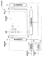
図13(A)〜(C)は、表示領域100Aを上下2つに分割し、分割した領域(表示領域100B,100C)ごとに、消光走査Sc1と発光走査Sc2を同時に行ったときの様子を表したものである。上側の表示領域100Bと下側の表示領域100Cとの継ぎ目(図13(C)の破線部分)が同時に発光するタイミングTxにおいて、異なるフレームの映像が表示される。このとき、映像が動画である場合には、上記の継ぎ目において、映像が不連続になってしまい、表示映像の品質が劣化してしまうという問題がある。
FIGS. 13A to 13C show a state in which the
本技術はかかる問題点に鑑みてなされたものであり、その目的は、高解像度化に伴う表示映像の品質劣化を低減することの可能な駆動回路ならびにそれを備えた表示装置および電子機器を提供することにある。 The present technology has been made in view of such problems, and an object of the present technology is to provide a drive circuit capable of reducing deterioration in quality of a display image accompanying an increase in resolution, and a display device and an electronic apparatus including the drive circuit. There is to do.
本技術の駆動回路は、第1表示領域および第2表示領域に対して、各画素の発光を行う第1垂直走査と、各画素の消光を行う第2垂直走査とを、1フレームにおいて第1表示領域および第2表示領域ごとに行う走査回路を備えている。第1表示領域および第2表示領域は、複数の画素が設けられた表示領域のうち、垂直方向に互いに隣接している。走査回路は、第2表示領域における、最先走査行のn+1フレーム目の発光開始のタイミングが、第1表示領域における、最終走査行のnフレーム目の発光終了のタイミングよりも遅くなるように、第1垂直走査および第2垂直走査を行う。上記の最先走査行は、第2表示領域において第1表示領域に隣接する画素行である。上記の最終走査行は、第1表示領域において第2表示領域に隣接する画素行である。上記のnは、正の整数をとる変数である。 The driving circuit according to the present technology performs, in one frame, a first vertical scan that performs light emission of each pixel and a second vertical scan that performs extinction of each pixel with respect to the first display region and the second display region. A scanning circuit is provided for each display area and second display area. The first display area and the second display area are adjacent to each other in the vertical direction among the display areas provided with a plurality of pixels. The scanning circuit is configured so that the light emission start timing of the (n + 1) th frame of the earliest scan row in the second display area is later than the light emission end timing of the nth frame of the last scan line in the first display area. A first vertical scan and a second vertical scan are performed. The earliest scanning row is a pixel row adjacent to the first display region in the second display region. The last scanning row is a pixel row adjacent to the second display region in the first display region. The above n is a variable that takes a positive integer.
本技術の表示装置は、複数の画素が設けられた表示領域を有する表示パネルと、各画素を駆動する駆動回路とを備えている。表示領域は、垂直方向に互いに隣接する第1表示領域および第2表示領域を含んでいる。駆動回路は、上記の駆動回路と同一の構成要素を有している。 The display device of the present technology includes a display panel having a display area provided with a plurality of pixels, and a drive circuit that drives each pixel. The display area includes a first display area and a second display area that are adjacent to each other in the vertical direction. The drive circuit has the same components as the drive circuit described above.
本技術の電子機器は、上記の表示装置を備えている。 An electronic apparatus of the present technology includes the display device described above.
本技術の駆動回路、表示装置および電子機器では、第2表示領域における、最先走査行のn+1フレーム目の発光開始のタイミングが、第1表示領域における、最終走査行のnフレーム目の発光終了のタイミングよりも遅くなっている。これにより、第2表示領域における、最先走査行のn+1フレーム目の発光期間と、第1表示領域における、最終走査行のnフレーム目の発光期間とが互いに重なり合うことがない。 In the driving circuit, the display device, and the electronic apparatus of the present technology, the light emission start timing of the (n + 1) th frame of the earliest scanning row in the second display region is the end of the light emission of the nth frame of the last scanning row in the first display region. It is later than the timing. As a result, the light emission period of the (n + 1) th frame of the earliest scan row in the second display area and the light emission period of the nth frame of the last scan line in the first display area do not overlap each other.
本技術の駆動回路、表示装置および電子機器によれば、第2表示領域における、最先走査行のn+1フレーム目の発光開始のタイミングが、第1表示領域における、最終走査行のnフレーム目の発光終了のタイミングよりも遅くなるようにしたので、継ぎ目における映像の不連続性に起因する表示映像の品質劣化を低減することができる。従って、高解像度化に伴う表示映像の品質劣化を低減することができる。 According to the driving circuit, the display device, and the electronic device of the present technology, the light emission start timing of the (n + 1) th frame of the earliest scanning row in the second display area is the nth frame of the last scanning line in the first display area. Since it is made later than the timing of the end of light emission, it is possible to reduce the quality deterioration of the display video due to the video discontinuity at the joint. Therefore, it is possible to reduce the deterioration of the quality of the displayed video accompanying the increase in resolution.
以下、発明を実施するための形態について、図面を参照して詳細に説明する。なお、説明は以下の順序で行う。
1.実施の形態(表示装置)
2.変形例(表示装置)
3.適用例(電子機器)
DESCRIPTION OF EMBODIMENTS Hereinafter, embodiments for carrying out the invention will be described in detail with reference to the drawings. The description will be given in the following order.
1. Embodiment (display device)
2. Modified example (display device)
3. Application example (electronic equipment)
<1.実施の形態>
[構成]
図1は、本技術の一実施の形態に係る表示装置1の概略構成を表したものである。この表示装置1は、表示パネル10と、外部から入力された映像信号20Aおよび同期信号20Bに基づいて表示パネル10を駆動する駆動回路20とを備えている。駆動回路20は、例えば、タイミング生成回路21、映像信号処理回路22、信号線駆動回路23、走査線駆動回路24、および電源線駆動回路25を有している。
<1. Embodiment>
[Constitution]
FIG. 1 illustrates a schematic configuration of a
(表示パネル10)
表示パネル10は、複数の画素11が表示パネル10の表示領域10A全面に渡ってマトリクス状に配置されたものである。表示パネル10は、駆動回路20によって各画素11がアクティブマトリクス駆動されることにより、外部から入力された映像信号20Aに基づく画像を表示するものである。
(Display panel 10)
The
図2は、画素11の回路構成の一例を表したものである。各画素11は、例えば、画素回路12と、有機EL素子13とを有している。有機EL素子13は、例えば、アノード電極、有機層およびカソード電極が順に積層された構成を有している。有機EL素子13は、素子容量Coled(図示せず)を有している。画素回路12は、有機EL素子13の発光・消光を制御するものである。画素回路12は、後述の書込走査S3によって各画素11に書き込んだ電圧を保持する機能を有している。画素回路12は、例えば、駆動トランジスタTr1、書込トランジスタTr2、保持容量Csおよび補助容量Csubによって構成されたものであり、2Tr2Cの回路構成となっている。
FIG. 2 illustrates an example of a circuit configuration of the
書込トランジスタTr2は、駆動トランジスタTr1のゲートに対する、映像信号に対応した信号電圧の印加を制御するものである。具体的には、書込トランジスタTr2は、後述の信号線DTLの電圧をサンプリングするとともに駆動トランジスタTr1のゲートに書き込むものである。駆動トランジスタTr1は、有機EL素子13を駆動するものであり、有機EL素子13に直列に接続されている。駆動トランジスタTr1は、書込トランジスタTr2によって書き込まれた電圧の大きさに応じて有機EL素子13に流れる電流を制御するものである。保持容量Csは、駆動トランジスタTr1のゲート−ソース間に所定の電圧を保持するものである。保持容量Csは、後述の待機期間中に駆動トランジスタTr1のゲート−ソース間電圧Vgsを一定に保持する役割を有する。補助容量Csubは、駆動トランジスタTr1から供給される電流の一部を流し込むものである。なお、画素回路12は、上述の2Tr2Cの回路に対して各種容量やトランジスタを付加した回路構成となっていてもよいし、上述の2Tr2Cの回路構成とは異なる回路構成となっていてもよい。
The write transistor Tr2 controls application of a signal voltage corresponding to the video signal to the gate of the drive transistor Tr1. Specifically, the write transistor Tr2 samples a voltage of a signal line DTL described later and writes it to the gate of the drive transistor Tr1. The drive transistor Tr1 drives the
駆動トランジスタTr1および書込トランジスタTr2は、例えば、nチャネルMOS型の薄膜トランジスタ(TFT(Thin Film Transistor))により形成されている。なお、TFTの種類は特に限定されるものではなく、例えば、逆スタガー構造(いわゆるボトムゲート型)であってもよいし、スタガー構造(トップゲート型)であってもよい。また、駆動トランジスタTr1および書込トランジスタTr2は、pチャネルMOS型のTFTにより形成されていてもよい。 The drive transistor Tr1 and the write transistor Tr2 are formed of, for example, an n-channel MOS thin film transistor (TFT (Thin Film Transistor)). Note that the type of TFT is not particularly limited, and may be, for example, an inverted staggered structure (so-called bottom gate type) or a staggered structure (top gate type). Further, the drive transistor Tr1 and the write transistor Tr2 may be formed of p-channel MOS type TFTs.
表示パネル10は、行方向に延在する複数の走査線WSLと、列方向に延在する複数の信号線DTLと、行方向に延在する複数の電源線DSLと、行方向に延在する複数のカソード線CTLを有している。なお、各カソード線CTLが共通の1枚のシート状の金属層で構成されていてもよい。走査線WSLは、各画素11の選択に用いられるものである。信号線DTLは、映像信号に応じた信号電圧の、各画素11への供給に用いられるものである。電源線DSLは、各画素11への駆動電流の供給に用いられるものである。
The
各信号線DTLと各走査線WSLとの交差点近傍には、画素11が設けられている。各信号線DTLは、後述の信号線駆動回路23の出力端(図示せず)と、書込トランジスタTr2のソースまたはドレインとに接続されている。各走査線WSLは、後述の走査線駆動回路24の出力端(図示せず)と、書込トランジスタTr2のゲートに接続されている。各電源線DSLは、固定の電圧を出力する電源の出力端(図示せず)と、駆動トランジスタTr1のソースまたはドレインに接続されている。カソード線CTLは、例えば、表示領域10Aの周囲に設けられた部材であって、かつ基準の電圧となっている部材に接続されている。
書込トランジスタTr2のゲートは、走査線WSLに接続されている。書込トランジスタTr2のソースまたはドレインが信号線DTLに接続されている。書込トランジスタTr2のソースおよびドレインのうち信号線DTLに未接続の端子が駆動トランジスタTr1のゲートに接続されている。駆動トランジスタTr1のソースまたはドレインが電源線DSLに接続されている。駆動トランジスタTr1のソースおよびドレインのうち電源線DSLに未接続の端子が有機EL素子13のアノードに接続されている。保持容量Csの一端が駆動トランジスタTr1のゲートに接続されている。保持容量Csの他端が駆動トランジスタTr1のソース(図2では有機EL素子13側の端子)に接続されている。つまり、保持容量Csは、駆動トランジスタTr1のゲート−ソース間に挿入されている。補助容量Csubの一端が駆動トランジスタTr1のソース(図2では有機EL素子13側の端子)に接続されている。補助容量Csubの他端がカソード線CTLに接続されている。
The gate of the writing transistor Tr2 is connected to the scanning line WSL. The source or drain of the write transistor Tr2 is connected to the signal line DTL. Of the source and drain of the write transistor Tr2, a terminal not connected to the signal line DTL is connected to the gate of the drive transistor Tr1. The source or drain of the drive transistor Tr1 is connected to the power supply line DSL. Of the source and drain of the drive transistor Tr1, a terminal not connected to the power supply line DSL is connected to the anode of the
(駆動回路20)
次に、駆動回路20について説明する。駆動回路20は、上述したように、例えば、タイミング生成回路21、映像信号処理回路22、信号線駆動回路23、走査線駆動回路24および電源線駆動回路25を有している。タイミング生成回路21は、駆動回路20内の各回路が連動して動作するように制御するものである。タイミング生成回路21は、例えば、外部から入力された同期信号20Bに応じて(同期して)、上述した各回路に対して制御信号21Aを出力するようになっている。
(Drive circuit 20)
Next, the
映像信号処理回路22は、例えば、外部から入力されたデジタルの映像信号20Aに対して所定の補正を行い、それにより得られた映像信号22Aを信号線駆動回路23に出力するものである。所定の補正としては、例えば、ガンマ補正や、オーバードライブ補正などが挙げられる。
For example, the video
信号線駆動回路23は、例えば、制御信号21Aの入力に応じて(同期して)、映像信号処理回路22から入力された映像信号22Aに対応するアナログの信号電圧を、各信号線DTLに印加するものである。信号線駆動回路23は、例えば、2種類の電圧(Vofs、Vsig)を出力可能となっている。具体的には、信号線駆動回路23は、走査線駆動回路24により選択された画素11へ、信号線DTLを介して2種類の電圧(Vofs、Vsig)を供給するようになっている。Vsigは、映像信号20Aに対応する電圧値となっている。Vofsは、映像信号20Aとは無関係の一定電圧である。Vsigの最小電圧はVofsよりも低い電圧値となっており、Vsigの最大電圧はVofsよりも高い電圧値となっている。
For example, the signal line drive circuit 23 applies an analog signal voltage corresponding to the
走査線駆動回路24は、例えば、制御信号21Aの入力に応じて(同期して)、複数の走査線WSLを所定のシーケンスで選択することにより、Vth補正や、信号電圧Vsigの書き込み、μ補正および待機を所望の順番で実行させるものである。ここで、Vth補正とは、駆動トランジスタTr1のゲート−ソース間電圧Vgsを駆動トランジスタTr1の閾値電圧に近づける補正動作を指している。信号電圧Vsigの書き込み(信号書き込み)とは、駆動トランジスタTr1のゲートに対して、信号電圧Vsigを、書込トランジスタTr2を介して書き込む動作を指している。μ補正とは、駆動トランジスタTr1のゲート−ソース間に保持される電圧(ゲート−ソース間電圧Vgs)を、駆動トランジスタTr1の移動度μの大きさに応じて補正する動作を指している。信号書き込みと、μ補正とは、互いに別個のタイミングで行われることもある。本実施の形態では、走査線駆動回路24が、1つの選択パルスを、走査線WSLへ出力することによって、信号書き込みと、μ補正とを同時に(もしくは間髪空けずに連続して)行うようになっている。待機とは、発光を開始できる状態で待機する(つまり消光状態を維持する)ことを指している。
For example, the scanning
走査線駆動回路24は、例えば、2種類の電圧(Von、Voff)を出力可能となっている。具体的には、走査線駆動回路24は、駆動対象の画素11へ、走査線WSLを介して2種類の電圧(Von、Voff)を供給し、書込トランジスタTr2のオンオフ制御を行うようになっている。ここで、Vonは、書込トランジスタTr2のオン電圧以上の値となっている。Vonは、後述の「Vth補正準備期間の後半部分」や、「Vth補正期間」、「信号書込・μ補正期間」などに走査線駆動回路24から出力される書込パルスの波高値である。Voffは、書込トランジスタTr2のオン電圧よりも低い値となっており、かつ、Vonよりも低い値となっている。Voffは、後述の「Vth補正準備期間の前半部分」や、「Vth補正休止期間」、「待機期間」、「発光期間」などに走査線駆動回路24から出力される書込パルスの波高値である。
For example, the scanning
電源線駆動回路25は、例えば、制御信号21Aの入力に応じて(同期して)、複数の電源線DSLを所定の単位ごとに順次選択するものである。電源線駆動回路25は、例えば、2種類の電圧(Vcc、Vss)を出力可能となっている。電源線駆動回路25は、走査線駆動回路24により選択された画素11へ、電源線DSLを介して2種類の電圧(Vcc、Vss)を供給するようになっている。ここで、Vssは、有機EL素子13の閾値電圧Velと、有機EL素子13のカソード電圧Vcathとを足し合わせた電圧(Vel+Vcath)よりも低い電圧値である。Vccは、電圧(Vel+Vcath)以上の電圧値である。
For example, the power supply
[動作]
次に、本実施の形態の表示装置1の動作(消光から発光までの動作)について説明する。本実施の形態では、有機EL素子13のI−V特性が経時変化しても、その影響を受けることなく、有機EL素子13の発光輝度を一定に保つようにするために、有機EL素子13のI−V特性の変動に対する補償動作を組み込んでいる。さらに、本実施の形態では、駆動トランジスタTr1の閾値電圧や移動度が経時変化しても、それらの影響を受けることなく、有機EL素子13の発光輝度を一定に保つようにするために、上記閾値電圧や上記移動度の変動に対する補正動作を組み込んでいる。
[Operation]
Next, the operation (operation from quenching to light emission) of the
図3は、1つの画素11に着目したときの走査線WSL、電源線DSLおよび信号線DTLに印加される電圧、ゲート電圧Vg、およびソース電圧Vsの経時変化の一例を表したものである。
FIG. 3 shows an example of changes over time of the voltage applied to the scanning line WSL, the power supply line DSL, and the signal line DTL, the gate voltage Vg, and the source voltage Vs when focusing on one
(Vth補正準備期間)
まず、駆動回路20は、駆動トランジスタTr1のゲート−ソース間電圧Vgsを駆動トランジスタTr1の閾値電圧に近づけるVth補正の準備を行う。具体的には、走査線WSLの電圧がVoff、信号線DTLの電圧がVofs、電源線DSLの電圧がVccとなっている時に、電源線駆動回路25は、制御信号21Aに応じて電源線DSLの電圧をVccからVssに下げる(時刻T1)。つまり、有機EL素子13が発光している時に、電源線駆動回路25は、制御信号21Aに応じて電源線DSLの電圧をVccからVssに下げる。すると、ソース電圧VsがVssまで下がり、有機EL素子13が消光する。このとき、保持容量Csを介したカップリングによりゲート電圧Vgも下がる。
(Vth correction preparation period)
First, the
次に、電源線DSLの電圧がVssとなっており、かつ信号線DTLの電圧がVofsとなっている間に、走査線駆動回路24は、制御信号21Aに応じて走査線WSLの電圧をVoffからVonに上げる(時刻T2)。すると、ゲート電圧VgがVofsまで下がる。このとき、ゲート電圧Vgとソース電圧Vsとの電位差(ゲート−ソース間電圧Vgs)が駆動トランジスタTr1の閾値電圧よりも小さくなっていてもよいし、それと等しいか、またはそれよりも大きくなっていてもよい。
Next, while the voltage of the power supply line DSL is Vss and the voltage of the signal line DTL is Vofs, the scanning
(Vth補正期間)
次に、駆動回路20は、Vthの補正を行う。具体的には、信号線DTLの電圧がVofsとなっており、かつ、走査線WSLの電圧がVonとなっている間に、電源線駆動回路25は、制御信号21Aに応じて電源線DSLの電圧をVssからVccに上げる(時刻T3)。すると、駆動トランジスタTr1のドレイン−ソース間に電流Idsが流れ、ソース電圧Vsが上昇する。このとき、ソース電圧VsがVofs−Vthよりも低い場合には、駆動トランジスタTr1がカットオフするまで、駆動トランジスタTr1のドレイン−ソース間に電流Idsが流れる。つまり、Vth補正がまだ完了していない場合には、ゲート−ソース間電圧VgsがVthになるまで、駆動トランジスタTr1のドレイン−ソース間に電流Idsが流れる。これにより、ゲート電圧VgがVofsとなり、ソース電圧Vsが上昇し、その結果、保持容量CsがVthに充電され、ゲート−ソース間電圧VgsがVthとなる。
(Vth correction period)
Next, the
その後、信号線駆動回路23は、制御信号21Aに応じて信号線DTLの電圧をVofsからVsigに切り替える前に、走査線駆動回路24が制御信号21Aに応じて走査線WSLの電圧をVonからVoffに下げる(時刻T4)。すると、駆動トランジスタTr1のゲートがフローティングとなるので、ゲート−ソース間電圧Vgsを信号線DTLの電圧の大きさに拘わらずVthのままで維持することができる。このように、ゲート−ソース間電圧VgsをVthに設定することにより、駆動トランジスタTr1の閾値電圧Vthが画素回路12ごとにばらついた場合であっても、有機EL素子13の発光輝度のばらつきをなくすことができる。
Thereafter, the signal line driving circuit 23 changes the voltage of the scanning line WSL from Von to Voff in accordance with the
(Vth補正休止期間)
その後、Vth補正の休止期間中に、信号線駆動回路23は、信号線DTLの電圧をVofsからVsigに切り替える。
(Vth correction suspension period)
Thereafter, during the suspension period of Vth correction, the signal line drive circuit 23 switches the voltage of the signal line DTL from Vofs to Vsig.
(信号書込・μ補正期間)
Vth補正休止期間が終了した後(つまりVth補正が完了した後)、駆動回路20は、映像信号20Aに応じた信号電圧の書き込みと、μ補正を行う。具体的には、信号線DTLの電圧がVsigとなっており、かつ電源線DSLの電圧がVccとなっている間に、走査線駆動回路24は、制御信号21Aに応じて走査線WSLの電圧をVoffからVonに上げる(時刻T5)。すると、駆動トランジスタTr1のゲートが信号線DTLに接続され、駆動トランジスタTr1のゲート電圧Vgが信号線DTLの電圧Vsigとなる。このとき、有機EL素子13のアノード電圧はこの段階ではまだ有機EL素子13の閾値電圧Velよりも小さく、有機EL素子13はカットオフしている。そのため、電流Idsは有機EL素子13の素子容量Coledおよび補助容量Csubに流れ、素子容量Coledおよび補助容量Csubが充電される。その結果、ソース電圧VsがΔVsだけ上昇し、やがてゲート−ソース間電圧VgsがVsig+Vth−ΔVsとなる。このようにして、書き込みと同時にμ補正が行われる。ここで、駆動トランジスタTr1の移動度μが大きい程、ΔVsも大きくなるので、ゲートソース間電圧Vgsを発光前にΔVだけ小さくすることにより、画素11ごとの移動度μのばらつきを取り除くことができる。
(Signal writing / μ correction period)
After the Vth correction pause period ends (that is, after the Vth correction is completed), the
(待機期間)
次に、駆動回路20は、待機を行う。具体的には、走査線駆動回路24が、制御信号21Aに応じて走査線WSLの電圧をVonからVoffに下げるとともに、電源線駆動回路25が、制御信号21Aに応じて電源線DSLの電圧をVccからVssに下げる(時刻T6)。なお、電源線DSLの電圧をVccからVssに下げる時が、走査線WSLの電圧をVonからVoffに下げる時と同時であってもよいし、走査線WSLの電圧をVonからVoffに下げる時よりも若干、遅れた時であってもよい。すると、駆動トランジスタTr1のゲートがフローティングとなるが、電源線DSLの電圧がVssに下がるので、有機EL素子13に閾値電圧Vel以上の電圧が印加されず、有機EL素子13は発光しない。このとき、ゲート−ソース間電圧Vgsは、Vsig+Vth−ΔVsとなったままである。
(Waiting period)
Next, the
(発光期間)
最後に、電源線駆動回路25が、制御信号21Aに応じて電源線DSLの電圧をVssからVccに上げる(時刻T7)。すると、駆動トランジスタTr1のドレイン−ソース間に電流Idsが流れ、ソース電圧Vsが上昇する。その結果、有機EL素子13に閾値電圧Vel以上の電圧が印加され、有機EL素子13が所望の輝度で発光する。
(Light emission period)
Finally, the power supply
図4は、表示領域10Aを上下2つに分割したときの、上側の表示領域(第1表示領域10B)と下側の表示領域(第2表示領域10C)での映像表示の一例を表したものである。図5は、第1表示領域10Bでの、WSL1〜WSL4,DSL1〜4、およびDTLに印加される電圧の経時変化の一例を表す波形図である。
FIG. 4 shows an example of video display in the upper display area (
本実施の形態では、表示領域10Aが、垂直方向に互いに隣接する第1表示領域10Bおよび第2表示領域10Cに分割されている。表示領域10Aは、M行の画素行を有している。第1表示領域10Bおよび第2表示領域10Cは、それぞれ、M/2行の画素行を有している。第1表示領域10Bでは、1行目の画素行が表示領域10Aの1行目の画素行となっている。さらに、第1表示領域10Bでは、最後の画素行(つまり、第2表示領域10Cに隣接する画素行)が表示領域10AのM/2画素行となっている。第2表示領域10Cでは、1行目の画素行(つまり、第1表示領域10Bに隣接する画素行)が表示領域10AのM/2+1画素行となっている。さらに、第2表示領域10Cでは、最後の画素行が表示領域10Aの最後の画素行(つまり、M画素行)となっている。
In the present embodiment, the
駆動回路20は、第1表示領域10Bを1画素行からM/2画素行に向かって垂直走査を行い、第2表示領域10CをM/2+1画素行からM画素行に向かって垂直走査を行う。駆動回路20は、第1表示領域10Bおよび第2表示領域10Cに対して、下記の(1)〜(5)の各種垂直走査を、1フレームにおいて第1表示領域10Bおよび第2表示領域10Cごとに行う。
(1)各画素11の消光を行う消光走査S1(第2垂直走査)
(2)Vth補正を行うVth補正走査S2
(3)映像信号に応じた電圧を各画素11に書き込むとともにμ補正を行う書込走査S3(第3垂直走査)
(4)書込走査Sc1に続いて各画素11の発光を待機させる待機走査S4(第4垂直走査)
(5)各画素11の発光を行う発光走査S5(第1垂直走査)
The
(1) Extinction scanning S1 (second vertical scanning) for extinguishing each
(2) Vth correction scanning S2 for performing Vth correction
(3) Write scan S3 (third vertical scan) for writing a voltage corresponding to the video signal to each
(4) Standby scan S4 (fourth vertical scan) for waiting for light emission of each
(5) Light emission scanning S5 for emitting light from each pixel 11 (first vertical scanning)
駆動回路20は、第2表示領域10Cにおける最先走査行(M/2+1画素行)のn+1フレーム目の発光開始のタイミングが、第1表示領域10Bにおける最終走査行(M/2画素行)のnフレーム目の発光終了のタイミングよりも遅くなるように、発光走査S5および消光走査S1を行う。上記のnは、正の整数をとる変数である。これにより、第2表示領域10Cにおける、最先走査行(M/2+1画素行)のn+1フレーム目の発光期間と、第1表示領域10Bにおける、最終走査行(M/2画素行)のnフレーム目の発光期間とが互いに重なり合うことがない。
In the
さらに、駆動回路20は、第1表示領域10Bの最終走査行のnフレーム目の発光期間と、第2表示領域10Cの最先走査行のnフレーム目の発光期間とが完全にまたは部分的に互いに重なり合うように、発光走査S5および消光走査S1を行う。第1表示領域10Bの最終走査行がM/2画素行であり、第2表示領域10Cの最先走査行がM/2+1画素行である。駆動回路20は、例えば、図4(A)、図4(B)に示したように、第1表示領域10Bおよび第2表示領域10Cに渡って連続して、発光走査S5および消光走査S1を行う。このようにした場合には、1フレームにおける表示領域10A中の発光領域が、1行目の画素行から最後の画素行に渡って連続かつ滑らかに遷移する。
Further, the driving
駆動回路20は、第1表示領域10Bおよび第2表示領域10Cにおいて、発光走査S5および消光走査S1の遷移速度を、Vth補正走査S2、書込走査S3および待機走査S4の遷移速度よりも早くする。言い換えると、駆動回路20は、第1表示領域10Bおよび第2表示領域10Cにおいて、Vth補正走査S2、書込走査S3および待機走査S4の遷移速度を、発光走査S5および消光走査S1の遷移速度よりも遅くする。駆動回路20は、第1表示領域10Bおよび第2表示領域10Cにおいて、発光走査S5および消光走査S1の遷移を、Vth補正走査S2、書込走査S3および待機走査S4の遷移速度の2倍の遷移速度で行う。言い換えると、駆動回路20は、第1表示領域10Bおよび第2表示領域10Cにおいて、Vth補正走査S2、書込走査S3および待機走査S4の遷移を、発光走査S5および消光走査S1の遷移速度の1/2倍の遷移速度で行う。駆動回路20は、例えば、図4(A)、図4(B)、図5(A)〜(I)に示したように、発光走査S5および消光走査S1を1/2H周期で行うとともに、Vth補正走査S2、書込走査S3および待機走査S4を1H周期で行う。このようにした場合、Vth補正走査S2、書込走査S3および待機走査S4の遷移速度が、表示領域10Aを分割せずに行うときの遷移速度の半分の遷移速度となる。
In the
このとき、待機期間は、図5(A)〜(I)に示したように、1画素行からM/2画素行に向かうにつれてΔt1、Δt2、Δt3、Δt4…と、短くなっている。同様に、待機期間は、M/2+1画素行からM画素行に向かうにつれて短くなっている。このように、待機時間を設定したり、画素行ごとに変えたりすることを可能にしているのは、駆動トランジスタTr1のゲート−ソース間電圧Vgsが待機期間中、保持容量Csによって一定に保たれているからである。 At this time, as shown in FIGS. 5A to 5I, the standby period becomes shorter as Δt1, Δt2, Δt3, Δt4,... As it goes from one pixel row to the M / 2 pixel row. Similarly, the standby period becomes shorter from the M / 2 + 1 pixel row toward the M pixel row. Thus, the standby time can be set or changed for each pixel row because the gate-source voltage Vgs of the drive transistor Tr1 is kept constant by the storage capacitor Cs during the standby period. Because.
駆動回路20が上述のような走査をした結果、例えば、図4(A)、図4(B)に記載の時刻Txでの映像が、図4(C)のようになる。具体的には、時刻Txでは、第1表示領域10Bの最終走査行にはnフレーム目の映像が表示されており、第2表示領域10Cの最先走査行にはnフレーム目の映像が表示されている。表示領域10Aが第1表示領域10Bおよび第2表示領域10Cによって分割された境界(分割ラインL)で、第1表示領域10Bに表示されたnフレーム目の映像と、第2表示領域10Cに表示されたnフレーム目の映像とが連続して表示されている。
As a result of the scanning performed by the
[効果]
次に、本実施の形態の表示装置1における効果について説明する。
[effect]
Next, the effect in the
図13(A)〜(C)は、比較例にかかる表示装置の表示領域100Aを上下2つに分割したときの、上側の表示領域(表示領域100B)と下側の表示領域(表示領域100C)での映像表示の一例を表したものである。上側の表示領域100Bと下側の表示領域100Cとの継ぎ目(図13(C)の破線部分)が同時に発光するタイミングTxにおいて、異なるフレームの映像が表示される。このとき、映像が動画である場合には、上記の継ぎ目において、映像が不連続になってしまい、表示映像の品質が劣化してしまう。
13A to 13C show an upper display area (
一方、本実施の形態では、第2表示領域10Cにおける、最先走査行のn+1フレーム目の発光開始のタイミングが、第1表示領域10Bにおける、最終走査行のnフレーム目の発光終了のタイミングよりも遅くなっている。これにより、分割ラインLにおける映像の不連続性に起因する表示映像の品質劣化を低減することができる。従って、高解像度化に伴う表示映像の品質劣化を低減することができる。
On the other hand, in the present embodiment, the light emission start timing of the (n + 1) th frame of the earliest scanning row in the second display area 10C is higher than the light emission end timing of the nth frame of the last scanning row in the
また、本実施の形態では、第1表示領域10Bおよび第2表示領域10Cにおいて、Vth補正走査S2、書込走査S3および待機走査S4の遷移速度を、発光走査S5および消光走査S1の遷移速度よりも遅くすることができる。これにより、高精細化や、大画面化に伴って、1Hが短くなった場合であっても、Vth補正時間を確保することができる。
Further, in the present embodiment, in the
<2.変形例>
以下に、上記実施の形態の表示装置1の種々の変形例について説明する。なお、以下では、上記実施の形態の表示装置1と共通する構成要素に対しては、同一の符号が付与される。さらに、上記実施の形態の表示装置1と共通する構成要素についての説明は、適宜、省略されるものとする。
<2. Modification>
Below, the various modifications of the
[変形例1]
図6は、表示領域10Aを上下2つに分割したときの、上側の表示領域(第1表示領域10B)と下側の表示領域(第2表示領域10C)での映像表示の一変形例を表したものである。本変形例では、駆動回路20は、第1表示領域10Bおよび第2表示領域10Cにおいて、Vth補正走査S2、書込走査S3および待機走査S4の遷移を、発光走査S5および消光走査S1の遷移速度と同じ遷移速度で行う。Vth補正時間を確保することができるのであれば、このような駆動方法を採ることも可能である。
[Modification 1]
FIG. 6 shows a modified example of video display in the upper display area (
[変形例2]
上記実施の形態において、駆動トランジスタTr1と、電源線DSLとの間に、スイッチングトランジスタTr3が挿入されていてもよい(図7参照)。スイッチングトランジスタTr3のゲートには、スイッチング線SWLが接続されている。
[Modification 2]
In the above embodiment, the switching transistor Tr3 may be inserted between the drive transistor Tr1 and the power supply line DSL (see FIG. 7). A switching line SWL is connected to the gate of the switching transistor Tr3.
本変形例では、走査線駆動回路24が、スイッチング線SWLを介して、スイッチングトランジスタTr3をオン、オフ制御するようになっている。電源線駆動回路25は、例えば、各電源線DSLに対して所定の電圧を印加するものであり、例えば、Vccを出力可能となっている。上記実施の形態において電源線DSLにVssが印加される期間に、走査線駆動回路24は、スイッチング線SWLをオンするようになっている。
In this modification, the scanning
[変形例3]
上記実施の形態および変形例1,2では、表示領域10Aが2つの領域(第1表示領域10B,第2表示領域10C)に分割されていたが、3つ以上の領域に分割されていてもよい。この場合、駆動回路20が、垂直方向に互いに隣接する2つの領域に対して、上記実施の形態および変形例1,2に記載の方法で垂直走査を行えばよい。
[Modification 3]
Although the
[変形例4]
上記実施の形態および変形例1〜3において、有機EL素子13の代わりに、無機EL素子、LED、または半導体レーザなどが設けられていてもよい。
[Modification 4]
In the said embodiment and the modifications 1-3, the inorganic EL element, LED, or semiconductor laser etc. may be provided instead of the
<3.適用例>
以下、上記実施の形態およびその変形例(以下、「上記実施の形態等」と称する。)で説明した表示装置1の適用例について説明する。上記実施の形態の表示装置1は、テレビジョン装置、デジタルカメラ、ノート型パーソナルコンピュータ、携帯電話等の携帯端末装置あるいはビデオカメラなど、外部から入力された映像信号あるいは内部で生成した映像信号を、画像あるいは映像として表示するあらゆる分野の電子機器の表示装置に適用することが可能である。
<3. Application example>
Hereinafter, application examples of the
(適用例1)
図8は、上記実施の形態等の表示装置1が適用されるテレビジョン装置の外観を表したものである。このテレビジョン装置は、例えば、フロントパネル310およびフィルターガラス320を含む映像表示画面部300を有しており、この映像表示画面部300は、上記実施の形態およびその変形例に係る表示装置1により構成されている。
(Application example 1)
FIG. 8 illustrates an appearance of a television device to which the
(適用例2)
図9は、上記実施の形態等の表示装置1が適用されるデジタルカメラの外観を表したものである。このデジタルカメラは、例えば、フラッシュ用の発光部410、表示部420、メニュースイッチ430およびシャッターボタン440を有しており、その表示部420は、上記実施の形態等に係る表示装置1により構成されている。
(Application example 2)
FIG. 9 illustrates an appearance of a digital camera to which the
(適用例3)
図10は、上記実施の形態等の表示装置1が適用されるノート型パーソナルコンピュータの外観を表したものである。このノート型パーソナルコンピュータは、例えば、本体510,文字等の入力操作のためのキーボード520および画像を表示する表示部530を有しており、その表示部530は、上記実施の形態等に係る表示装置1により構成されている。
(Application example 3)
FIG. 10 illustrates an appearance of a notebook personal computer to which the
(適用例4)
図11は、上記実施の形態等の表示装置1が適用されるビデオカメラの外観を表したものである。このビデオカメラは、例えば、本体部610,この本体部610の前方側面に設けられた被写体撮影用のレンズ620,撮影時のスタート/ストップスイッチ630および表示部640を有しており、その表示部640は、上記実施の形態等に係る表示装置1により構成されている。
(Application example 4)
FIG. 11 illustrates an appearance of a video camera to which the
(適用例5)
図12は、上記実施の形態等の表示装置1が適用される携帯電話機の外観を表したものである。この携帯電話機は、例えば、上側筐体710と下側筐体720とを連結部(ヒンジ部)730で連結したものであり、ディスプレイ740,サブディスプレイ750,ピクチャーライト760およびカメラ770を有している。そのディスプレイ740またはサブディスプレイ750は、上記実施の形態等に係る表示装置1により構成されている。
(Application example 5)
FIG. 12 illustrates an appearance of a mobile phone to which the
以上、実施の形態および適用例を挙げて本技術を説明したが、本技術は上記実施の形態等に限定されるものではなく、種々変形が可能である。 While the present technology has been described with the embodiment and application examples, the present technology is not limited to the above-described embodiment and the like, and various modifications are possible.
例えば、上記実施の形態等では、アクティブマトリクス駆動のための画素回路12の構成は、上記各実施の形態で説明したものに限られず、必要に応じて容量素子やトランジスタを追加してもよい。その場合、画素回路12の変更に応じて、上述した信号線駆動回路23や、走査線駆動回路24、電源線駆動回路25などの他に、必要な駆動回路を追加してもよい。
For example, in the above embodiment and the like, the configuration of the
また、上記実施の形態等では、信号線駆動回路23、走査線駆動回路24および電源線駆動回路25の駆動をタイミング生成回路21および映像信号処理回路22が制御していたが、他の回路がこれらの駆動を制御するようにしてもよい。また、信号線駆動回路23、走査線駆動回路24および電源線駆動回路25の制御は、ハードウェア(回路)で行われていてもよいし、ソフトウェア(プログラム)で行われていてもよい。
In the above-described embodiment, the
また、上記実施の形態等では、書込トランジスタTr2のソースおよびドレインや、駆動トランジスタTr1のソースおよびドレインが固定されたものとして説明されていたが、いうまでもなく、電流の流れる向きによっては、ソースとドレインの対向関係が上記の説明とは逆になることがある。そのときは、上記実施の形態等において、ソースをドレインと読み替えるとともに、ドレインをソースと読み替えてもよい。 In the above-described embodiment and the like, the source and drain of the writing transistor Tr2 and the source and drain of the driving transistor Tr1 are described as being fixed. Needless to say, depending on the direction of current flow, The opposing relationship between the source and the drain may be opposite to the above description. In that case, in the above embodiment and the like, the source may be read as the drain and the drain may be read as the source.
また、上記実施の形態等では、書込トランジスタTr2および駆動トランジスタTr1がnチャネルMOS型のTFTにより形成されているものとして説明されていたが、書込トランジスタTr2および駆動トランジスタTr1の少なくとも一方がpチャネルMOS型のTFTにより形成されていてもよい。なお、駆動トランジスタTr1がpチャネルMOS型のTFTにより形成されている場合には、上記実施の形態等において、有機EL素子13のアノードがカソードとなり、有機EL素子13のカソードがアノードとなる。また、上記実施の形態等において、書込トランジスタTr2および駆動トランジスタTr1は、常に、アモルファスシリコン型のTFTやマイクロシリコン型のTFTである必要はなく、例えば、低温ポリシリコン型のTFTや、酸化物半導体TFTであってもよい。
In the above-described embodiments and the like, it has been described that the write transistor Tr2 and the drive transistor Tr1 are formed by n-channel MOS type TFTs. However, at least one of the write transistor Tr2 and the drive transistor Tr1 is p It may be formed by a channel MOS type TFT. When the drive transistor Tr1 is formed of a p-channel MOS type TFT, the anode of the
また、例えば、本技術は以下のような構成を取ることができる。
(1)
複数の画素が設けられた表示領域のうち、垂直方向に互いに隣接する第1表示領域および第2表示領域に対して、各前記画素の発光を行う第1垂直走査と、各前記画素の消光を行う第2垂直走査とを、1フレームにおいて前記第1表示領域および前記第2表示領域ごとに行う走査回路を備え、
前記走査回路は、前記第2表示領域における、前記第1表示領域に隣接する最先走査行のn+1フレーム目の発光開始のタイミングが、前記第1表示領域における、前記第2表示領域に隣接する最終走査行のnフレーム目の発光終了のタイミングよりも遅くなるように、前記第1垂直走査および前記第2垂直走査を行う
駆動回路。
(2)
前記走査回路は、前記最終走査行のnフレーム目の発光期間と、前記最先走査行のnフレーム目の発光期間とが完全にまたは部分的に互いに重なり合うように、前記第1垂直走査および前記第2垂直走査を行う
(1)に記載の駆動回路。
(3)
前記走査回路は、前記第1表示領域および前記第2表示領域に対して、映像信号に応じた電圧を各前記画素に書き込む第3垂直走査と、前記第3垂直走査に続いて各前記画素の発光を待機させる第4垂直走査とを、前記第2垂直走査による消光後であって、かつ前記第1垂直走査による発光前の期間に、1フレームにおいて前記第1表示領域および前記第2表示領域ごとに行う
(1)または(2)に記載の駆動回路。
(4)
前記走査回路は、前記第1垂直走査および前記第2垂直走査の遷移速度を、前記第3垂直走査および前記第4垂直走査の遷移速度よりも早くする
(3)に記載の駆動回路。
(5)
前記表示領域は、前記第1表示領域および前記第2表示領域からなり、
前記走査回路は、前記第1垂直走査および前記第2垂直走査を、前記第3垂直走査および前記第4垂直走査の遷移速度の2倍の遷移速度で行う
(4)に記載の駆動回路。
(6)
複数の画素が設けられた表示領域を有する表示パネルと、
各前記画素を駆動する駆動回路と
を備え、
前記表示領域は、垂直方向に互いに隣接する第1表示領域および第2表示領域を含み、
前記駆動回路は、前記第1表示領域および前記第2表示領域に対して、各前記画素の発光を行う第1垂直走査と、各前記画素の消光を行う第2垂直走査とを、1フレームにおいて前記第1表示領域および前記第2表示領域ごとに行う走査回路を有し、
前記走査回路は、前記第2表示領域における、前記第1表示領域に隣接する最先走査行のn+1フレーム目の発光開始のタイミングが、前記第1表示領域における、前記第2表示領域に隣接する最終走査行のnフレーム目の発光終了のタイミングよりも遅くなるように、前記第1垂直走査および前記第2垂直走査を行う
表示装置。
(7)
前記走査回路は、前記第1表示領域および前記第2表示領域に対して、映像信号に応じた電圧を各前記画素に書き込む第3垂直走査と、前記第3垂直走査に続いて各前記画素の発光を待機させる第4垂直走査とを、前記第2垂直走査による消光後であって、かつ前記第1垂直走査による発光前の期間に、1フレームにおいて前記第1表示領域および前記第2表示領域ごとに行う
(6)に記載の表示装置。
(8)
各前記画素は、発光素子と、前記第3垂直走査によって各前記画素に書き込んだ電圧を保持する画素回路とを有する
(7)に記載の表示装置。
(9)
表示装置を備え、
前記表示装置は、
複数の画素が設けられた表示領域を有する表示パネルと、
各前記画素を駆動する駆動回路と
を有し、
前記表示領域は、垂直方向に互いに隣接する第1表示領域および第2表示領域を含み、
前記駆動回路は、前記第1表示領域および前記第2表示領域に対して、各前記画素の発光を行う第1垂直走査と、各前記画素の消光を行う第2垂直走査とを、1フレームにおいて前記第1表示領域および前記第2表示領域ごとに行う走査回路を有し、
前記走査回路は、前記第2表示領域における、前記第1表示領域に隣接する最先走査行のn+1フレーム目の発光開始のタイミングが、前記第1表示領域における、前記第2表示領域に隣接する最終走査行のnフレーム目の発光終了のタイミングよりも遅くなるように、前記第1垂直走査および前記第2垂直走査を行う
電子機器。
For example, this technique can take the following composition.
(1)
Among the display areas provided with a plurality of pixels, a first vertical scan that emits light from each pixel and a quenching of each pixel are performed on a first display area and a second display area that are adjacent to each other in the vertical direction. A scanning circuit that performs the second vertical scanning to be performed for each of the first display area and the second display area in one frame;
In the scanning circuit, the light emission start timing of the (n + 1) th frame of the earliest scanning row adjacent to the first display area in the second display area is adjacent to the second display area in the first display area. A drive circuit that performs the first vertical scan and the second vertical scan so as to be later than the light emission end timing of the nth frame of the last scan row.
(2)
The scanning circuit includes the first vertical scan and the light emission period of the nth frame of the last scan row and the light emission period of the nth frame of the earliest scan row so that the light emission period overlaps each other completely or partially. The drive circuit according to (1), wherein the second vertical scanning is performed.
(3)
The scanning circuit is configured to write a voltage corresponding to a video signal to each pixel with respect to the first display area and the second display area, and each of the pixels following the third vertical scan. The fourth vertical scanning for waiting for light emission is the period after the extinction by the second vertical scanning and before the light emission by the first vertical scanning, in the first display area and the second display area in one frame. The driving circuit according to (1) or (2).
(4)
The drive circuit according to (3), wherein the scanning circuit makes a transition speed of the first vertical scan and the second vertical scan faster than a transition speed of the third vertical scan and the fourth vertical scan.
(5)
The display area includes the first display area and the second display area,
The drive circuit according to (4), wherein the scanning circuit performs the first vertical scanning and the second vertical scanning at a transition speed that is twice the transition speed of the third vertical scanning and the fourth vertical scanning.
(6)
A display panel having a display area provided with a plurality of pixels;
A drive circuit for driving each of the pixels,
The display area includes a first display area and a second display area that are adjacent to each other in the vertical direction,
The drive circuit performs, in one frame, a first vertical scan that emits light from the pixels and a second vertical scan that extinguishes the pixels with respect to the first display area and the second display area. A scanning circuit for each of the first display area and the second display area;
In the scanning circuit, the light emission start timing of the (n + 1) th frame of the earliest scanning row adjacent to the first display area in the second display area is adjacent to the second display area in the first display area. A display device that performs the first vertical scanning and the second vertical scanning so as to be later than the timing of the end of light emission of the nth frame of the last scanning row.
(7)
The scanning circuit is configured to write a voltage corresponding to a video signal to each pixel with respect to the first display area and the second display area, and each of the pixels following the third vertical scan. The fourth vertical scanning for waiting for light emission is the period after the extinction by the second vertical scanning and before the light emission by the first vertical scanning, in the first display area and the second display area in one frame. (6) The display device according to (6).
(8)
Each said pixel has a light emitting element and the pixel circuit holding the voltage written in each said pixel by the said 3rd vertical scanning. (7).
(9)
A display device,
The display device
A display panel having a display area provided with a plurality of pixels;
A drive circuit for driving each of the pixels,
The display area includes a first display area and a second display area that are adjacent to each other in the vertical direction,
The drive circuit performs, in one frame, a first vertical scan that emits light from the pixels and a second vertical scan that extinguishes the pixels with respect to the first display area and the second display area. A scanning circuit for each of the first display area and the second display area;
In the scanning circuit, the light emission start timing of the (n + 1) th frame of the earliest scanning row adjacent to the first display area in the second display area is adjacent to the second display area in the first display area. An electronic device that performs the first vertical scanning and the second vertical scanning so as to be later than the light emission end timing of the nth frame of the last scanning row.
1…表示装置、10…表示パネル、10A…表示領域、10B…第1表示領域、10C…第2表示領域、11…画素、12…画素回路、13…有機EL素子、14…LED、20…駆動回路、20A…映像信号、20B…同期信号、21…タイミング生成回路、21A…制御信号、22…映像信号処理回路、22A…映像信号、23…信号線駆動回路、24…走査線駆動回路、25…電源線駆動回路、300…映像表示画面部、310…フロントパネル、320…フィルターガラス、410…発光部、420,530,640…表示部、430…メニュースイッチ、440…シャッターボタン、510…本体、520…キーボード、610…本体部、620…レンズ、630…スタート/ストップスイッチ、710…上側筐体、720…下側筐体、730…連結部、740…ディスプレイ、750…サブディスプレイ、760…ピクチャーライト、770…カメラ、Cs…保持容量、CTL…グラウンド線、DTL…信号線、DSL,DSL1,DSL2,DSL3,DSL4…電源線、Ids…電流、S1…消光走査、S2…閾値補正走査、S3…書き込み走査、S4…待機走査、S5…発光走査、Sa1,Sa2…消光走査、Sb1,Sb2…閾値補正走査、Sc1,Sc2…書き込み走査、Sd1,Sd2…待機走査、Se1,Se2…発光走査、T1,T2,T3,T4,T5,T6,T7,Tx…時刻、Tr1…駆動トランジスタ、Tr2…書込トランジスタ、Tr3…スイッチングトランジスタ、Vcc,Vofs,Voff,Von,Vsig,Vss…電圧、Vg…ゲート電圧、Vgs…ゲート−ソース間電圧、Voled…有機EL素子の電圧、Vs…ソース電圧、Vth…閾値電圧、WSL,WSL1,WSL2,WSL3,WSL4…走査線、Δt…差分、Δt1,Δt2,Δt3,Δt4…待機時間。
DESCRIPTION OF
Claims (9)
前記走査回路は、前記第2表示領域における、前記第1表示領域に隣接する最先走査行のn+1フレーム目の発光開始のタイミングが、前記第1表示領域における、前記第2表示領域に隣接する最終走査行のnフレーム目の発光終了のタイミングよりも遅くなるように、前記第1垂直走査および前記第2垂直走査を行う
駆動回路。 Among the display areas provided with a plurality of pixels, a first vertical scan that emits light from each pixel and a quenching of each pixel are performed on a first display area and a second display area that are adjacent to each other in the vertical direction. A scanning circuit that performs the second vertical scanning to be performed for each of the first display area and the second display area in one frame;
In the scanning circuit, the light emission start timing of the (n + 1) th frame of the earliest scanning row adjacent to the first display area in the second display area is adjacent to the second display area in the first display area. A drive circuit that performs the first vertical scan and the second vertical scan so as to be later than the light emission end timing of the nth frame of the last scan row.
請求項1に記載の駆動回路。 The scanning circuit includes the first vertical scan and the light emission period of the nth frame of the last scan row and the light emission period of the nth frame of the earliest scan row so that the light emission period overlaps each other completely or partially. The driving circuit according to claim 1, wherein the second vertical scanning is performed.
請求項2に記載の駆動回路。 The scanning circuit is configured to write a voltage corresponding to a video signal to each pixel with respect to the first display area and the second display area, and each of the pixels following the third vertical scan. The fourth vertical scanning for waiting for light emission is the period after the extinction by the second vertical scanning and before the light emission by the first vertical scanning, in the first display area and the second display area in one frame. The driving circuit according to claim 2, which is performed every time.
請求項3に記載の駆動回路。 The drive circuit according to claim 3, wherein the scanning circuit makes a transition speed of the first vertical scanning and the second vertical scanning faster than a transition speed of the third vertical scanning and the fourth vertical scanning.
前記走査回路は、前記第1垂直走査および前記第2垂直走査を、前記第3垂直走査および前記第4垂直走査の遷移速度の2倍の遷移速度で行う
請求項4に記載の駆動回路。 The display area includes the first display area and the second display area,
5. The drive circuit according to claim 4, wherein the scanning circuit performs the first vertical scanning and the second vertical scanning at a transition speed that is twice the transition speed of the third vertical scanning and the fourth vertical scanning.
各前記画素を駆動する駆動回路と
を備え、
前記表示領域は、垂直方向に互いに隣接する第1表示領域および第2表示領域を含み、
前記駆動回路は、前記第1表示領域および前記第2表示領域に対して、各前記画素の発光を行う第1垂直走査と、各前記画素の消光を行う第2垂直走査とを、1フレームにおいて前記第1表示領域および前記第2表示領域ごとに行う走査回路を有し、
前記走査回路は、前記第2表示領域における、前記第1表示領域に隣接する最先走査行のn+1フレーム目の発光開始のタイミングが、前記第1表示領域における、前記第2表示領域に隣接する最終走査行のnフレーム目の発光終了のタイミングよりも遅くなるように、前記第1垂直走査および前記第2垂直走査を行う
表示装置。 A display panel having a display area provided with a plurality of pixels;
A drive circuit for driving each of the pixels,
The display area includes a first display area and a second display area that are adjacent to each other in the vertical direction,
The drive circuit performs, in one frame, a first vertical scan that emits light from the pixels and a second vertical scan that extinguishes the pixels with respect to the first display area and the second display area. A scanning circuit for each of the first display area and the second display area;
In the scanning circuit, the light emission start timing of the (n + 1) th frame of the earliest scanning row adjacent to the first display area in the second display area is adjacent to the second display area in the first display area. A display device that performs the first vertical scanning and the second vertical scanning so as to be later than the timing of the end of light emission of the nth frame of the last scanning row.
請求項6に記載の表示装置。 The scanning circuit is configured to write a voltage corresponding to a video signal to each pixel with respect to the first display area and the second display area, and each of the pixels following the third vertical scan. The fourth vertical scanning for waiting for light emission is the period after the extinction by the second vertical scanning and before the light emission by the first vertical scanning, in the first display area and the second display area in one frame. The display device according to claim 6, which is performed every time.
請求項7に記載の表示装置。 The display device according to claim 7, wherein each of the pixels includes a light emitting element and a pixel circuit that holds a voltage written in the pixel by the third vertical scanning.
前記表示装置は、
複数の画素が設けられた表示領域を有する表示パネルと、
各前記画素を駆動する駆動回路と
を有し、
前記表示領域は、垂直方向に互いに隣接する第1表示領域および第2表示領域を含み、
前記駆動回路は、前記第1表示領域および前記第2表示領域に対して、各前記画素の発光を行う第1垂直走査と、各前記画素の消光を行う第2垂直走査とを、1フレームにおいて前記第1表示領域および前記第2表示領域ごとに行う走査回路を有し、
前記走査回路は、前記第2表示領域における、前記第1表示領域に隣接する最先走査行のn+1フレーム目の発光開始のタイミングが、前記第1表示領域における、前記第2表示領域に隣接する最終走査行のnフレーム目の発光終了のタイミングよりも遅くなるように、前記第1垂直走査および前記第2垂直走査を行う
電子機器。 A display device,
The display device
A display panel having a display area provided with a plurality of pixels;
A drive circuit for driving each of the pixels,
The display area includes a first display area and a second display area that are adjacent to each other in the vertical direction,
The drive circuit performs, in one frame, a first vertical scan that emits light from the pixels and a second vertical scan that extinguishes the pixels with respect to the first display area and the second display area. A scanning circuit for each of the first display area and the second display area;
In the scanning circuit, the light emission start timing of the (n + 1) th frame of the earliest scanning row adjacent to the first display area in the second display area is adjacent to the second display area in the first display area. An electronic device that performs the first vertical scanning and the second vertical scanning so as to be later than the light emission end timing of the nth frame of the last scanning row.
Priority Applications (2)
| Application Number | Priority Date | Filing Date | Title |
|---|---|---|---|
| JP2013247230A JP2015106003A (en) | 2013-11-29 | 2013-11-29 | Drive circuit, display device, and electronic apparatus |
| US14/539,218 US9852684B2 (en) | 2013-11-29 | 2014-11-12 | Drive circuit, display unit, and electronic apparatus |
Applications Claiming Priority (1)
| Application Number | Priority Date | Filing Date | Title |
|---|---|---|---|
| JP2013247230A JP2015106003A (en) | 2013-11-29 | 2013-11-29 | Drive circuit, display device, and electronic apparatus |
Publications (2)
| Publication Number | Publication Date |
|---|---|
| JP2015106003A true JP2015106003A (en) | 2015-06-08 |
| JP2015106003A5 JP2015106003A5 (en) | 2016-09-23 |
Family
ID=53265812
Family Applications (1)
| Application Number | Title | Priority Date | Filing Date |
|---|---|---|---|
| JP2013247230A Pending JP2015106003A (en) | 2013-11-29 | 2013-11-29 | Drive circuit, display device, and electronic apparatus |
Country Status (2)
| Country | Link |
|---|---|
| US (1) | US9852684B2 (en) |
| JP (1) | JP2015106003A (en) |
Cited By (1)
| Publication number | Priority date | Publication date | Assignee | Title |
|---|---|---|---|---|
| CN114974133A (en) * | 2022-06-27 | 2022-08-30 | 武汉天马微电子有限公司 | Display panel and display device |
Families Citing this family (1)
| Publication number | Priority date | Publication date | Assignee | Title |
|---|---|---|---|---|
| JP6201465B2 (en) | 2013-07-08 | 2017-09-27 | ソニー株式会社 | Display device, driving method of display device, and electronic apparatus |
Citations (2)
| Publication number | Priority date | Publication date | Assignee | Title |
|---|---|---|---|---|
| JP2011133652A (en) * | 2009-12-24 | 2011-07-07 | Sony Corp | Display panel module, semiconductor integrated circuit, driving method of pixel array unit, and electronic apparatus |
| WO2013088483A1 (en) * | 2011-12-16 | 2013-06-20 | パナソニック株式会社 | Display device and method for driving same |
Family Cites Families (4)
| Publication number | Priority date | Publication date | Assignee | Title |
|---|---|---|---|---|
| JP5012729B2 (en) * | 2008-08-08 | 2012-08-29 | ソニー株式会社 | Display panel module, semiconductor integrated circuit, pixel array driving method, and electronic apparatus |
| JP5012728B2 (en) * | 2008-08-08 | 2012-08-29 | ソニー株式会社 | Display panel module, semiconductor integrated circuit, pixel array driving method, and electronic apparatus |
| JP5380996B2 (en) * | 2008-10-10 | 2014-01-08 | ソニー株式会社 | Three-dimensional image system, display device, shutter operation synchronization device of three-dimensional image system, shutter operation synchronization method of three-dimensional image system, and electronic device |
| JP2013114112A (en) | 2011-11-30 | 2013-06-10 | Sony Corp | Resolution converting device and method |
-
2013
- 2013-11-29 JP JP2013247230A patent/JP2015106003A/en active Pending
-
2014
- 2014-11-12 US US14/539,218 patent/US9852684B2/en active Active
Patent Citations (2)
| Publication number | Priority date | Publication date | Assignee | Title |
|---|---|---|---|---|
| JP2011133652A (en) * | 2009-12-24 | 2011-07-07 | Sony Corp | Display panel module, semiconductor integrated circuit, driving method of pixel array unit, and electronic apparatus |
| WO2013088483A1 (en) * | 2011-12-16 | 2013-06-20 | パナソニック株式会社 | Display device and method for driving same |
Cited By (1)
| Publication number | Priority date | Publication date | Assignee | Title |
|---|---|---|---|---|
| CN114974133A (en) * | 2022-06-27 | 2022-08-30 | 武汉天马微电子有限公司 | Display panel and display device |
Also Published As
| Publication number | Publication date |
|---|---|
| US20150154911A1 (en) | 2015-06-04 |
| US9852684B2 (en) | 2017-12-26 |
Similar Documents
| Publication | Publication Date | Title |
|---|---|---|
| JP6159965B2 (en) | Display panel, display device and electronic device | |
| JP6853662B2 (en) | Display panel and display device | |
| JP2012185328A (en) | Pixel circuit, display panel, display device, and electronic appliance | |
| JP2009288749A (en) | Display device, its drive method and electronic apparatus | |
| JP4433039B2 (en) | Display device, driving method thereof, and electronic apparatus | |
| JP2011175103A (en) | Pixel circuit, display device and method for driving the same, and electronic equipment | |
| JP6736276B2 (en) | Display panel and display device | |
| WO2013061767A1 (en) | Drive circuit, drive method, display device, and electronic device | |
| JP2009080365A (en) | Display device, its driving method, and electronic equipment | |
| JP2015094773A (en) | Display device and electronic apparatus | |
| JP2009080367A (en) | Display device, its driving method, and electronic equipment | |
| KR101992491B1 (en) | Pixel circuit, display panel, display unit, and electronic system | |
| JP2009080366A (en) | Display device, its driving method, and electronic equipment | |
| WO2014112278A1 (en) | Display device, display drive device, drive method, and electronic apparatus | |
| JP2015106003A (en) | Drive circuit, display device, and electronic apparatus | |
| JP5891493B2 (en) | Display panel, driving method thereof, display device, and electronic apparatus | |
| JP2011221165A (en) | Display device, electronic device, and driving method of display device | |
| KR102618390B1 (en) | Display device and driving method thereof | |
| US9378677B2 (en) | Drive circuit, display unit, and electronic apparatus | |
| JP6781176B2 (en) | Pixel circuit and display device | |
| JP6789796B2 (en) | Display device and drive method | |
| JP6732822B2 (en) | Pixel circuit and display device | |
| JP6774325B2 (en) | Pixel circuit and display device | |
| JP2009098429A (en) | Display device and electronic apparatus | |
| JP2015090478A (en) | Display device and electronic apparatus |
Legal Events
| Date | Code | Title | Description |
|---|---|---|---|
| A711 | Notification of change in applicant |
Free format text: JAPANESE INTERMEDIATE CODE: A712 Effective date: 20150327 |
|
| A521 | Request for written amendment filed |
Free format text: JAPANESE INTERMEDIATE CODE: A523 Effective date: 20160808 |
|
| A621 | Written request for application examination |
Free format text: JAPANESE INTERMEDIATE CODE: A621 Effective date: 20160808 |
|
| A977 | Report on retrieval |
Free format text: JAPANESE INTERMEDIATE CODE: A971007 Effective date: 20170518 |
|
| A131 | Notification of reasons for refusal |
Free format text: JAPANESE INTERMEDIATE CODE: A131 Effective date: 20170704 |
|
| A521 | Request for written amendment filed |
Free format text: JAPANESE INTERMEDIATE CODE: A523 Effective date: 20170710 |
|
| A02 | Decision of refusal |
Free format text: JAPANESE INTERMEDIATE CODE: A02 Effective date: 20171226 |