JP6201465B2 - Display device, driving method of display device, and electronic apparatus - Google Patents
Display device, driving method of display device, and electronic apparatus Download PDFInfo
- Publication number
- JP6201465B2 JP6201465B2 JP2013142831A JP2013142831A JP6201465B2 JP 6201465 B2 JP6201465 B2 JP 6201465B2 JP 2013142831 A JP2013142831 A JP 2013142831A JP 2013142831 A JP2013142831 A JP 2013142831A JP 6201465 B2 JP6201465 B2 JP 6201465B2
- Authority
- JP
- Japan
- Prior art keywords
- voltage
- transistor
- display device
- driving
- light emission
- Prior art date
- Legal status (The legal status is an assumption and is not a legal conclusion. Google has not performed a legal analysis and makes no representation as to the accuracy of the status listed.)
- Expired - Fee Related
Links
- 238000000034 method Methods 0.000 title claims description 32
- 239000003990 capacitor Substances 0.000 claims description 92
- 238000005401 electroluminescence Methods 0.000 claims description 78
- 238000005070 sampling Methods 0.000 claims description 71
- 238000012937 correction Methods 0.000 claims description 66
- 238000007667 floating Methods 0.000 claims description 19
- 230000008878 coupling Effects 0.000 claims description 13
- 238000010168 coupling process Methods 0.000 claims description 13
- 238000005859 coupling reaction Methods 0.000 claims description 13
- 239000000463 material Substances 0.000 claims description 7
- 238000010586 diagram Methods 0.000 description 25
- 239000011159 matrix material Substances 0.000 description 25
- 239000008186 active pharmaceutical agent Substances 0.000 description 12
- 238000002360 preparation method Methods 0.000 description 11
- 230000007423 decrease Effects 0.000 description 9
- 230000004048 modification Effects 0.000 description 9
- 238000012986 modification Methods 0.000 description 9
- 230000008033 biological extinction Effects 0.000 description 6
- 239000004065 semiconductor Substances 0.000 description 6
- 230000008569 process Effects 0.000 description 5
- 238000010791 quenching Methods 0.000 description 4
- 230000000171 quenching effect Effects 0.000 description 4
- 229910052710 silicon Inorganic materials 0.000 description 4
- 239000010703 silicon Substances 0.000 description 4
- 239000000758 substrate Substances 0.000 description 4
- 239000010409 thin film Substances 0.000 description 4
- 230000000694 effects Effects 0.000 description 3
- 239000011521 glass Substances 0.000 description 3
- 239000012212 insulator Substances 0.000 description 3
- GWEVSGVZZGPLCZ-UHFFFAOYSA-N Titan oxide Chemical compound O=[Ti]=O GWEVSGVZZGPLCZ-UHFFFAOYSA-N 0.000 description 2
- 230000009471 action Effects 0.000 description 2
- 230000008859 change Effects 0.000 description 2
- 238000004891 communication Methods 0.000 description 2
- 230000007547 defect Effects 0.000 description 2
- 230000005684 electric field Effects 0.000 description 2
- 238000005516 engineering process Methods 0.000 description 2
- 230000005669 field effect Effects 0.000 description 2
- 239000010408 film Substances 0.000 description 2
- 229910000449 hafnium oxide Inorganic materials 0.000 description 2
- 239000004973 liquid crystal related substance Substances 0.000 description 2
- 239000011368 organic material Substances 0.000 description 2
- OGIDPMRJRNCKJF-UHFFFAOYSA-N titanium oxide Inorganic materials [Ti]=O OGIDPMRJRNCKJF-UHFFFAOYSA-N 0.000 description 2
- 229910052581 Si3N4 Inorganic materials 0.000 description 1
- 206010047571 Visual impairment Diseases 0.000 description 1
- 230000002730 additional effect Effects 0.000 description 1
- 230000002411 adverse Effects 0.000 description 1
- 230000015572 biosynthetic process Effects 0.000 description 1
- 230000015556 catabolic process Effects 0.000 description 1
- 230000000295 complement effect Effects 0.000 description 1
- 238000006731 degradation reaction Methods 0.000 description 1
- WIHZLLGSGQNAGK-UHFFFAOYSA-N hafnium(4+);oxygen(2-) Chemical compound [O-2].[O-2].[Hf+4] WIHZLLGSGQNAGK-UHFFFAOYSA-N 0.000 description 1
- 238000005286 illumination Methods 0.000 description 1
- 238000007562 laser obscuration time method Methods 0.000 description 1
- 238000012545 processing Methods 0.000 description 1
- 230000004044 response Effects 0.000 description 1
- HQVNEWCFYHHQES-UHFFFAOYSA-N silicon nitride Chemical compound N12[Si]34N5[Si]62N3[Si]51N64 HQVNEWCFYHHQES-UHFFFAOYSA-N 0.000 description 1
- 230000007704 transition Effects 0.000 description 1
Images


Classifications
-
- G—PHYSICS
- G09—EDUCATION; CRYPTOGRAPHY; DISPLAY; ADVERTISING; SEALS
- G09G—ARRANGEMENTS OR CIRCUITS FOR CONTROL OF INDICATING DEVICES USING STATIC MEANS TO PRESENT VARIABLE INFORMATION
- G09G3/00—Control arrangements or circuits, of interest only in connection with visual indicators other than cathode-ray tubes
- G09G3/20—Control arrangements or circuits, of interest only in connection with visual indicators other than cathode-ray tubes for presentation of an assembly of a number of characters, e.g. a page, by composing the assembly by combination of individual elements arranged in a matrix no fixed position being assigned to or needed to be assigned to the individual characters or partial characters
- G09G3/22—Control arrangements or circuits, of interest only in connection with visual indicators other than cathode-ray tubes for presentation of an assembly of a number of characters, e.g. a page, by composing the assembly by combination of individual elements arranged in a matrix no fixed position being assigned to or needed to be assigned to the individual characters or partial characters using controlled light sources
- G09G3/30—Control arrangements or circuits, of interest only in connection with visual indicators other than cathode-ray tubes for presentation of an assembly of a number of characters, e.g. a page, by composing the assembly by combination of individual elements arranged in a matrix no fixed position being assigned to or needed to be assigned to the individual characters or partial characters using controlled light sources using electroluminescent panels
- G09G3/32—Control arrangements or circuits, of interest only in connection with visual indicators other than cathode-ray tubes for presentation of an assembly of a number of characters, e.g. a page, by composing the assembly by combination of individual elements arranged in a matrix no fixed position being assigned to or needed to be assigned to the individual characters or partial characters using controlled light sources using electroluminescent panels semiconductive, e.g. using light-emitting diodes [LED]
- G09G3/3208—Control arrangements or circuits, of interest only in connection with visual indicators other than cathode-ray tubes for presentation of an assembly of a number of characters, e.g. a page, by composing the assembly by combination of individual elements arranged in a matrix no fixed position being assigned to or needed to be assigned to the individual characters or partial characters using controlled light sources using electroluminescent panels semiconductive, e.g. using light-emitting diodes [LED] organic, e.g. using organic light-emitting diodes [OLED]
- G09G3/3225—Control arrangements or circuits, of interest only in connection with visual indicators other than cathode-ray tubes for presentation of an assembly of a number of characters, e.g. a page, by composing the assembly by combination of individual elements arranged in a matrix no fixed position being assigned to or needed to be assigned to the individual characters or partial characters using controlled light sources using electroluminescent panels semiconductive, e.g. using light-emitting diodes [LED] organic, e.g. using organic light-emitting diodes [OLED] using an active matrix
- G09G3/3233—Control arrangements or circuits, of interest only in connection with visual indicators other than cathode-ray tubes for presentation of an assembly of a number of characters, e.g. a page, by composing the assembly by combination of individual elements arranged in a matrix no fixed position being assigned to or needed to be assigned to the individual characters or partial characters using controlled light sources using electroluminescent panels semiconductive, e.g. using light-emitting diodes [LED] organic, e.g. using organic light-emitting diodes [OLED] using an active matrix with pixel circuitry controlling the current through the light-emitting element
-
- G—PHYSICS
- G09—EDUCATION; CRYPTOGRAPHY; DISPLAY; ADVERTISING; SEALS
- G09G—ARRANGEMENTS OR CIRCUITS FOR CONTROL OF INDICATING DEVICES USING STATIC MEANS TO PRESENT VARIABLE INFORMATION
- G09G2300/00—Aspects of the constitution of display devices
- G09G2300/08—Active matrix structure, i.e. with use of active elements, inclusive of non-linear two terminal elements, in the pixels together with light emitting or modulating elements
- G09G2300/0809—Several active elements per pixel in active matrix panels
- G09G2300/0819—Several active elements per pixel in active matrix panels used for counteracting undesired variations, e.g. feedback or autozeroing
-
- G—PHYSICS
- G09—EDUCATION; CRYPTOGRAPHY; DISPLAY; ADVERTISING; SEALS
- G09G—ARRANGEMENTS OR CIRCUITS FOR CONTROL OF INDICATING DEVICES USING STATIC MEANS TO PRESENT VARIABLE INFORMATION
- G09G2300/00—Aspects of the constitution of display devices
- G09G2300/08—Active matrix structure, i.e. with use of active elements, inclusive of non-linear two terminal elements, in the pixels together with light emitting or modulating elements
- G09G2300/0809—Several active elements per pixel in active matrix panels
- G09G2300/0842—Several active elements per pixel in active matrix panels forming a memory circuit, e.g. a dynamic memory with one capacitor
- G09G2300/0852—Several active elements per pixel in active matrix panels forming a memory circuit, e.g. a dynamic memory with one capacitor being a dynamic memory with more than one capacitor
-
- G—PHYSICS
- G09—EDUCATION; CRYPTOGRAPHY; DISPLAY; ADVERTISING; SEALS
- G09G—ARRANGEMENTS OR CIRCUITS FOR CONTROL OF INDICATING DEVICES USING STATIC MEANS TO PRESENT VARIABLE INFORMATION
- G09G2300/00—Aspects of the constitution of display devices
- G09G2300/08—Active matrix structure, i.e. with use of active elements, inclusive of non-linear two terminal elements, in the pixels together with light emitting or modulating elements
- G09G2300/0809—Several active elements per pixel in active matrix panels
- G09G2300/0842—Several active elements per pixel in active matrix panels forming a memory circuit, e.g. a dynamic memory with one capacitor
- G09G2300/0861—Several active elements per pixel in active matrix panels forming a memory circuit, e.g. a dynamic memory with one capacitor with additional control of the display period without amending the charge stored in a pixel memory, e.g. by means of additional select electrodes
-
- G—PHYSICS
- G09—EDUCATION; CRYPTOGRAPHY; DISPLAY; ADVERTISING; SEALS
- G09G—ARRANGEMENTS OR CIRCUITS FOR CONTROL OF INDICATING DEVICES USING STATIC MEANS TO PRESENT VARIABLE INFORMATION
- G09G2320/00—Control of display operating conditions
- G09G2320/02—Improving the quality of display appearance
- G09G2320/0238—Improving the black level
-
- G—PHYSICS
- G09—EDUCATION; CRYPTOGRAPHY; DISPLAY; ADVERTISING; SEALS
- G09G—ARRANGEMENTS OR CIRCUITS FOR CONTROL OF INDICATING DEVICES USING STATIC MEANS TO PRESENT VARIABLE INFORMATION
- G09G2320/00—Control of display operating conditions
- G09G2320/04—Maintaining the quality of display appearance
- G09G2320/043—Preventing or counteracting the effects of ageing
- G09G2320/045—Compensation of drifts in the characteristics of light emitting or modulating elements
Landscapes
- Engineering & Computer Science (AREA)
- Physics & Mathematics (AREA)
- Computer Hardware Design (AREA)
- General Physics & Mathematics (AREA)
- Theoretical Computer Science (AREA)
- Control Of Indicators Other Than Cathode Ray Tubes (AREA)
- Control Of El Displays (AREA)
- Electroluminescent Light Sources (AREA)
- Chemical & Material Sciences (AREA)
- Crystallography & Structural Chemistry (AREA)
Description
本開示は、表示装置、表示装置の駆動方法、及び、電子機器に関し、特に、発光部を含む画素が行列状(マトリクス状)に配置されて成る平面型(フラットパネル型)の表示装置、当該表示装置の駆動方法、及び、当該表示装置を有する電子機器に関する。 The present disclosure relates to a display device, a driving method of the display device, and an electronic device, and in particular, a planar (flat panel type) display device in which pixels including light emitting units are arranged in a matrix (matrix shape), The present invention relates to a display device driving method and an electronic device including the display device.
平面型の表示装置の一つとして、発光部(発光素子)に流れる電流値に応じて発光輝度が変化する、所謂、電流駆動型の電気光学素子を画素の発光部として用いる表示装置がある。電流駆動型の電気光学素子としては、例えば、有機材料のエレクトロルミネッセンス(Electro Luminescence:EL)を利用し、有機薄膜に電界をかけると発光する現象を用いた有機EL素子が知られている。 As one of flat-type display devices, there is a display device using a so-called current-driven electro-optical element as a light-emitting portion of a pixel, in which light emission luminance changes in accordance with a current value flowing through a light-emitting portion (light-emitting element). As a current-driven electro-optical element, for example, an organic EL element using a phenomenon in which light is emitted when an electric field is applied to an organic thin film using electroluminescence (EL) of an organic material is known.
この有機EL表示装置に代表される平面型の表示装置には、発光部を駆動する駆動トランジスタとして、Pチャネル型のトランジスタを用いるとともに、当該駆動トランジスタの閾値電圧や移動度のばらつきを補正する機能を有するものがある。この画素回路は、駆動トランジスタの他に、サンプリングトランジスタ、スイッチングトランジスタ、保持容量、及び、補助容量を有する構成となっている(例えば、特許文献1参照)。 In a flat display device typified by this organic EL display device, a P-channel transistor is used as a drive transistor for driving a light emitting unit, and a function for correcting variations in threshold voltage and mobility of the drive transistor is used. Some have This pixel circuit includes a sampling transistor, a switching transistor, a storage capacitor, and an auxiliary capacitor in addition to the driving transistor (see, for example, Patent Document 1).
上記の従来例に係る表示装置では、閾値電圧の補正準備期間(閾値補正準備期間)中に発光部に僅かな貫通電流が流れることになるため、非発光期間であるにも拘わらず、信号電圧の階調に依らず毎フレーム、一定輝度で発光部が発光してしまう。結果的に、表示パネルのコントラストの低下という問題を引き起こす。 In the display device according to the above-described conventional example, a slight through current flows through the light emitting unit during the threshold voltage correction preparation period (threshold correction preparation period). The light emitting section emits light with a constant luminance every frame regardless of the gray level of. As a result, there arises a problem that the contrast of the display panel is lowered.
本開示は、非発光期間で発光部に流れる貫通電流を抑制し、コントラストの低下という問題を解消することが可能な表示装置、当該表示装置の駆動方法、及び、当該表示装置を有する電子機器を提供することを目的とする。 The present disclosure relates to a display device capable of suppressing a through current flowing in a light emitting unit during a non-light emitting period and solving a problem of a decrease in contrast, a driving method of the display device, and an electronic apparatus including the display device. The purpose is to provide.
上記の目的を達成するための本開示の表示装置は、
発光部を駆動するPチャネル型の駆動トランジスタ、信号電圧を書き込むサンプリングトランジスタ、発光部の発光/非発光を制御する発光制御トランジスタ、駆動トランジスタのゲート電極とソース電極との間に接続された保持容量、及び、駆動トランジスタのソース電極に接続された補助容量を含む画素回路が配置されて成る画素アレイ部と、
閾値補正の際に、駆動トランジスタのソース電極に第1の電圧を、ゲート電極に第1の電圧との差が駆動トランジスタの閾値電圧よりも小さい第2の電圧をそれぞれ書き込み、しかる後、駆動トランジスタのソース電極をフローティングにした状態でゲート電極に対して閾値補正に用いる基準電圧を書き込む駆動を行う駆動部と、
を備える。
In order to achieve the above object, a display device of the present disclosure is provided.
P-channel driving transistor for driving the light emitting unit, sampling transistor for writing a signal voltage, light emission control transistor for controlling light emission / non-light emission of the light emitting unit, and storage capacitor connected between the gate electrode and the source electrode of the driving transistor And a pixel array unit in which a pixel circuit including an auxiliary capacitor connected to the source electrode of the driving transistor is disposed;
At the time of threshold correction, a first voltage is written to the source electrode of the driving transistor, and a second voltage whose difference from the first voltage is smaller than the threshold voltage of the driving transistor is written to the gate electrode. A driving unit for driving to write a reference voltage used for threshold correction to the gate electrode in a state where the source electrode is in a floating state,
Is provided.
上記の目的を達成するための本開示の表示装置の駆動方法は、
発光部を駆動するPチャネル型の駆動トランジスタ、信号電圧を書き込むサンプリングトランジスタ、発光部の発光/非発光を制御する発光制御トランジスタ、駆動トランジスタのゲート電極とソース電極との間に接続された保持容量、及び、駆動トランジスタのソース電極に接続された補助容量を含む画素回路が配置されて成る表示装置の駆動に当たって、
閾値補正の際に、
駆動トランジスタのソース電極に第1の電圧を、ゲート電極に第1の電圧との差が駆動トランジスタの閾値電圧よりも小さい第2の電圧をそれぞれ書き込み、
次いで、駆動トランジスタのソース電極をフローティングにし、
しかる後、駆動トランジスタのゲート電極に対して閾値補正に用いる基準電圧を書き込む。
In order to achieve the above object, a method for driving a display device according to the present disclosure includes:
P-channel driving transistor for driving the light emitting unit, sampling transistor for writing a signal voltage, light emission control transistor for controlling light emission / non-light emission of the light emitting unit, and storage capacitor connected between the gate electrode and the source electrode of the driving transistor In driving a display device in which a pixel circuit including an auxiliary capacitor connected to the source electrode of the driving transistor is arranged,
During threshold correction,
A first voltage is written to the source electrode of the driving transistor, and a second voltage whose difference from the first voltage is smaller than the threshold voltage of the driving transistor is written to the gate electrode,
Next, the source electrode of the drive transistor is floated,
Thereafter, a reference voltage used for threshold correction is written to the gate electrode of the driving transistor.
上記の目的を達成するための本開示の電子機器は、
発光部を駆動するPチャネル型の駆動トランジスタ、信号電圧を書き込むサンプリングトランジスタ、発光部の発光/非発光を制御する発光制御トランジスタ、駆動トランジスタのゲート電極とソース電極との間に接続された保持容量、及び、駆動トランジスタのソース電極に接続された補助容量を含む画素回路が配置されて成る画素アレイ部と、
閾値補正の際に、駆動トランジスタのソース電極に第1の電圧を、ゲート電極に第1の電圧との差が駆動トランジスタの閾値電圧よりも小さい第2の電圧をそれぞれ書き込み、しかる後、駆動トランジスタのソース電極をフローティングにした状態でゲート電極に対して閾値補正に用いる基準電圧を書き込む駆動を行う駆動部と、
を備える表示装置を有する。
In order to achieve the above object, an electronic device of the present disclosure is provided.
P-channel driving transistor for driving the light emitting unit, sampling transistor for writing a signal voltage, light emission control transistor for controlling light emission / non-light emission of the light emitting unit, and storage capacitor connected between the gate electrode and the source electrode of the driving transistor And a pixel array unit in which a pixel circuit including an auxiliary capacitor connected to the source electrode of the driving transistor is disposed;
At the time of threshold correction, a first voltage is written to the source electrode of the driving transistor, and a second voltage whose difference from the first voltage is smaller than the threshold voltage of the driving transistor is written to the gate electrode. A driving unit for driving to write a reference voltage used for threshold correction to the gate electrode in a state where the source electrode is in a floating state,
A display device.
上記の構成の表示装置、その駆動方法、あるいは、電子機器において、駆動トランジスタのソース電極に第1の電圧を、ゲート電極に第2の電圧にそれぞれ書き込むことで、駆動トランジスタのゲート−ソース間電圧は、駆動トランジスタの閾値電圧よりも小さくなる。これにより、駆動トランジスタが非導通状態となるため、発光部の電流の供給が行われず、発光部は消光状態となる。その後、ソース電極がフローティングの状態にある駆動トランジスタのゲート電極に対して閾値補正のための基準電圧を書き込む。このとき、保持容量及び補助容量による容量カップリングによって、駆動トランジスタのソース電位がゲート電位に追従して下降するため、駆動トランジスタのゲート−ソース間電圧が閾値電圧以上に拡大する。これにより、駆動トランジスタのゲート電位を初期化するための基準電圧の書込みと同時に、保持容量及び補助容量による容量カップリングによって駆動トランジスタのゲート−ソース間電圧が閾値電圧以上に設定される。従って、貫通電流が流れる閾値補正準備期間を設けなくて済むため、非発光期間での発光部への貫通電流を抑制できる。 In the display device having the above structure, a driving method thereof, or an electronic device, the gate-source voltage of the driving transistor is written by writing the first voltage to the source electrode of the driving transistor and the second voltage to the gate electrode, respectively. Becomes smaller than the threshold voltage of the driving transistor. Accordingly, the driving transistor is turned off, not carried out the supply of the current of the light-emitting portion is, the light emitting portion becomes a quenching state. Thereafter, a reference voltage for threshold correction is written to the gate electrode of the driving transistor in which the source electrode is in a floating state. At this time, since the source potential of the driving transistor drops following the gate potential due to capacitive coupling by the storage capacitor and the auxiliary capacitor, the gate-source voltage of the driving transistor expands to a threshold voltage or higher. Thereby, simultaneously with the writing of the reference voltage for initializing the gate potential of the driving transistor, the gate-source voltage of the driving transistor is set to be equal to or higher than the threshold voltage by capacitive coupling by the storage capacitor and the auxiliary capacitor. Accordingly, since it is not necessary to provide a threshold correction preparation period in which the through current flows, the through current to the light emitting unit in the non-light emitting period can be suppressed.
本開示によれば、非発光期間での発光部への貫通電流を抑制できるため、コントラストの低下という問題を解消することができる。
尚、ここに記載された効果に必ずしも限定されるものではなく、本明細書中に記載されたいずれかの効果であってもよい。また、本明細書に記載された効果はあくまで例示であって、これに限定されるものではなく、また付加的な効果があってもよい。
According to the present disclosure, since the through current to the light emitting unit in the non-light emitting period can be suppressed, the problem of a decrease in contrast can be solved.
The effects described here are not necessarily limited, and any of the effects described in the present specification may be used. Moreover, the effect described in this specification is an illustration to the last, Comprising: It is not limited to this, There may be an additional effect.
以下、本開示の技術を実施するための形態(以下、「実施形態」と記述する)について図面を用いて詳細に説明する。本開示は実施形態に限定されるものではなく、実施形態における種々の数値などは例示である。以下の説明において、同一要素又は同一機能を有する要素には同一符号を用いることとし、重複する説明は省略する。尚、説明は以下の順序で行う。
1.本開示の表示装置、表示装置の駆動方法、及び、電子機器、全般に関する説明
2.本開示の前提となるアクティブマトリクス型表示装置
2−1.システム構成
2−2.画素回路
2−3.基本的な回路動作
2−4.閾値補正準備期間での不具合について
3.実施形態の説明
4.変形例
5.電子機器
Hereinafter, modes for carrying out the technology of the present disclosure (hereinafter referred to as “embodiments”) will be described in detail with reference to the drawings. The present disclosure is not limited to the embodiments, and various numerical values in the embodiments are examples. In the following description, the same reference numerals are used for the same elements or elements having the same function, and redundant description is omitted. The description will be given in the following order.
1. 1. Description of display device, display device driving method, and electronic apparatus of the present disclosure 2. Active matrix display device as a premise of the present disclosure 2-1. System configuration 2-2. Pixel circuit 2-3. Basic circuit operation 2-4. 2. Problems in the threshold
<本開示の表示装置、表示装置の駆動方法、及び、電子機器、全般に関する説明>
本開示の表示装置、表示装置の駆動方法、及び、電子機器にあっては、発光部を駆動する駆動トランジスタとして、Pチャネル型のトランジスタを用いる構成を採っている。駆動トランジスタとして、Nチャネル型のトランジスタではなく、Pチャネル型のトランジスタを用いるのは次の理由による。
<Description on Display Device, Display Device Driving Method, and Electronic Device of the Present Disclosure>
In the display device, the display device driving method, and the electronic apparatus according to the present disclosure, a configuration in which a P-channel transistor is used as a driving transistor for driving the light emitting unit is employed. The reason why the P-channel transistor is used as the driving transistor instead of the N-channel transistor is as follows.
トランジスタをガラス基板のような絶縁体上ではなく、シリコンのような半導体上に形成する場合を想定すると、トランジスタは、ソース/ゲート/ドレインの3端子ではなく、ソース/ゲート/ドレイン/バックゲート(ベース)の4端子となる。そして、駆動トランジスタとしてNチャネル型のトランジスタを用いた場合、バックゲート(基板)電位が0Vとなり、駆動トランジスタの閾値電圧の画素毎のばらつきを補正する動作などに悪影響を及ぼすことになる。 Assuming that the transistor is formed not on an insulator such as a glass substrate but on a semiconductor such as silicon, the transistor has a source / gate / drain / back gate (rather than three terminals of source / gate / drain). Base) 4 terminals. When an N-channel transistor is used as the drive transistor, the back gate (substrate) potential becomes 0 V, which adversely affects the operation of correcting the pixel-to-pixel variation in the threshold voltage of the drive transistor.
また、トランジスタの特性ばらつきは、LDD(Lightly Doped Drain)領域を持つNチャネル型のトランジスタに比べて、LDD領域を持たないPチャネル型のトランジスタの方が小さく、画素の微細化、ひいては、表示装置の高精細化を図る上で有利である。このような理由などから、シリコンのような半導体上への形成を想定した場合、駆動トランジスタとして、Nチャネル型のトランジスタではなく、Pチャネル型のトランジスタを用いるのが好ましい。 In addition, the transistor characteristic variation is smaller in the P-channel transistor having no LDD region than in the N-channel transistor having an LDD (Lightly Doped Drain) region. This is advantageous for achieving high definition. For these reasons and the like, in the case of formation on a semiconductor such as silicon, it is preferable to use a P-channel transistor as a driving transistor instead of an N-channel transistor.
本開示の表示装置は、Pチャネル型の駆動トランジスタの他に、サンプリングトランジスタ、発光制御トランジスタ、保持容量、及び、補助容量を有する画素回路が配置されて成る平面型(フラットパネル型)の表示装置である。平面型表示装置としては、有機EL表示装置、液晶表示装置、プラズマ表示装置などを例示することができる。これらの表示装置のうち、有機EL表示装置は、有機材料のエレクトロルミネッセンスを利用し、有機薄膜に電界をかけると発光する現象を用いた有機エレクトロルミネッセンス素子(以下、「有機EL素子」と記述する)を画素の発光素子(電気光学素子)として用いている。 A display device according to the present disclosure is a flat panel display device in which a pixel circuit having a sampling transistor, a light emission control transistor, a storage capacitor, and an auxiliary capacitor is arranged in addition to a P-channel driving transistor. It is. Examples of the flat display device include an organic EL display device, a liquid crystal display device, and a plasma display device. Among these display devices, the organic EL display device uses an electroluminescence of an organic material, and is described as an organic electroluminescence element (hereinafter referred to as “organic EL element”) using a phenomenon that emits light when an electric field is applied to an organic thin film. ) As a light emitting element (electro-optical element) of a pixel.
画素の発光部として有機EL素子を用いる有機EL表示装置は次のような特長を持っている。すなわち、有機EL素子が10V以下の印加電圧で駆動できるために、有機EL表示装置は低消費電力である。有機EL素子が自発光型の素子であるために、有機EL表示装置は、同じ平面型の表示装置である液晶表示装置に比べて、画像の視認性が高く、しかも、バックライト等の照明部材を必要としないために軽量化及び薄型化が容易である。更に、有機EL素子の応答速度が数マイクロ秒程度と非常に高速であるために、有機EL表示装置は動画表示時の残像が発生しない。 An organic EL display device using an organic EL element as a light emitting portion of a pixel has the following features. That is, since the organic EL element can be driven with an applied voltage of 10 V or less, the organic EL display device has low power consumption. Since the organic EL element is a self-luminous element, the organic EL display device has higher image visibility than a liquid crystal display device that is the same flat display device, and an illumination member such as a backlight. Therefore, it is easy to reduce the weight and thickness. Furthermore, since the response speed of the organic EL element is as high as several microseconds, the organic EL display device does not generate an afterimage when displaying a moving image.
発光部を構成する有機EL素子は、自発光型の素子であるとともに、デバイスに流れる電流値に応じて発光輝度が変化する電流駆動型の電気光学素子である。電流駆動型の電気光学素子としては、有機EL素子の他に、無機EL素子、LED素子、半導体レーザー素子などを例示することができる。 The organic EL element that constitutes the light emitting unit is a self-luminous element and a current-driven electro-optical element in which the light emission luminance changes according to the value of current flowing through the device. Examples of current-driven electro-optical elements include inorganic EL elements, LED elements, and semiconductor laser elements in addition to organic EL elements.
有機EL表示装置等の平面型の表示装置は、表示部を備える各種の電子機器において、その表示部(表示装置)として用いることができる。各種の電子機器としては、ヘッドマウントディスプレイ、デジタルカメラ、ビデオカメラ、ゲーム機、ノート型パーソナルコンピュータ、電子書籍等の携帯情報機器、PDA(Personal Digital Assistant)や携帯電話機等の携帯通信機器などを例示することができる。 A flat display device such as an organic EL display device can be used as a display unit (display device) in various electronic devices including a display unit. Examples of various electronic devices include head mounted displays, digital cameras, video cameras, game machines, notebook personal computers, portable information devices such as electronic books, and portable communication devices such as PDAs (Personal Digital Assistants) and mobile phones. can do.
本開示の表示装置、表示装置の駆動方法、及び、電子機器にあっては、第1の電圧について、画素の電源電圧である構成とすることができる。このとき、発光制御トランジスタについて、電源電圧のノードと駆動トランジスタのソース電極との間に接続する構成とすることができる。そして、発光制御トランジスタを導通状態にすることによって駆動トランジスタのソース電極に電源電圧を書き込むことができ、また、発光制御トランジスタを非導通状態にすることによって駆動トランジスタのソース電極をフローティングの状態にすることができる。 In the display device, the display device driving method, and the electronic apparatus according to the present disclosure, the first voltage may be configured to be the power supply voltage of the pixel. At this time, the light emission control transistor can be connected between the node of the power supply voltage and the source electrode of the driving transistor. Then, the power supply voltage can be written to the source electrode of the drive transistor by turning on the light emission control transistor, and the source electrode of the drive transistor is brought into a floating state by turning off the light emission control transistor. be able to.
上述した好ましい構成を含む本開示の表示装置、表示装置の駆動方法、及び、電子機器にあっては、第2の電圧について、画素の電源電圧と同じ電圧である構成とすることができる。あるいは又、第2の電圧について、画素の電源電圧と異なる電圧である構成とすることができる。 In the display device, the display device driving method, and the electronic device of the present disclosure including the preferable configuration described above, the second voltage can be configured to be the same voltage as the power supply voltage of the pixel. Alternatively, the second voltage can be different from the power supply voltage of the pixel.
また、上述した好ましい構成を含む本開示の表示装置、表示装置の駆動方法、及び、電子機器にあっては、サンプリングトランジスタについて、信号線と駆動トランジスタのゲート電極との間に接続された構成とすることができる。このとき、第2の電圧について、サンプリングトランジスタのサンプリングによって書き込む構成とすることができる。あるいは又、基準電圧について、サンプリングトランジスタのサンプリングによって書き込む構成とすることができる。 Further, in the display device, the display device driving method, and the electronic apparatus including the preferable configuration described above, the sampling transistor is configured to be connected between the signal line and the gate electrode of the driving transistor. can do. At this time, the second voltage can be written by sampling of the sampling transistor. Alternatively, the reference voltage can be written by sampling the sampling transistor.
また、上述した好ましい構成を含む本開示の表示装置、表示装置の駆動方法、及び、電子機器にあっては、基準電圧を書き込んだときの保持容量及び補助容量による容量カップリングによって駆動トランジスタのソース電位を上げる構成とすることができる。あるいは又、基準電圧を書き込んだときの保持容量及び補助容量による容量カップリングによって駆動トランジスタのゲート−ソース間電圧を拡大する構成とすることができる。 In addition, in the display device, the display device driving method, and the electronic device including the preferred configuration described above, the source of the driving transistor is obtained by capacitive coupling using the storage capacitor and the auxiliary capacitor when the reference voltage is written. The potential can be increased. Alternatively, the gate-source voltage of the driving transistor can be increased by capacitive coupling using a storage capacitor and an auxiliary capacitor when the reference voltage is written.
また、上述した好ましい構成を含む本開示の表示装置、表示装置の駆動方法、及び、電子機器にあっては、保持容量の容量値については任意に設定可能であるが、好ましくは、補助容量の容量値以上に設定するのがよい。 Further, in the display device, the display device driving method, and the electronic apparatus of the present disclosure including the preferable configuration described above, the capacity value of the storage capacitor can be arbitrarily set. It is better to set it above the capacity value.
また、上述した好ましい構成を含む本開示の表示装置、表示装置の駆動方法、及び、電子機器にあっては、画素回路の動作点として、最大かかる電圧が(電源電圧−信号電圧)である構成とすることができる。このとき、保持容量及び補助容量に対して、高誘電率材料を適用する構成とすることができる。 Further, in the display device, the display device driving method, and the electronic apparatus including the above-described preferable configuration, the maximum applied voltage is (power supply voltage−signal voltage) as the operating point of the pixel circuit. It can be. At this time, a high dielectric constant material can be applied to the storage capacitor and the auxiliary capacitor.
また、上述した好ましい構成を含む本開示の表示装置、表示装置の駆動方法、及び、電子機器にあっては、第2の電圧について、信号線に書き込む構成とし、サンプリングトランジスタによってサンプリングされる構成とすることができる。このとき、信号線に対して第2の電圧を書き込むのに先立って、第2の電圧と信号電圧との間の中間電圧を書き込む構成とすることができる。 Further, in the display device, the display device driving method, and the electronic device including the preferable configuration described above, the second voltage is written to the signal line, and the sampling is performed by the sampling transistor. can do. At this time, prior to writing the second voltage to the signal line, an intermediate voltage between the second voltage and the signal voltage can be written.
また、上述した好ましい構成を含む本開示の表示装置、表示装置の駆動方法、及び、電子機器にあっては、サンプリングトランジスタ及び発光制御トランジスタについて、駆動トランジスタと同じPチャネル型のトランジスタから成る構成とすることができる。 In addition, in the display device, the display device driving method, and the electronic device including the preferable configuration described above, the sampling transistor and the light emission control transistor are configured by the same P-channel transistor as the driving transistor. can do.
<本開示の前提となるアクティブマトリクス型表示装置>
[システム構成]
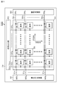
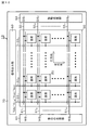
図1は、本開示の前提となるアクティブマトリクス型表示装置の基本的な構成の概略を示すシステム構成図である。本開示の前提となるアクティブマトリクス型表示装置は、特許文献1に記載の従来例に係るアクティブマトリクス型表示装置でもある。
<Active Matrix Display as a Premise of the Present Disclosure>
[System configuration]
FIG. 1 is a system configuration diagram illustrating an outline of a basic configuration of an active matrix display device as a premise of the present disclosure. The active matrix display device which is a premise of the present disclosure is also an active matrix display device according to a conventional example described in
アクティブマトリクス型表示装置は、電気光学素子に流れる電流を、当該電気光学素子と同じ画素回路内に設けた能動素子、例えば絶縁ゲート型電界効果トランジスタによって制御する表示装置である。絶縁ゲート型電界効果トランジスタとしては、典型的には、TFT(Thin Film Transistor;薄膜トランジスタ)を例示することができる。 The active matrix display device is a display device that controls the current flowing through the electro-optical element by an active element provided in the same pixel circuit as the electro-optical element, for example, an insulated gate field effect transistor. A typical example of the insulated gate field effect transistor is a TFT (Thin Film Transistor).
ここでは、デバイスに流れる電流値に応じて発光輝度が変化する電流駆動型の電気光学素子の一例である有機EL素子を、画素回路の発光部(発光素子)として用いるアクティブマトリクス型有機EL表示装置の場合を例に挙げて説明するものとする。以下では、「画素回路」を単に「画素」と記述する場合もある。 Here, an active matrix organic EL display device that uses, as a light emitting portion (light emitting element) of a pixel circuit, an organic EL element that is an example of a current-driven electro-optical element whose emission luminance changes according to a current value flowing through the device This case will be described as an example. Hereinafter, the “pixel circuit” may be simply referred to as “pixel”.
図1に示すように、本開示の前提となる有機EL表示装置100は、有機EL素子を含む複数の画素20が行列状に2次元配置されて成る画素アレイ部30と、当該画素アレイ部30の周辺に配置される駆動部とを有する構成となっている。駆動部は、例えば、画素アレイ部30と同じ表示パネル70上に搭載された書込み走査部40、駆動走査部50、及び、信号出力部60等から成り、画素アレイ部30の各画素20を駆動する。尚、書込み走査部40、駆動走査部50、及び、信号出力部60のいくつか、あるいは全部を表示パネル70外に設ける構成を採ることも可能である。
As shown in FIG. 1, an organic
ここで、有機EL表示装置100がカラー表示対応の表示装置の場合は、カラー画像を形成する単位となる1つの画素(単位画素/ピクセル)は複数の副画素(サブピクセル)から構成される。このとき、副画素の各々が図1の画素20に相当することになる。より具体的には、カラー表示対応の表示装置では、1つの画素は、例えば、赤色(Red;R)光を発光する副画素、緑色(Green;G)光を発光する副画素、青色(Blue;B)光を発光する副画素の3つの副画素から構成される。
Here, when the organic
但し、1つの画素としては、RGBの3原色の副画素の組み合わせに限られるものではなく、3原色の副画素に更に1色あるいは複数色の副画素を加えて1つの画素を構成することも可能である。より具体的には、例えば、輝度向上のために白色(White;W)光を発光する副画素を加えて1つの画素を構成したり、色再現範囲を拡大するために補色光を発光する少なくとも1つの副画素を加えて1つの画素を構成したりすることも可能である。 However, one pixel is not limited to a combination of RGB three primary color subpixels, and one pixel may be configured by adding one or more color subpixels to the three primary color subpixels. Is possible. More specifically, for example, one pixel is formed by adding a sub-pixel that emits white (W) light to improve luminance, or at least emits complementary color light to expand the color reproduction range. It is also possible to configure one pixel by adding one subpixel.
画素アレイ部30には、m行n列の画素20の配列に対して、行方向(画素行の画素の配列方向/水平方向)に沿って走査線31(311〜31m)と駆動線32(321〜32m)とが画素行毎に配線されている。更に、m行n列の画素20の配列に対して、列方向(画素列の画素の配列方向/垂直方向)に沿って信号線33(331〜33n)が画素列毎に配線されている。
The
走査線311〜31mは、書込み走査部40の対応する行の出力端にそれぞれ接続されている。駆動線321〜32mは、駆動走査部50の対応する行の出力端にそれぞれ接続されている。信号線331〜33nは、信号出力部60の対応する列の出力端にそれぞれ接続されている。
The scanning lines 31 1 to 31 m are connected to the output ends of the corresponding rows of the writing
書込み走査部40は、シフトレジスタ回路等によって構成されている。この書込み走査部40は、画素アレイ部30の各画素20への映像信号の信号電圧の書込みに際し、走査線31(311〜31m)に対して書込み走査信号WS(WS1〜WSm)を順次供給する。これにより、画素アレイ部30の各画素20を行単位で順番に走査する、所謂、線順次走査が行われる。
The
駆動走査部50は、書込み走査部40と同様に、シフトレジスタ回路等によって構成されている。この駆動走査部50は、書込み走査部40による線順次走査に同期して、駆動線32(321〜32m)に対して発光制御信号DS(DS1〜DSm)を供給することによって画素20の発光/非発光(消光)の制御を行う。
The
信号出力部60は、信号供給源(図示せず)から供給される輝度情報に応じた映像信号の信号電圧(以下、単に「信号電圧」と記述する場合もある)Vsigと基準電圧Vofsとを選択的に出力する。ここで、基準電圧Vofsは、映像信号の信号電圧Vsigの基準となる電圧(例えば、映像信号の黒レベルに相当する電圧)であり、後述する閾値補正に用いられる。
The
信号出力部60から択一的に出力される信号電圧Vsig/基準電圧Vofsは、信号線33(331〜33n)を介して画素アレイ部30の各画素20に対して、書込み走査部40による走査によって選択された画素行の単位で書き込まれる。すなわち、信号出力部60は、信号電圧Vsigを行(ライン)単位で書き込む線順次書込みの駆動形態を採っている。
The signal voltage V sig / reference voltage V ofs to be alternatively output from the
[画素回路]
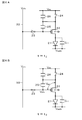
図2は、本開示の前提となるアクティブマトリクス型表示装置、即ち、従来例に係るアクティブマトリクス型表示装置における画素(画素回路)の回路例を示す回路図である。画素20の発光部は、有機EL素子21から成る。有機EL素子21は、デバイスに流れる電流値に応じて発光輝度が変化する電流駆動型の電気光学素子の一例である。
[Pixel circuit]
FIG. 2 is a circuit diagram illustrating a circuit example of a pixel (pixel circuit) in an active matrix display device as a premise of the present disclosure, that is, an active matrix display device according to a conventional example. The light emitting portion of the
図2に示すように、画素20は、有機EL素子21と、有機EL素子21に電流を流すことによって当該有機EL素子21を駆動する駆動回路とによって構成されている。有機EL素子21は、全ての画素20に対して共通に配線された共通電源線34にカソード電極が接続されている。
As shown in FIG. 2, the
有機EL素子21を駆動する駆動回路は、駆動トランジスタ22、サンプリングトランジスタ23、発光制御トランジスタ24、保持容量25、及び、補助容量26を有する構成となっている。尚、ガラス基板のような絶縁体上ではなく、シリコンのような半導体上に形成することを想定し、駆動トランジスタ22として、Pチャネル型のトランジスタを用いる構成を採っている。
A drive circuit for driving the
また、本例では、サンプリングトランジスタ23及び発光制御トランジスタ24についても、駆動トランジスタ22と同様に、Pチャネル型のトランジスタを用いる構成を採っている。従って、駆動トランジスタ22、サンプリングトランジスタ23、及び、発光制御トランジスタ24は、ソース/ゲート/ドレインの3端子ではなく、ソース/ゲート/ドレイン/バックゲートの4端子となっている。バックゲートには電源電圧Vddが印加される。
Further, in this example, the
但し、サンプリングトランジスタ23及び発光制御トランジスタ24については、スイッチ素子として機能するスイッチングトランジスタであることから、Pチャネル型のトランジスタに限られるものではない。従って、サンプリングトランジスタ23及び発光制御トランジスタ24は、Nチャネル型のトランジスタでも、Pチャネル型とNチャネル型が混在した構成のものでもよい。
However, the
上記の構成の画素20において、サンプリングトランジスタ23は、信号出力部60から信号線33を通して供給される信号電圧Vsigをサンプリングすることによって保持容量25に書き込む。発光制御トランジスタ24は、電源電圧Vddのノードと駆動トランジスタ22のソース電極との間に接続され、発光制御信号DSによる駆動の下に、有機EL素子21の発光/非発光を制御する。
In the
保持容量25は、駆動トランジスタ22のゲート電極とソース電極との間に接続されている。この保持容量25は、サンプリングトランジスタ23によるサンプリングによって書き込まれた信号電圧Vsigを保持する。駆動トランジスタ22は、保持容量25の保持電圧に応じた駆動電流を有機EL素子21に流すことによって有機EL素子21を駆動する。
The
補助容量26は、駆動トランジスタ22のソース電極と、固定電位のノード、例えば、電源電圧Vddのノードとの間に接続されている。この補助容量26は、信号電圧Vsigを書き込んだときに駆動トランジスタ22のソース電位が変動するのを抑制するとともに、駆動トランジスタ22のゲート−ソース間電圧Vgsを駆動トランジスタ22の閾値電圧Vthにする作用を為す。
The
[基本的な回路動作]
続いて、上記構成の本開示の前提となるアクティブマトリクス型有機EL表示装置100の基本的な回路動作について、図3のタイミング波形図を用いて説明する。
[Basic circuit operation]
Subsequently, a basic circuit operation of the active matrix organic
図3のタイミング波形図には、信号線33の電位Vofs/Vsig、発光制御信号DS、書込み走査信号WS、駆動トランジスタ22のソース電位Vs、ゲート電位Vg、及び、有機EL素子21のアノード電位Vanoのそれぞれの変化の様子を示している。図3のタイミング波形図では、ゲート電位Vgの波形については一点鎖線で図示している。
In the timing waveform diagram of FIG. 3, the potential V ofs / V sig of the
尚、サンプリングトランジスタ23及び発光制御トランジスタ24がPチャネル型であるため、書込み走査信号WS及び発光制御信号DSの低電位の状態がアクティブ状態となり、高電位の状態が非アクティブ状態となる。そして、サンプリングトランジスタ23及び発光制御トランジスタ24は、書込み走査信号WS及び発光制御信号DSのアクティブ状態で導通状態となり、非アクティブ状態で非導通状態となる。
Since the
時刻t8で、発光制御信号DSが非アクティブ状態となり、発光制御トランジスタ24が非導通状態となることで、保持容量25に保持されていた電荷が駆動トランジスタ22を通して放電される。そして、駆動トランジスタ22のゲート−ソース間電圧Vgsが、当該駆動トランジスタ22の閾値電圧Vth以下になると、駆動トランジスタ22がカットオフする。
At time t 8 , the light emission control signal DS becomes inactive and the light
駆動トランジスタ22がカットオフすると、有機EL素子21への電流供給の経路が遮断されるため、有機EL素子21のアノード電位Vanoが徐々に低下する。やがて、有機EL素子21のアノード電位Vanoが、有機EL素子21の閾値電圧Vthel以下になると、有機EL素子21が完全に消光状態となる。その後、時刻t1で、発光制御信号DSがアクティブ状態となり、発光制御トランジスタ24が導通状態となることで、次の1H期間(Hは1水平期間)に入る。これにより、t8−t1の期間が消光期間となる。
When the
発光制御トランジスタ24が導通状態となることで、駆動トランジスタ22のソース電極には電源電圧Vddが書き込まれる。そして、駆動トランジスタ22のソース電位Vsの上昇に連動して、ゲート電位Vgも上昇する。その後時刻t2で、書込み走査信号WSがアクティブ状態となることで、サンプリングトランジスタ23が導通状態になり、信号線33の電位をサンプリングする。このとき、信号線33には、基準電圧Vofsが供給された状態にある。従って、サンプリングトランジスタ23によるサンプリングによって、駆動トランジスタ22のゲート電極に基準電圧Vofsが書き込まれる。これにより、保持容量25には、(Vdd−Vofs)の電圧が保持される。
When the light
ここで、後述する閾値補正動作(閾値補正処理)を行うには、駆動トランジスタ22のゲート−ソース間電圧Vgsを、当該駆動トランジスタ22の閾値電圧Vthを超える電圧に設定しておく必要がある。そのため、|Vgs|=|Vdd−Vofs|>|Vth|となる関係に各電圧値が設定されることになる。
Here, in order to perform a threshold correction operation (threshold correction process) described later, it is necessary to set the gate-source voltage V gs of the
このように、駆動トランジスタ22のゲート電位Vgを基準電圧Vofsに設定する初期化動作が、次の閾値補正動作を行う前の準備(閾値補正準備)の動作である。従って、基準電圧Vofsが、駆動トランジスタ22のゲート電位Vgの初期化電圧ということになる。
Thus, the initialization operation for setting the gate potential V g of the
次に、時刻t3で、発光制御信号DSが非アクティブ状態になり、発光制御トランジスタ24が非導通状態になると、駆動トランジスタ22のソース電位Vsがフローティングとなる。そして、駆動トランジスタ22のゲート電位Vgが基準電圧Vofsに保たれた状態で閾値補正動作が開始される。すなわち、駆動トランジスタ22のゲート電位Vgから閾値電圧Vthを減じた電位(Vofs−Vth)に向けて、駆動トランジスタ22のソース電位Vsが下降(低下)を開始する。
Next, when the light emission control signal DS becomes inactive at time t 3 and the light
このように、駆動トランジスタ22のゲート電位Vgの初期化電圧Vofsを基準とし、当該初期化電圧Vofsから閾値電圧Vthを減じた電位(Vofs−Vth)に向けて駆動トランジスタ22のソース電位Vsを変化させる動作が閾値補正動作となる。この閾値補正動作が進むと、やがて、駆動トランジスタ22のゲート−ソース間電圧Vgsが、駆動トランジスタ22の閾値電圧Vthに収束する。この閾値電圧Vthに相当する電圧は保持容量25に保持される。このとき、駆動トランジスタ22のソース電位Vsは、Vs=Vofs−Vthとなる。
Thus, the driving
そして、時刻t4で、書込み走査信号WSが非アクティブ状態になり、サンプリングトランジスタ23が非導通状態になると、閾値補正期間が終了する。その後、信号出力部60から信号線33に映像信号の信号電圧Vsigが出力され、信号線33の電位が基準電圧Vofsから信号電圧Vsigに切り替わる。
Then, at time t 4 , when the write scanning signal WS becomes inactive and the
次に、時刻t5で、書込み走査信号WSがアクティブ状態になることで、サンプリングトランジスタ23が導通状態になり、信号電圧Vsigをサンプリングして画素20内に書き込む。このサンプリングトランジスタ23による信号電圧Vsigの書込み動作により、駆動トランジスタ22のゲート電位Vgが信号電圧Vsigになる。
Next, at time t 5 , the write scanning signal WS becomes active, whereby the
この映像信号の信号電圧Vsigの書込みの際に、駆動トランジスタ22のソース電極と電源電圧Vddのノードとの間に接続されている補助容量26は、駆動トランジスタ22のソース電位Vsが変動するのを抑える作用を為す。そして、映像信号の信号電圧Vsigによる駆動トランジスタ22の駆動の際に、当該駆動トランジスタ22の閾値電圧Vthが保持容量25に保持された閾値電圧Vthに相当する電圧と相殺される。
When the signal voltage V sig of the video signal is written, the
このとき、駆動トランジスタ22のゲート−ソース間電圧Vgsが、信号電圧Vsigに応じて拡大するが、駆動トランジスタ22のソース電位Vsは依然としてフローティングの状態にある。そのため、保持容量25の充電電荷は、駆動トランジスタ22の特性に応じて放電される。そして、このとき駆動トランジスタ22に流れる電流によって有機EL素子21の等価容量Celの充電が開始される。
At this time, the gate-source voltage V gs of the driving
有機EL素子21の等価容量Celが充電されることにより、駆動トランジスタ22のソース電位Vsが時間が経過するにつれて徐々に下降していく。このとき既に、駆動トランジスタ22の閾値電圧Vthの画素毎のばらつきがキャンセルされており、駆動トランジスタ22のドレイン−ソース間電流Idsは当該駆動トランジスタ22の移動度μに依存したものとなる。尚、駆動トランジスタ22の移動度μは、当該駆動トランジスタ22のチャネルを構成する半導体薄膜の移動度である。
As the equivalent capacitance C el of the
ここで、駆動トランジスタ22のソース電位Vsの下降分は、保持容量25の充電電荷を放電するように作用する。換言すれば、駆動トランジスタ22のソース電位Vsの下降分(変化量)は、保持容量25に対して負帰還がかけられたことになる。従って、駆動トランジスタ22のソース電位Vsの下降分は負帰還の帰還量となる。
Here, the decrease in the source potential V s of the
このように、駆動トランジスタ22に流れるドレイン−ソース間電流Idsに応じた帰還量で保持容量25に対して負帰還をかけることにより、駆動トランジスタ22のドレイン−ソース間電流Idsの移動度μに対する依存性を打ち消すことができる。この打ち消す動作(打ち消す処理)が、駆動トランジスタ22の移動度μの画素毎のばらつきを補正する移動度補正動作(移動度補正処理)である。
In this way, by applying negative feedback to the
より具体的には、駆動トランジスタ22のゲート電極に書き込まれる映像信号の信号振幅Vin(=Vsig−Vofs)が大きい程ドレイン−ソース間電流Idsが大きくなるため、負帰還の帰還量の絶対値も大きくなる。従って、映像信号の信号振幅Vin、即ち、発光輝度レベルに応じた移動度補正処理が行われる。また、映像信号の信号振幅Vinを一定とした場合、駆動トランジスタ22の移動度μが大きいほど負帰還の帰還量の絶対値も大きくなるため、画素毎の移動度μのばらつきを取り除くことができる。
More specifically, since the drain-source current I ds increases as the signal amplitude V in (= V sig −V ofs ) of the video signal written to the gate electrode of the
時刻t6で、書込み走査信号WSが非アクティブ状態になり、サンプリングトランジスタ23が非導通状態になることで、信号書込み&移動度補正期間が終了する。移動度補正を行った後、時刻t7で、発光制御信号DSがアクティブ状態になることで、発光制御トランジスタ24が導通状態になる。これにより、電源電圧Vddのノードから発光制御トランジスタ24を通して駆動トランジスタ22に電流が供給される。
At time t 6 , the write scan signal WS becomes inactive and the
このとき、サンプリングトランジスタ23が非導通状態にあることで、駆動トランジスタ22のゲート電極は信号線33から電気的に切り離されてフローティング状態にある。ここで、駆動トランジスタ22のゲート電極がフローティング状態にあるときは、駆動トランジスタ22のゲート−ソース間に保持容量25が接続されていることにより、駆動トランジスタ22のソース電位Vsの変動に連動してゲート電位Vgも変動する。
At this time, since the
すなわち、駆動トランジスタ22のソース電位Vs及びゲート電位Vgは、保持容量25に保持されているゲート−ソース間電圧Vgsを保持したまま上昇する。そして、駆動トランジスタ22のソース電位Vsは、トランジスタの飽和電流に応じた有機EL素子21の発光電圧Voledまで上昇する。
That is, the source potential V s and the gate potential V g of the
このように、駆動トランジスタ22のゲート電位Vgがソース電位Vsの変動に連動して変動する動作がブートストラップ動作である。換言すれば、ブートストラップ動作は、保持容量25に保持されたゲート−ソース間電圧Vgs、即ち、保持容量25の両端間電圧を保持したまま、駆動トランジスタ22のゲート電位Vg及びソース電位Vsが変動する動作である。
Thus, the operation in which the gate potential V g of the
そして、駆動トランジスタ22のドレイン−ソース間電流Idsが有機EL素子21に流れ始めることにより、当該電流Idsに応じて有機EL素子21のアノード電位Vanoが上昇する。やがて、有機EL素子21のアノード電位Vanoが有機EL素子21の閾値電圧Vthelを超えると、有機EL素子21に駆動電流が流れ始めるため、有機EL素子21が発光を開始する。
Then, when the drain-source current I ds of the driving
[閾値補正準備期間での不具合について]
ここで、閾値補正準備期間から閾値補正期間(時刻t2−時刻t4)にかけての動作点に着目する。先述した動作説明から明らかなように、閾値補正動作を行うには、駆動トランジスタ22のゲート−ソース間電圧Vgsを、当該駆動トランジスタ22の閾値電圧Vthを超える電圧に設定しておく必要がある。
[About defects in the threshold correction preparation period]
Here, attention is focused on the operating point from the threshold correction preparation period to the threshold correction period (time t 2 −time t 4 ). As is apparent from the above description of the operation, in order to perform the threshold correction operation, it is necessary to set the gate-source voltage V gs of the
そのために、駆動トランジスタ22に電流が流れ、図3のタイミング波形図に示すように、閾値補正準備期間から閾値補正期間の一部にかけて、一時的に、有機EL素子21のアノード電位Vanoが当該有機EL素子21の閾値電圧Vthelを超えてしまう。これにより、駆動トランジスタ22から有機EL素子21に数mA程度の貫通電流が流れることとなる。
Therefore, a current flows through the
そのため、閾値補正準備期間(閾値補正期間の開始の一部を含む)では、非発光期間であるにも拘わらず、信号電圧Vsigの階調に依らず毎フレーム、一定輝度で発光部(有機EL素子21)が発光してしまう。その結果、表示パネル70のコントラストの低下を招くことになる。
Therefore, in the threshold correction preparation period (including a part of the start of the threshold correction period), the light emitting unit (organic) has a constant luminance every frame regardless of the gradation of the signal voltage V sig in spite of the non-light emitting period. The EL element 21) emits light. As a result, the contrast of the
<実施形態の説明>
上記の不具合を解消するために、本開示の実施形態では次の構成を採る。すなわち、閾値補正の際に(閾値補正を行うに当たって)、駆動トランジスタ22のソース電極に第1の電圧を、ゲート電極に第1の電圧との差が閾値電圧Vthよりも小さい第2の電圧をそれぞれ書き込む。しかる後、駆動トランジスタ22のソース電極をフローティングにした状態でゲート電極に基準電圧Vofsを書き込む。この動作は、書込み走査部40、駆動走査部50、及び、信号出力部60等から成る駆動部による駆動の下に実行される。
<Description of Embodiment>
In order to solve the above problems, the embodiment of the present disclosure adopts the following configuration. That is, when threshold correction is performed (when threshold correction is performed), the first voltage is applied to the source electrode of the
本実施形態にあっては、第1の電圧として電源電圧Vddが用いられる。但し、電源電圧Vddに限られるものではない。第2の電圧については、以下、参照電圧Vrefと呼ぶこととする。本実施形態にあっては、参照電圧Vrefとして、Vref>Vdd−│Vth│の関係を満たす電圧が用いられる。 In the present embodiment, the power supply voltage V dd is used as the first voltage. However, the power supply voltage is not limited to Vdd . Hereinafter, the second voltage is referred to as a reference voltage V ref . In the present embodiment, a voltage satisfying the relationship of V ref > V dd − | V th | is used as the reference voltage V ref .
図4は、本開示の実施形態に係るアクティブマトリクス型表示装置の構成の概略を示すシステム構成図である。本実施形態においても、画素回路20の発光部(発光素子)として有機EL素子21を用いるアクティブマトリクス型有機EL表示装置の場合を例に挙げて説明するものとする。
FIG. 4 is a system configuration diagram illustrating an outline of the configuration of the active matrix display device according to the embodiment of the present disclosure. Also in this embodiment, the case of an active matrix organic EL display device using the
尚、本実施形態にあっては、画素回路(画素)20の駆動(駆動方法)を特徴としている。従って、画素回路20については、図2の画素回路と同じ構成となっている。すなわち、有機EL素子21を駆動する駆動回路は、Pチャネル型の駆動トランジスタ22を用いた3Tr(トランジスタ)の回路構成となっている。
In this embodiment, the pixel circuit (pixel) 20 is driven (driving method). Therefore, the
本実施形態に係るアクティブマトリクス型有機EL表示装置10にあっては、上記の駆動(駆動方法)を実現するために、信号出力部60は、信号線33に対して、閾値補正に用いる基準電圧Vofs、映像信号の信号電圧Vsig、及び、参照電圧Vrefを選択的に供給する構成となっている。すなわち、信号線33の電位は、Vofs/Vsig/Vrefの3値を選択的にとる。
In the active matrix organic EL display device 10 according to the present embodiment, the
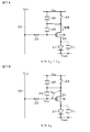
以下に、本実施形態に係るアクティブマトリクス型有機EL表示装置10の回路動作について、図5のタイミング波形図を用いて、図6−図8の動作説明図を参照しつつ説明する。尚、図6−図8の動作説明図では、図面の簡略化のために、サンプリングトランジスタ23及び発光制御トランジスタ24について、スイッチのシンボルを用いて図示している。
The circuit operation of the active matrix organic EL display device 10 according to the present embodiment will be described below with reference to the operation explanatory diagrams of FIGS. 6 to 8 using the timing waveform diagram of FIG. 6-8, the
消光期間(t8−t1)が終了し、時刻t2で、発光制御信号DSが非アクティブ状態となることで、図6Aに示すように、発光制御トランジスタ24が非導通状態となる。これにより、電源電圧Vddと駆動トランジスタ22のソース電極との間の電気的な接続が解除されるため、駆動トランジスタ22のソース電極はフローティングの状態になる。このとき、サンプリングトランジスタ23も非導通状態にある。
When the extinction period (t 8 -t 1 ) ends and the light emission control signal DS becomes inactive at time t 2 , the light
次に、時刻t3で、書込み走査信号WSがアクティブ状態となることで、図6Bに示すように、サンプリングトランジスタ23が導通状態になり、信号線33の電位をサンプリングする。このとき、信号線33には、基準電圧Vofsが供給された状態にある。従って、サンプリングトランジスタ23によるサンプリングによって、駆動トランジスタ22のゲート電極に基準電圧Vofsが書き込まれる。
Next, at time t 3 , the write scan signal WS becomes active, so that the
ここで、駆動トランジスタ22のソース電極がフローティングの状態にあるため、駆動トランジスタ22のソース電位Vsは、保持容量25及び補助容量26の容量比に応じた容量カップリングによってゲート電位Vgに追従して下降する。このとき、保持容量25の容量値をCsとし、補助容量26の容量値をCsubとすると、駆動トランジスタ22のソース電位Vsは、次式(1)で与えられる。
Vs=Vdd−{1−Csub/(Cs+Csub)}×(Vofs−Vdd) ・・・(1)
Here, since the source electrode of the driving
V s = V dd - {1 -C sub / (C s + C sub)} × (V ofs -V dd) ··· (1)
従って、駆動トランジスタ22のゲート−ソース間電圧Vgsは、
Vgs={Csub/(Cs+Csub)}×(Vofs−Vdd) ・・・(2)
となる。すなわち、保持容量25及び補助容量26の容量比に応じた容量カップリングによって、駆動トランジスタ22のゲート−ソース間電圧Vgsが拡大する。基準電圧Vofsの電圧値、並びに、保持容量25及び補助容量26の容量値Cs,Csubについては、Vgs>│Vth│の条件を満たすような値に設定する。これにより、駆動トランジスタ22のゲート−ソース間電圧Vgsは、閾値電圧Vthを超える電圧となる。
Therefore, the gate-source voltage V gs of the
V gs = {C sub / (C s + C sub )} × (V ofs −V dd ) (2)
It becomes. That is, the gate-source voltage V gs of the drive transistor 22 is expanded by capacitive coupling according to the capacitance ratio of the
閾値補正期間(t3−t4)では、図7Aに示すように、保持容量25に保持された電荷は、駆動トランジスタ22を通して放電される。そして、駆動トランジスタ22のソース電位VsがVofs+│Vth│になると、駆動トランジスタ22が非導通状態となり、閾値補正動作が終了する。これにより、保持容量25には、駆動トランジスタ22の│Vth│に相当する電圧が保持される。
In the threshold correction period (t 3 -t 4 ), the charge held in the
閾値補正期間(t3−t4)が終了した後、信号線33の電位が基準電圧Vofsから映像信号の信号電圧Vsigに切り替わる。その後、時刻t5で、書込み走査信号WSがアクティブ状態になることで、図7Bに示すように、サンプリングトランジスタ23が再度導通状態になる。そして、サンプリングトランジスタ23によるサンプリングによって、駆動トランジスタ22のゲート電極に信号電圧Vsigが書き込まれる。
After the threshold correction period (t 3 -t 4 ) ends, the potential of the
このとき、駆動トランジスタ22のソース電極がフローティングの状態にあるため、保持容量25及び補助容量26の容量比に応じた容量カップリングによって、駆動トランジスタ22のソース電位Vsがゲート電位Vgに追従する。このとき、駆動トランジスタ22のゲート−ソース間電圧Vgsは、
Vgs={Csub/(Cs+Csub)}×(Vofs-Vsig)+│Vth│ ・・・(3)
になる。
At this time, since the source electrode of the driving
V gs = {C sub / ( C s + C sub)} × (V ofs -V sig) + │V th │ ··· (3)
become.
この信号書込み期間では、駆動トランジスタ22を介して電流が流れるため、先述したアクティブマトリクス型有機EL表示装置100の動作の場合と同様に、信号電圧Vsigの書込みを行いながら移動度補正が行われる。移動度補正の際の動作については、先述した通りである。この信号書込み&移動度補正期間(t5−t6)は、数100ナノ秒〜数マイクロ秒と非常に短い時間となる。
In this signal writing period, a current flows through the driving
信号書込み&移動度補正期間(t5−t6)が終了した後、時刻t7で、発光制御信号DSがアクティブ状態になることで、図8Aに示すように、発光制御トランジスタ24が導通状態になる。これにより、電源電圧Vddのノードから発光制御トランジスタ24を通して駆動トランジスタ22に電流Idsが流れる。このとき、先述したブートストラップ動作が行われる。そして、有機EL素子21のアノード電位Vanoが有機EL素子21の閾値電圧Vthelを超えると、有機EL素子21に駆動電流が流れ始めるため、有機EL素子21が発光を開始する。
After the signal writing & mobility correction period (t 5 -t 6 ) ends, the light emission control signal DS becomes active at time t 7 , so that the light
このとき、駆動トランジスタ22の閾値電圧Vthと移動度μの画素毎のばらつきの補正が行われた状態にあるため、トランジスタ特性のばらつきの無い、ユニフォーミティの高い画質を得ることができる。また、発光期間では、駆動トランジスタ22のソース電位Vsが電源電圧Vddまで上昇し、そのゲート電位Vgも保持容量25を介して追従し、同様に上昇する。
At this time, since the variation of the threshold voltage V th and mobility μ of the driving
発光期間において、信号線33の電位が映像信号の信号電圧Vsigから参照電圧Vrefに切り替わる。そして、消光期間に入る時刻t8で、書込み走査信号WSがアクティブ状態になることで、図8Bに示すように、サンプリングトランジスタ23が導通状態になる。そして、サンプリングトランジスタ23によるサンプリングによって参照電圧Vrefが駆動トランジスタ22のゲート電極に書き込まれる。このとき、発光制御トランジスタ24が導通状態にあることで、駆動トランジスタ22のソース電極には電源電圧Vddが書き込まれている。従って、駆動トランジスタ22のゲート−ソース間電圧Vgsは、Vgs=Vdd−Vrefとなる。
In the light emission period, the potential of the
ここで、参照電圧VrefをVdd−Vref<│Vth│の関係を満たす値に設定することで、駆動トランジスタ22を非導通状態にすることが可能となる。そして、駆動トランジスタ22が非導通状態になることで、有機EL素子21への電流の供給が停止するため、有機EL素子21が消光する。
Here, by setting the reference voltage V ref to a value satisfying the relationship of V dd −V ref <| V th |, the
上述した一連の回路動作において、閾値補正、信号書込み&移動度補正、発光、及び、消光の各動作は、例えば1水平期間(1H)において実行される。 In the series of circuit operations described above, the threshold correction, signal writing & mobility correction, light emission, and extinction operations are executed, for example, in one horizontal period (1H).
尚、ここでは、閾値補正処理を1回だけ実行する駆動法を採る場合を例に挙げて説明したが、この駆動法は一例に過ぎず、この駆動法に限られるものではない。例えば、閾値補正を移動度補正及び信号書込みと共に行う1H期間に加えて、当該1H期間に先行する複数の水平期間に亘って分割して閾値補正を複数回実行する、所謂、分割閾値補正を行う駆動法を採ることも可能である。 Here, the case where the driving method in which the threshold value correction process is executed only once is described as an example, but this driving method is only an example and is not limited to this driving method. For example, in addition to the 1H period in which threshold correction is performed together with mobility correction and signal writing, so-called divided threshold correction is performed in which threshold correction is performed a plurality of times by being divided over a plurality of horizontal periods preceding the 1H period. It is also possible to adopt a driving method.
この分割閾値補正の駆動法によれば、高精細化に伴う多画素化によって1水平期間として割り当てられる時間が短くなったとしても、閾値補正期間として複数の水平期間に亘って十分な時間を確保することができる。従って、1水平期間として割り当てられる時間が短くなっても、閾値補正期間として十分な時間を確保できるため、閾値補正処理を確実に実行できることになる。 According to this division threshold correction driving method, sufficient time is secured over a plurality of horizontal periods as a threshold correction period even if the time allocated as one horizontal period is shortened due to the increase in the number of pixels accompanying high definition. can do. Therefore, even if the time allocated as one horizontal period is shortened, a sufficient time can be secured as the threshold correction period, so that the threshold correction process can be reliably executed.
以上説明した、Pチャネル型の駆動トランジスタ22を用いた3Trの画素回路では、駆動トランジスタ22としてNチャネル型のトランジスタを用いる場合に比べて、トランジスタのばらつきを抑制できる。そして、当該3Trの画素回路において、消光動作及び容量カップリングを用いた閾値補正動作を行うことで、非発光期間での有機EL素子21への貫通電流を抑制できるため、コントラストを維持したままユニフォーミティの高い画質を得ることができる。
In the 3Tr pixel circuit using the P-channel
より具体的には、駆動トランジスタ22のソース電極に電源電圧Vddを、ゲート電極にVdd−Vref<│Vth│の関係を満たす参照電圧Vrefをそれぞれ書き込むことで、駆動トランジスタ22のゲート−ソース間電圧Vgsが閾値電圧Vthよりも小さくなる。このとき、駆動トランジスタ22が非導通状態となり、有機EL素子21への電流の供給が行われないため、有機EL素子21は消光状態となる(消光動作)。
More specifically, the power supply voltage V dd is written in the source electrode of the
その後、ソース電極がフローティングの状態にある駆動トランジスタ22のゲート電極に基準電圧Vofsを書き込むことで、保持容量25及び補助容量26の容量比に応じた容量カップリングによって、駆動トランジスタ22のソース電位Vsがゲート電位Vgに追従して下降する。これにより、駆動トランジスタ22のゲート−ソース間電圧Vgsが閾値電圧Vth以上に拡大する。従って、貫通電流が流れる閾値補正準備期間を設けなくて済むため、非発光期間での有機EL素子21への貫通電流を抑制できる。その結果、コントラストを維持したままユニフォーミティの高い画質を得ることができる。
After that, by writing the reference voltage V ofs to the gate electrode of the
保持容量25及び補助容量26の各容量値Cs,Csubについては、先述したVgs>│Vth│の条件を満たす限りにおいて任意に設定可能である。但し、Cs≧Csubの関係に設定することで、駆動トランジスタ22のゲート−ソース間電圧Vgsを小さくできるため、駆動トランジスタ22に流れる電流を小さくすることができる。
The capacitance values C s and C sub of the
また、本実施形態に係る画素回路では、回路動作点として、最大かかる電圧が(Vdd−Vsig)であり、これは例えば4[V]程度の電圧であり、画素回路として非常に小さい(低い)。これにより、画素回路を構成するトランジスタの耐圧、また、容量素子に要求される耐圧に対してマージンを得ることができるため、絶縁膜の薄膜化及び保持容量25や補助容量26への高誘電率材料の適用などを容易に行うことができる。保持容量25や補助容量26を構成する高誘電率材料としては、シリコン窒化膜(SiN)、酸化チタン(TaO)、酸化ハフニウム(HfO)などを例示することができる。
In the pixel circuit according to the present embodiment, the maximum voltage applied as a circuit operating point is (V dd −V sig ), which is a voltage of about 4 [V], for example, and is extremely small as the pixel circuit ( Low). Accordingly, a margin can be obtained for the withstand voltage of the transistors constituting the pixel circuit and the withstand voltage required for the capacitor, so that the insulating film is thinned and the dielectric constant to the
<変形例>
本開示の技術は、上記の実施形態に限定されるものではなく、本開示の要旨を逸脱しない範囲内で種々の変形、改変が可能である。例えば、上記の実施形態では、画素20を構成するPチャネル型のトランジスタをシリコンのような半導体上に形成して成る表示装置に適用した場合を例に挙げて説明したが、画素20を構成するPチャネル型のトランジスタをガラス基板のような絶縁体上に形成して成る表示装置に対しても、本開示の技術を適用することができる。
<Modification>
The technology of the present disclosure is not limited to the above-described embodiment, and various modifications and changes can be made without departing from the gist of the present disclosure. For example, in the above embodiment, the case where the
また、上記の実施形態では、基準電圧Vofs及び参照電圧Vrefを信号線33からサンプリングトランジスタ23によるサンプリングによって画素回路20内に選択的に書き込むとしたが、これに限られるものではない。すなわち、基準電圧Vofs及び参照電圧Vrefをそれぞれ独立に書き込む専用のトランジスタを画素回路20内に設ける構成を採ることも可能である。
In the above embodiment, the reference voltage V ofs and the reference voltage V ref are selectively written into the
[変形例1]
上記の実施形態では、参照電圧Vrefについて、Vref>Vdd−Vthの関係を満たす電圧を用いるとしたが、当該条件を満たす限りにおいて、参照電圧Vrefが画素回路20の電源電圧Vddと異なる電圧であってもよいが、同じ電圧である方が好ましい。参照電圧Vrefを電源電圧Vddと同じ電圧とすることで、参照電圧Vrefを生成するために専用の電源を設ける必要がなくなるため、システム構成の簡略化を図ることができる、というメリットがある。
[Modification 1]
In the above embodiment, the reference voltage V ref, V ref> V dd is set to use a voltage that satisfies the relationship of -V th, as long as the condition is satisfied, the reference voltage V ref of the
[変形例2]
上記の実施形態では、信号線33に対して参照電圧Vrefを書き込む際に、映像信号の信号電圧Vsigから直接参照電圧Vrefに切り替える構成としたが、参照電圧Vrefを書き込むのに先立って、信号電圧Vsigと参照電圧Vrefとの間の中間電圧Vmidを書き込む構成を採ることも可能である。
[Modification 2]
In the above embodiment, when writing the reference voltage V ref to the
信号電圧Vsigから直接参照電圧Vrefに切り替える場合、信号線33の電位がVsigからVrefへと大きく遷移するため、図9に示すように、信号線33の電位にオーバーシュートが発生する場合がある。遷移時にオーバーシュートが発生すると、有機EL素子21の発光中に非導通状態にあるサンプリングトランジスタ23のゲート電位Vg、ドレイン電位Vd、ソース電位Vs(信号線33の電位でもある)の電位関係が崩れてしまう。
When the signal voltage V sig is directly switched to the reference voltage V ref , the potential of the
具体的には、発光中の駆動トランジスタ22のゲート電位をVA、オーバーシュート電位をVoverとすると、サンプリングトランジスタ23の電位関係が、Vg=Vdd、Vd=VA、Vs=Vdd+Voverとなる。そして、Vgs=Vover>│Vth│となった際に、サンプリングトランジスタ23が一瞬導通状態になってしまう。すると、発光中にも関わらず参照電圧Vrefが駆動トランジスタ22のゲート電極に書き込まれることになるため、輝度が低下し、有機EL素子21が消光してしまう懸念がある。
Specifically, when the gate potential of the driving
このような不具合を解消するために為されたのが変形例2である。具体的には、図10のシステム構成図に示すように、信号出力部60は、信号線33に対して、閾値補正に用いる基準電圧Vofs、映像信号の信号電圧Vsig、参照電圧Vref、及び、信号電圧Vsigと参照電圧Vrefとの間の中間電圧Vmidを選択的に供給する構成となっている。すなわち、信号線33の電位は、Vofs/Vsig/Vref/Vmidの4値をとる。
Modification 2 is made to solve such a problem. Specifically, as illustrated in the system configuration diagram of FIG. 10, the
そして、図11のタイミング波形図に示すように、映像信号の信号電圧Vsigから直接参照電圧Vrefに切り替える際に、Vsig⇒Vmid⇒Vrefという具合に中間電圧Vmidを経由した切替えを行うことで、オーバーシュートの発生を抑制することができる。これにより、サンプリングトランジスタ23を使用した消光動作の不具合である輝度劣化を無くすことが可能となる。
Then, as shown in the timing waveform diagram of FIG. 11, when switching from the signal voltage V sig of the video signal directly to the reference voltage V ref , switching via the intermediate voltage V mid such as V sig ⇒ V mid ⇒ V ref. By performing the above, occurrence of overshoot can be suppressed. As a result, it is possible to eliminate luminance degradation that is a defect of the quenching operation using the
また、変形例2を採用するに当たって、中間電圧Vmidとして基準電圧Vofsを利用することで、中間電圧Vmidを生成するために専用の電源を設ける必要がなくなるため、システム構成の簡略化を図ることができる。 Further, when adopting the second modification, the use of the reference voltage V ofs as the intermediate voltage V mid, since the need to provide a dedicated power supply for generating an intermediate voltage V mid is eliminated, simplifying the system configuration Can be planned.
<電子機器>
以上説明した本開示の表示装置は、電子機器に入力された映像信号、若しくは、電子機器内で生成した映像信号を、画像若しくは映像として表示するあらゆる分野の電子機器において、その表示部(表示装置)として用いることが可能である。
<Electronic equipment>
The display device of the present disclosure described above is a display unit (display device) in an electronic device of any field that displays a video signal input to an electronic device or a video signal generated in the electronic device as an image or a video. ).
上述した実施形態の説明から明らかなように、本開示の表示装置は、非発光期間では発光部を確実に非発光の状態に制御することができるため、表示パネルの高コントラスト化を図ることができる。従って、あらゆる分野の電子機器において、その表示部として本開示の表示装置を用いることで、表示部の高コントラスト化を実現できることになる。 As is apparent from the description of the above-described embodiment, the display device of the present disclosure can reliably control the light emitting unit to be in a non-light emitting state during the non-light emitting period, so that the display panel can have high contrast. it can. Therefore, high-contrast of the display unit can be realized by using the display device of the present disclosure as the display unit in electronic devices in all fields.
本開示の表示装置を表示部に用いる電子機器としては、テレビジョンシステムの他、例えば、ヘッドマウントディスプレイ、デジタルカメラ、ビデオカメラ、ゲーム機器、ノート型パーソナルコンピュータなどを例示することができる。また、本開示の表示装置は、電子書籍機器や電子腕時計等の携帯情報機器や、携帯電話機やPDA等の携帯通信機器などの電子機器において、その表示部として用いることもできる。 As an electronic device using the display device of the present disclosure for a display unit, for example, a head mounted display, a digital camera, a video camera, a game device, a notebook personal computer, and the like can be exemplified in addition to a television system. The display device of the present disclosure can also be used as a display unit in electronic devices such as portable information devices such as electronic book devices and electronic watches, and portable communication devices such as mobile phones and PDAs.
尚、本開示は以下のような構成をとることもできる。
[1]発光部を駆動するPチャネル型の駆動トランジスタ、信号電圧を書き込むサンプリングトランジスタ、発光部の発光/非発光を制御する発光制御トランジスタ、駆動トランジスタのゲート電極とソース電極との間に接続された保持容量、及び、駆動トランジスタのソース電極に接続された補助容量を含む画素回路が配置されて成る画素アレイ部と、
閾値補正の際に、駆動トランジスタのソース電極に第1の電圧を、ゲート電極に第1の電圧との差が駆動トランジスタの閾値電圧よりも小さい第2の電圧をそれぞれ書き込み、しかる後、駆動トランジスタのソース電極をフローティングにした状態でゲート電極に対して閾値補正に用いる基準電圧を書き込む駆動を行う駆動部と、
を備える表示装置。
[2]第1の電圧は、画素の電源電圧である上記[1]に記載の表示装置。
[3]発光制御トランジスタは、電源電圧のノードと駆動トランジスタのソース電極との間に接続されており、
駆動部は、発光制御トランジスタを導通状態にすることによって駆動トランジスタのソース電極に電源電圧を書き込み、発光制御トランジスタを非導通状態にすることによって駆動トランジスタのソース電極をフローティングの状態にする上記[2]に記載の表示装置。
[4]第2の電圧は、画素の電源電圧と同じである上記[1]から上記[3]のいずれかに記載の表示装置。
[5]第2の電圧は、画素の電源電圧と異なる電圧である上記[1]から上記[3]のいずれかに記載の表示装置。
[6]サンプリングトランジスタは、信号線と駆動トランジスタのゲート電極との間に接続されており、
駆動部は、信号線を通して与えられる第2の電圧を、サンプリングトランジスタのサンプリングによって書き込む上記[1]から上記[5]のいずれかに記載の表示装置。
[7]サンプリングトランジスタは、信号線と駆動トランジスタのゲート電極との間に接続されており、
駆動部は、信号線を通して与えられる基準電圧を、サンプリングトランジスタのサンプリングによって書き込む上記[1]から上記[5]のいずれかに記載の表示装置。
[8]駆動部は、基準電圧を書き込んだときの保持容量及び補助容量による容量カップリングによって駆動トランジスタのソース電位を上げる上記[1]から上記[7]のいずれかに記載の表示装置。
[9]駆動部は、基準電圧を書き込んだときの保持容量及び補助容量による容量カップリングによって駆動トランジスタのゲート−ソース間電圧を拡大する上記[1]から上記[7]のいずれかに記載の表示装置。
[10]保持容量の容量値は、補助容量の容量値以上である上記[1]から上記[9]のいずれかに記載の表示装置。
[11]画素回路の動作点として、最大かかる電圧が(電源電圧−信号電圧)である上記[1]から上記[10]のいずれかにに記載の表示装置。
[12]保持容量は、高誘電率材料から成る上記[11]に記載の表示装置。
[13]補助容量は、高誘電率材料から成る上記[11]に記載の表示装置。
[14] 第2の電圧は、信号線に書き込まれ、サンプリングトランジスタによってサンプリングされる電圧であり、
信号線に対して第2の電圧を書き込むのに先立って、第2の電圧と信号電圧との間の中間電圧を書き込む上記[1]から上記[13]のいずれかに記載の表示装置。
[15]中間電圧は、基準電圧である上記[14]に記載の表示装置。
[16]発光部は、デバイスに流れる電流値に応じて発光輝度が変化する電流駆動型の電気光学素子から構成されている上記[1]から上記[15]のいずれかに記載の表示装置。
[17]電流駆動型の電気光学素子は、有機エレクトロルミネッセンス素子である上記[16]に記載の表示装置。
[18]サンプリングトランジスタ及び発光制御トランジスタは、Pチャネル型のトランジスタから成る上記[1]から上記[17]のいずれかに記載の表示装置。
[19]発光部を駆動するPチャネル型の駆動トランジスタ、信号電圧を書き込むサンプリングトランジスタ、発光部の発光/非発光を制御する発光制御トランジスタ、駆動トランジスタのゲート電極とソース電極との間に接続された保持容量、及び、駆動トランジスタのソース電極に接続された補助容量を含む画素回路が配置されて成る表示装置の駆動に当たって、
閾値補正の際に、
駆動トランジスタのソース電極に第1の電圧を、ゲート電極に第1の電圧との差が駆動トランジスタの閾値電圧よりも小さい第2の電圧をそれぞれ書き込み、
次いで、駆動トランジスタのソース電極をフローティングにし、
しかる後、駆動トランジスタのゲート電極に対して閾値補正に用いる基準電圧を書き込む表示装置の駆動方法。
[20]発光部を駆動するPチャネル型の駆動トランジスタ、信号電圧を書き込むサンプリングトランジスタ、発光部の発光/非発光を制御する発光制御トランジスタ、駆動トランジスタのゲート電極とソース電極との間に接続された保持容量、及び、駆動トランジスタのソース電極に接続された補助容量を含む画素回路が配置されて成る画素アレイ部と、
閾値補正の際に、駆動トランジスタのソース電極に第1の電圧を、ゲート電極に第1の電圧との差が駆動トランジスタの閾値電圧よりも小さい第2の電圧をそれぞれ書き込み、しかる後、駆動トランジスタのソース電極をフローティングにした状態でゲート電極に対して閾値補正に用いる基準電圧を書き込む駆動を行う駆動部と、
を備える表示装置を有する電子機器。
In addition, this indication can also take the following structures.
[1] A P-channel driving transistor for driving the light emitting unit, a sampling transistor for writing a signal voltage, a light emission control transistor for controlling light emission / non-emission of the light emitting unit, and connected between the gate electrode and the source electrode of the driving transistor. A pixel array unit in which a pixel circuit including a storage capacitor and an auxiliary capacitor connected to the source electrode of the driving transistor is disposed;
At the time of threshold correction, a first voltage is written to the source electrode of the driving transistor, and a second voltage whose difference from the first voltage is smaller than the threshold voltage of the driving transistor is written to the gate electrode. A driving unit for driving to write a reference voltage used for threshold correction to the gate electrode in a state where the source electrode is in a floating state,
A display device comprising:
[2] The display device according to [1], wherein the first voltage is a power supply voltage of the pixel.
[3] The light emission control transistor is connected between the node of the power supply voltage and the source electrode of the drive transistor,
The drive unit writes the power supply voltage to the source electrode of the drive transistor by turning on the light emission control transistor, and sets the source electrode of the drive transistor in the floating state by turning off the light emission control transistor [2]. ] The display apparatus as described in.
[4] The display device according to any one of [1] to [3], wherein the second voltage is the same as a power supply voltage of the pixel.
[5] The display device according to any one of [1] to [3], wherein the second voltage is a voltage different from a power supply voltage of the pixel.
[6] The sampling transistor is connected between the signal line and the gate electrode of the driving transistor,
The display device according to any one of [1] to [5], wherein the driving unit writes the second voltage applied through the signal line by sampling of the sampling transistor.
[7] Sa pump ring transistor is connected between the gate electrode of the signal line and the driving transistor,
The display device according to any one of [1] to [5], wherein the driving unit writes the reference voltage applied through the signal line by sampling of the sampling transistor.
[8] The display device according to any one of [1] to [7], wherein the driving unit raises a source potential of the driving transistor by capacitive coupling using a storage capacitor and an auxiliary capacitor when the reference voltage is written.
[9] The driving unit according to any one of [1] to [7], wherein the driving unit expands a gate-source voltage of the driving transistor by capacitive coupling using a storage capacitor and an auxiliary capacitor when the reference voltage is written. Display device.
[10] The display device according to any one of [1] to [9], wherein a capacitance value of the storage capacitor is equal to or greater than a capacitance value of the auxiliary capacitor.
[11] The display device according to any one of [1] to [10], wherein the maximum applied voltage is (power supply voltage−signal voltage) as an operating point of the pixel circuit.
[12] The display device according to [11], wherein the storage capacitor is made of a high dielectric constant material.
[13] The display device according to [11], wherein the auxiliary capacitor is made of a high dielectric constant material.
[14] The second voltage is a voltage written to the signal line and sampled by the sampling transistor,
The display device according to any one of [1] to [13], wherein an intermediate voltage between the second voltage and the signal voltage is written before writing the second voltage to the signal line.
[15] The display device according to [14], wherein the intermediate voltage is a reference voltage.
[16] The display device according to any one of [1] to [15], wherein the light-emitting unit includes a current-driven electro-optic element whose emission luminance changes according to a current value flowing through the device.
[17] The display device according to [16], wherein the current-driven electro-optic element is an organic electroluminescence element.
[18] The display device according to any one of [1] to [17], wherein the sampling transistor and the light emission control transistor are P-channel transistors.
[19] A P-channel driving transistor for driving the light emitting section, a sampling transistor for writing a signal voltage, a light emission control transistor for controlling light emission / non-light emission of the light emitting section, and connected between the gate electrode and the source electrode of the driving transistor. In driving a display device in which a pixel circuit including a storage capacitor and an auxiliary capacitor connected to a source electrode of a driving transistor is arranged,
During threshold correction,
A first voltage is written to the source electrode of the driving transistor, and a second voltage whose difference from the first voltage is smaller than the threshold voltage of the driving transistor is written to the gate electrode,
Next, the source electrode of the drive transistor is floated,
Thereafter, a display device driving method for writing a reference voltage used for threshold correction to the gate electrode of the driving transistor.
[20] A P-channel type driving transistor for driving the light emitting unit, a sampling transistor for writing a signal voltage, a light emission control transistor for controlling light emission / non-light emission of the light emitting unit, and connected between the gate electrode and the source electrode of the driving transistor. A pixel array unit in which a pixel circuit including a storage capacitor and an auxiliary capacitor connected to the source electrode of the driving transistor is disposed;
At the time of threshold correction, a first voltage is written to the source electrode of the driving transistor, and a second voltage whose difference from the first voltage is smaller than the threshold voltage of the driving transistor is written to the gate electrode. A driving unit for driving to write a reference voltage used for threshold correction to the gate electrode in a state where the source electrode is in a floating state,
An electronic apparatus having a display device.
10,100・・・有機EL表示装置、20・・・画素(画素回路)、21・・・有機EL素子、22・・・駆動トランジスタ、23・・・サンプリングトランジスタ、24・・・発光制御トランジスタ、25・・・保持容量、26・・・補助容量、30・・・画素アレイ部、31(311〜31m)・・・走査線、32(321〜32m)・・・駆動線、33(331〜33n)・・・信号線、34・・・共通電源線、40・・・書込み走査部、50・・・駆動走査部、60・・・信号出力部、70・・・表示パネル DESCRIPTION OF SYMBOLS 10,100 ... Organic EL display device, 20 ... Pixel (pixel circuit), 21 ... Organic EL element, 22 ... Drive transistor, 23 ... Sampling transistor, 24 ... Light emission control transistor , 25 ... holding capacity, 26 ... auxiliary capacity, 30 ... pixel array section, 31 (31 1 to 31 m ) ... scanning line, 32 (32 1 to 32 m ) ... drive line 33 (33 1 to 33 n )... Signal line, 34... Common power supply line, 40... Write scanning unit, 50... Drive scanning unit, 60.・ Display panel
Claims (19)
閾値補正の際に、駆動トランジスタのソース電極に第1の電圧を、ゲート電極に第1の電圧との差が駆動トランジスタの閾値電圧よりも小さい第2の電圧をそれぞれ書き込み、しかる後、駆動トランジスタのソース電極をフローティングにした状態でゲート電極に対して閾値補正に用いる基準電圧を書き込む駆動を行う駆動部と、
を備え、
第2の電圧は、信号線に書き込まれ、サンプリングトランジスタによってサンプリングされる電圧であり、
駆動部は、信号線に対して第2の電圧を書き込むのに先立って、第2の電圧と信号電圧との間の中間電圧を書き込む表示装置。 A P-channel type driving transistor for driving the light emitting unit, a sampling transistor connected between the signal line and the gate electrode of the driving transistor, for writing a signal voltage supplied through the signal line , a node for the power supply voltage, and a source electrode of the driving transistor Is connected between and a light emission control transistor that controls light emission / non-light emission of the light emitting unit, a storage capacitor that is connected between the gate electrode and the source electrode of the drive transistor and holds a voltage corresponding to the threshold voltage of the drive transistor And a pixel array unit in which a pixel circuit including an auxiliary capacitor connected between a source electrode of the driving transistor and a node of a fixed potential is disposed;
At the time of threshold correction, a first voltage is written to the source electrode of the driving transistor, and a second voltage whose difference from the first voltage is smaller than the threshold voltage of the driving transistor is written to the gate electrode. A driving unit for driving to write a reference voltage used for threshold correction to the gate electrode in a state where the source electrode is in a floating state,
Equipped with a,
The second voltage is a voltage written to the signal line and sampled by the sampling transistor,
The drive unit writes the intermediate voltage between the second voltage and the signal voltage prior to writing the second voltage to the signal line .
閾値補正の際に、
駆動トランジスタのソース電極に第1の電圧を、ゲート電極に第1の電圧との差が駆動トランジスタの閾値電圧よりも小さい第2の電圧をそれぞれ書き込み、
次いで、駆動トランジスタのソース電極をフローティングにし、
しかる後、駆動トランジスタのゲート電極に対して閾値補正に用いる基準電圧を書き込み、
第2の電圧は、信号線に書き込まれ、サンプリングトランジスタによってサンプリングされる電圧であり、
信号線に対して第2の電圧を書き込むのに先立って、第2の電圧と信号電圧との間の中間電圧を書き込む表示装置の駆動方法。 A P-channel type driving transistor for driving the light emitting unit, a sampling transistor connected between the signal line and the gate electrode of the driving transistor, for writing a signal voltage supplied through the signal line , a node for the power supply voltage, and a source electrode of the driving transistor Is connected between and a light emission control transistor that controls light emission / non-light emission of the light emitting unit, a storage capacitor that is connected between the gate electrode and the source electrode of the drive transistor and holds a voltage corresponding to the threshold voltage of the drive transistor And driving a display device in which a pixel circuit including an auxiliary capacitor connected between a source electrode of a driving transistor and a node of a fixed potential is arranged.
During threshold correction,
A first voltage is written to the source electrode of the driving transistor, and a second voltage whose difference from the first voltage is smaller than the threshold voltage of the driving transistor is written to the gate electrode,
Next, the source electrode of the drive transistor is floated,
Thereafter, write the reference voltage used for threshold correction to the gate electrode of the driving transistor,
The second voltage is a voltage written to the signal line and sampled by the sampling transistor,
A method for driving a display device, in which an intermediate voltage between a second voltage and a signal voltage is written prior to writing a second voltage to a signal line .
閾値補正の際に、駆動トランジスタのソース電極に第1の電圧を、ゲート電極に第1の電圧との差が駆動トランジスタの閾値電圧よりも小さい第2の電圧をそれぞれ書き込み、しかる後、駆動トランジスタのソース電極をフローティングにした状態でゲート電極に対して閾値補正に用いる基準電圧を書き込む駆動を行う駆動部と、
を備え、
第2の電圧は、信号線に書き込まれ、サンプリングトランジスタによってサンプリングされる電圧であり、
駆動部は、信号線に対して第2の電圧を書き込むのに先立って、第2の電圧と信号電圧との間の中間電圧を書き込む表示装置を有する電子機器。 A P-channel type driving transistor for driving the light emitting unit, a sampling transistor connected between the signal line and the gate electrode of the driving transistor, for writing a signal voltage supplied through the signal line , a node for the power supply voltage, and a source electrode of the driving transistor Is connected between and a light emission control transistor that controls light emission / non-light emission of the light emitting unit, a storage capacitor that is connected between the gate electrode and the source electrode of the drive transistor and holds a voltage corresponding to the threshold voltage of the drive transistor And a pixel array unit in which a pixel circuit including an auxiliary capacitor connected between a source electrode of the driving transistor and a node of a fixed potential is disposed;
At the time of threshold correction, a first voltage is written to the source electrode of the driving transistor, and a second voltage whose difference from the first voltage is smaller than the threshold voltage of the driving transistor is written to the gate electrode. A driving unit for driving to write a reference voltage used for threshold correction to the gate electrode in a state where the source electrode is in a floating state,
Equipped with a,
The second voltage is a voltage written to the signal line and sampled by the sampling transistor,
The electronic device having a display device in which the driving unit writes an intermediate voltage between the second voltage and the signal voltage before writing the second voltage to the signal line .
Priority Applications (8)
| Application Number | Priority Date | Filing Date | Title |
|---|---|---|---|
| JP2013142831A JP6201465B2 (en) | 2013-07-08 | 2013-07-08 | Display device, driving method of display device, and electronic apparatus |
| US14/289,259 US10621911B2 (en) | 2013-07-08 | 2014-05-28 | Display device, driving method for display device and electronic apparatus |
| CN201910181452.7A CN110097848B (en) | 2013-07-08 | 2014-07-01 | Display device, driving method for display device, and electronic apparatus |
| CN201410311252.6A CN104282257B (en) | 2013-07-08 | 2014-07-01 | Display device, driving method and electronic equipment for display device |
| CN201910182088.6A CN109920376A (en) | 2013-07-08 | 2014-07-01 | Display device, driving method and electronic equipment for display device |
| US16/292,852 US20190197955A1 (en) | 2013-07-08 | 2019-03-05 | Display device, driving method for display device and electronic apparatus |
| US16/816,838 US11462159B2 (en) | 2013-07-08 | 2020-03-12 | Display device, driving method for display device and electronic apparatus |
| US17/903,466 US20230178018A1 (en) | 2013-07-08 | 2022-09-06 | Display device, driving method for display device and electronic apparatus |
Applications Claiming Priority (1)
| Application Number | Priority Date | Filing Date | Title |
|---|---|---|---|
| JP2013142831A JP6201465B2 (en) | 2013-07-08 | 2013-07-08 | Display device, driving method of display device, and electronic apparatus |
Related Child Applications (1)
| Application Number | Title | Priority Date | Filing Date |
|---|---|---|---|
| JP2017165156A Division JP6690614B2 (en) | 2017-08-30 | 2017-08-30 | Display device |
Publications (3)
| Publication Number | Publication Date |
|---|---|
| JP2015014763A JP2015014763A (en) | 2015-01-22 |
| JP2015014763A5 JP2015014763A5 (en) | 2016-03-31 |
| JP6201465B2 true JP6201465B2 (en) | 2017-09-27 |
Family
ID=52132504
Family Applications (1)
| Application Number | Title | Priority Date | Filing Date |
|---|---|---|---|
| JP2013142831A Expired - Fee Related JP6201465B2 (en) | 2013-07-08 | 2013-07-08 | Display device, driving method of display device, and electronic apparatus |
Country Status (3)
| Country | Link |
|---|---|
| US (4) | US10621911B2 (en) |
| JP (1) | JP6201465B2 (en) |
| CN (3) | CN109920376A (en) |
Families Citing this family (14)
| Publication number | Priority date | Publication date | Assignee | Title |
|---|---|---|---|---|
| JP6201465B2 (en) * | 2013-07-08 | 2017-09-27 | ソニー株式会社 | Display device, driving method of display device, and electronic apparatus |
| US10496156B2 (en) * | 2016-05-17 | 2019-12-03 | Google Llc | Techniques to change location of objects in a virtual/augmented reality system |
| KR102585451B1 (en) * | 2016-12-27 | 2023-10-06 | 삼성디스플레이 주식회사 | Light emitting display device |
| WO2019186725A1 (en) * | 2018-03-27 | 2019-10-03 | シャープ株式会社 | Display device |
| US12048329B2 (en) * | 2018-09-14 | 2024-07-30 | Imperial Tobacco Limited | Consumable for a smoking substitute device |
| WO2020066024A1 (en) * | 2018-09-28 | 2020-04-02 | シャープ株式会社 | Display device and drive method therefor |
| JP2020085959A (en) * | 2018-11-16 | 2020-06-04 | ソニーセミコンダクタソリューションズ株式会社 | Pixel circuit, display device, method for driving pixel circuit, and electronic apparatus |
| US11551611B2 (en) * | 2018-12-18 | 2023-01-10 | Samsung Display Co., Ltd. | Pixel circuit and organic light emitting display device including i he same |
| KR20210035936A (en) * | 2019-09-24 | 2021-04-02 | 삼성디스플레이 주식회사 | Pixel circuit and display device including the same |
| JP2021071593A (en) * | 2019-10-30 | 2021-05-06 | キヤノン株式会社 | Display device, information display device, and electronic device |
| CN111986621B (en) * | 2020-08-06 | 2022-12-23 | 武汉华星光电半导体显示技术有限公司 | OLED display panel |
| CN112071259B (en) * | 2020-09-15 | 2021-11-23 | 武汉华星光电半导体显示技术有限公司 | Pixel circuit and display panel |
| CN114627828B (en) * | 2020-12-10 | 2023-07-11 | 夏普株式会社 | Liquid crystal display device and driving method thereof |
| CN114495800B (en) * | 2022-03-07 | 2023-12-26 | 北京京东方显示技术有限公司 | Display panel driving method and display device |
Family Cites Families (47)
| Publication number | Priority date | Publication date | Assignee | Title |
|---|---|---|---|---|
| US5335557A (en) * | 1991-11-26 | 1994-08-09 | Taizo Yasutake | Touch sensitive input control device |
| US7157649B2 (en) * | 1999-12-23 | 2007-01-02 | New Transducers Limited | Contact sensitive device |
| JP4923410B2 (en) * | 2005-02-02 | 2012-04-25 | ソニー株式会社 | Pixel circuit and display device |
| US8659511B2 (en) * | 2005-08-10 | 2014-02-25 | Samsung Display Co., Ltd. | Data driver, organic light emitting display device using the same, and method of driving the organic light emitting display device |
| KR100666640B1 (en) * | 2005-09-15 | 2007-01-09 | 삼성에스디아이 주식회사 | Organic electroluminescent display device |
| US7545348B2 (en) * | 2006-01-04 | 2009-06-09 | Tpo Displays Corp. | Pixel unit and display and electronic device utilizing the same |
| JP5114889B2 (en) * | 2006-07-27 | 2013-01-09 | ソニー株式会社 | Display element, display element drive method, display device, and display device drive method |
| KR20080038631A (en) | 2006-10-30 | 2008-05-07 | 엘지전자 주식회사 | Damping structure of door for refrigerator |
| JP2008241465A (en) * | 2007-03-27 | 2008-10-09 | Toshiba Corp | Solid-state imaging device and its driving method |
| JP2008287141A (en) * | 2007-05-21 | 2008-11-27 | Sony Corp | Display device, its driving method, and electronic equipment |
| JP2008310128A (en) * | 2007-06-15 | 2008-12-25 | Sony Corp | Display, method for driving display, and electronic equipment |
| JP2009133914A (en) * | 2007-11-28 | 2009-06-18 | Sony Corp | Display apparatus |
| JP2009169071A (en) * | 2008-01-16 | 2009-07-30 | Sony Corp | Display device |
| JP4760840B2 (en) * | 2008-02-28 | 2011-08-31 | ソニー株式会社 | EL display panel, electronic device, and driving method of EL display panel |
| JP2009253559A (en) * | 2008-04-03 | 2009-10-29 | Sharp Corp | Solid-state imaging device and electronics information device |
| JP2009294635A (en) * | 2008-05-08 | 2009-12-17 | Sony Corp | Display device, method for driving display device thereof, and electronic equipment |
| JP4784780B2 (en) * | 2008-06-30 | 2011-10-05 | ソニー株式会社 | Display device, driving method thereof, and electronic apparatus |
| JP4666016B2 (en) * | 2008-07-17 | 2011-04-06 | ソニー株式会社 | Display device, driving method thereof, and electronic apparatus |
| JP5012729B2 (en) * | 2008-08-08 | 2012-08-29 | ソニー株式会社 | Display panel module, semiconductor integrated circuit, pixel array driving method, and electronic apparatus |
| JP2010048865A (en) * | 2008-08-19 | 2010-03-04 | Sony Corp | Display and display driving method |
| JP5308796B2 (en) * | 2008-11-28 | 2013-10-09 | グローバル・オーエルイーディー・テクノロジー・リミテッド・ライアビリティ・カンパニー | Display device and pixel circuit |
| JP5277926B2 (en) * | 2008-12-15 | 2013-08-28 | ソニー株式会社 | Display device, driving method thereof, and electronic apparatus |
| JP4697297B2 (en) * | 2008-12-16 | 2011-06-08 | ソニー株式会社 | Display device, pixel layout method of display device, and electronic device |
| JP5287210B2 (en) * | 2008-12-17 | 2013-09-11 | ソニー株式会社 | Display device and electronic device |
| JP2010250267A (en) * | 2009-03-25 | 2010-11-04 | Sony Corp | Display apparatus and electronic device |
| KR101101070B1 (en) * | 2009-10-12 | 2011-12-30 | 삼성모바일디스플레이주식회사 | Organic Light Emitting Display Device |
| US8279156B2 (en) * | 2009-10-13 | 2012-10-02 | Himax Technologies Limited | Output amplifier of source driver with high impedance and inverted high impedance control signals |
| JP5493741B2 (en) * | 2009-11-11 | 2014-05-14 | ソニー株式会社 | Display device, driving method thereof, and electronic apparatus |
| JP5305105B2 (en) * | 2009-11-11 | 2013-10-02 | ソニー株式会社 | Display device, driving method thereof, and electronic apparatus |
| JP5191539B2 (en) * | 2009-11-19 | 2013-05-08 | パナソニック株式会社 | Display panel device, display device and control method thereof |
| KR101152575B1 (en) * | 2010-05-10 | 2012-06-01 | 삼성모바일디스플레이주식회사 | Pixel circuit of a flat panel display device and method of driving the same |
| KR101783352B1 (en) * | 2010-06-17 | 2017-10-10 | 삼성디스플레이 주식회사 | Flat panel display apparatus and manufacturing method of the same |
| CN102549646B (en) * | 2010-09-06 | 2014-07-16 | 松下电器产业株式会社 | Display device and method of driving same |
| JP2012137513A (en) * | 2010-12-24 | 2012-07-19 | Sony Corp | Signal processing device and display device |
| JP5842263B2 (en) * | 2011-06-08 | 2016-01-13 | 株式会社Joled | Display element, display device, and electronic device |
| JP5909759B2 (en) * | 2011-09-07 | 2016-04-27 | 株式会社Joled | Pixel circuit, display panel, display device, and electronic device |
| US9685112B2 (en) * | 2011-12-09 | 2017-06-20 | Joled Inc. | Display unit, display panel, and method of driving the same, and electronic apparatus |
| JP6083977B2 (en) * | 2012-08-23 | 2017-02-22 | オリンパス株式会社 | Solid-state imaging device and imaging device |
| JP6031954B2 (en) * | 2012-11-14 | 2016-11-24 | ソニー株式会社 | LIGHT EMITTING ELEMENT, DISPLAY DEVICE, AND ELECTRONIC DEVICE |
| TW201426709A (en) * | 2012-12-26 | 2014-07-01 | Sony Corp | Display device, drive method for display device, and electronic equipment |
| JP2014163972A (en) * | 2013-02-21 | 2014-09-08 | Sony Corp | Display device, method of driving the same, and electronic apparatus |
| JP6201465B2 (en) * | 2013-07-08 | 2017-09-27 | ソニー株式会社 | Display device, driving method of display device, and electronic apparatus |
| JP2015025978A (en) * | 2013-07-26 | 2015-02-05 | 株式会社ジャパンディスプレイ | Drive circuit, display device, and drive method |
| JP2015034861A (en) * | 2013-08-08 | 2015-02-19 | ソニー株式会社 | Display device, driving method of display device, and electronic apparatus |
| JP2015106003A (en) * | 2013-11-29 | 2015-06-08 | ソニー株式会社 | Drive circuit, display device, and electronic apparatus |
| DE112017004729T5 (en) * | 2016-09-21 | 2019-08-01 | Sony Semiconductor Solutions Corporation | DISPLAY DEVICE AND ELECTRONIC DEVICE |
| US11087680B2 (en) * | 2018-11-07 | 2021-08-10 | Canon Kabushiki Kaisha | Display device, image capturing device, illumination device, mobile body, and electronic apparatus |
-
2013
- 2013-07-08 JP JP2013142831A patent/JP6201465B2/en not_active Expired - Fee Related
-
2014
- 2014-05-28 US US14/289,259 patent/US10621911B2/en not_active Expired - Fee Related
- 2014-07-01 CN CN201910182088.6A patent/CN109920376A/en active Pending
- 2014-07-01 CN CN201410311252.6A patent/CN104282257B/en not_active Expired - Fee Related
- 2014-07-01 CN CN201910181452.7A patent/CN110097848B/en active Active
-
2019
- 2019-03-05 US US16/292,852 patent/US20190197955A1/en not_active Abandoned
-
2020
- 2020-03-12 US US16/816,838 patent/US11462159B2/en active Active
-
2022
- 2022-09-06 US US17/903,466 patent/US20230178018A1/en active Pending
Also Published As
| Publication number | Publication date |
|---|---|
| CN104282257A (en) | 2015-01-14 |
| CN109920376A (en) | 2019-06-21 |
| CN104282257B (en) | 2019-04-05 |
| US10621911B2 (en) | 2020-04-14 |
| CN110097848B (en) | 2022-10-04 |
| US20150009201A1 (en) | 2015-01-08 |
| CN110097848A (en) | 2019-08-06 |
| US20200320931A1 (en) | 2020-10-08 |
| US20230178018A1 (en) | 2023-06-08 |
| JP2015014763A (en) | 2015-01-22 |
| US11462159B2 (en) | 2022-10-04 |
| US20190197955A1 (en) | 2019-06-27 |
Similar Documents
| Publication | Publication Date | Title |
|---|---|---|
| JP6201465B2 (en) | Display device, driving method of display device, and electronic apparatus | |
| US10909919B2 (en) | Display device, method for driving display device, and electronic apparatus | |
| US9633604B2 (en) | Display device, method for driving display device, and electronic apparatus | |
| US9646532B2 (en) | Display device, driving method for display device and electronic apparatus | |
| JP2009271337A (en) | Display device, driving method for display device and electronic device | |
| US11289019B2 (en) | Pixel circuit, display device, method for driving pixel circuit, and electronic apparatus | |
| JP2010145446A (en) | Display device, method of driving display device, and electronic apparatus | |
| JP6031652B2 (en) | Display device and electronic device | |
| JP2015060020A (en) | Display device and electronic device | |
| JP6690614B2 (en) | Display device | |
| JP2015079107A (en) | Display device, driving method of display device and electronic apparatus | |
| JP2012168358A (en) | Display device, driving method of display device, and electronic apparatus | |
| CN109643508B (en) | Display device and electronic apparatus | |
| US20140218270A1 (en) | Display device, driving method of display device, and electronic apparatus | |
| WO2022124165A1 (en) | Display device | |
| JP2010060805A (en) | Display device, method for driving the display device, and electronic equipment | |
| JP2013125243A (en) | Display device, method for driving display device, and electronic apparatus |
Legal Events
| Date | Code | Title | Description |
|---|---|---|---|
| A521 | Request for written amendment filed |
Free format text: JAPANESE INTERMEDIATE CODE: A523 Effective date: 20160212 |
|
| A621 | Written request for application examination |
Free format text: JAPANESE INTERMEDIATE CODE: A621 Effective date: 20160212 |
|
| A977 | Report on retrieval |
Free format text: JAPANESE INTERMEDIATE CODE: A971007 Effective date: 20161116 |
|
| A131 | Notification of reasons for refusal |
Free format text: JAPANESE INTERMEDIATE CODE: A131 Effective date: 20161227 |
|
| A521 | Request for written amendment filed |
Free format text: JAPANESE INTERMEDIATE CODE: A523 Effective date: 20170217 |
|
| TRDD | Decision of grant or rejection written | ||
| A01 | Written decision to grant a patent or to grant a registration (utility model) |
Free format text: JAPANESE INTERMEDIATE CODE: A01 Effective date: 20170801 |
|
| A61 | First payment of annual fees (during grant procedure) |
Free format text: JAPANESE INTERMEDIATE CODE: A61 Effective date: 20170814 |
|
| R151 | Written notification of patent or utility model registration |
Ref document number: 6201465 Country of ref document: JP Free format text: JAPANESE INTERMEDIATE CODE: R151 |
|
| R250 | Receipt of annual fees |
Free format text: JAPANESE INTERMEDIATE CODE: R250 |
|
| LAPS | Cancellation because of no payment of annual fees |