JP5493741B2 - Display device, driving method thereof, and electronic apparatus - Google Patents
Display device, driving method thereof, and electronic apparatus Download PDFInfo
- Publication number
- JP5493741B2 JP5493741B2 JP2009258314A JP2009258314A JP5493741B2 JP 5493741 B2 JP5493741 B2 JP 5493741B2 JP 2009258314 A JP2009258314 A JP 2009258314A JP 2009258314 A JP2009258314 A JP 2009258314A JP 5493741 B2 JP5493741 B2 JP 5493741B2
- Authority
- JP
- Japan
- Prior art keywords
- voltage
- signal
- gradation
- transistor
- pixels
- Prior art date
- Legal status (The legal status is an assumption and is not a legal conclusion. Google has not performed a legal analysis and makes no representation as to the accuracy of the status listed.)
- Expired - Fee Related
Links
Images


Classifications
-
- G—PHYSICS
- G09—EDUCATION; CRYPTOGRAPHY; DISPLAY; ADVERTISING; SEALS
- G09G—ARRANGEMENTS OR CIRCUITS FOR CONTROL OF INDICATING DEVICES USING STATIC MEANS TO PRESENT VARIABLE INFORMATION
- G09G3/00—Control arrangements or circuits, of interest only in connection with visual indicators other than cathode-ray tubes
- G09G3/20—Control arrangements or circuits, of interest only in connection with visual indicators other than cathode-ray tubes for presentation of an assembly of a number of characters, e.g. a page, by composing the assembly by combination of individual elements arranged in a matrix no fixed position being assigned to or needed to be assigned to the individual characters or partial characters
- G09G3/22—Control arrangements or circuits, of interest only in connection with visual indicators other than cathode-ray tubes for presentation of an assembly of a number of characters, e.g. a page, by composing the assembly by combination of individual elements arranged in a matrix no fixed position being assigned to or needed to be assigned to the individual characters or partial characters using controlled light sources
- G09G3/30—Control arrangements or circuits, of interest only in connection with visual indicators other than cathode-ray tubes for presentation of an assembly of a number of characters, e.g. a page, by composing the assembly by combination of individual elements arranged in a matrix no fixed position being assigned to or needed to be assigned to the individual characters or partial characters using controlled light sources using electroluminescent panels
- G09G3/32—Control arrangements or circuits, of interest only in connection with visual indicators other than cathode-ray tubes for presentation of an assembly of a number of characters, e.g. a page, by composing the assembly by combination of individual elements arranged in a matrix no fixed position being assigned to or needed to be assigned to the individual characters or partial characters using controlled light sources using electroluminescent panels semiconductive, e.g. using light-emitting diodes [LED]
- G09G3/3208—Control arrangements or circuits, of interest only in connection with visual indicators other than cathode-ray tubes for presentation of an assembly of a number of characters, e.g. a page, by composing the assembly by combination of individual elements arranged in a matrix no fixed position being assigned to or needed to be assigned to the individual characters or partial characters using controlled light sources using electroluminescent panels semiconductive, e.g. using light-emitting diodes [LED] organic, e.g. using organic light-emitting diodes [OLED]
- G09G3/3225—Control arrangements or circuits, of interest only in connection with visual indicators other than cathode-ray tubes for presentation of an assembly of a number of characters, e.g. a page, by composing the assembly by combination of individual elements arranged in a matrix no fixed position being assigned to or needed to be assigned to the individual characters or partial characters using controlled light sources using electroluminescent panels semiconductive, e.g. using light-emitting diodes [LED] organic, e.g. using organic light-emitting diodes [OLED] using an active matrix
-
- G—PHYSICS
- G09—EDUCATION; CRYPTOGRAPHY; DISPLAY; ADVERTISING; SEALS
- G09G—ARRANGEMENTS OR CIRCUITS FOR CONTROL OF INDICATING DEVICES USING STATIC MEANS TO PRESENT VARIABLE INFORMATION
- G09G2310/00—Command of the display device
- G09G2310/02—Addressing, scanning or driving the display screen or processing steps related thereto
- G09G2310/0243—Details of the generation of driving signals
- G09G2310/0251—Precharge or discharge of pixel before applying new pixel voltage
-
- G—PHYSICS
- G09—EDUCATION; CRYPTOGRAPHY; DISPLAY; ADVERTISING; SEALS
- G09G—ARRANGEMENTS OR CIRCUITS FOR CONTROL OF INDICATING DEVICES USING STATIC MEANS TO PRESENT VARIABLE INFORMATION
- G09G2320/00—Control of display operating conditions
- G09G2320/04—Maintaining the quality of display appearance
- G09G2320/043—Preventing or counteracting the effects of ageing
- G09G2320/045—Compensation of drifts in the characteristics of light emitting or modulating elements
-
- G—PHYSICS
- G09—EDUCATION; CRYPTOGRAPHY; DISPLAY; ADVERTISING; SEALS
- G09G—ARRANGEMENTS OR CIRCUITS FOR CONTROL OF INDICATING DEVICES USING STATIC MEANS TO PRESENT VARIABLE INFORMATION
- G09G2340/00—Aspects of display data processing
- G09G2340/16—Determination of a pixel data signal depending on the signal applied in the previous frame
Description
本発明は、画素ごとに配置した発光素子により画像を表示する表示装置およびその駆動方法、ならびにそのような表示装置を備えた電子機器に関する。 The present invention relates to a display device that displays an image using a light-emitting element arranged for each pixel, a driving method thereof, and an electronic apparatus including such a display device.
近年、画像表示を行う表示装置の分野では、発光素子として、流れる電流値に応じて発光輝度が変化する電流駆動型の光学素子、例えば有機EL(Electro Luminescence)素子を用いた表示装置(有機EL表示装置)が開発され、商品化が進められている。 2. Description of the Related Art In recent years, in the field of display devices that perform image display, a display device (organic EL) that uses a current-driven optical element whose emission luminance changes according to a flowing current value, for example, an organic EL (Electro Luminescence) element, as a light-emitting element. Display devices) have been developed and commercialized.
有機EL素子は、液晶素子などと異なり自発光素子である。そのため、有機EL表示装置では光源(バックライト)が必要ないことから、光源を必要とする液晶表示装置と比べ、画像の視認性が高く、消費電力が低く、かつ素子の応答速度が速い。 Unlike a liquid crystal element or the like, the organic EL element is a self-luminous element. Therefore, since the organic EL display device does not require a light source (backlight), the image visibility is high, the power consumption is low, and the response speed of the element is fast compared with a liquid crystal display device that requires a light source.
有機EL表示装置では、液晶表示装置と同様に、その駆動方式として、単純(パッシブ)マトリクス方式とアクティブマトリクス方式とが挙げられる。前者は、構造が単純であるものの、大型かつ高精細の表示装置の実現が難しいなどの問題がある。そのため、現在では、後者のアクティブマトリクス方式の開発が盛んに行なわれている。この方式では、画素ごとに配した有機EL素子に流れる電流を、有機EL素子ごとに設けた駆動回路内の能動素子(一般にはTFT(Thin Film Transistor;薄膜トランジスタ))によって制御するようになっている。 In the organic EL display device, similarly to the liquid crystal display device, the driving method includes a simple (passive) matrix method and an active matrix method. Although the former has a simple structure, there is a problem that it is difficult to realize a large-sized and high-definition display device. Therefore, at present, the latter active matrix method is actively developed. In this method, the current flowing in the organic EL element arranged for each pixel is controlled by an active element (generally a TFT (Thin Film Transistor)) in a drive circuit provided for each organic EL element. .
ところで、一般に、有機EL素子の電流−電圧(I−V)特性は、時間の経過に従って劣化(経時劣化)することが知られている。有機EL素子を電流駆動する画素回路では、有機EL素子のI−V特性が経時変化すると、駆動トランジスタに流れる電流値が変化することから、有機EL素子自身に流れる電流値も変化し、それに応じて発光輝度も変化する。 By the way, it is generally known that the current-voltage (IV) characteristics of an organic EL element deteriorate (deteriorate with time) as time elapses. In a pixel circuit that current-drives an organic EL element, when the IV characteristic of the organic EL element changes with time, the current value that flows through the drive transistor changes. Therefore, the current value that flows through the organic EL element itself also changes. The emission brightness also changes.
また、駆動トランジスタの閾値電圧Vthや移動度μが経時的に変化したり、製造プロセスのばらつきによって、これら閾値電圧Vthや移動度μが画素回路ごとに異なったりする場合がある。駆動トランジスタの閾値電圧Vthや移動度μが画素回路ごとに異なる場合には、駆動トランジスタに流れる電流値が画素回路ごとにばらつくことになる。そのため、駆動トランジスタのゲートに同じ電圧を印加しても、有機EL素子の発光輝度がばらつき、画面の一様性(ユニフォーミティ)が損なわれる。 Further, the threshold voltage Vth and mobility μ of the driving transistor may change with time, or the threshold voltage Vth and mobility μ may vary from pixel circuit to pixel circuit due to variations in manufacturing processes. When the threshold voltage Vth and mobility μ of the driving transistor are different for each pixel circuit, the value of the current flowing through the driving transistor varies for each pixel circuit. For this reason, even if the same voltage is applied to the gate of the driving transistor, the light emission luminance of the organic EL element varies, and the uniformity of the screen is impaired.
そこで、有機EL素子のI−V特性が経時変化したり、駆動トランジスタの閾値電圧Vthや移動度μが経時変化したり画素回路ごとに異なったりしても、それらの影響を受けることなく、有機EL素子の発光輝度を一定に保つようにするための提案がなされている。具体的には、有機EL素子のI−V特性の変動に対する補償機能と、駆動トランジスタの閾値電圧Vthや移動度μの変動に対する補正機能とを組み込んだ表示装置が提案されている(例えば、特許文献1参照)。 Therefore, even if the IV characteristic of the organic EL element changes with time, or the threshold voltage Vth or mobility μ of the driving transistor changes with time or differs for each pixel circuit, the organic EL element is not affected by the change. Proposals have been made to keep the light emission luminance of the EL element constant. Specifically, a display device is proposed that incorporates a compensation function for variations in IV characteristics of organic EL elements and a correction function for variations in threshold voltage Vth and mobility μ of the drive transistor (for example, a patent). Reference 1).
ところで、現在、フラットパネルディスプレイ業界では、液晶表示装置を用いた液晶テレビがシェアを伸ばしており、大画面化および薄型化と同時に、低価格化が消費者の購買意欲を促進している。したがって、有機EL表示装置を用いた有機ELテレビにおける販売を促進するうえでも、低価格化(低コスト化)を図ることは重要である。 Now, in the flat panel display industry, liquid crystal televisions using liquid crystal display devices are gaining market share, and at the same time as lowering the screen size and making it thinner, the lower price promotes consumers' willingness to purchase. Therefore, in order to promote sales in an organic EL television using an organic EL display device, it is important to reduce the price (cost reduction).
ここで、有機EL表示装置において低コスト化を実現するための手法としては、例えば、駆動回路を構成するドライバIC(Integrated Circuit)においてコスト削減を図ることが考えられる。具体的には、ドライバICのうち、各画素に映像信号を供給する機能を有するデータドライバについては、現在のところ10ビット階調(1024階調)を表現できるようになっているものが一般的であるが、この階調数(ビット数)を削減することが考えられる。ただし、単純に表現可能な階調数を削減した場合、それに伴って表示画質も低下してしまうことから、低コスト化を図りつつ高画質化を実現するための手法の提案が望まれる。なお、これまで説明した問題は、有機EL表示装置だけには限られず、自発光素子を用いた他の表示装置においても同様に発生し得るものである。 Here, as a method for realizing cost reduction in the organic EL display device, for example, it is conceivable to reduce the cost in a driver IC (Integrated Circuit) constituting the drive circuit. Specifically, among driver ICs, a data driver having a function of supplying a video signal to each pixel is generally capable of expressing 10-bit gradation (1024 gradations) at present. However, it is conceivable to reduce the number of gradations (number of bits). However, if the number of gradations that can be simply expressed is reduced, the display image quality also decreases accordingly. Therefore, it is desired to propose a method for realizing high image quality while reducing costs. Note that the problem described so far is not limited to the organic EL display device, but may occur in other display devices using self-luminous elements.
本発明はかかる問題点に鑑みてなされたもので、その目的は、低コスト化を図りつつ高画質化を実現することが可能な表示装置およびその駆動方法ならびに電子機器を提供することにある。 The present invention has been made in view of such problems, and an object of the present invention is to provide a display device, a driving method thereof, and an electronic apparatus that can realize high image quality while reducing costs.
本発明の表示装置は、各々が発光素子と書き込みトランジスタおよび駆動トランジスタを含む画素回路とを有する複数の画素を含む表示部と、複数の画素を順次選択しつつ、選択された画素に対して映像信号に基づく第1および第2の信号電圧をこの順に書き込むことにより、複数の画素に対する表示駆動を行う駆動回路とを備えたものである。この駆動回路は、駆動トランジスタの閾値電圧補正を複数回繰り返して行う。また、これら複数回の閾値電圧補正を行った後に、上記第1の信号電圧を複数の補間階調電圧間で変化させることにより、発光素子における発光輝度の階調を補間する階調補間動作を行うと共に、上記第2の信号電圧を、映像信号により設定可能な複数の階調のうちの一の階調に対応する一の基本階調電圧に固定して設定する。 Display device of the present invention includes a display unit, each including a plurality of pixels having a pixel circuit including a light emitting element and a writing transistor and the driving transistor, while sequentially selecting a plurality of pixels, the video for the selected pixel And a driving circuit that performs display driving on a plurality of pixels by writing first and second signal voltages based on the signals in this order. This drive circuit repeatedly performs threshold voltage correction of the drive transistor a plurality of times. In addition, after performing the threshold voltage correction a plurality of times, a gradation interpolation operation for interpolating the gradation of light emission luminance in the light emitting element is performed by changing the first signal voltage between the plurality of interpolation gradation voltages. In addition, the second signal voltage is fixedly set to one basic gradation voltage corresponding to one gradation among a plurality of gradations that can be set by the video signal.
本発明の電子機器は、上記本発明の表示装置を備えたものである。 An electronic apparatus according to the present invention includes the display device according to the present invention.
本発明の表示装置の駆動方法は、各々が発光素子と書き込みトランジスタおよび駆動トランジスタを含む画素回路とを有する複数の画素を含む表示部における各画素に対し、複数の画素を順次選択しつつ、選択された画素に対して映像信号に基づく第1および第2の信号電圧をこの順に書き込むことにより、表示駆動を行うようにしたものである。この表示駆動の際には、駆動トランジスタの閾値電圧補正を複数回繰り返して行う。また、これら複数回の閾値電圧補正を行った後に、上記第1の信号電圧を複数の補間階調電圧間で変化させることにより、発光素子における発光輝度の階調を補間する階調補間動作を行うと共に、上記第2の信号電圧を、映像信号により設定可能な複数の階調のうちの一の階調に対応する一の基本階調電圧に固定して設定する。 The driving method of a display device of the present invention, for each pixel in the display section, each including a plurality of pixels having a pixel circuit including a light emitting element and a writing transistor and the driving transistor, while sequentially selecting a plurality of pixels, selection Display driving is performed by writing the first and second signal voltages based on the video signal in this order to the selected pixels . In this display driving, the threshold voltage correction of the driving transistor is repeatedly performed a plurality of times. In addition, after performing the threshold voltage correction a plurality of times, a gradation interpolation operation for interpolating the gradation of light emission luminance in the light emitting element is performed by changing the first signal voltage between the plurality of interpolation gradation voltages. In addition, the second signal voltage is fixedly set to one basic gradation voltage corresponding to one gradation among a plurality of gradations that can be set by the video signal.
本発明の表示装置およびその駆動方法ならびに電子機器では、複数の画素に対する表示駆動の際に、第1の信号電圧を複数の補間階調電圧間で変化させることにより、発光素子における発光輝度の階調を補間する階調補間動作が行われる。これにより、映像信号によって元々設定することが可能な階調数よりも多くの階調の表現が実現される。 In the display device, the driving method thereof, and the electronic apparatus according to the invention, the first signal voltage is changed between the plurality of interpolated gradation voltages during display driving for a plurality of pixels , whereby the emission luminance level in the light emitting element is changed. A gradation interpolation operation for interpolating the key is performed. As a result, expression of gradations greater than the number of gradations that can be originally set by the video signal is realized.
本発明の表示装置およびその駆動方法ならびに電子機器によれば、複数の画素に対する表示駆動の際に、第1の信号電圧を複数の補間階調電圧間で変化させることにより、発光素子における発光輝度の階調を補間する階調補間動作を行うようにしたので、映像信号によって元々設定することが可能な階調数よりも多くの階調の表現を実現することができる。よって、駆動回路の構成を簡素化しつつ(複雑化することなく)より高精細な階調表現を行うことができ、低コスト化を図りつつ高画質化を実現することが可能となる。 According to the display device, the driving method thereof, and the electronic apparatus of the present invention, the luminance of light emitted from the light emitting element is changed by changing the first signal voltage between the plurality of interpolation gradation voltages during display driving for the plurality of pixels. Since the gradation interpolation operation for interpolating the gradations is performed, it is possible to realize the expression of more gradations than the number of gradations that can be originally set by the video signal. Therefore, it is possible to perform gradation expression with higher definition while simplifying (without complicating) the configuration of the drive circuit, and it is possible to realize high image quality while reducing the cost.
以下、本発明の実施の形態について、図面を参照して詳細に説明する。なお、説明は以下の順序で行う。
1.実施の形態(信号電圧の3値化(信号書き込みの2ステップ化)による階調補間例)
2.モジュールおよび適用例
3.変形例
Hereinafter, embodiments of the present invention will be described in detail with reference to the drawings. The description will be given in the following order.
1. Embodiment (gradation interpolation example by ternarization of signal voltage (two steps of signal writing))
2. 2. Module and application example Modified example
<実施の形態>
[表示装置の構成]
図1は、本発明の一実施の形態に係る表示装置1の概略構成をブロック図で表したものである。この表示装置1は、表示パネル10(表示部)および駆動回路20を備えている。
<Embodiment>
[Configuration of display device]
FIG. 1 is a block diagram showing a schematic configuration of a
(表示パネル10)
表示パネル10は、複数の画素11がマトリクス状に配置された画素アレイ部13を有しており、外部から入力される映像信号20Aおよび同期信号20Bに基づいて、アクティブマトリクス駆動により画像表示を行うものである。ここでは、各画素11は、赤色用の画素11R、緑色用の画素11Gおよび青色用の画素11Bにより構成されている。なお、以下では、画素11R,11G,11Bの総称として、画素11を適宜用いるものとする。
(Display panel 10)
The
画素アレイ部13はまた、行状に配置された複数の走査線WSLと、列状に配置された複数の信号線DTLと、走査線WSLに沿って行状に配置された複数の電源線DSLとを有している。これらの走査線WSL、信号線DTLおよび電源線DSLの一端側はそれぞれ、後述する駆動回路20に接続されている。また、上記した各画素11R,11G,11Bは、各走査線WSLと各信号線DTLとの交差部に対応して、行列状に配置(マトリクス配置)されている。
The
図2は、画素11R,11G,11Bの内部構成の一例を表したものである。画素11R,11G,11B内には、有機EL素子12R,12G,12B(発光素子)と、画素回路14とが設けられている。なお、以下では、有機EL素子12R,12G,12Bの総称として、有機EL素子12を適宜用いるものとする。
FIG. 2 illustrates an example of the internal configuration of the
画素回路14は、書き込み(サンプリング用)トランジスタTr1(第1のトランジスタ)、駆動トランジスタTr2(第2のトランジスタ)および保持容量素子Csを用いて構成されており、いわゆる「2Tr1C」の回路構成となっている。ここで、書き込みトランジスタTr1および駆動トランジスタTr2はそれぞれ、例えば、nチャネルMOS(Metal Oxide Semiconductor)型のTFTにより形成されている。なお、TFTの種類は特に限定されるものではなく、例えば、逆スタガー構造(いわゆるボトムゲート型)であってもよいし、スタガー構造(いわゆるトップゲート型)であってもよい。 The pixel circuit 14 includes a writing (sampling) transistor Tr1 (first transistor), a driving transistor Tr2 (second transistor), and a storage capacitor element Cs, and has a so-called “2Tr1C” circuit configuration. ing. Here, each of the write transistor Tr1 and the drive transistor Tr2 is formed of, for example, an n-channel MOS (Metal Oxide Semiconductor) TFT. The type of TFT is not particularly limited, and may be, for example, an inverted stagger structure (so-called bottom gate type) or a stagger structure (so-called top gate type).
この画素回路14では、書き込みトランジスタTr1のゲートが走査線WSLに接続され、ドレインが信号線DTLに接続され、ソースが、駆動トランジスタTr2のゲートおよび保持容量素子Csの一端に接続されている。駆動トランジスタTr2のドレインは電源線DSLに接続され、ソースは、保持容量素子Csの他端および有機EL素子12のアノードに接続されている。有機EL素子12のカソードは固定電位に設定されており、ここではグランド線GNDに接続されることにより、グランド(接地電位)に設定されている。なお、この有機EL素子12のカソードは、各有機EL素子12の共通電極として機能しており、例えば、表示パネル10の表示領域全体に渡って連続して形成され、平板状の電極となっている。
In this pixel circuit 14, the gate of the writing transistor Tr1 is connected to the scanning line WSL, the drain is connected to the signal line DTL, and the source is connected to the gate of the driving transistor Tr2 and one end of the storage capacitor element Cs. The drain of the drive transistor Tr2 is connected to the power supply line DSL, and the source is connected to the other end of the storage capacitor element Cs and the anode of the
(駆動回路20)
駆動回路20は、画素アレイ部13(表示パネル10)を駆動する(表示駆動を行う)ものである。具体的には、詳細は後述するが、画素アレイ部13における複数の画素11(11R,11G,11B)を順次選択しつつ、選択された画素11に対して映像信号20Aに基づく信号電圧を書き込むことにより、複数の画素11に対する表示駆動を行うようになっている。この駆動回路20は、図1に示したように、映像信号処理回路21、タイミング生成回路22、走査線駆動回路23、信号線駆動回路24および電源線駆動回路25を有している。
(Drive circuit 20)
The
映像信号処理回路21は、外部から入力されるデジタルの映像信号20Aに対して所定の補正を行うと共に、補正した後の映像信号21Aを信号線駆動回路24に出力するものである。この所定の補正としては、例えば、ガンマ補正や、オーバードライブ補正などが挙げられる。
The video
タイミング生成回路22は、外部から入力される同期信号20Bに基づいて制御信号22Aを生成し出力することにより、走査線駆動回路23、信号線駆動回路24および電源線駆動回路25がそれぞれ、連動して動作するように制御するものである。
The
走査線駆動回路23は、制御信号22Aに従って(同期して)複数の走査線WSLに対して選択パルスを順次印加することにより、複数の画素11(11R,11G,11B)を順次選択するものである。具体的には、書き込みトランジスタTr1をオン状態に設定するときに印加する電圧Vonと、書き込みトランジスタTr1をオフ状態に設定するときに印加する電圧Voffとを選択的に出力することにより、上記した選択パルスを生成するようになっている。ここで、電圧Vonは、書き込みトランジスタTr1のオン電圧以上の値(一定値)となっており、電圧Voffは、この書き込みトランジスタTr1のオン電圧よりも低い値(一定値)となっている。
The scanning
信号線駆動回路24は、制御信号22Aに従って(同期して)、映像信号処理回路21から入力される映像信号21Aに対応するアナログの映像信号を生成し、各信号線DTLに印加するものである。具体的には、この映像信号21Aに基づくアナログの信号電圧を各信号線DTLに対して印加することにより、走査線駆動回路23により選択された(選択対象の)画素11(11R,11G,11B)に対して映像信号の書き込みを行うようになっている。なお、映像信号の書き込みとは、駆動トランジスタTr2のゲート−ソース間に所定の電圧を印加することを意味している。
The signal
この信号線駆動回路24は、映像信号20Aに基づく信号電圧である階調補間電圧Vsig1(第1の信号電圧)および信号電圧Vsig2(第2の信号電圧)と、電圧Vofsとの3つの電圧(3値の電圧)を出力することが可能となっている。ここで、本実施の形態では、信号線駆動回路24は、これら2つの信号電圧を、階調補完電圧Vsig1および信号電圧Vsig2の順に各信号線DTLに対して印加すると共に、これら階調補完電圧Vsig1および信号電圧Vsig2の電圧値を個別に変化させている。これにより、詳細は後述するが、各有機EL素子12における発光輝度の階調を補間する階調補間動作を行うようになっている。一方、電圧Vofsは、有機EL素子12の消光時に、駆動トランジスタTr2のゲートに印加するための電圧である。具体的には、この電圧Vofsは、駆動トランジスタTr2の閾値電圧をVthとすると、(Vofs−Vth)が有機EL素子12における閾値電圧Velおよびカソード電圧Vcaを足し合わせた電圧値(Vel+Vca)よりも低い電圧値(一定値)となるように設定されている。
The signal
電源線駆動回路25は、制御信号22Aに従って(同期して)、複数の電源線DSLに対して制御パルスを順次印加することにより、各有機EL素子12の発光動作および消光動作の制御を行うものである。具体的には、駆動トランジスタTr2に電流Idを流すときに印加する電圧Vccと、駆動トランジスタTr2に電流Idを流さないときに印加する電圧Viniとを選択的に出力することにより、上記した制御パルスを生成するようになっている。ここで、電圧Viniは、有機EL素子12における閾値電圧Velおよびカソード電圧Vcaを足し合わせた電圧値(Vel+Vca)よりも低い電圧値(一定値)となるように設定されている。一方、電圧Vccは、この電圧値(Vel+Vca)以上の電圧値(一定値)となるように設定されている。
The power supply
[表示装置の作用・効果]
続いて、本実施の形態の表示装置1の作用および効果について説明する。
[Operation and effect of display device]
Then, the effect | action and effect of the
(1.表示動作の概要)
この表示装置1では、図1および図2に示したように、駆動回路20が、表示パネル10(画素アレイ部13)内の各画素11(11R,11G,11B)に対し、映像信号20Aおよび同期信号20Bに基づく表示駆動を行う。これにより、各画素11内の有機EL素子12へ駆動電流が注入され、正孔と電子とが再結合して発光が起こる。この発光による光は、有機EL素子12における陽極(図示せず)と陰極(図示せず)との間で多重反射され、陰極等を透過して外部に取り出される。その結果、表示パネル10において、映像信号20Aに基づく画像表示がなされる。
(1. Outline of display operation)
In this
(2.表示動作の詳細)
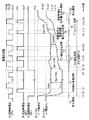
図3は、表示装置1における表示動作の際(駆動回路20による表示駆動の際)の各種波形の一例を、タイミング図で表したものである。ここで、図3(A)〜(C)はそれぞれ、信号線DTL、走査線WSLおよび電源線DSLの電圧波形を示している。具体的には、信号線DTLの電圧が、電圧Vofs、階調補間電圧Vsig1および信号電圧Vsig2の間で周期的に変化している様子(図3(A))と、走査線WSLの電圧が、電圧Voff,Vonの間で周期的に変化している様子(図3(B))と、電源線DSLの電圧が、電圧Vcc,Viniの間で周期的に変化している様子(図3(C))と、をそれぞれ示している。また、図3(D),(E)はそれぞれ、駆動トランジスタTr2におけるゲート電位Vgおよびソース電位Vsの波形を示している。
(2. Details of display operation)
FIG. 3 is a timing chart showing an example of various waveforms during the display operation in the display device 1 (in the display drive by the drive circuit 20). Here, FIGS. 3A to 3C show voltage waveforms of the signal line DTL, the scanning line WSL, and the power supply line DSL, respectively. Specifically, the voltage of the signal line DTL periodically changes among the voltage Vofs, the gradation interpolation voltage Vsig1 and the signal voltage Vsig2 (FIG. 3A), and the voltage of the scanning line WSL The state of periodically changing between the voltages Voff and Von (FIG. 3B) and the state of the voltage of the power supply line DSL periodically changing between the voltages Vcc and Vini (FIG. 3). (C)). 3D and 3E show waveforms of the gate potential Vg and the source potential Vs in the drive transistor Tr2, respectively.
(Vth補正準備期間T1:t1〜t5)
最初に、駆動回路20は、発光期間T0の終了(タイミングt1)後、各画素11(11R,11G,11B)内の駆動トランジスタTr2における閾値電圧Vthの補正(Vth補正)の準備を行う。具体的には、まず、タイミングt1において、電源線駆動回路25が、電源線DSLの電圧を電圧Vccから電圧Viniに下げる(図3(C))。そして、走査線駆動回路23が、信号線DTLの電圧が電圧Vofsとなっており、かつ電源線DSLの電圧が電圧Viniとなっている期間中のタイミングt2〜t3において、走査線WSLの電圧を、電圧Voffから電圧Vonへと上げた状態に設定する(図3(B))。これにより、駆動トランジスタTr2のソース電位Vsが下降して電圧Viniとなり(図3(E))、有機EL素子12が消光する。なお、タイミングt1から、後述する発光動作を開始するタイミングt14までの期間は、有機EL素子12が消光状態である消光期間T10となっている。一方、駆動トランジスタTr2のゲート電位Vgもまた、上記したソース電位Vsの下降に伴い、保持容量素子Csを介した容量カップリングによって下降する(図3(D))。そして、上記したように走査線WSLの電圧が電圧Vonとなり、書き込みトランジスタTr1がオン状態となることにより、駆動トランジスタTr2のゲート電位Vgは、最終的に、このときの信号線DTLの電圧に対応する電圧Vofsとなる(図3(D))。これにより、図3中に示したように、駆動トランジスタTr2におけるゲート−ソース間電圧Vgsが、この駆動トランジスタTr2の閾値電圧Vthよりも大きくなり(Vgs>Vth)、Vth補正の準備が完了する。なお、その後は、信号線DTLの電圧が電圧Vofsとなっており、かつ電源線DSLの電圧が電圧Viniとなっている期間中のタイミングt4において、走査線駆動回路23が、走査線WSLの電圧を、電圧Voffから電圧Vonへと上げる(図3(B))。
(Vth correction preparation period T1: t1 to t5)
First, after the end of the light emission period T0 (timing t1), the
(1回目のVth補正期間T2:t5〜t6)
次に、駆動回路20は、駆動トランジスタTr2における1回目のVth補正を行う。具体的には、まず、信号線DTLの電圧が電圧Vofsとなっており、かつ走査線WSLの電圧が電圧Vonとなっている期間中のタイミングt5において、電源線駆動回路25が電源線DSLの電圧を、電圧Viniから電圧Vccに上げる(図3(C))。すると、駆動トランジスタTr2のドレイン−ソース間に電流Idが流れ、ソース電位Vsが上昇する(図3(E))。次に、信号線DTLおよび電源線DSLの電圧がそれぞれ、電圧Vofs,電圧Vccのまま保持されている期間中のタイミングt6において、走査線駆動回路23が走査線WSLの電圧を、電圧Vonから電圧Voffに下げる(図3(B))。これにより、書き込みトランジスタTr1がオフ状態となるため、駆動トランジスタTr2のゲートがフローティングとなり、Vth補正が一旦停止する(以下の1回目のVth補正休止期間T3へと移行する)。
(First Vth correction period T2: t5 to t6)
Next, the
(1回目のVth補正休止期間T3:t6〜t7)
次に、タイミングt6から後述するタイミングt7までの期間は、上記したように、Vth補正が一旦停止している。ただし、上記した1回目のVth補正が不十分である場合、すなわち、駆動トランジスタTr2におけるゲート−ソース間電圧Vgsが、この駆動トランジスタTr2の閾値電圧Vthと比べて依然として大きい場合(Vgs>Vth)には、以下のようになる。すなわち、このVth補正休止期間T3中においても、Vgs>Vthとなっていることから、駆動トランジスタTr2のドレイン−ソース間に依然として電流Idが流れることになり、ソース電位Vsが上昇し続ける(図3(E))。一方、駆動トランジスタTr2のゲート電位Vgもまた、このようなソース電位Vsの上昇に伴い、保持容量素子Csを介した容量カップリングにより上昇する(図3(D))。
(First Vth correction suspension period T3: t6 to t7)
Next, during the period from timing t6 to timing t7 to be described later, Vth correction is temporarily stopped as described above. However, when the first Vth correction described above is insufficient, that is, when the gate-source voltage Vgs of the drive transistor Tr2 is still higher than the threshold voltage Vth of the drive transistor Tr2 (Vgs> Vth). Is as follows. That is, since Vgs> Vth even during the Vth correction pause period T3, the current Id still flows between the drain and source of the drive transistor Tr2, and the source potential Vs continues to rise (FIG. 3). (E)). On the other hand, the gate potential Vg of the drive transistor Tr2 also rises due to capacitive coupling through the storage capacitor element Cs as the source potential Vs rises (FIG. 3D).
(2回目のVth補正期間T2:t7〜t8)
次に、駆動回路20は、駆動トランジスタTr2におけるVth補正を再び行う(2回目のVth補正を行う)。具体的には、まず、信号線DTLの電圧が電圧Vofsとなっており、かつ電源線DSLの電圧が電圧Vccとなっている期間中のタイミングt7において、走査線駆動回路23が、走査線WSLの電圧を電圧Voffから電圧Vonに上げる(図3(B))。これにより、書き込みトランジスタTr1がオン状態となるため、駆動トランジスタTr2のゲート電位Vgが再び、このときの信号線DTLの電圧に対応する電圧Vofsとなる(図3(D))。このとき、駆動トランジスタTr2のソース電位Vsが、電圧値(Vofs(=Vg)−Vth)よりも低い場合(Vs<(Vg−Vth))、換言すると、ゲート−ソース間電圧Vgsが依然として閾値電圧Vthよりも大きい場合(Vgs>Vth;Vth補正がまだ完了していない場合)には、以下のようになる。すなわち、駆動トランジスタTr2がカットオフするまで(Vgs=Vthになるまで)、1回目のVth補正期間と同様に、この駆動トランジスタTr2のドレイン−ソース間に電流Idが流れることになり、ソース電位Vsが上昇し続ける(図3(E))。ただし、ここでは以下のようにして、Vgs=Vthとなる前に、Vth補正を再び一旦停止させている。すなわち、その後、信号線DTLおよび電源線DSLの電圧がそれぞれ、電圧Vofs,電圧Vccのまま保持されている期間中のタイミングt8において、走査線駆動回路23が走査線WSLの電圧を、電圧Vonから電圧Voffに下げる(図3(B))。これにより、書き込みトランジスタTr1がオフ状態となるため、駆動トランジスタTr2のゲートがフローティングとなり、Vth補正が再び一旦停止する(以下の2回目のVth補正休止期間T3へと移行する)。
(Second Vth correction period T2: t7 to t8)
Next, the
(2回目のVth補正休止期間T3:t8〜t9)
次に、タイミングt8から後述するタイミングt9までの期間は、上記したように、Vth補正が再び一旦停止している。ただし、ここでは、上記したように2回目のVth補正がまだ不十分であることから(Vgs>Vth)、この2回目のVth補正休止期間T3中にも、駆動トランジスタTr2のドレイン−ソース間に依然として電流Idが流れ、ソース電位Vsが上昇し続ける(図3(E))。また、1回目のVth補正休止期間T3中と同様に、駆動トランジスタTr2のゲート電位Vgもまた、保持容量素子Csを介した容量カップリングにより上昇する(図3(D))。
(Second Vth correction suspension period T3: t8 to t9)
Next, during the period from timing t8 to timing t9 described later, the Vth correction is once again stopped as described above. However, since the second Vth correction is still insufficient (Vgs> Vth) as described above, the drain-source region of the drive transistor Tr2 is also used during the second Vth correction pause period T3. The current Id still flows and the source potential Vs continues to rise (FIG. 3E). As in the first Vth correction pause period T3, the gate potential Vg of the drive transistor Tr2 also rises due to capacitive coupling via the storage capacitor element Cs (FIG. 3D).
(3回目のVth補正期間T2および3回目のVth補正休止期間T3:t9〜t11)
次に、駆動回路20は、駆動トランジスタTr2におけるVth補正を再び行う(3回目のVth補正を行う)。具体的には、まず、信号線DTLの電圧が電圧Vofsとなっており、かつ電源線DSLの電圧が電圧Vccとなっている期間中のタイミングt9において、走査線駆動回路23が、走査線WSLの電圧を電圧Voffから電圧Vonに上げる(図3(B))。これにより、書き込みトランジスタTr1がオン状態となるため、駆動トランジスタTr2のゲート電位Vgが再び、このときの信号線DTLの電圧に対応する電圧Vofsとなる(図3(D))。そして、これまでのVth補正期間T2と同様に、駆動トランジスタTr2がカットオフするまで(Vgs=Vthになるまで)、この駆動トランジスタTr2のドレイン−ソース間に電流Idが流れ、ソース電位Vsが上昇する(図3(E))。ここでは、図3中に示したように、この3回目のVth補正期間T2の終了時にVgs=Vthとなり、Vth補正が完了するものとする。すなわち、保持容量素子Csの両端間の電圧が閾値電圧Vthとなるように充電され、その結果、駆動トランジスタTr2におけるゲート−ソース間電圧Vgsが、閾値電圧Vthとなる。その後、信号線DTLおよび電源線DSLの電圧がそれぞれ、電圧Vofs,電圧Vccのまま保持されている期間中のタイミングt10において、走査線駆動回路23が走査線WSLの電圧を、電圧Vonから電圧Voffに下げる(図3(B))。これにより、書き込みトランジスタTr1がオフ状態となるため、駆動トランジスタTr2のゲートがフローティングとなり、その結果、その後の信号線DTLの電圧の大きさによらず、ゲート−ソース間電圧Vgsを閾値電圧Vthのまま保持することができる。なお、このタイミングt10から後述するタイミングt11までの期間は、3回目のVth補正休止期間T3となっている。
(The third Vth correction period T2 and the third Vth correction suspension period T3: t9 to t11)
Next, the
このようにして、Vth補正期間T2およびVth補正休止期間T3を数回ずつ(ここでは、3回ずつ)繰り返してゲート−ソース間電圧Vgsを閾値電圧Vthに設定することにより(Vth補正を行うことにより)、以下のような効果が得られる。すなわち、駆動トランジスタTr2の閾値電圧Vthが画素11(11R,11G,11B)ごとにばらついた場合であっても、有機EL素子12の発光輝度がばらつくのを回避することができる。
In this manner, the gate-source voltage Vgs is set to the threshold voltage Vth by repeating the Vth correction period T2 and the Vth correction pause period T3 several times (here, three times each) (Vth correction is performed). The following effects can be obtained. That is, even when the threshold voltage Vth of the drive transistor Tr2 varies for each pixel 11 (11R, 11G, 11B), it is possible to avoid the variation in the light emission luminance of the
(移動度補正・階調補完書き込み期間T4:t11〜t12)
次に、駆動回路20は、以下説明するようにして、階調補間電圧Vsig1の書き込み(階調補間書き込み)を行いつつ、駆動トランジスタTr2における移動度μの補正(1回目の移動度補正)を行う。具体的には、まず、信号線DTLの電圧が階調補間電圧Vsig1となっており、かつ電源線DSLの電圧が電圧Vccとなっている期間中のタイミングt11において、走査線駆動回路23が、走査線WSLの電圧を電圧Voffから電圧Vonに上げる(図3(B))。これにより、書き込みトランジスタTr1がオン状態となるため、駆動トランジスタTr2のゲート電位Vgが、電圧Vofsから、このときの信号線DTLの電圧に対応する階調補間電圧Vsig1へと上昇する(図3(D))。このとき、有機EL素子12のアノード電圧は、この段階ではまだ、有機EL素子12における閾値電圧Velとカソード電圧Vcaとを足し合わせた電圧値(Vel+Vca)よりも小さいため、有機EL素子12はカットオフ状態となっている。すなわち、この段階ではまだ、有機EL素子12のアノード−カソード間には電流が流れない(有機EL素子12が発光しない)。したがって、駆動トランジスタTr2から供給される電流Idは、有機EL素子12のアノード−カソード間に並列に存在する素子容量(図示せず)へと流れ、この素子容量が充電される。その結果、駆動トランジスタTr2のソース電位Vsが電位差ΔV1だけ上昇し(図3(E))、ゲート−ソース間電圧Vgsが(Vsig1+Vth−ΔV1)となる。
(Mobility correction / tone correction writing period T4: t11 to t12)
Next, as described below, the
このとき、駆動トランジスタTr2の移動度μが大きくなるのに応じて、ソース電位Vsの上昇分(電位差ΔV1)も大きくなる。そのため、上記のように、ゲート−ソース間電圧Vgsが、後述する発光前にこの電位差ΔV1の分だけ小さく設定されることにより(フィードバックがかかることにより)、画素11ごとの移動度μのばらつきを取り除くことができる。ただし、ここでは以下説明するように、このような移動度補正を一旦休止させるため、画素11ごとの移動度μのばらつきは、この段階では完全には取り除かれていないことになる。このようにして、階調補完書き込みと同時に、1回目の移動度補正が行われる。
At this time, as the mobility μ of the drive transistor Tr2 increases, the increase in the source potential Vs (potential difference ΔV1) also increases. Therefore, as described above, the gate-source voltage Vgs is set to be smaller by the potential difference ΔV1 before light emission, which will be described later (by applying feedback), thereby varying the mobility μ for each
(ブートストラップ期間T5:t12〜t13)
次に、信号線DTLおよび電源線DSLの電圧がそれぞれ、階調補間電圧Vsig1,電圧Vccのまま保持されている期間中のタイミングt12において、走査線駆動回路23が、走査線WSLの電圧を電圧Vonから電圧Voffに下げる(図3(B))。これにより、書き込みトランジスタTr1がオフ状態となるため、駆動トランジスタTr2のゲートがフローティングとなり、移動度補正が一旦停止する。また、このとき、駆動トランジスタTr2のソース電位Vsも浮遊電位となっており、かつ、図3中に示したように、ゲート−ソース間電圧Vgsが再び閾値電圧Vthよりも大きくなっている(Vgs>Vth)。このため、駆動トランジスタTr2がブートストラップし、そのソース電位Vsが上昇する(図3(E);ブートストラップ期間T5)。つまり、このブートストラップ期間T5もまた、前述した移動度補正と同様の動作がなされることになる。ただし、ここでは、上記したように駆動トランジスタTr2のゲートがフローティングとなっているため、駆動トランジスタTr2のゲート電位Vgもまた、保持容量素子Csを介した容量カップリングにより上昇している(図3(D))。
(Bootstrap period T5: t12 to t13)
Next, at timing t12 during the period in which the voltages of the signal line DTL and the power supply line DSL are held at the gradation interpolation voltage Vsig1 and the voltage Vcc, the scanning
(移動度補正・信号書き込み期間T6:t13〜t14)
次に、駆動回路20は、以下説明するようにして、信号電圧Vsig2の書き込み(信号書き込み)を行いつつ、2回目の移動度補正を行う。具体的には、まず、信号線DTLの電圧が信号電圧Vsig2となっており、かつ電源線DSLの電圧が電圧Vccとなっている期間中のタイミングt13において、走査線駆動回路23が、走査線WSLの電圧を電圧Voffから電圧Vonに上げる(図3(B))。これにより、書き込みトランジスタTr1がオン状態となるため、駆動トランジスタTr2のゲート電位Vgが、このときの信号線DTLの電圧に対応する信号電圧Vsig2へと上昇する(図3(D))。このとき、有機EL素子12のアノード電圧は、この段階でもまだ、有機EL素子12における閾値電圧Velとカソード電圧Vcaとを足し合わせた電圧値(Vel+Vca)よりも小さく、有機EL素子12は依然としてカットオフ状態となっている。すなわち、この段階でもまだ、有機EL素子12のアノード−カソード間には電流が流れない(有機EL素子12が発光しない)。したがって、駆動トランジスタTr2から供給される電流Idは、前述した有機EL素子12における素子容量(図示せず)へと流れ、この素子容量が充電される。その結果、ここでは、駆動トランジスタTr2のソース電位Vsが電位差ΔV2だけ上昇し(図3(E))、ゲート−ソース間電圧Vgsが、(Vsig2+Vth−(ΔV1+ΔV2))となる。
(Mobility correction / signal writing period T6: t13 to t14)
Next, as described below, the
このとき、駆動トランジスタTr2の移動度μが大きくなるのに応じて、1回目の移動度補正の際と同様に、ソース電位Vsの上昇分(電位差ΔV2)も大きくなる。そのため、上記のように、ゲート−ソース間電圧Vgsが、後述する発光前にこの電位差ΔV2の分だけ更に小さく設定されることにより、画素11ごとの移動度μのばらつきを完全に取り除くことができる。このようにして、信号書き込みと同時に2回目の移動度補正が行われる。
At this time, as the mobility μ of the drive transistor Tr2 increases, the increase in the source potential Vs (potential difference ΔV2) also increases as in the first mobility correction. Therefore, as described above, the gate-source voltage Vgs is set to be smaller by the potential difference ΔV2 before light emission, which will be described later, so that the variation in mobility μ for each
(発光期間T7(T0):t14以降)
次に、信号線DTLおよび電源線DSLの電圧がそれぞれ、階調補間電圧Vsig2,電圧Vccのまま保持されている期間中のタイミングt14において、走査線駆動回路23が、走査線WSLの電圧を電圧Vonから電圧Voffに下げる(図3(B))。これにより、書き込みトランジスタTr1がオフ状態となるため、駆動トランジスタTr2のゲートがフローティングとなる。すると、この駆動トランジスタTr2のゲート−ソース間電圧Vgsが一定に保持された状態で、駆動トランジスタTr2のドレイン−ソース間に電流Idが流れる。その結果、この駆動トランジスタTr2のソース電位Vsが上昇する(図3(E))と共に、駆動トランジスタTr2のゲート電位Vgもまた、保持容量素子Csを介した容量カップリングにより、連動して上昇する(図3(D))。そして、これにより、有機EL素子12のアノード電圧が、この有機EL素子12における閾値電圧Velとカソード電圧Vcaとを足し合わせた電圧値(Vel+Vca)よりも大きくなる。よって、有機EL素子12のアノード−カソード間に電流Idが流れ、有機EL素子12が所望の輝度で発光する(発光期間T7(T0))。
(Light emission period T7 (T0): after t14)
Next, at timing t14 during the period in which the voltages of the signal line DTL and the power supply line DSL are held at the gradation interpolation voltage Vsig2 and the voltage Vcc, the scanning
(繰り返し)
次に、駆動回路20は、所定の期間が経過したのち、発光期間T7(T0)を終了させる。具体的には、前述したのと同様に、タイミングt1において、電源線駆動回路25が、電源線DSLの電圧を電圧Vccから電圧Viniに下げる(図3(C))。すると、駆動トランジスタTr2のソース電位Vsが下降していき、最終的に電圧Viniとなる(図3(E))。このため、有機EL素子12のアノード電圧が、この有機EL素子12における閾値電圧Velとカソード電圧Vcaとを足し合わせた電圧値(Vel+Vca)よりも小さくなり、アノード−カソード間に電流Idが流れなくなる。その結果、このタイミングt1以降、有機EL素子12が消光する(前述した消光期間T10へと移行する)。なお、その後は、駆動回路20は、これまで説明した各期間T1〜T7(T0)がフレーム期間ごとに周期的に繰り返されるように、表示駆動を行う。また、それと共に、駆動回路20は、例えば1水平期間(1H期間)ごとに、電源線DSLに印加する選択パルスおよび走査線WSLに印加する制御パルスをそれぞれ、行方向に走査させる。以上のようにして、表示装置1における表示動作(駆動回路20による表示駆動)がなされる。
(repetition)
Next, the
(3.階調補間動作)
続いて、本実施の形態の表示装置1における表示動作の際の特徴的部分の1つである、駆動回路20による階調補間動作(各有機EL素子12における発光輝度の階調を補間する動作)について、比較例の表示動作と比較しつつ詳細に説明する。
(3. Gradation interpolation operation)
Subsequently, a gradation interpolation operation by the drive circuit 20 (an operation for interpolating the gradation of light emission luminance in each organic EL element 12), which is one of the characteristic parts in the display operation in the
(3−1.比較例の表示動作)
図4は、比較例に係る従来の表示装置における表示動作の際の各種波形の一例を、タイミング図で表したものである(タイミングt101〜t112)。ここで、図4(A)〜(C)はそれぞれ、前述した図3(A)〜(C)と同様に、信号線DTL、走査線WSLおよび電源線DSLの電圧波形を示している。ただし、ここでは図4(A)については、図3(A)とは異なり、信号線DTLの電圧が、電圧Vofsおよび信号電圧Vsig(2値の電圧)の間で周期的に変化している様子を示している。また、図4(D),(E)はそれぞれ、前述した図3(D),(E)と同様に、駆動トランジスタTr2におけるゲート電位Vgおよびソース電位Vsの波形を示している。
(3-1. Display operation of comparative example)
FIG. 4 is a timing chart showing an example of various waveforms during the display operation in the conventional display device according to the comparative example (timing t101 to t112). Here, FIGS. 4A to 4C show voltage waveforms of the signal line DTL, the scanning line WSL, and the power supply line DSL, respectively, similarly to FIGS. 3A to 3C described above. However, in FIG. 4A, unlike FIG. 3A, the voltage of the signal line DTL periodically changes between the voltage Vofs and the signal voltage Vsig (binary voltage). It shows a state. Further, FIG. 4 (D), the shows (E), respectively, FIG. 3 described above (D), in the same manner as (E), the waveform of the gate potential Vg and the source potential Vs of the drive transistor Tr2.
この比較例の表示動作は、タイミングt101〜t111の期間(Vth補正準備期間T1、1〜3回目のVth補正期間T2および1〜3回目のVth補正休止期間)の動作については、表示装置1の表示動作(図3中のタイミングt1〜t11の期間の動作)と、基本的に同様である。すなわち、上記したように、信号線DTLの電圧が2値(電圧Vofsおよび信号電圧Vsig)となっていることを除き、表示装置1と同様のVth補正動作がなされている。
The display operation of this comparative example is the operation of the
一方、比較例の表示動作のうち、タイミングt111〜t112の期間(移動度補正・信号書き込み期間T8)の動作については、表示装置1におけるタイミングt11〜t14の期間の動作とは異なっている。すなわち、比較例では、以下説明する表示装置1の動作とは異なり、移動度補正・信号書き込み期間T8の1回のみで、信号書き込みおよび移動度補正を行っている。具体的には、外部から入力される映像信号20Aに対応する信号電圧Vsigの書き込み動作と、これまで説明したのと同様の移動度補正(ここでは、ソース電位Vsを電位差ΔVだけ上昇させている)とを行っている。なお、タイミングt112以降の発光期間T9(T0)の動作については、表示装置1における発光期間T7(T0)の動作と基本的に同様である。
On the other hand, in the display operation of the comparative example, the operation in the period from timing t111 to t112 (mobility correction / signal writing period T8) is different from the operation in the period from timing t11 to t14 in the
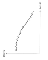
このとき、この比較例の表示動作では、信号電圧Vsigと、駆動トランジスタTr2に流れる電流Id(有機EL素子12の発光輝度Lに比例)との関係(ガンマカーブ)は、例えば図5(A)に示したようになる。すなわち、映像信号20Aにより設定される信号電圧Vsigの階調が、例えば電圧x,x+1,x+2,…と増加するのに応じて、電流Id(発光輝度L)の階調も、1対1の関係で増加している。具体的には、信号電圧Vsigが電圧xに設定されているとき、電流Idは電流値Id(x),発光輝度Lは輝度L(x)となっている。同様に、信号電圧Vsigが電圧(x+1)に設定されているとき、電流Idは電流値Id(x+1),発光輝度Lは輝度L(x+1)となり、信号電圧Vsigが電圧(x+2)に設定されているとき、電流Idは電流値Id(x+2),発光輝度Lは輝度L(x+2)となる。このことから、比較例の表示動作を用いた場合、映像信号20Aにより設定可能な階調数(映像信号20Aのビット数)、言い換えると、信号電圧Vsigにおいて設定可能な電圧値の数によって、一義的に発光輝度Lの階調数が定まることになる。具体的には、例えば映像信号20Aが8ビットの信号である場合、表現可能な発光輝度Lの階調数は、28=256となる。また、例えば映像信号20Aが10ビットの信号である場合、表現可能な発光輝度Lの階調数は、210=1024となる。 At this time, in the display operation of this comparative example, the relationship (gamma curve) between the signal voltage Vsig and the current Id flowing through the drive transistor Tr2 (proportional to the light emission luminance L of the organic EL element 12) is, for example, FIG. As shown in That is, as the gradation of the signal voltage Vsig set by the video signal 20A increases, for example, to voltages x, x + 1, x + 2,..., The gradation of the current Id (light emission luminance L) is also 1: 1. The relationship has increased. Specifically, when the signal voltage Vsig is set to the voltage x, the current Id is the current value Id (x), and the light emission luminance L is the luminance L (x). Similarly, when the signal voltage Vsig is set to the voltage (x + 1), the current Id is set to the current value Id (x + 1), the light emission luminance L is set to the luminance L (x + 1), and the signal voltage Vsig is set to the voltage (x + 2). The current Id is the current value Id (x + 2), and the light emission luminance L is the luminance L (x + 2). Therefore, when the display operation of the comparative example is used, the number of gradations that can be set by the video signal 20A (the number of bits of the video signal 20A), that is, the number of voltage values that can be set in the signal voltage Vsig is unambiguous. Therefore, the number of gradations of the light emission luminance L is determined. Specifically, for example, when the video signal 20A is an 8-bit signal, the number of gradations of the light emission luminance L that can be expressed is 2 8 = 256. For example, when the video signal 20A is a 10-bit signal, the number of gradations of the light emission luminance L that can be expressed is 2 10 = 1024.
したがって、表示装置全体としての低コスト化を実現するための手法の1つとして、例えばデータドライバ(信号線駆動回路24に相当)のコスト削減を図る場合、比較例の表示動作を用いた表示装置では、以下の問題が生ずる。すなわち、例えば、映像信号20Aにより設定可能な階調数(映像信号20Aのビット数)を削減して、このデータドライバのコスト削減を図ることが考えられるが、この比較例の表示動作を用いた場合、それに伴い、表現可能な発光輝度Lの階調数も減少してしまう。具体的には、現在のところ一般的となっている10ビット階調(1024階調)に対し、低コスト化を実現するためには、例えば8ビット階調(256階調)などに階調数を間引かなければならないことになる。このように、表現可能な発光輝度Lの階調数が減少すると、それに伴って表示画質も低下してしまうことから、比較例の表示動作を用いた場合、低コスト化を図りつつ高画質化を実現する(低コスト化と高画質化との両立)のが困難である。 Accordingly, as one of the methods for reducing the cost of the entire display device, for example, when reducing the cost of a data driver (corresponding to the signal line drive circuit 24), a display device using the display operation of the comparative example Then, the following problems arise. That is, for example, the number of gradations (number of bits of the video signal 20A) that can be set by the video signal 20A can be reduced to reduce the cost of the data driver, but the display operation of this comparative example was used. In this case, the number of gradations of the light emission luminance L that can be expressed also decreases. Specifically, in order to realize a reduction in cost with respect to the 10-bit gradation (1024 gradation) that is generally used at present, the gradation is reduced to, for example, an 8-bit gradation (256 gradations). You will have to thin out the numbers. Thus, if the number of gradations of the light emission luminance L that can be expressed decreases, the display image quality also decreases accordingly. Therefore, when the display operation of the comparative example is used, the image quality is improved while reducing the cost. It is difficult to realize (a balance between low cost and high image quality).
(3−2.実施の形態における階調補間動作)
これに対して、本実施の形態の表示装置1では、まず、上記比較例とは異なり、信号書き込みの2ステップ化が図られている。具体的には、図3に示したように、タイミングt11〜t14の期間において、ブートストラップ期間T5を挟んで2回の移動度補正・信号書き込み期間(移動度補正・階調補間書き込み期間T4および移動度補正・信号書き込み期間T6)が設けられている。また、信号線駆動回路24は、映像信号20Aに基づく信号電圧である階調補間電圧Vsig1および信号電圧Vsig2と、電圧Vofsとの3つの電圧(3値の電圧)を出力することが可能となっている。そして、この信号線駆動回路24は、これら2つの信号電圧を、図3に示したように、階調補完電圧Vsig1および信号電圧Vsig2の順に各信号線DTLに対して印加すると共に、以下説明するように、階調補完電圧Vsig1および信号電圧Vsig2の電圧値を個別に変化させている。
(3-2. Gradation Interpolation Operation in Embodiment)
On the other hand, in the
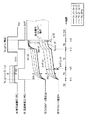
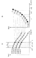
これにより、表示装置1では、例えば図5(B)中の符号P11,P12で示したように、各有機EL素子12における発光輝度Lの階調を補間する階調補間動作を行っている。その結果、この表示装置1では、映像信号20Aによって元々設定することが可能な階調数よりも多くの階調の表現が実現される。具体的には、例えば図5(A)に示した信号電圧Vsigにおいて設定される電圧x等が8ビット階調である場合、図5(B)では、この8ビット階調に対して2ビット分の階調(4階調)が補間されるため(符号P11,P12参照)、10ビット階調が実現される。すなわち、信号電圧Vsig2において設定される電圧x等(基本階調電圧)に対し、以下詳述するように、階調補間電圧Vsig1において設定される電圧y等(補間階調電圧)を用いることで2ビット分の階調(4階調)が補間され、合計10ビット階調となる。
Thereby, in the
ここで、このような階調補間動作についてより具体的に説明すると、以下のようになる。すなわち、まず、信号線駆動回路24は、例えば図6(A)〜(D)に示したように、信号電圧Vsig2を、映像信号20Aにより設定可能な複数の階調(ここでは、8ビット階調=256階調)のうちの一の階調に対応する電圧(ここでは、電圧x)に固定して設定する。次いで、例えば図6(A)中の矢印P21で示したように、信号線駆動回路24は、階調補間電圧Vsig1を複数の電圧(ここでは、電圧(y−3),(y−2),(y−1),yの4つの電圧)間で変化させる。そして、信号線駆動回路24は、信号電圧Vsig2を、上記した複数の階調のうちの他の階調に固定して設定すると共に、階調補間電圧Vsig1を、再び上記した複数の電圧間で変化させる、という動作を繰り返す。
Here, the gradation interpolation operation will be described more specifically as follows. That is, first, as shown in FIGS. 6A to 6D, for example, the signal
このとき、図6(A),(D)中の矢印P21,P22で示したように、階調補間電圧Vsig1の電圧値が電圧(y−3)から電圧yへと上昇するのに応じて、この階調補間電圧Vsig1の書き込み後における駆動トランジスタTr2のソース電位Vsの上昇も大きくなる。具体的には、例えば、階調補間電圧Vsig1が電圧(y−3)に設定されているときのソース電位Vsの上昇分(1回目の移動度補正による電位差ΔV1(y−3))よりも、階調補間電圧Vsig1が電圧yに設定されているときのソース電位Vsの上昇分(電位差ΔV1(y))のほうが、大きくなっている。また、このとき、この移動度補正・階調補間書き込み期間T4では、図6(C)中の矢印P23で示したように、このような駆動トランジスタTr2のソース電位Vsの上昇に伴って、駆動トランジスタTr2のゲート電位Vgも連動して上昇する。すなわち、階調補間電圧Vsig1の電圧値が電圧(y−3)から電圧yへと上昇するのに応じて、この階調補間電圧Vsig1の書き込み後におけるゲート電位Vgの上昇も大きくなる。 At this time, as indicated by arrows P21 and P22 in FIGS. 6A and 6D, the voltage value of the gradation interpolation voltage Vsig1 rises from the voltage (y-3) to the voltage y. The increase in the source potential Vs of the drive transistor Tr2 after the writing of the gradation interpolation voltage Vsig1 also increases. Specifically, for example, the amount of increase of the source potential Vs when the gradation interpolation voltage Vsig1 is set to the voltage (y-3) (potential difference ΔV1 (y-3) by the first mobility correction). The increase in the source potential Vs (potential difference ΔV1 (y)) when the gradation interpolation voltage Vsig1 is set to the voltage y is larger. At this time, in the mobility correction / gradation interpolation writing period T4, as indicated by an arrow P23 in FIG. 6C, the driving is performed as the source potential Vs of the driving transistor Tr2 increases. The gate potential Vg of the transistor Tr2 also rises in conjunction with it. That is, as the voltage value of the gradation interpolation voltage Vsig1 increases from the voltage (y-3) to the voltage y, the increase in the gate potential Vg after the gradation interpolation voltage Vsig1 is written increases.
一方、移動度補正・信号書き込み期間T6では、駆動トランジスタTr2のソース電位Vsの上昇分(2回目の移動度補正による電位差ΔV2)は、図6(D)に示したように、階調補間電圧Vsig1の電圧値によらず、一定となっている。これは、前述したように、この期間でのソース電位Vsの上昇分(電位差ΔV2)は、この際に書き込まれる信号電圧Vsig2の電圧値(ここでは、電圧x)により定まるからである。また、この期間終了後には、やはり前述したように、駆動トランジスタTr2のゲート電位Vgは、信号電圧Vsig2(ここでは、電圧x)となる(図6(C))。これらのことから、図6から分かるように、階調補間電圧Vsig1の電圧値が電圧(y−3)から電圧yへと上昇するのに応じて、信号電圧Vsig2の書き込み後(発光動作時)における駆動トランジスタTr2のゲート−ソース間電圧Vgsは小さくなる。具体的には、例えば、階調補間電圧Vsig1が電圧(y−3)に設定されているときのゲート−ソース間電圧Vgs(y−3))よりも、階調補間電圧Vsig1が電圧yに設定されているときのゲート−ソース間電圧Vgs(y))のほうが、小さくなっている。 On the other hand, in the mobility correction / signal writing period T6, the increase in the source potential Vs of the drive transistor Tr2 (the potential difference ΔV2 due to the second mobility correction) is, as shown in FIG. It is constant regardless of the voltage value of Vsig1. This is because, as described above, the increase in the source potential Vs during this period (potential difference ΔV2) is determined by the voltage value (here, voltage x) of the signal voltage Vsig2 written at this time. Further, after the end of this period, as described above, the gate potential Vg of the drive transistor Tr2 becomes the signal voltage Vsig2 (here, the voltage x) (FIG. 6C). From these facts, as can be seen from FIG. 6, after the signal voltage Vsig2 is written (during the light emission operation), the voltage value of the gradation interpolation voltage Vsig1 rises from the voltage (y-3) to the voltage y. The gate-source voltage Vgs of the drive transistor Tr2 in FIG. Specifically, for example, the grayscale interpolation voltage Vsig1 is set to the voltage y rather than the gate-source voltage Vgs (y-3) when the grayscale interpolation voltage Vsig1 is set to the voltage (y-3). The gate-source voltage Vgs (y)) when set is smaller.
これにより、例えば図7に示したように、階調補間電圧Vsig1の電圧値が上昇するのに応じて、発光動作時における駆動トランジスタTr2のゲート−ソース間電圧Vgsが小さくなる結果、この駆動トランジスタTr2を流れる電流Idが減少する。また、この電流Idが減少するのに比例して、有機EL素子12の発光輝度Lも低くなる。
As a result, for example, as shown in FIG. 7, as the voltage value of the gradation interpolation voltage Vsig1 increases, the gate-source voltage Vgs of the drive transistor Tr2 during the light emission operation decreases. As a result, the drive transistor The current Id flowing through Tr2 decreases. In addition, the light emission luminance L of the
これを利用して、信号線駆動回路24は、例えば図8に示したように、信号電圧Vsig2により設定可能な階調に対応する電圧x等のそれぞれに対し(図8(B))、階調補間電圧Vsig1により設定される4つ階調に対応する電圧y等(図8(A))を選択して割り当てる。これにより、図5(B),図8(B)に示したような階調補間動作が実現される。なお、図8(A)中の電圧範囲Δyは、階調補間電圧Vsig1により設定される4つ階調の階調区間を示している。
By utilizing this, the signal
以上のように本実施の形態では、表示パネル10内の複数の画素11に対する表示駆動の際に、駆動回路20(信号線駆動回路24)が、映像信号20Aの階調に応じて階調補間電圧Vsig1および信号電圧Vsig2の電圧値を個別に変化させることにより、各有機EL素子12における発光輝度Lの階調を補間する階調補間動作を行うようにしたので、映像信号20Aによって元々設定することが可能な階調数よりも多くの階調の表現を実現することができる。よって、駆動回路20(信号線駆動回路24)の構成を簡素化しつつ(複雑化することなく)、より高精細な階調表現が実現される。すなわち、例えばM(M:整数)ビットの映像信号20Aを出力可能なデータドライバ(信号線駆動回路24)を用いた場合であっても、N(N:整数,N>M)ビットの階調表現が可能となり、駆動回路20のコスト削減を図ることができる。以上のことから、本実施の形態の表示装置1によれば、低コスト化を図りつつ高画質化を実現する(低コスト化と高画質化とを両立させる)ことが可能となる。
As described above, in the present embodiment, when display driving is performed on the plurality of
<モジュールおよび適用例>
続いて、図9〜図14を参照して、上記実施の形態で説明した表示装置1の適用例について説明する。上記実施の形態の表示装置1は、テレビジョン装置,デジタルカメラ,ノート型パーソナルコンピュータ、携帯電話等の携帯端末装置あるいはビデオカメラなどのあらゆる分野の電子機器に適用することが可能である。言い換えると、この表示装置1は、外部から入力された映像信号あるいは内部で生成した映像信号を、画像あるいは映像として表示するあらゆる分野の電子機器に適用することが可能である。
<Modules and application examples>
Subsequently, an application example of the
(モジュール)
表示装置1は、例えば、図9に示したようなモジュールとして、後述する適用例1〜5などの種々の電子機器に組み込まれる。このモジュールは、例えば、基板31の一辺に、封止用基板32から露出した領域210を設け、この露出した領域210に、駆動回路20の配線を延長して外部接続端子(図示せず)を形成したものである。この外部接続端子には、信号の入出力のためのフレキシブルプリント配線基板(FPC;Flexible Printed Circuit)220が設けられていてもよい。
(module)
The
(適用例1)
図10は、表示装置1が適用されるテレビジョン装置の外観を表したものである。このテレビジョン装置は、例えば、フロントパネル310およびフィルターガラス320を含む映像表示画面部300を有しており、この映像表示画面部300が表示装置1により構成されている。
(Application example 1)
FIG. 10 illustrates an appearance of a television device to which the
(適用例2)
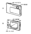
図11は、表示装置1が適用されるデジタルカメラの外観を表したものである。このデジタルカメラは、例えば、フラッシュ用の発光部410、表示部420、メニュースイッチ430およびシャッターボタン440を有しており、この表示部420が表示装置1により構成されている。
(Application example 2)
FIG. 11 shows the appearance of a digital camera to which the
(適用例3)
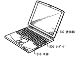
図12は、表示装置1が適用されるノート型パーソナルコンピュータの外観を表したものである。このノート型パーソナルコンピュータは、例えば、本体510,文字等の入力操作のためのキーボード520および画像を表示する表示部530を有しており、この表示部530が表示装置1により構成されている。
(Application example 3)
FIG. 12 shows the appearance of a notebook personal computer to which the
(適用例4)
図13は、表示装置1が適用されるビデオカメラの外観を表したものである。このビデオカメラは、例えば、本体部610,この本体部610の前方側面に設けられた被写体撮影用のレンズ620,撮影時のスタート/ストップスイッチ630および表示部640を有している。そして、この表示部640が表示装置1により構成されている。
(Application example 4)
FIG. 13 shows the appearance of a video camera to which the
(適用例5)
図14は、表示装置1が適用される携帯電話機の外観を表したものである。この携帯電話機は、例えば、上側筐体710と下側筐体720とを連結部(ヒンジ部)730で連結したものであり、ディスプレイ740,サブディスプレイ750,ピクチャーライト760およびカメラ770を有している。そして、これらのうちのディスプレイ740またはサブディスプレイ750が、表示装置1により構成されている。
(Application example 5)
FIG. 14 shows the appearance of a mobile phone to which the
<変形例>
以上、実施の形態および適用例を挙げて本発明を説明したが、本発明はこれらの実施の形態等に限定されず、種々の変形が可能である。
<Modification>
While the present invention has been described with reference to the embodiments and application examples, the present invention is not limited to these embodiments and the like, and various modifications are possible.
例えば、上記実施の形態等では、主に、階調補間動作によって、映像信号20Aにより設定可能な8ビット階調から2ビット分補間することにより、発光輝度Lにおいて10ビット階調を表現可能とする場合について説明したが、この場合には限られない。すなわち、上記実施の形態等で説明した階調補間動作を用いることにより、例えば、6ビット階調から4ビット分補間して10ビット階調の表現を実現したり、10ビット階調から2ビット分補間して12ビット階調の表現を実現したりすることも可能である。ただし、元々Mビット階調に設定された映像信号に対し、Nビット分補間する場合には、階調補間電圧Vsig1を2N値間で変化させるようにすればよい。 For example, in the above-described embodiment, a 10-bit gradation can be expressed in the light emission luminance L by interpolating 2 bits from the 8-bit gradation that can be set by the video signal 20A mainly by the gradation interpolation operation. However, the present invention is not limited to this case. In other words, by using the gradation interpolation operation described in the above embodiments, for example, 10-bit gradation can be expressed by interpolating 4 bits from 6-bit gradation, or from 10-bit gradation to 2-bit. It is also possible to realize 12-bit gradation expression by partial interpolation. However, when N-bit interpolation is performed on a video signal originally set to M-bit gradation, the gradation interpolation voltage Vsig1 may be changed between 2 N values.
また、上記実施の形態等では、表示装置1がアクティブマトリクス型である場合について説明したが、アクティブマトリクス駆動のための画素回路14の構成は、上記実施の形態等で説明したものに限られない。すなわち、必要に応じて容量素子やトランジスタ等を画素回路14に追加するようにしてもよい。その場合、画素回路14の変更に応じて、上述した走査線駆動回路23、信号線駆動回路24および電源線駆動回路25の他に、必要な駆動回路を追加するようにしてもよい。
In the above-described embodiment and the like, the case where the
更に、上記実施の形態等では、走査線駆動回路23、信号線駆動回路24および電源線駆動回路25における駆動動作を、タイミング生成回路22が制御する場合について説明したが、他の回路がこれらの駆動動作を制御するようにしてもよい。また、このような走査線駆動回路23、信号線駆動回路24および電源線駆動回路25に対する制御は、ハードウェア(回路)で行われるようにしてもよいし、ソフトウェア(プログラム)で行われるようにしてもよい。
Further, in the above-described embodiment and the like, the case where the
加えて、上記実施の形態等では、画素回路14がいわゆる「2Tr1C」の回路構成となっている場合について説明したが、画素回路14の回路構成はこれには限られない。すなわち、トランジスタが有機EL素子12に直列に接続された回路構成を含んでいるものであれば、画素回路14が「2Tr1C」以外の回路構成となっていてもよい。
In addition, in the above-described embodiment and the like, the case where the pixel circuit 14 has a so-called “2Tr1C” circuit configuration has been described, but the circuit configuration of the pixel circuit 14 is not limited thereto. That is, as long as the transistor includes a circuit configuration connected in series to the
また、上記実施の形態等では、書き込みトランジスタTr1および駆動トランジスタTr2がそれぞれ、nチャネルトランジスタ(例えば、nチャネルMOS型のTFT)により形成されている場合について説明したが、この場合には限られない。すなわち、書き込みトランジスタTr1および駆動トランジスタTr2がそれぞれ、pチャネルトランジスタ(例えば、pチャネルMOS型のTFT)により形成されていてもよい。ただし、その場合には、駆動トランジスタTr2におけるソースおよびドレインのうちの電源線DSLに接続されていない方と、保持容量素子Csの他端とを、有機EL素子12のカソードに接続し、有機EL素子12のアノードをグランド線GND等に接続することが好ましい。
In the above-described embodiment and the like, the case where the write transistor Tr1 and the drive transistor Tr2 are each formed by an n-channel transistor (for example, an n-channel MOS type TFT) has been described. However, the present invention is not limited to this case. . That is, each of the write transistor Tr1 and the drive transistor Tr2 may be formed of a p-channel transistor (for example, a p-channel MOS type TFT). However, in that case, one of the source and drain of the drive transistor Tr2 that is not connected to the power supply line DSL and the other end of the storage capacitor element Cs are connected to the cathode of the
1…表示装置、10…表示パネル、11,11R,11G,11B…画素、12R,12G,12B…有機EL素子、13…画素アレイ部、14…画素回路、20…駆動回路、20A,21A…映像信号、20B…同期信号、21…映像信号処理回路、22…タイミング生成回路、22A…制御信号、23…走査線駆動回路、24…信号線駆動回路、25…電源線駆動回路、WSL…走査線、DTL…信号線、DSL…電源線、Tr1…書き込みトランジスタ、Tr2…駆動トランジスタ、Cs…保持容量素子、Id…電流、Vg…ゲート電位、Vs…ソース電位、Vgs…ゲート−ソース間電圧、Vth…閾値電圧、Vsig1…階調補間電圧、Vsig2…信号電圧、Vofs,Von,Voff,Vcc,Vini,x,x+1,x+2,y−3,y−2,y−1,y…電圧、ΔV1,ΔV2…電位差、Δy…電圧範囲(階調区間)、L…発光輝度、t1〜t14…タイミング、T0,T7…発光期間、T1…Vth補正準備期間、T2…Vth補正期間、T3…Vth補正休止期間、T4…移動度補正・階調補間書き込み期間、T5…ブートストラップ期間、T6…移動度補正・信号書き込み期間。
DESCRIPTION OF
Claims (7)
前記複数の画素を順次選択しつつ、選択された画素に対して映像信号に基づく第1および第2の信号電圧をこの順に書き込むことにより、前記複数の画素に対する表示駆動を行う駆動回路と
を備え、
前記駆動回路は、
前記駆動トランジスタの閾値電圧補正を複数回繰り返して行い、
前記複数回の前記閾値電圧補正を行った後に、
前記第1の信号電圧を複数の補間階調電圧間で変化させることにより、前記発光素子における発光輝度の階調を補間する階調補間動作を行うと共に、
前記第2の信号電圧を、前記映像信号により設定可能な複数の階調のうちの一の階調に対応する一の基本階調電圧に固定して設定する
表示装置。 A display unit including a plurality of pixels each having a pixel circuit including a light emitting element and a writing transistor and the driving transistor,
A driving circuit that performs display driving for the plurality of pixels by sequentially selecting the plurality of pixels and writing the first and second signal voltages based on the video signal in this order to the selected pixels. ,
The drive circuit is
The threshold voltage correction of the driving transistor is repeated a plurality of times,
After performing the threshold voltage correction a plurality of times,
While changing the first signal voltage between a plurality of interpolation gradation voltages, performing a gradation interpolation operation for interpolating the gradation of light emission luminance in the light emitting element,
A display device that fixes and sets the second signal voltage to one basic gradation voltage corresponding to one gradation among a plurality of gradations that can be set by the video signal .
前記第1および第2の信号電圧の書き込みを行いつつ、前記駆動トランジスタの移動度補正を行うと共に、While performing the writing of the first and second signal voltages, performing mobility correction of the driving transistor,
前記第1の信号電圧の書き込みおよび前記移動度補正の期間と、前記第2の信号電圧の書き込みおよび前記移動度補正の期間との間で、前記駆動トランジスタをブートストラップさせるThe drive transistor is bootstrapped between the period of writing the first signal voltage and the mobility correction period and the period of writing the second signal voltage and the mobility correction period.
請求項1に記載の表示装置。The display device according to claim 1.
請求項1または請求項2に記載の表示装置。 The display device according to claim 1, wherein the display unit includes a plurality of scanning lines, a plurality of signal lines, and a plurality of power supply lines.
前記複数の走査線の各々に対して選択パルスを順次印加することにより、前記複数の画素から1ライン分ずつの画素を順次選択する走査線駆動回路と、
前記第1および第2の信号電圧をこの順に前記複数の信号線の各々に対して印加することにより、前記走査線駆動回路により選択された画素に対して映像信号の書き込みを行う信号線駆動回路と、
前記複数の電源線の各々に対して制御パルスを順次印加することにより、各発光素子の発光動作および消光動作の制御を行う電源線駆動回路とを有する
請求項3に記載の表示装置。 The drive circuit is
A scanning line driving circuit that sequentially selects pixels for one line from the plurality of pixels by sequentially applying a selection pulse to each of the plurality of scanning lines;
A signal line driving circuit for writing video signals to the pixels selected by the scanning line driving circuit by applying the first and second signal voltages to each of the plurality of signal lines in this order. When,
The display device according to claim 3, further comprising: a power line driving circuit that controls a light emitting operation and a quenching operation of each light emitting element by sequentially applying a control pulse to each of the plurality of power lines.
前記画素回路は、ゲート、ソースおよびドレインをそれぞれ有する、前記書き込みトランジスタとしての第1のトランジスタおよび前記駆動トランジスタとしての第2のトランジスタと、保持容量素子とを有し、
前記第1のトランジスタのゲートが、前記走査線に接続され、
前記第1のトランジスタにおけるドレインおよびソースのうち、一方が、前記信号線に接続されると共に、他方が、前記第2のトランジスタのゲートおよび前記保持容量素子の一端に接続され、
前記第2のトランジスタにおけるドレインおよびソースのうち、一方が、前記電源線に接続されると共に、他方が、前記保持容量素子の他端および前記発光素子のアノードに接続され、
前記発光素子のカソードが、固定電位に設定されている
請求項3または請求項4に記載の表示装置。 The light emitting device has an anode and a cathode,
The pixel circuit includes a first transistor as the writing transistor and a second transistor as the driving transistor , each having a gate, a source, and a drain, and a storage capacitor element.
A gate of the first transistor is connected to the scan line;
One of the drain and the source in the first transistor is connected to the signal line, and the other is connected to the gate of the second transistor and one end of the storage capacitor.
One of the drain and the source in the second transistor is connected to the power line, and the other is connected to the other end of the storage capacitor element and the anode of the light emitting element.
The display device according to claim 3, wherein a cathode of the light emitting element is set to a fixed potential.
この表示駆動の際に、
前記駆動トランジスタの閾値電圧補正を複数回繰り返して行い、
前記複数回の前記閾値電圧補正を行った後に、
前記第1の信号電圧を複数の補間階調電圧間で変化させることにより、前記発光素子における発光輝度の階調を補間する階調補間動作を行うと共に、
前記第2の信号電圧を、前記映像信号により設定可能な複数の階調のうちの一の階調に対応する一の基本階調電圧に固定して設定する
表示装置の駆動方法。 For each pixel in the display section, each including a plurality of pixels having a pixel circuit including a light emitting element and a writing transistor and the driving transistor, while sequentially selecting the plurality of pixels, the video signal for the selected pixel The display driving is performed by writing the first and second signal voltages based on the first and second signal voltages in this order, and
During this display drive,
The threshold voltage correction of the driving transistor is repeated a plurality of times,
After performing the threshold voltage correction a plurality of times,
While changing the first signal voltage between a plurality of interpolation gradation voltages, performing a gradation interpolation operation for interpolating the gradation of light emission luminance in the light emitting element,
A method of driving a display device, wherein the second signal voltage is fixedly set to one basic gradation voltage corresponding to one gradation among a plurality of gradations that can be set by the video signal .
前記表示装置は、
各々が発光素子と書き込みトランジスタおよび駆動トランジスタを含む画素回路とを有する複数の画素を含む表示部と、
前記複数の画素を順次選択しつつ、選択された画素に対して映像信号に基づく第1および第2の信号電圧をこの順に書き込むことにより、前記複数の画素に対する表示駆動を行う駆動回路と
を有し、
前記駆動回路は、
前記駆動トランジスタの閾値電圧補正を複数回繰り返して行い、
前記複数回の前記閾値電圧補正を行った後に、
前記第1の信号電圧を複数の補間階調電圧間で変化させることにより、前記発光素子における発光輝度の階調を補間する階調補間動作を行うと共に、
前記第2の信号電圧を、前記映像信号により設定可能な複数の階調のうちの一の階調に対応する一の基本階調電圧に固定して設定する
電子機器。 A display device,
The display device
A display unit including a plurality of pixels each having a pixel circuit including a light emitting element and a writing transistor and the driving transistor,
A drive circuit that performs display driving for the plurality of pixels by sequentially selecting the plurality of pixels and writing first and second signal voltages based on a video signal in this order to the selected pixels; And
The drive circuit is
The threshold voltage correction of the driving transistor is repeated a plurality of times,
After performing the threshold voltage correction a plurality of times,
While changing the first signal voltage between a plurality of interpolation gradation voltages, performing a gradation interpolation operation for interpolating the gradation of light emission luminance in the light emitting element,
An electronic apparatus that fixes and sets the second signal voltage to one basic gradation voltage corresponding to one gradation among a plurality of gradations that can be set by the video signal .
Priority Applications (3)
| Application Number | Priority Date | Filing Date | Title |
|---|---|---|---|
| JP2009258314A JP5493741B2 (en) | 2009-11-11 | 2009-11-11 | Display device, driving method thereof, and electronic apparatus |
| US12/923,764 US8847999B2 (en) | 2009-11-11 | 2010-10-07 | Display device, method for driving the same, and electronic unit |
| CN201010537527XA CN102063863A (en) | 2009-11-11 | 2010-11-04 | Display device, method for driving the same, and electronic unit |
Applications Claiming Priority (1)
| Application Number | Priority Date | Filing Date | Title |
|---|---|---|---|
| JP2009258314A JP5493741B2 (en) | 2009-11-11 | 2009-11-11 | Display device, driving method thereof, and electronic apparatus |
Publications (3)
| Publication Number | Publication Date |
|---|---|
| JP2011102928A JP2011102928A (en) | 2011-05-26 |
| JP2011102928A5 JP2011102928A5 (en) | 2012-11-08 |
| JP5493741B2 true JP5493741B2 (en) | 2014-05-14 |
Family
ID=43973851
Family Applications (1)
| Application Number | Title | Priority Date | Filing Date |
|---|---|---|---|
| JP2009258314A Expired - Fee Related JP5493741B2 (en) | 2009-11-11 | 2009-11-11 | Display device, driving method thereof, and electronic apparatus |
Country Status (3)
| Country | Link |
|---|---|
| US (1) | US8847999B2 (en) |
| JP (1) | JP5493741B2 (en) |
| CN (1) | CN102063863A (en) |
Families Citing this family (8)
| Publication number | Priority date | Publication date | Assignee | Title |
|---|---|---|---|---|
| JP5716292B2 (en) * | 2010-05-07 | 2015-05-13 | ソニー株式会社 | Display device, electronic device, and driving method of display device |
| WO2012033410A2 (en) * | 2010-09-10 | 2012-03-15 | Eldolab Holding B.V. | Led driver circuit and method |
| US9454932B2 (en) * | 2011-11-24 | 2016-09-27 | Joled Inc. | Display device and method of controlling the same |
| JP6111531B2 (en) | 2012-04-25 | 2017-04-12 | セイコーエプソン株式会社 | Electro-optical device, driving method of electro-optical device, and electronic apparatus |
| JP6201465B2 (en) * | 2013-07-08 | 2017-09-27 | ソニー株式会社 | Display device, driving method of display device, and electronic apparatus |
| JP2020012934A (en) * | 2018-07-17 | 2020-01-23 | 株式会社Joled | Method for driving display panel, driving circuit, and display device |
| CN109727578A (en) * | 2018-12-14 | 2019-05-07 | 合肥鑫晟光电科技有限公司 | Compensation method, device and the display equipment of display device |
| CN109658856B (en) * | 2019-02-28 | 2021-03-19 | 京东方科技集团股份有限公司 | Pixel data compensation parameter obtaining method and device and AMOLED display panel |
Family Cites Families (12)
| Publication number | Priority date | Publication date | Assignee | Title |
|---|---|---|---|---|
| JP2007108381A (en) * | 2005-10-13 | 2007-04-26 | Sony Corp | Display device and driving method of same |
| JP4203772B2 (en) | 2006-08-01 | 2009-01-07 | ソニー株式会社 | Display device and driving method thereof |
| JP2008191296A (en) * | 2007-02-02 | 2008-08-21 | Sony Corp | Display device, driving method of display device and electronic equipment |
| JP2008233122A (en) * | 2007-03-16 | 2008-10-02 | Sony Corp | Display device, driving method of display device, and electronic equipment |
| JP2008256916A (en) * | 2007-04-04 | 2008-10-23 | Sony Corp | Driving method of organic electroluminescence light emission part |
| JP4967946B2 (en) * | 2007-09-14 | 2012-07-04 | ソニー株式会社 | Display device and driving method of display device |
| JP5194781B2 (en) * | 2007-12-26 | 2013-05-08 | ソニー株式会社 | Display device, driving method thereof, and electronic apparatus |
| JP5217500B2 (en) * | 2008-02-28 | 2013-06-19 | ソニー株式会社 | EL display panel module, EL display panel, integrated circuit device, electronic apparatus, and drive control method |
| JP4844641B2 (en) * | 2009-03-12 | 2011-12-28 | ソニー株式会社 | Display device and driving method thereof |
| JP5493733B2 (en) * | 2009-11-09 | 2014-05-14 | ソニー株式会社 | Display device and electronic device |
| JP2011102929A (en) * | 2009-11-11 | 2011-05-26 | Sony Corp | Display device, method for driving the same, and electronic equipment |
| JP2011102930A (en) * | 2009-11-11 | 2011-05-26 | Sony Corp | Display device, method for driving the same, and electronic equipment |
-
2009
- 2009-11-11 JP JP2009258314A patent/JP5493741B2/en not_active Expired - Fee Related
-
2010
- 2010-10-07 US US12/923,764 patent/US8847999B2/en not_active Expired - Fee Related
- 2010-11-04 CN CN201010537527XA patent/CN102063863A/en active Pending
Also Published As
| Publication number | Publication date |
|---|---|
| US20110109664A1 (en) | 2011-05-12 |
| CN102063863A (en) | 2011-05-18 |
| US8847999B2 (en) | 2014-09-30 |
| JP2011102928A (en) | 2011-05-26 |
Similar Documents
| Publication | Publication Date | Title |
|---|---|---|
| JP5217500B2 (en) | EL display panel module, EL display panel, integrated circuit device, electronic apparatus, and drive control method | |
| JP5493741B2 (en) | Display device, driving method thereof, and electronic apparatus | |
| US20110109610A1 (en) | Display device and electronic apparatus | |
| TWI464725B (en) | Pixel circuit, display device, method of driving the display device, and electronic unit | |
| JP2011112723A (en) | Display device, method of driving the same and electronic equipment | |
| US8199081B2 (en) | Display apparatus, display-apparatus driving method and electronic instrument | |
| US20100309178A1 (en) | Pixel selection control method, driving circuit, display apparatus, and electronic instrument | |
| JP2009294635A (en) | Display device, method for driving display device thereof, and electronic equipment | |
| KR20110058668A (en) | Display device, method of driving the display device, and electronic device | |
| KR101497538B1 (en) | display device and electronic equipment | |
| JP2010243736A (en) | Display device | |
| TWI514350B (en) | A driving circuit, a driving method, a display device and an electronic device | |
| JP2008241782A (en) | Display device and driving method thereof and electronic equipment | |
| US8681082B2 (en) | Display device and drive method therefor, and electronic unit | |
| JP5716292B2 (en) | Display device, electronic device, and driving method of display device | |
| JP2011022462A (en) | Display device, driving method therefor, and electronics device | |
| JP5305105B2 (en) | Display device, driving method thereof, and electronic apparatus | |
| JP2013068957A (en) | Display device | |
| JP2015197477A (en) | Signal processing method, display device, and electronic apparatus | |
| JP2011102930A (en) | Display device, method for driving the same, and electronic equipment | |
| JP2011141433A (en) | Display device, method for driving the same and electronic equipment | |
| JP2011107187A (en) | Display device, method of driving the same and electronic equipment | |
| JP2013029613A (en) | Display device, electronic apparatus, light emission control program and light emission control method | |
| JP2011209615A (en) | Display apparatus, driving method for the display apparatus, and electronic equipment | |
| JP2011102929A (en) | Display device, method for driving the same, and electronic equipment |
Legal Events
| Date | Code | Title | Description |
|---|---|---|---|
| A521 | Request for written amendment filed |
Free format text: JAPANESE INTERMEDIATE CODE: A523 Effective date: 20120924 |
|
| A621 | Written request for application examination |
Free format text: JAPANESE INTERMEDIATE CODE: A621 Effective date: 20120924 |
|
| A977 | Report on retrieval |
Free format text: JAPANESE INTERMEDIATE CODE: A971007 Effective date: 20130321 |
|
| A131 | Notification of reasons for refusal |
Free format text: JAPANESE INTERMEDIATE CODE: A132 Effective date: 20130502 |
|
| A521 | Request for written amendment filed |
Free format text: JAPANESE INTERMEDIATE CODE: A523 Effective date: 20130624 |
|
| TRDD | Decision of grant or rejection written | ||
| A01 | Written decision to grant a patent or to grant a registration (utility model) |
Free format text: JAPANESE INTERMEDIATE CODE: A01 Effective date: 20140204 |
|
| A61 | First payment of annual fees (during grant procedure) |
Free format text: JAPANESE INTERMEDIATE CODE: A61 Effective date: 20140217 |
|
| R151 | Written notification of patent or utility model registration |
Ref document number: 5493741 Country of ref document: JP Free format text: JAPANESE INTERMEDIATE CODE: R151 |
|
| S111 | Request for change of ownership or part of ownership |
Free format text: JAPANESE INTERMEDIATE CODE: R313111 |
|
| R350 | Written notification of registration of transfer |
Free format text: JAPANESE INTERMEDIATE CODE: R350 |
|
| R250 | Receipt of annual fees |
Free format text: JAPANESE INTERMEDIATE CODE: R250 |
|
| R250 | Receipt of annual fees |
Free format text: JAPANESE INTERMEDIATE CODE: R250 |
|
| R250 | Receipt of annual fees |
Free format text: JAPANESE INTERMEDIATE CODE: R250 |
|
| R250 | Receipt of annual fees |
Free format text: JAPANESE INTERMEDIATE CODE: R250 |
|
| R250 | Receipt of annual fees |
Free format text: JAPANESE INTERMEDIATE CODE: R250 |
|
| LAPS | Cancellation because of no payment of annual fees |