JP2009294635A - Display device, method for driving display device thereof, and electronic equipment - Google Patents
Display device, method for driving display device thereof, and electronic equipment Download PDFInfo
- Publication number
- JP2009294635A JP2009294635A JP2008275095A JP2008275095A JP2009294635A JP 2009294635 A JP2009294635 A JP 2009294635A JP 2008275095 A JP2008275095 A JP 2008275095A JP 2008275095 A JP2008275095 A JP 2008275095A JP 2009294635 A JP2009294635 A JP 2009294635A
- Authority
- JP
- Japan
- Prior art keywords
- potential
- power supply
- transistor
- period
- drain
- Prior art date
- Legal status (The legal status is an assumption and is not a legal conclusion. Google has not performed a legal analysis and makes no representation as to the accuracy of the status listed.)
- Pending
Links
Images


Classifications
-
- G—PHYSICS
- G09—EDUCATION; CRYPTOGRAPHY; DISPLAY; ADVERTISING; SEALS
- G09G—ARRANGEMENTS OR CIRCUITS FOR CONTROL OF INDICATING DEVICES USING STATIC MEANS TO PRESENT VARIABLE INFORMATION
- G09G3/00—Control arrangements or circuits, of interest only in connection with visual indicators other than cathode-ray tubes
- G09G3/20—Control arrangements or circuits, of interest only in connection with visual indicators other than cathode-ray tubes for presentation of an assembly of a number of characters, e.g. a page, by composing the assembly by combination of individual elements arranged in a matrix no fixed position being assigned to or needed to be assigned to the individual characters or partial characters
- G09G3/22—Control arrangements or circuits, of interest only in connection with visual indicators other than cathode-ray tubes for presentation of an assembly of a number of characters, e.g. a page, by composing the assembly by combination of individual elements arranged in a matrix no fixed position being assigned to or needed to be assigned to the individual characters or partial characters using controlled light sources
- G09G3/30—Control arrangements or circuits, of interest only in connection with visual indicators other than cathode-ray tubes for presentation of an assembly of a number of characters, e.g. a page, by composing the assembly by combination of individual elements arranged in a matrix no fixed position being assigned to or needed to be assigned to the individual characters or partial characters using controlled light sources using electroluminescent panels
- G09G3/32—Control arrangements or circuits, of interest only in connection with visual indicators other than cathode-ray tubes for presentation of an assembly of a number of characters, e.g. a page, by composing the assembly by combination of individual elements arranged in a matrix no fixed position being assigned to or needed to be assigned to the individual characters or partial characters using controlled light sources using electroluminescent panels semiconductive, e.g. using light-emitting diodes [LED]
- G09G3/3208—Control arrangements or circuits, of interest only in connection with visual indicators other than cathode-ray tubes for presentation of an assembly of a number of characters, e.g. a page, by composing the assembly by combination of individual elements arranged in a matrix no fixed position being assigned to or needed to be assigned to the individual characters or partial characters using controlled light sources using electroluminescent panels semiconductive, e.g. using light-emitting diodes [LED] organic, e.g. using organic light-emitting diodes [OLED]
- G09G3/3225—Control arrangements or circuits, of interest only in connection with visual indicators other than cathode-ray tubes for presentation of an assembly of a number of characters, e.g. a page, by composing the assembly by combination of individual elements arranged in a matrix no fixed position being assigned to or needed to be assigned to the individual characters or partial characters using controlled light sources using electroluminescent panels semiconductive, e.g. using light-emitting diodes [LED] organic, e.g. using organic light-emitting diodes [OLED] using an active matrix
- G09G3/3233—Control arrangements or circuits, of interest only in connection with visual indicators other than cathode-ray tubes for presentation of an assembly of a number of characters, e.g. a page, by composing the assembly by combination of individual elements arranged in a matrix no fixed position being assigned to or needed to be assigned to the individual characters or partial characters using controlled light sources using electroluminescent panels semiconductive, e.g. using light-emitting diodes [LED] organic, e.g. using organic light-emitting diodes [OLED] using an active matrix with pixel circuitry controlling the current through the light-emitting element
-
- G—PHYSICS
- G09—EDUCATION; CRYPTOGRAPHY; DISPLAY; ADVERTISING; SEALS
- G09G—ARRANGEMENTS OR CIRCUITS FOR CONTROL OF INDICATING DEVICES USING STATIC MEANS TO PRESENT VARIABLE INFORMATION
- G09G2300/00—Aspects of the constitution of display devices
- G09G2300/08—Active matrix structure, i.e. with use of active elements, inclusive of non-linear two terminal elements, in the pixels together with light emitting or modulating elements
- G09G2300/0809—Several active elements per pixel in active matrix panels
- G09G2300/0819—Several active elements per pixel in active matrix panels used for counteracting undesired variations, e.g. feedback or autozeroing
-
- G—PHYSICS
- G09—EDUCATION; CRYPTOGRAPHY; DISPLAY; ADVERTISING; SEALS
- G09G—ARRANGEMENTS OR CIRCUITS FOR CONTROL OF INDICATING DEVICES USING STATIC MEANS TO PRESENT VARIABLE INFORMATION
- G09G2300/00—Aspects of the constitution of display devices
- G09G2300/08—Active matrix structure, i.e. with use of active elements, inclusive of non-linear two terminal elements, in the pixels together with light emitting or modulating elements
- G09G2300/0809—Several active elements per pixel in active matrix panels
- G09G2300/0842—Several active elements per pixel in active matrix panels forming a memory circuit, e.g. a dynamic memory with one capacitor
- G09G2300/0861—Several active elements per pixel in active matrix panels forming a memory circuit, e.g. a dynamic memory with one capacitor with additional control of the display period without amending the charge stored in a pixel memory, e.g. by means of additional select electrodes
- G09G2300/0866—Several active elements per pixel in active matrix panels forming a memory circuit, e.g. a dynamic memory with one capacitor with additional control of the display period without amending the charge stored in a pixel memory, e.g. by means of additional select electrodes by means of changes in the pixel supply voltage
-
- G—PHYSICS
- G09—EDUCATION; CRYPTOGRAPHY; DISPLAY; ADVERTISING; SEALS
- G09G—ARRANGEMENTS OR CIRCUITS FOR CONTROL OF INDICATING DEVICES USING STATIC MEANS TO PRESENT VARIABLE INFORMATION
- G09G2320/00—Control of display operating conditions
- G09G2320/02—Improving the quality of display appearance
- G09G2320/0219—Reducing feedthrough effects in active matrix panels, i.e. voltage changes on the scan electrode influencing the pixel voltage due to capacitive coupling
-
- G—PHYSICS
- G09—EDUCATION; CRYPTOGRAPHY; DISPLAY; ADVERTISING; SEALS
- G09G—ARRANGEMENTS OR CIRCUITS FOR CONTROL OF INDICATING DEVICES USING STATIC MEANS TO PRESENT VARIABLE INFORMATION
- G09G2320/00—Control of display operating conditions
- G09G2320/04—Maintaining the quality of display appearance
- G09G2320/043—Preventing or counteracting the effects of ageing
-
- G—PHYSICS
- G09—EDUCATION; CRYPTOGRAPHY; DISPLAY; ADVERTISING; SEALS
- G09G—ARRANGEMENTS OR CIRCUITS FOR CONTROL OF INDICATING DEVICES USING STATIC MEANS TO PRESENT VARIABLE INFORMATION
- G09G2330/00—Aspects of power supply; Aspects of display protection and defect management
- G09G2330/02—Details of power systems and of start or stop of display operation
- G09G2330/028—Generation of voltages supplied to electrode drivers in a matrix display other than LCD
-
- H—ELECTRICITY
- H10—SEMICONDUCTOR DEVICES; ELECTRIC SOLID-STATE DEVICES NOT OTHERWISE PROVIDED FOR
- H10K—ORGANIC ELECTRIC SOLID-STATE DEVICES
- H10K2102/00—Constructional details relating to the organic devices covered by this subclass
- H10K2102/301—Details of OLEDs
- H10K2102/302—Details of OLEDs of OLED structures
- H10K2102/3023—Direction of light emission
- H10K2102/3026—Top emission
-
- H—ELECTRICITY
- H10—SEMICONDUCTOR DEVICES; ELECTRIC SOLID-STATE DEVICES NOT OTHERWISE PROVIDED FOR
- H10K—ORGANIC ELECTRIC SOLID-STATE DEVICES
- H10K50/00—Organic light-emitting devices
- H10K50/80—Constructional details
- H10K50/805—Electrodes
- H10K50/82—Cathodes
- H10K50/824—Cathodes combined with auxiliary electrodes
-
- H—ELECTRICITY
- H10—SEMICONDUCTOR DEVICES; ELECTRIC SOLID-STATE DEVICES NOT OTHERWISE PROVIDED FOR
- H10K—ORGANIC ELECTRIC SOLID-STATE DEVICES
- H10K50/00—Organic light-emitting devices
- H10K50/80—Constructional details
- H10K50/805—Electrodes
- H10K50/82—Cathodes
- H10K50/828—Transparent cathodes, e.g. comprising thin metal layers
-
- H—ELECTRICITY
- H10—SEMICONDUCTOR DEVICES; ELECTRIC SOLID-STATE DEVICES NOT OTHERWISE PROVIDED FOR
- H10K—ORGANIC ELECTRIC SOLID-STATE DEVICES
- H10K59/00—Integrated devices, or assemblies of multiple devices, comprising at least one organic light-emitting element covered by group H10K50/00
- H10K59/10—OLED displays
- H10K59/12—Active-matrix OLED [AMOLED] displays
-
- H—ELECTRICITY
- H10—SEMICONDUCTOR DEVICES; ELECTRIC SOLID-STATE DEVICES NOT OTHERWISE PROVIDED FOR
- H10K—ORGANIC ELECTRIC SOLID-STATE DEVICES
- H10K59/00—Integrated devices, or assemblies of multiple devices, comprising at least one organic light-emitting element covered by group H10K50/00
- H10K59/80—Constructional details
- H10K59/805—Electrodes
- H10K59/8052—Cathodes
- H10K59/80522—Cathodes combined with auxiliary electrodes
-
- H—ELECTRICITY
- H10—SEMICONDUCTOR DEVICES; ELECTRIC SOLID-STATE DEVICES NOT OTHERWISE PROVIDED FOR
- H10K—ORGANIC ELECTRIC SOLID-STATE DEVICES
- H10K59/00—Integrated devices, or assemblies of multiple devices, comprising at least one organic light-emitting element covered by group H10K50/00
- H10K59/80—Constructional details
- H10K59/805—Electrodes
- H10K59/8052—Cathodes
- H10K59/80524—Transparent cathodes, e.g. comprising thin metal layers
Landscapes
- Engineering & Computer Science (AREA)
- Physics & Mathematics (AREA)
- Computer Hardware Design (AREA)
- General Physics & Mathematics (AREA)
- Theoretical Computer Science (AREA)
- Control Of El Displays (AREA)
- Control Of Indicators Other Than Cathode Ray Tubes (AREA)
- Electroluminescent Light Sources (AREA)
Abstract
【課題】駆動トランジスタのキンク現象に起因する有機EL素子の駆動電流のばらつきを抑え、表示画像の画質を改善する。
【解決手段】画素の駆動トランジスタに電流を供給する電源供給線の電位(駆動トランジスタのドレイン電位Vd)として、3値の電位Vccp1,Vccp2,Viniを設定可能とする。そして、駆動トランジスタのドレイン電位Vdを閾値補正期間と発光期間とで異ならせる、具体的には、閾値補正期間で中間電位Vccp2に設定し、発光期間で高電位Vccp1に設定する。好ましくは、中間電位Vccp2を高電位Vccp1に対して、閾値補正処理後の駆動トランジスタのドレイン−ソース間電圧Vdsと発光中の駆動トランジスタのドレイン−ソース間電圧Vdsとが等しくなるような電位に設定する。
【選択図】図13Dispersion of drive current of an organic EL element caused by a kink phenomenon of a drive transistor is suppressed, and an image quality of a display image is improved.
Three potentials Vccp1, Vccp2, and Vini can be set as a potential of a power supply line that supplies a current to a driving transistor of a pixel (a drain potential Vd of the driving transistor). Then, the drain potential Vd of the driving transistor is made different between the threshold correction period and the light emission period, specifically, the intermediate potential Vccp2 is set in the threshold correction period, and the high potential Vccp1 is set in the light emission period. Preferably, the intermediate potential Vccp2 is set to a potential such that the drain-source voltage Vds of the driving transistor after the threshold correction processing and the drain-source voltage Vds of the driving transistor emitting light are equal to the high potential Vccp1. To do.
[Selection] Figure 13
Description
本発明は、表示装置、表示装置の駆動方法および電子機器に関し、特に、画素が行列状(マトリクス状)に2次元配置された平面型(フラットパネル型)の表示装置、当該表示装置の駆動方法および当該表示装置を有する電子機器に関する。 The present invention relates to a display device, a display device driving method, and an electronic apparatus, and more particularly to a flat panel display device in which pixels are two-dimensionally arranged in a matrix (matrix shape), and a driving method of the display device. The present invention also relates to an electronic device having the display device.
近年、画像表示を行う表示装置の分野では、画素(画素回路)が行列状に配置されてなる平面型の表示装置が急速に普及している。平面型の表示装置の一つとして、デバイスに流れる電流値に応じて発光輝度が変化するいわゆる電流駆動型の電気光学素子を画素の発光素子として用いた表示装置がある。電流駆動型の電気光学素子としては、有機薄膜に電界をかけると発光する現象を利用した有機EL(Electro Luminescence)素子が知られている。 In recent years, in the field of display devices that perform image display, flat display devices in which pixels (pixel circuits) are arranged in a matrix are rapidly spreading. As one of flat-type display devices, there is a display device using a so-called current-driven electro-optical element whose light emission luminance changes according to a current value flowing through the device as a light-emitting element of a pixel. As a current-driven electro-optical element, an organic EL (Electro Luminescence) element that utilizes a phenomenon of light emission when an electric field is applied to an organic thin film is known.
画素の電気光学素子として有機EL素子を用いた有機EL表示装置は次のような特長を持っている。すなわち、有機EL素子は、10V以下の印加電圧で駆動できるために低消費電力である。有機EL素子は、自発光素子であるために、画素ごとに液晶にて光源からの光強度を制御することによって画像を表示する液晶表示装置に比べて、画像の視認性が高く、しかもバックライト等の照明部材を必要としないために軽量化および薄型化が容易である。さらに、有機EL素子の応答速度が数μsec程度と非常に高速であるために動画表示時の残像が発生しない。 An organic EL display device using an organic EL element as an electro-optical element of a pixel has the following features. That is, since the organic EL element can be driven with an applied voltage of 10 V or less, the power consumption is low. Since the organic EL element is a self-luminous element, the visibility of the image is higher than that of a liquid crystal display device that displays an image by controlling the light intensity from the light source with a liquid crystal for each pixel, and a backlight. Therefore, it is easy to reduce the weight and thickness. Furthermore, since the response speed of the organic EL element is as high as about several μsec, an afterimage at the time of displaying a moving image does not occur.
有機EL表示装置では、液晶表示装置と同様に、その駆動方式として単純(パッシブ)マトリクス方式とアクティブマトリクス方式とを採ることができる。ただし、単純マトリクス方式の表示装置は、構造が簡単であるものの、電気光学素子の発光期間が走査線(即ち、画素数)の増加によって減少するために、大型でかつ高精細な表示装置の実現が難しいなどの問題がある。 As in the liquid crystal display device, the organic EL display device can adopt a simple (passive) matrix method and an active matrix method as its driving method. However, although the simple matrix display device has a simple structure, the light-emission period of the electro-optic element decreases with an increase in the number of scanning lines (that is, the number of pixels), thereby realizing a large-sized and high-definition display device. There are problems such as difficult.
そのため、近年、電気光学素子に流れる電流を、当該電気光学素子と同じ画素内に設けた能動素子、例えば絶縁ゲート型電界効果トランジスタによって制御するアクティブマトリクス方式の表示装置の開発が盛んに行われている。絶縁ゲート型電界効果トランジスタとしては、一般には、TFT(Thin Film Transistor;薄膜トランジスタ)が用いられる。アクティブマトリクス方式の表示装置は、電気光学素子が1フレームの期間に亘って発光を持続するために、大型でかつ高精細な表示装置の実現が容易である。 For this reason, in recent years, active matrix display devices in which the current flowing through the electro-optical element is controlled by an active element provided in the same pixel as the electro-optical element, for example, an insulated gate field effect transistor, have been actively developed. Yes. As the insulated gate field effect transistor, a TFT (Thin Film Transistor) is generally used. An active matrix display device can easily realize a large-sized and high-definition display device because the electro-optic element continues to emit light over a period of one frame.
ところで、一般的に、有機EL素子のI−V特性(電流−電圧特性)は、時間が経過すると劣化(いわゆる、経時劣化)することが知られている。有機EL素子を電流駆動するトランジスタ(以下、「駆動トランジスタ」と記述する)として特にNチャネル型のTFTを用いた画素回路では、有機EL素子のI−V特性が経時劣化すると、駆動トランジスタのゲート−ソース間電圧Vgsが変化する。その結果、有機EL素子の発光輝度が変化する。これは、駆動トランジスタのソース電極側に有機EL素子が接続されることに起因する。 By the way, it is generally known that the IV characteristic (current-voltage characteristic) of the organic EL element is deteriorated with time (so-called deterioration with time). Particularly in a pixel circuit using an N-channel TFT as a transistor for driving an organic EL element with current (hereinafter referred to as “driving transistor”), if the IV characteristic of the organic EL element deteriorates with time, the gate of the driving transistor -The source voltage Vgs changes. As a result, the light emission luminance of the organic EL element changes. This is because the organic EL element is connected to the source electrode side of the driving transistor.
このことについてより具体的に説明する。駆動トランジスタのソース電位は、駆動トランジスタと有機EL素子の動作点で決まる。そして、有機EL素子のI−V特性が劣化すると、駆動トランジスタと有機EL素子の動作点が変動してしまうために、駆動トランジスタのゲート電極に同じ電圧を印加したとしても駆動トランジスタのソース電位が変化する。これにより、駆動トランジスタのソース−ゲート間電圧Vgsが変化するために、駆動トランジスタに流れる電流値が変化する。その結果、有機EL素子に流れる電流値も変化するために、有機EL素子の発光輝度が変化することになる。 This will be described more specifically. The source potential of the drive transistor is determined by the operating points of the drive transistor and the organic EL element. When the IV characteristic of the organic EL element deteriorates, the operating point of the driving transistor and the organic EL element fluctuates. Therefore, even if the same voltage is applied to the gate electrode of the driving transistor, the source potential of the driving transistor is Change. As a result, since the source-gate voltage Vgs of the drive transistor changes, the value of the current flowing through the drive transistor changes. As a result, since the value of the current flowing through the organic EL element also changes, the light emission luminance of the organic EL element changes.
また、特にポリシリコンTFTを用いた画素回路では、有機EL素子のI−V特性の経時劣化に加えて、駆動トランジスタのトランジスタ特性が経時的に変化したり、製造プロセスのばらつきによってトランジスタ特性が画素ごとに異なったりする。すなわち、画素個々に駆動トランジスタのトランジスタ特性にばらつきがある。トランジスタ特性としては、駆動トランジスタの閾値電圧Vthや、駆動トランジスタのチャネルを構成する半導体薄膜の移動度μ(以下、単に「駆動トランジスタの移動度μ」と記述する)等が挙げられる。 In particular, in a pixel circuit using a polysilicon TFT, in addition to deterioration of the IV characteristics of the organic EL element over time, the transistor characteristics of the drive transistor change over time, or the transistor characteristics vary depending on manufacturing processes. It is different for each. That is, the transistor characteristics of the drive transistor vary from pixel to pixel. The transistor characteristics include the threshold voltage Vth of the driving transistor, the mobility μ of the semiconductor thin film constituting the channel of the driving transistor (hereinafter simply referred to as “mobility μ of the driving transistor”), and the like.
駆動トランジスタのトランジスタ特性が画素ごとに異なると、画素ごとに駆動トランジスタに流れる電流値にばらつきが生じるために、駆動トランジスタのゲート電極に画素間で同じ電圧を印加しても、有機EL素子の発光輝度に画素間でばらつきが生じる。その結果、画面のユニフォーミティ(一様性)が損なわれる。 When the transistor characteristics of the driving transistor differ from pixel to pixel, the current value flowing through the driving transistor varies from pixel to pixel. Therefore, even if the same voltage is applied between the pixels to the gate electrode of the driving transistor, the light emission of the organic EL element The luminance varies among pixels. As a result, the uniformity (uniformity) of the screen is impaired.
そこで、有機EL素子のI−V特性の経時劣化や、駆動トランジスタのトランジスタ特性の経時変化等の影響を受けることなく、有機EL素子の発光輝度を一定に維持するために、各種の補正(補償)機能を画素回路に持たせている(例えば、特許文献1参照)。 Therefore, various corrections (compensations) are made to maintain the light emission luminance of the organic EL element constant without being affected by the deterioration of the IV characteristic of the organic EL element over time or the change in the transistor characteristic of the driving transistor over time. ) A function is given to the pixel circuit (for example, see Patent Document 1).
補正機能としては、有機EL素子の特性変動に対する補償機能、駆動トランジスタの閾値電圧Vthの変動に対する補正機能、駆動トランジスタの移動度μの変動に対する補正機能などが挙げられる。以下、駆動トランジスタの閾値電圧Vthの変動に対する補正を「閾値補正」と呼び、駆動トランジスタの移動度μの変動に対する補正を「移動度補正」と呼ぶこととする。 Examples of the correction function include a compensation function for characteristic variation of the organic EL element, a correction function for variation in the threshold voltage Vth of the drive transistor, and a correction function for variation in mobility μ of the drive transistor. Hereinafter, the correction for the variation of the threshold voltage Vth of the driving transistor is referred to as “threshold correction”, and the correction for the variation of the mobility μ of the driving transistor is referred to as “mobility correction”.
このように、画素回路の各々に、各種の補正機能を持たせることで、有機EL素子のI−V特性の経時劣化や、駆動トランジスタのトランジスタ特性の経時変化の影響を受けることなく、有機EL素子の発光輝度を一定に保つことができる。その結果、有機EL表示装置の表示品質を向上できる。 In this way, by providing each pixel circuit with various correction functions, the organic EL element is not affected by the deterioration of the IV characteristics of the organic EL element over time or the change of the transistor characteristics of the driving transistor over time. The light emission luminance of the element can be kept constant. As a result, the display quality of the organic EL display device can be improved.
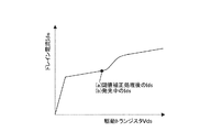
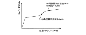
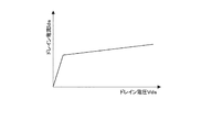
一般的に、トランジスタは、図44に示すように、ドレイン電圧(ドレイン−ソース間電圧)がある電圧に達するまでドレイン電流(ドレイン−ソース間電流)が急激に上昇し、ある電圧を超えるとドレイン電流が飽和する特性を持っている。ただし、ドレイン電流は飽和後もドレイン電圧が高くなるにつれて一定の傾きを持って直線的に上昇する。図44に示すドレイン電圧−ドレイン電流の特性は理想的な特性である。 In general, as shown in FIG. 44, in a transistor, the drain current (drain-source current) rapidly increases until the drain voltage (drain-source voltage) reaches a certain voltage. It has a characteristic that current is saturated. However, the drain current rises linearly with a certain slope as the drain voltage increases even after saturation. The drain voltage-drain current characteristics shown in FIG. 44 are ideal characteristics.
実際には、図45に示すように、飽和領域において直線性が崩れる現象、具体的にはドレイン電流が急激に上昇する、いわゆるキンク現象が起こる。キンク現象は、チャネルキャリアの衝突電離によって発生したキャリアの一部が浮遊基板に流れ込み、基板電位の変化とそれに伴う閾値電圧の低下により電流が増大する現象である。このキンク現象は、ドレイン電圧−ドレイン電流特性の線形性の低下をもたらし、出力波形にひずみが生じる原因となる。キンク現象には、製造ばらつきによって発生状態にばらつきが生じる。 Actually, as shown in FIG. 45, a phenomenon in which linearity is lost in the saturation region, specifically, a so-called kink phenomenon in which the drain current rapidly increases occurs. The kink phenomenon is a phenomenon in which part of carriers generated by impact ionization of channel carriers flows into the floating substrate, and the current increases due to a change in the substrate potential and a corresponding decrease in threshold voltage. This kink phenomenon causes a decrease in the linearity of the drain voltage-drain current characteristic and causes distortion in the output waveform. In the kink phenomenon, the occurrence state varies due to manufacturing variations.
先述した駆動トランジスタは、飽和領域で動作するように設計されている。ここで、駆動トランジスタのドレイン−ソース間電圧Vdsに注目とする、閾値補正処理後のドレイン−ソース間電圧Vdsは大きく、有機EL素子の発光中のドレイン−ソース間電圧Vdsは小さくなる。このとき、キンク現象の大きさがばらついてしまうと、ドレイン−ソース間電圧Vdsの変動がキンク現象の領域を跨ぐ場合にそのばらつきの影響を受けてしまう(その詳細については後述する)。その結果、画素間においてドレイン−ソース間電流Ids、ひいては有機EL素子の駆動電流がばらついてしまうため、画素間で輝度差が発生し、画質の悪化を招く。 The drive transistor described above is designed to operate in the saturation region. Here, focusing on the drain-source voltage Vds of the driving transistor, the drain-source voltage Vds after threshold correction processing is large, and the drain-source voltage Vds during light emission of the organic EL element is small. At this time, if the magnitude of the kink phenomenon varies, the fluctuation of the drain-source voltage Vds is affected by the variation when it crosses the kink phenomenon region (details will be described later). As a result, the drain-source current Ids and hence the driving current of the organic EL element vary between the pixels, and a luminance difference occurs between the pixels, resulting in deterioration of image quality.
そこで、本発明は、駆動トランジスタのキンク現象に起因する電気光学素子の駆動電流のばらつきを抑え、表示画像の画質を改善できるようにした表示装置、当該表示装置の駆動方法および当該表示装置を用いた電子機器を提供することを目的とする。 Therefore, the present invention uses a display device, a display device driving method, and the display device that can suppress variation in drive current of the electro-optic element due to the kink phenomenon of the drive transistor and improve the image quality of the display image. The purpose is to provide electronic devices.
上記目的を達成するために、本発明は、
電気光学素子と、
映像信号を書き込む書込みトランジスタと、
前記書込みトランジスタによって書き込まれた前記映像信号を保持する保持容量と、
前記保持容量に保持された前記映像信号に応じて前記電気光学素子を駆動する駆動トランジスタとを有し、
前記電気光学素子の発光駆動に先立って、前記駆動トランジスタのゲート電位の初期化電位を基準として当該初期化電位から前記駆動トランジスタの閾値電圧を減じた電位に向けてソース電位を変化させる閾値補正処理の機能を持つ画素が行列状に配置された表示装置の駆動に当たって、
前記駆動トランジスタに電流を供給する電源供給線の電源電位として、前記閾値補正処理を行う閾値補正期間と前記電気光学素子の発光期間とで異なる電位を設定する。
In order to achieve the above object, the present invention provides:
An electro-optic element;
A writing transistor for writing a video signal;
A holding capacitor for holding the video signal written by the writing transistor;
A driving transistor that drives the electro-optic element in accordance with the video signal held in the holding capacitor;
Prior to light emission driving of the electro-optic element, threshold correction processing for changing the source potential toward the potential obtained by subtracting the threshold voltage of the drive transistor from the initialization potential with reference to the initialization potential of the gate potential of the drive transistor In driving a display device in which pixels having the function of are arranged in a matrix,
As a power supply potential of a power supply line for supplying a current to the driving transistor, different potentials are set in a threshold correction period for performing the threshold correction process and a light emission period of the electro-optic element.
電源供給線の電源電位が閾値補正処理を行う閾値補正期間と電気光学素子の発光期間とで同じだと、閾値補正処理後と電気光学素子の発光中とで駆動トランジスタのドレイン−ソース間電圧Vdsに違いが生じる。そこで、電源供給線の電源電位を閾値補正期間と発光期間とで異ならせる。これにより、閾値補正処理後のドレイン−ソース間電圧Vdsと電気光学素子の発光中のドレイン−ソース間電圧Vdsとの違いを、電源供給線の電源電位が閾値補正期間と発光期間とで同じ場合に比べて小さくできる。その結果、駆動トランジスタにキンク現象が発生し、その発生状態に製造ばらつきによってばらつきが生じたとしても、画素間での駆動トランジスタのドレイン−ソース間電流Ids、ひいては電気光学素子の駆動電流のばらつきを小さく抑えることができる。 If the power supply potential of the power supply line is the same in the threshold correction period in which the threshold correction process is performed and the light emission period of the electro-optic element, the drain-source voltage Vds of the drive transistor is obtained after the threshold correction process and during the light emission of the electro-optic element. There is a difference. Therefore, the power supply potential of the power supply line is made different between the threshold correction period and the light emission period. Accordingly, the difference between the drain-source voltage Vds after the threshold correction processing and the drain-source voltage Vds during the light emission of the electro-optic element is the same when the power supply potential of the power supply line is the same in the threshold correction period and the light emission period. Can be smaller than As a result, a kink phenomenon occurs in the drive transistor, and even if the occurrence state varies due to manufacturing variations, the drain-source current Ids of the drive transistor between the pixels, and hence the drive current variation of the electro-optic element. It can be kept small.
本発明によれば、駆動トランジスタのキンク現象に起因する電気光学素子の駆動電流のばらつきを抑えることができるため表示画像の画質を改善できる。 According to the present invention, it is possible to suppress variation in the drive current of the electro-optic element due to the kink phenomenon of the drive transistor, and thus the image quality of the display image can be improved.
以下、発明を実施するための最良の形態(以下、「実施形態」と記述する)について図面を用いて詳細に説明する。なお、説明は以下の順序で行う。
1.本発明が適用される有機EL表示装置
2.第1実施形態(移動度補正処理を1回実行)
3.第2実施形態(移動度補正処理を2回実行)
4.変形例
5.適用例(電子機器)
Hereinafter, the best mode for carrying out the invention (hereinafter referred to as “embodiment”) will be described in detail with reference to the drawings. The description will be given in the following order.
1. 1. Organic EL display device to which the present invention is applied First Embodiment (Mobility correction processing is executed once)
3. Second Embodiment (Mobility correction processing is executed twice)
4). Modification 5 Application example (electronic equipment)
<1.本発明が適用される有機EL表示装置>
[システム構成]
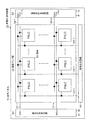
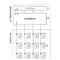
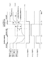
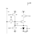
図1は、本発明が適用されるアクティブマトリクス型表示装置の構成の概略を示すシステム構成図である。ここでは、一例として、デバイスに流れる電流値に応じて発光輝度が変化する電流駆動型の電気光学素子、例えば有機EL素子を画素(画素回路)の発光素子として用いたアクティブマトリクス型有機EL表示装置の場合を例に挙げて説明するものとする。
<1. Organic EL Display Device to which the Present Invention is Applied>
[System configuration]
FIG. 1 is a system configuration diagram showing an outline of the configuration of an active matrix display device to which the present invention is applied. Here, as an example, an active matrix organic EL display device using, as an example, a current-driven electro-optical element whose emission luminance changes according to a current value flowing through the device, for example, an organic EL element as a light-emitting element of a pixel (pixel circuit) This case will be described as an example.
図1に示すように、本適用例に係る有機EL表示装置10は、発光素子を含む複数の画素20と、当該画素20が行列状に2次元配置された画素アレイ部30と、当該画素アレイ部30の周辺に配置された駆動部とを有する構成となっている。駆動部は、画素アレイ部30の各画素20を駆動する。この駆動部として、例えば、書込み走査回路40、電源供給走査回路50および信号出力回路60が設けられている。
As shown in FIG. 1, an organic EL display device 10 according to this application example includes a plurality of
ここで、有機EL表示装置10がカラー表示対応の場合は、1つの画素は複数の副画素(サブピクセル)から構成され、この副画素が画素20に相当することになる。より具体的には、カラー表示用の表示装置では、1つの画素は、赤色光(R)を発光する副画素、緑色光(G)を発光する副画素、青色光(B)を発光する副画素の3つの副画素から構成される。
Here, when the organic EL display device 10 supports color display, one pixel is composed of a plurality of sub-pixels (sub-pixels), and this sub-pixel corresponds to the
ただし、1つの画素としては、RGBの3原色の副画素の組み合わせに限られるものではなく、3原色の副画素にさらに1色あるいは複数色の副画素を加えて1つの画素を構成することも可能である。より具体的には、例えば、輝度向上のために白色光(W)を発光する副画素を加えて1つの画素を構成したり、色再現範囲を拡大するために補色光を発光する少なくとも1つの副画素を加えて1つの画素を構成したりすることも可能である。 However, one pixel is not limited to the combination of RGB three primary color subpixels, and one pixel may be configured by adding one or more color subpixels to the three primary color subpixels. Is possible. More specifically, for example, at least one sub-pixel that emits white light (W) is added to improve luminance to form one pixel, or at least one that emits complementary color light to expand the color reproduction range. It is also possible to configure one pixel by adding subpixels.
画素アレイ部30には、m行n列の画素20の配列に対して、行方向(画素行の画素の配列方向)に沿って走査線31−1〜31−mと電源供給線32−1〜32−mとが画素行ごとに配線されている。さらに、列方向(画素列の画素の配列方向)に沿って信号線33−1〜33−nが画素列ごとに配線されている。
The
走査線31−1〜31−mは、書込み走査回路40の対応する行の出力端にそれぞれ接続されている。電源供給線32−1〜32−mは、電源供給走査回路50の対応する行の出力端にそれぞれ接続されている。信号線33−1〜33−nは、信号出力回路60の対応する列の出力端にそれぞれ接続されている。
The scanning lines 31-1 to 31 -m are connected to the output ends of the corresponding rows of the writing
画素アレイ部30は、通常、ガラス基板などの透明絶縁基板上に形成されている。これにより、有機EL表示装置10は、平面型(フラット型)のパネル構造となっている。画素アレイ部30の各画素20の駆動回路は、アモルファスシリコンTFTまたは低温ポリシリコンTFTを用いて形成することができる。低温ポリシリコンTFTを用いる場合には、書込み走査回路40、電源供給走査回路50および信号出力回路60についても、画素アレイ部30を形成する表示パネル(基板)70上に実装することができる。
The
書込み走査回路40は、クロックパルスckに同期してスタートパルスspを順にシフト(転送)するシフトレジスタ等によって構成されている。この書込み走査回路40は、画素アレイ部30の各画素20への映像信号の書込みに際して、走査線31−1〜31−mに順次書込み走査信号WS(WS1〜WSm)を供給することによって画素アレイ部30の各画素20を行単位で順番に走査(線順次走査)する。
The
電源供給走査回路50は、クロックパルスckに同期してスタートパルスspを順にシフトするシフトレジスタ等によって構成されている。この電源供給走査回路50は、書込み走査回路40による線順次走査に同期して、第1電源電位Vccpと当該第1電源電位Vccpよりも低い第2電源電位Viniで切り替わる電源電位DS(DS1〜DSm)を電源供給線32−1〜32−mに供給する。この電源電位DSのVccp/Viniの切替えにより、画素20の発光/非発光の制御が行なわれる。
The power
信号出力回路60は、信号供給源(図示せず)から供給される輝度情報に応じた映像信号の信号電圧(以下、単に「信号電圧」と記述する場合もある)Vsigを選択的に出力する。信号出力回路60はさらに、後述する第1実施形態に係る表示装置の場合は基準電位Vofsを選択的に出力し、第2実施形態に係る表示装置の場合は基準電位Vofsと少なくとも1種類の中間階調電圧Vmidとを選択的に出力する(その詳細については後述する)。
The
信号出力回路60から出力される信号電圧Vsig/基準電位Vofs(または、信号電圧Vsig/基準電位Vofs/中間階調電圧Vmid)は、信号線33−1〜33−nを介して画素アレイ部30の各画素20に対して行単位で書き込まれる。すなわち、信号出力回路60は、信号電圧Vsigを行(ライン)単位で書き込む線順次書き込みの駆動形態を採っている。
The signal voltage Vsig / reference potential Vofs (or the signal voltage Vsig / reference potential Vofs / intermediate gradation voltage Vmid) output from the
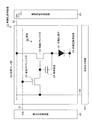
(画素回路)
図2は、画素(画素回路)20の具体的な回路構成を示す回路図である。
(Pixel circuit)
FIG. 2 is a circuit diagram showing a specific circuit configuration of the pixel (pixel circuit) 20.
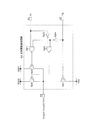
図2に示すように、画素20は、デバイスに流れる電流値に応じて発光輝度が変化する電流駆動型の電気光学素子、例えば有機EL素子21と、当該有機EL素子21を駆動する駆動回路とによって構成されている。有機EL素子21は、全ての画素20に対して共通に配線(いわゆる、ベタ配線)された共通電源供給線34にカソード電極が接続されている。
As shown in FIG. 2, the
有機EL素子21を駆動する駆動回路は、駆動トランジスタ22、書込みトランジスタ23および保持容量24を有する構成となっている。ここでは、駆動トランジスタ22および書込みトランジスタ23としてNチャネル型のTFTを用いている。ただし、駆動トランジスタ22および書込みトランジスタ23の導電型の組み合わせは一例に過ぎず、これらの組み合わせに限られるものではない。
The drive circuit that drives the
なお、駆動トランジスタ22および書込みトランジスタ23としてNチャネル型のTFTを用いると、アモルファスシリコン(a−Si)プロセスを用いることができる。a−Siプロセスを用いることで、TFTを作成する基板の低コスト化、ひいては本有機EL表示装置10の低コスト化を図ることが可能になる。また、駆動トランジスタ22および書込みトランジスタ23を同じ導電型の組み合わせにすると、両トランジスタ22,23を同じプロセスで作成することができるため低コスト化に寄与できる。
Note that when an N-channel TFT is used as the driving
駆動トランジスタ22は、一方の電極(ソース/ドレイン電極)が有機EL素子21のアノード電極に接続され、他方の電極(ドレイン/ソース電極)が電源供給線32(32−1〜32−m)に接続されている。
The
書込みトランジスタ23は、一方の電極(ソース/ドレイン電極)が信号線33(33−1〜33−n)に接続され、他方の電極(ドレイン/ソース電極)が駆動トランジスタ22のゲート電極に接続されている。また、書込みトランジスタ23のゲート電極は、走査線31(31−1〜31−m)に接続されている。
The
駆動トランジスタ22および書込みトランジスタ23において、一方の電極とは、ソース/ドレイン領域に電気的に接続された金属配線を言い、他方の電極とは、ドレイン/ソース領域に電気的に接続された金属配線を言う。また、一方の電極と他方の電極との電位関係によって一方の電極がソース電極ともなればドレイン電極ともなり、他方の電極がドレイン電極ともなればソース電極ともなる。
In the
保持容量24は、一方の電極が駆動トランジスタ22のゲート電極に接続され、他方の電極が駆動トランジスタ22の他方の電極および有機EL素子21のアノード電極に接続されている。
The
なお、有機EL素子21の駆動回路としては、駆動トランジスタ22および書込みトランジスタ23の2つのトランジスタと保持容量24の1つの容量素子とからなる回路構成のものに限られるものではない。例えば、一方の電極が有機EL素子21のアノード電極に、他方の電極が固定電位にそれぞれ接続されることで、有機EL素子21の容量不足分を補う補助容量を必要に応じて設けた回路構成を採ることも可能である。
The drive circuit of the
上記構成の画素20において、書込みトランジスタ23は、書込み走査回路40から走査線31を通してゲート電極に印加されるHighアクティブの書込み走査信号WSに応答して導通状態となる。これにより、書込みトランジスタ23は、信号線33を通して信号出力回路60から供給される輝度情報に応じた映像信号の信号電圧Vsigまたは基準電位Vofs(または、Vofs1/Vofs2)をサンプリングして画素20内に書き込む。この書き込まれた信号電圧Vsigまたは基準電位Vofs(または、信号電圧Vsig/基準電位Vofs/中間階調電圧Vmid)は、駆動トランジスタ22のゲート電極に印加されるとともに保持容量24に保持される。
In the
駆動トランジスタ22は、電源供給線32(32−1〜32−m)の電位DSが第1電源電位Vccpにあるときには、一方の電極がドレイン電極、他方の電極がソース電極となって飽和領域で動作する。これにより、駆動トランジスタ22は、電源供給線32から電流の供給を受けて有機EL素子21を電流駆動にて発光駆動する。より具体的には、駆動トランジスタ22は、飽和領域で動作することにより、保持容量24に保持された信号電圧Vsigの電圧値に応じた電流値の駆動電流を有機EL素子21に供給し、当該有機EL素子21を電流駆動することによって発光させる。
When the potential DS of the power supply line 32 (32-1 to 32-m) is at the first power supply potential Vccp, the
駆動トランジスタ22はさらに、電源電位DSが第1電源電位Vccpから第2電源電位Viniに切り替わったときには、一方の電極がソース電極、他方の電極がドレイン電極となってスイッチングトランジスタとして動作する。これにより、駆動トランジスタ22は、有機EL素子21への駆動電流の供給を停止し、有機EL素子21を非発光状態にする。すなわち、駆動トランジスタ22は、有機EL素子21の発光/非発光を制御するトランジスタとしての機能をも併せ持っている。
Further, when the power supply potential DS is switched from the first power supply potential Vccp to the second power supply potential Vini, the
この駆動トランジスタ22のスイッチング動作により、有機EL素子21が非発光状態となる期間(非発光期間)を設け、有機EL素子21の発光期間と非発光期間の割合(デューティ)を制御する。このデューティ制御により、1フレーム期間に亘って画素が発光することに伴う残像ボケを低減できるために、特に動画の画品位をより優れたものとすることができる。
By the switching operation of the
ここで、信号出力回路60から信号線33を通して選択的に供給される基準電位Vofs(または、信号電圧Vsig/基準電位Vofs/中間階調電圧Vmid)は、輝度情報に応じた映像信号の信号電圧Vsigの基準となる電位(例えば、映像信号の黒レベルに相当する電位)である。
Here, the reference potential Vofs (or signal voltage Vsig / reference potential Vofs / intermediate gradation voltage Vmid) selectively supplied from the
電源供給走査回路50から電源供給線32を通して選択的に供給される第1,第2電源電位Vccp,Viniのうち、第1電源電位Vccpは有機EL素子21を発光駆動する駆動電流を駆動トランジスタ22に供給するための電源電位である。また、第2電源電位Viniは、有機EL素子21に対して逆バイアスを掛けるための電源電位である。この第2電源電位Viniは、基準電位Vofsよりも低い電位、例えば、駆動トランジスタ22の閾値電圧をVthとするときVofs−Vthよりも低い電位、好ましくはVofs−Vthよりも十分に低い電位に設定される。
Of the first and second power supply potentials Vccp and Vini selectively supplied from the power
(画素構造)
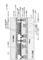
図3は、画素20の断面構造の一例を示す断面図である。図3に示すように、ガラス基板201上には、駆動トランジスタ22等を含む駆動回路が形成されている。そして、画素20は、ガラス基板201上に絶縁膜202、絶縁平坦化膜203およびウインド絶縁膜204がその順に形成され、当該ウインド絶縁膜204の凹部204Aに有機EL素子21が設けられた構成となっている。ここでは、駆動回路の各構成素子のうち、駆動トランジスタ22のみを図示し、他の構成素子については省略している。
(Pixel structure)
FIG. 3 is a cross-sectional view illustrating an example of the cross-sectional structure of the
有機EL素子21は、アノード電極205と、有機層(電子輸送層、発光層、ホール輸送層/ホール注入層)206と、カソード電極207とから構成されている。アノード電極205は、ウインド絶縁膜204の凹部204Aの底部に形成された金属等からなる。有機層206は、アノード電極205上に形成されている。カソード電極207は、有機層206上に全画素共通に形成された透明導電膜等からなる。
The
この有機EL素子21において、有機層206は、アノード電極205上にホール輸送層/ホール注入層2061、発光層2062、電子輸送層2063および電子注入層(図示せず)が順次堆積されることによって形成される。そして、図2の駆動トランジスタ22による電流駆動の下に、駆動トランジスタ22からアノード電極205を通して有機層206に電流が流れることで、当該有機層206内の発光層2062において電子と正孔が再結合する際に発光するようになっている。
In the
駆動トランジスタ22は、ゲート電極221と、半導体層222の両側に設けられたソース/ドレイン領域223,224と、半導体層222のゲート電極221と対向する部分のチャネル形成領域225とから構成されている。ソース/ドレイン領域223は、コンタクトホールを介して有機EL素子21のアノード電極205と電気的に接続されている。
The
そして、図3に示すように、ガラス基板201上に、絶縁膜202、絶縁平坦化膜203およびウインド絶縁膜204を介して有機EL素子21が画素単位で形成された後は、パッシベーション膜208を介して封止基板209が接着剤210によって接合される。この封止基板209によって有機EL素子21が封止されることにより表示パネル70が形成される。
Then, as shown in FIG. 3, after the
<2.第1実施形態>
本発明は、以上説明したシステム構成を基本とする有機EL表示装置10を前提としている。そして、本発明の第1実施形態に係る有機EL表示装置10Aは、信号出力回路60が映像信号の信号電圧Vsigと基準電位Vofsとを選択的に出力する構成となっている。基準電位Vofsは、先述したように、映像信号の信号電圧Vsigの基準となる電位である。
<2. First Embodiment>
The present invention is based on the organic EL display device 10 based on the system configuration described above. In the organic EL display device 10A according to the first embodiment of the present invention, the
[回路動作]
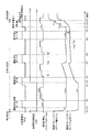
続いて、第1実施形態に係る有機EL表示装置10Aの基本的な回路動作について、図4のタイミング波形図を基に図5および図6の動作説明図を用いて説明する。なお、図5および図6の動作説明図では、図面の簡略化のために、書込みトランジスタ23をスイッチのシンボルで図示している。また、有機EL素子21の等価容量25についても図示している。
[Circuit operation]
Next, the basic circuit operation of the organic EL display device 10A according to the first embodiment will be described with reference to the operation waveform diagrams of FIGS. 5 and 6 based on the timing waveform diagram of FIG. In the operation explanatory diagrams of FIGS. 5 and 6, the
図4のタイミング波形図には、走査線31の電位(書込み走査信号)WS、電源供給線32の電位(電源電位)DS、信号線33の電位(Vsig/Vofs)、駆動トランジスタ22のゲート電位Vgおよびソース電位Vsのそれぞれの変化を示している。
In the timing waveform diagram of FIG. 4, the potential of the scanning line 31 (write scanning signal) WS, the potential of the power supply line 32 (power supply potential) DS, the potential of the signal line 33 (Vsig / Vofs), and the gate potential of the driving
(前フレームの発光期間)
図4のタイミング波形図において、時刻t11以前は、前のフレーム(フィールド)における有機EL素子21の発光期間となる。この前フレームの発光期間では、電源供給線32の電位DSが第1電源電位(以下、「高電位」と記述する)Vccpにあり、また、書込みトランジスタ23が非導通状態にある。
(Prior frame emission period)
In the timing waveform diagram of FIG. 4, the period before time t11 is the light emission period of the
このとき、駆動トランジスタ22は飽和領域で動作するように設計されている。これにより、図5(A)に示すように、駆動トランジスタ22のゲート−ソース間電圧Vgsに応じた駆動電流(ドレイン−ソース間電流)Idsが、電源供給線32から駆動トランジスタ22を通して有機EL素子21に供給される。よって、有機EL素子21が駆動電流Idsの電流値に応じた輝度で発光する。
At this time, the
(閾値補正準備期間)
時刻t11になると、線順次走査の新しいフレーム(現フレーム)に入る。そして、図5(B)に示すように、電源供給線32の電位DSが高電位Vccpから、信号線33の基準電位Vofsに対してVofs−Vthよりも十分に低い第2電源電位(以下、「低電位」と記述する)Viniに切り替わる。
(Threshold correction preparation period)
At time t11, a new frame (current frame) for line sequential scanning is entered. As shown in FIG. 5B, the second power supply potential (hereinafter, referred to as the potential DS of the
ここで、有機EL素子21の閾値電圧をVthel、共通電源供給線34の電位(カソード電位)をVcathとする。このとき、低電位ViniをVini<Vthel+Vcathとすると、駆動トランジスタ22のソース電位Vsが低電位Viniにほぼ等しくなるために、有機EL素子21は逆バイアス状態となって消光する。
Here, the threshold voltage of the
次に、時刻t12で走査線31の電位WSが低電位側から高電位側に遷移することで、図5(C)に示すように、書込みトランジスタ23が導通状態となる。このとき、信号出力回路60から信号線33に対して基準電位Vofsが供給されているために、駆動トランジスタ22のゲート電位Vgが基準電位Vofsになる。また、駆動トランジスタ22のソース電位Vsは、基準電位Vofsよりも十分に低い電位Viniにある。
Next, at time t12, the potential WS of the scanning line 31 transitions from the low potential side to the high potential side, so that the writing
このとき、駆動トランジスタ22のゲート−ソース間電圧VgsはVofs−Viniとなる。ここで、Vofs−Viniが駆動トランジスタ22の閾値電圧Vthよりも大きくないと、後述する閾値補正処理を行うことができないために、Vofs−Vini>Vthなる電位関係に設定する必要がある。
At this time, the gate-source voltage Vgs of the
このように、駆動トランジスタ22のゲート電位Vgを基準電位Vofsに、ソース電位Vsを低電位Viniにそれぞれ固定して(確定させて)初期化する処理が、後述する閾値補正処理を行う前の準備(閾値補正準備)の処理である。したがって、基準電位Vofsおよび低電位Viniが、駆動トランジスタ22のゲート電位Vgおよびソース電位Vsの各初期化電位となる。
As described above, the process of fixing (initializing) the gate potential Vg of the
(閾値補正期間)
次に、時刻t13で、図5(D)に示すように、電源供給線32の電位DSが低電位Viniから高電位Vccpに切り替わると、駆動トランジスタ22のゲート電位Vgが保たれた状態で閾値補正処理が開始される。すなわち、ゲート電位Vgから駆動トランジスタ22の閾値電圧Vthを減じた電位に向けて駆動トランジスタ22のソース電位Vsが上昇を開始する。
(Threshold correction period)
Next, at time t13, as shown in FIG. 5D, when the potential DS of the
ここでは、便宜上、駆動トランジスタ22のゲート電極の初期化電位Vofsを基準として、当該初期化電位Vofsから駆動トランジスタ22の閾値電圧Vthを減じた電位に向けてソース電位Vsを変化させる処理を閾値補正処理と呼んでいる。この閾値補正処理が進むと、やがて、駆動トランジスタ22のゲート−ソース間電圧Vgsが駆動トランジスタ22の閾値電圧Vthに収束する。この閾値電圧Vthに相当する電圧は保持容量24に保持される。
Here, for convenience, processing for changing the source potential Vs toward the potential obtained by subtracting the threshold voltage Vth of the
なお、閾値補正処理を行う期間(閾値補正期間)において、電流が専ら保持容量24側に流れ、有機EL素子21側には流れないようにするために、有機EL素子21がカットオフ状態となるように共通電源供給線34の電位Vcathを設定しておくこととする。
In the period for performing the threshold correction process (threshold correction period), the
次に、時刻t14で走査線31の電位WSが低電位側に遷移することで、図6(A)に示すように、書込みトランジスタ23が非導通状態となる。このとき、駆動トランジスタ22のゲート電極が信号線33から電気的に切り離されることによってフローティング状態になる。しかし、ゲート−ソース間電圧Vgsが駆動トランジスタ22の閾値電圧Vthに等しいために、当該駆動トランジスタ22はカットオフ状態にある。したがって、駆動トランジスタ22にドレイン−ソース間電流Idsは流れない。
Next, when the potential WS of the scanning line 31 transits to a low potential side at time t14, the writing
(信号書込み&移動度補正期間)
次に、時刻t15で、図6(B)に示すように、信号線33の電位が基準電位Vofsから映像信号の信号電圧Vsigに切り替わる。続いて、時刻t16で、走査線31の電位WSが高電位側に遷移することで、図6(C)に示すように、書込みトランジスタ23が導通状態になって映像信号の信号電圧Vsigをサンプリングして画素20内に書き込む。
(Signal writing & mobility correction period)
Next, at time t15, as shown in FIG. 6B, the potential of the
この書込みトランジスタ23による信号電圧Vsigの書込みにより、駆動トランジスタ22のゲート電位Vgが信号電圧Vsigとなる。そして、映像信号の信号電圧Vsigによる駆動トランジスタ22の駆動の際に、当該駆動トランジスタ22の閾値電圧Vthが保持容量24に保持された閾値電圧Vthに相当する電圧と相殺される。この閾値キャンセルの原理の詳細については後述する。
By the writing of the signal voltage Vsig by the writing
このとき、有機EL素子21はカットオフ状態(ハイインピーダンス状態)にある。したがって、映像信号の信号電圧Vsigに応じて電源供給線32から駆動トランジスタ22に流れる電流(ドレイン−ソース間電流Ids)は有機EL素子21の等価容量25に流れ込み、当該等価容量25の充電が開始される。
At this time, the
有機EL素子21の等価容量25の充電により、駆動トランジスタ22のソース電位Vsが時間の経過と共に上昇していく。このとき既に、駆動トランジスタ22の閾値電圧Vthの画素ごとのばらつきがキャンセルされており、駆動トランジスタ22のドレイン−ソース間電流Idsは当該駆動トランジスタ22の移動度μに依存したものとなる。
As the
ここで、映像信号の信号電圧Vsigに対する保持容量24の保持電圧Vgsの比率、即ち書込みゲインGが1(理想値)であると仮定する。すると、駆動トランジスタ22のソース電位VsがVofs−Vth+ΔVの電位まで上昇することで、駆動トランジスタ22のゲート‐ソース間電圧VgsはVsig−Vofs+Vth−ΔVとなる。
Here, it is assumed that the ratio of the holding voltage Vgs of the holding
すなわち、駆動トランジスタ22のソース電位Vsの上昇分ΔVは、保持容量24に保持された電圧(Vsig−Vofs+Vth)から差し引かれるように、換言すれば、保持容量24の充電電荷を放電するように作用し、負帰還がかけられたことになる。したがって、ソース電位Vsの上昇分ΔVは負帰還の帰還量となる。
That is, the increase ΔV of the source potential Vs of the
このように、駆動トランジスタ22に流れるドレイン−ソース間電流Idsに応じた帰還量ΔVでゲート‐ソース間電圧Vgsに負帰還をかけることで、駆動トランジスタ22のドレイン−ソース間電流Idsの移動度μに対する依存性を打ち消すことができる。この打ち消す処理が、駆動トランジスタ22の移動度μの画素ごとのばらつきを補正する移動度補正処理である。
In this way, by applying negative feedback to the gate-source voltage Vgs with a feedback amount ΔV corresponding to the drain-source current Ids flowing through the
より具体的には、駆動トランジスタ22のゲート電極に書き込まれる映像信号の信号振幅Vin(=Vsig−Vofs)が高いほどドレイン−ソース間電流Idsが大きくなるために、負帰還の帰還量ΔVの絶対値も大きくなる。したがって、発光輝度レベルに応じた移動度補正処理が行われる。
More specifically, since the drain-source current Ids increases as the signal amplitude Vin (= Vsig−Vofs) of the video signal written to the gate electrode of the
また、映像信号の信号振幅Vinを一定とした場合、駆動トランジスタ22の移動度μが大きいほど負帰還の帰還量ΔVの絶対値も大きくなるために、画素ごとの移動度μのばらつきを取り除くことができる。したがって、負帰還の帰還量ΔVは移動度補正の補正量とも言える。移動度補正の原理の詳細については後述する。
Further, when the signal amplitude Vin of the video signal is constant, the absolute value of the feedback amount ΔV of the negative feedback increases as the mobility μ of the
(発光期間)
次に、時刻t17で走査線31の電位WSが低電位側に遷移することで、図6(D)に示すように、書込みトランジスタ23が非導通状態となる。これにより、駆動トランジスタ22のゲート電極は、信号線33から電気的に切り離されるためにフローティング状態になる。
(Light emission period)
Next, at time t17, the potential WS of the scanning line 31 transitions to the low potential side, so that the writing
ここで、駆動トランジスタ22のゲート電極がフローティング状態にあるときは、駆動トランジスタ22のゲート−ソース間に保持容量24が接続されていることにより、駆動トランジスタ22のソース電位Vsの変動に連動してゲート電位Vgも変動する。このように、駆動トランジスタ22のゲート電位Vgがソース電位Vsの変動に連動して変動する動作が、保持容量24によるブートストラップ動作である。
Here, when the gate electrode of the driving
駆動トランジスタ22のゲート電極がフローティング状態になり、それと同時に、駆動トランジスタ22のドレイン−ソース間電流Idsが有機EL素子21に流れ始めることにより、当該電流Idsに応じて有機EL素子21のアノード電位が上昇する。
The gate electrode of the
そして、有機EL素子21のアノード電位がVthel+Vcathを越えると、有機EL素子21に駆動電流が流れ始めるため有機EL素子21が発光を開始する。また、有機EL素子21のアノード電位の上昇は、即ち駆動トランジスタ22のソース電位Vsの上昇に他ならない。駆動トランジスタ22のソース電位Vsが上昇すると、保持容量24のブートストラップ動作により、駆動トランジスタ22のゲート電位Vgも連動して上昇する。
When the anode potential of the
このとき、ブートストラップゲインが1(理想値)であると仮定した場合、ゲート電位Vgの上昇量はソース電位Vsの上昇量に等しくなる。故に、発光期間中駆動トランジスタ22のゲート‐ソース間電圧VgsはVsig−Vofs+Vth−ΔVで一定に保持される。そして、時刻t18で信号線33の電位が映像信号の信号電圧Vsigから基準電位Vofsに切り替わる。
At this time, assuming that the bootstrap gain is 1 (ideal value), the amount of increase in the gate potential Vg is equal to the amount of increase in the source potential Vs. Therefore, the gate-source voltage Vgs of the
以上説明した一連の回路動作において、閾値補正準備、閾値補正、信号電圧Vsigの書込み(信号書込み)および移動度補正の各処理動作は、1水平走査期間(1H)において実行される。また、信号書込みおよび移動度補正の各処理動作は、時刻t6−t7の期間において並行して実行される。 In the series of circuit operations described above, each processing operation of threshold correction preparation, threshold correction, signal voltage Vsig writing (signal writing), and mobility correction is executed in one horizontal scanning period (1H). Further, the signal writing and mobility correction processing operations are executed in parallel during the period from time t6 to time t7.
なお、ここでは、閾値補正処理を1回だけ実行する駆動法を採る場合を例に挙げて説明したが、この駆動法は一例に過ぎず、この駆動法に限られるものではない。例えば、閾値補正処理を移動度補正および信号書込み処理と共に行う1H期間に加えて、当該1H期間に先行する複数の水平走査期間に亘って分割して複数回実行する、いわゆる分割Vth補正を行う駆動法を採ることも可能である。 Here, the case where the driving method in which the threshold value correction process is executed only once is described as an example, but this driving method is only an example and is not limited to this driving method. For example, in addition to a 1H period in which threshold correction processing is performed together with mobility correction and signal writing processing, driving that performs so-called divided Vth correction that is executed a plurality of times divided over a plurality of horizontal scanning periods preceding the 1H period. It is also possible to take the law.
この分割Vth補正の駆動法を採用することにより、高精細化に伴う多画素化によって1水平走査期間に割り当てられる時間が短くなったとしても、閾値補正期間として複数の水平走査期間に亘って十分な時間を確保することができるために、閾値補正処理を確実に行うことができる。 By adopting this divided Vth correction driving method, even if the time allotted to one horizontal scanning period is shortened due to the increase in the number of pixels accompanying high definition, the threshold correction period is sufficient for a plurality of horizontal scanning periods. Since a sufficient time can be secured, the threshold correction process can be performed reliably.
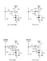
〔閾値キャンセルの原理〕
ここで、駆動トランジスタ22の閾値キャンセル(即ち、閾値補正)の原理について説明する。駆動トランジスタ22は、飽和領域で動作するように設計されているために定電流源として動作する。これにより、有機EL素子21には駆動トランジスタ22から、次式(1)で与えられる一定のドレイン−ソース間電流(駆動電流)Idsが供給される。
Ids=(1/2)・μ(W/L)Cox(Vgs−Vth)2 ……(1)
ここで、Wは駆動トランジスタ22のチャネル幅、Lはチャネル長、Coxは単位面積当たりのゲート容量である。
[Principle of threshold cancellation]
Here, the principle of threshold cancellation (that is, threshold correction) of the
Ids = (1/2) · μ (W / L) Cox (Vgs−Vth) 2 (1)
Here, W is the channel width of the
図7に、駆動トランジスタ22のドレイン−ソース間電流Ids対ゲート−ソース間電圧Vgsの特性を示す。
FIG. 7 shows characteristics of the drain-source current Ids of the
この特性図に示すように、駆動トランジスタ22の閾値電圧Vthの画素ごとのばらつきに対するキャンセル処理を行わないと、閾値電圧VthがVth1のとき、ゲート−ソース間電圧Vgsに対応するドレイン−ソース間電流IdsがIds1になる。
As shown in this characteristic diagram, if no cancellation process is performed for the variation of the threshold voltage Vth of the
これに対して、閾値電圧VthがVth2(Vth2>Vth1)のとき、同じゲート−ソース間電圧Vgsに対応するドレイン−ソース間電流IdsがIds2(Ids2<Ids)になる。すなわち、駆動トランジスタ22の閾値電圧Vthが変動すると、ゲート−ソース間電圧Vgsが一定であってもドレイン−ソース間電流Idsが変動する。
On the other hand, when the threshold voltage Vth is Vth2 (Vth2> Vth1), the drain-source current Ids corresponding to the same gate-source voltage Vgs is Ids2 (Ids2 <Ids). That is, when the threshold voltage Vth of the
一方、上記構成の画素(画素回路)20では、先述したように、発光時の駆動トランジスタ22のゲート−ソース間電圧VgsはVsig−Vofs+Vth−ΔVである。したがって、これを式(1)に代入すると、ドレイン−ソース間電流Idsは、次式(2)で表される。
Ids=(1/2)・μ(W/L)Cox(Vsig−Vofs−ΔV)2
……(2)
On the other hand, in the pixel (pixel circuit) 20 having the above configuration, as described above, the gate-source voltage Vgs of the
Ids = (1/2) · μ (W / L) Cox (Vsig−Vofs−ΔV) 2
(2)
すなわち、駆動トランジスタ22の閾値電圧Vthの項がキャンセルされており、駆動トランジスタ22から有機EL素子21に供給されるドレイン−ソース間電流Idsは、駆動トランジスタ22の閾値電圧Vthに依存しない。その結果、駆動トランジスタ22の製造プロセスのばらつきや経時変化により、駆動トランジスタ22の閾値電圧Vthが画素ごとに変動したとしても、ドレイン−ソース間電流Idsが変動しないために、有機EL素子21の発光輝度を一定に保つことができる。
That is, the term of the threshold voltage Vth of the
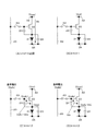
〔移動度補正の原理〕
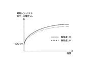
次に、駆動トランジスタ22の移動度補正の原理について説明する。図8に、駆動トランジスタ22の移動度μが相対的に大きい画素Aと、駆動トランジスタ22の移動度μが相対的に小さい画素Bとを比較した状態で特性カーブを示す。駆動トランジスタ22をポリシリコン薄膜トランジスタなどで構成した場合、画素Aや画素Bのように、画素間で移動度μがばらつくことは避けられない。
[Principle of mobility correction]
Next, the principle of mobility correction of the
画素Aと画素Bで移動度μにばらつきがある状態で、駆動トランジスタ22のゲート電極に例えば両画素A,Bに同レベルの信号振幅Vin(=Vsig−Vofs)を書き込んだ場合を考える。この場合、何ら移動度μの補正を行わないと、移動度μの大きい画素Aに流れるドレイン−ソース間電流Ids1′と移動度μの小さい画素Bに流れるドレイン−ソース間電流Ids2′との間には大きな差が生じてしまう。このように、移動度μの画素ごとのばらつきに起因してドレイン−ソース間電流Idsに画素間で大きな差が生じると、画面のユニフォーミティが損なわれる。
Consider a case where the signal amplitude Vin (= Vsig−Vofs) of the same level is written to both the pixels A and B, for example, in the gate electrode of the
ここで、先述した式(1)のトランジスタ特性式から明らかなように、移動度μが大きいとドレイン−ソース間電流Idsが大きくなる。したがって、負帰還における帰還量ΔVは移動度μが大きくなるほど大きくなる。図8に示すように、移動度μの大きな画素Aの帰還量ΔV1は、移動度の小さな画素Bの帰還量ΔV2に比べて大きい。 Here, as is clear from the transistor characteristic equation of Equation (1), the drain-source current Ids increases when the mobility μ is large. Therefore, the feedback amount ΔV in the negative feedback increases as the mobility μ increases. As shown in FIG. 8, the feedback amount ΔV1 of the pixel A having a high mobility μ is larger than the feedback amount ΔV2 of the pixel B having a low mobility.
そこで、移動度補正処理によって駆動トランジスタ22のドレイン−ソース間電流Idsに応じた帰還量ΔVでゲート−ソース間電圧Vgsに負帰還をかけることにより、移動度μが大きいほど負帰還が大きくかかることになる。その結果、移動度μの画素ごとのばらつきを抑制することができる。
Therefore, by applying negative feedback to the gate-source voltage Vgs with the feedback amount ΔV corresponding to the drain-source current Ids of the
具体的には、移動度μの大きな画素Aで帰還量ΔV1の補正をかけると、ドレイン−ソース間電流IdsはIds1′からIds1まで大きく下降する。一方、移動度μの小さな画素Bの帰還量ΔV2は小さいために、ドレイン−ソース間電流IdsはIds2′からIds2までの下降となり、それ程大きく下降しない。結果的に、画素Aのドレイン−ソース間電流Ids1と画素Bのドレイン−ソース間電流Ids2とはほぼ等しくなるために、移動度μの画素ごとのばらつきが補正される。 Specifically, when the feedback amount ΔV1 is corrected in the pixel A having a high mobility μ, the drain-source current Ids greatly decreases from Ids1 ′ to Ids1. On the other hand, since the feedback amount ΔV2 of the pixel B having a low mobility μ is small, the drain-source current Ids decreases from Ids2 ′ to Ids2, and does not decrease that much. As a result, since the drain-source current Ids1 of the pixel A and the drain-source current Ids2 of the pixel B are substantially equal, the variation in mobility μ from pixel to pixel is corrected.
以上をまとめると、移動度μの異なる画素Aと画素Bがあった場合、移動度μの大きい画素Aの帰還量ΔV1は移動度μの小さい画素Bの帰還量ΔV2に比べて大きくなる。つまり、移動度μが大きい画素ほど帰還量ΔVが大きく、ドレイン−ソース間電流Idsの減少量が大きくなる。 In summary, when there are a pixel A and a pixel B having different mobility μ, the feedback amount ΔV1 of the pixel A having a high mobility μ is larger than the feedback amount ΔV2 of the pixel B having a low mobility μ. That is, the larger the mobility μ, the larger the feedback amount ΔV, and the larger the amount of decrease in the drain-source current Ids.
したがって、駆動トランジスタ22のドレイン−ソース間電流Idsに応じた帰還量ΔVで、ゲート−ソース間電圧Vgsに負帰還をかけることで、移動度μの異なる画素のドレイン−ソース間電流Idsの電流値が均一化される。その結果、移動度μの画素ごとのばらつきを補正することができる。すなわち、駆動トランジスタ22に流れる電流(ドレイン−ソース間電流Ids)に応じた帰還量ΔVで、駆動トランジスタ22のゲート−ソース間電圧Vgsに負帰還をかける処理が移動度補正処理となる。
Therefore, by applying negative feedback to the gate-source voltage Vgs with a feedback amount ΔV corresponding to the drain-source current Ids of the driving
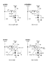
ここで、図2に示した画素(画素回路)20において、閾値補正、移動度補正の有無による映像信号の信号電圧Vsigと駆動トランジスタ22のドレイン・ソース間電流Idsとの関係について図9を用いて説明する。
Here, in the pixel (pixel circuit) 20 shown in FIG. 2, the relationship between the signal voltage Vsig of the video signal and the drain-source current Ids of the
図9において、(A)は閾値補正および移動度補正を共に行わない場合、(B)は移動度補正を行わず、閾値補正のみを行った場合、(C)は閾値補正および移動度補正を共に行った場合をそれぞれ示している。図9(A)に示すように、閾値補正および移動度補正を共に行わない場合には、閾値電圧Vthおよび移動度μの画素A,Bごとのばらつきに起因してドレイン−ソース間電流Idsに画素A,B間で大きな差が生じることになる。 In FIG. 9, (A) does not perform both threshold correction and mobility correction, (B) does not perform mobility correction, and performs only threshold correction, (C) performs threshold correction and mobility correction. Each case is shown. As shown in FIG. 9A, when neither threshold correction nor mobility correction is performed, the drain-source current Ids is caused by variations in the threshold voltage Vth and the mobility μ for each of the pixels A and B. A large difference occurs between the pixels A and B.
これに対し、閾値補正のみを行った場合は、図9(B)に示すように、ドレイン−ソース間電流Idsのばらつきをある程度低減できるものの、移動度μの画素A,Bごとのばらつきに起因する画素A,B間でのドレイン−ソース間電流Idsの差は残る。そして、閾値補正および移動度補正を共に行うことで、図9(C)に示すように、閾値電圧Vthおよび移動度μの画素A,Bごとのばらつきに起因する画素A,B間でのドレイン−ソース間電流Idsの差をほぼ無くすことができる。したがって、どの階調においても有機EL素子21の輝度ばらつきは発生せず、良好な画質の表示画像を得ることができる。
On the other hand, when only the threshold correction is performed, as shown in FIG. 9B, although the variation in the drain-source current Ids can be reduced to some extent, it is caused by the variation in the mobility μ between the pixels A and B. The difference between the drain-source current Ids between the pixels A and B to be left remains. Then, by performing both the threshold correction and the mobility correction, as shown in FIG. 9C, the drain between the pixels A and B due to the variation of the threshold voltage Vth and the mobility μ for each of the pixels A and B. -The difference in the current Ids between the sources can be almost eliminated. Therefore, the luminance variation of the
また、図2に示した画素20は、閾値補正および移動度補正の各補正機能に加えて、先述した保持容量24によるブートストラップ動作の機能を備えていることで、次のような作用効果を得ることができる。
Further, the
すなわち、有機EL素子21のI−V特性の経時変化に伴って駆動トランジスタ22のソース電位Vsが変化したとしても、保持容量24によるブートストラップ動作により、駆動トランジスタ22のゲート−ソース間電位Vgsを一定に維持することができる。したがって、有機EL素子21に流れる電流は変化せず一定となる。その結果、有機EL素子21の発光輝度も一定に保たれるために、有機EL素子21のI−V特性が経時変化したとしても、それに伴う輝度劣化のない画像表示を実現できる。
That is, even if the source potential Vs of the
[キンク現象に起因する駆動電流のばらつきについて]
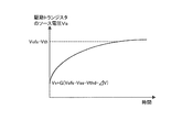
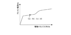
ここで、有機EL素子21に駆動電流を流すときに、飽和領域で動作するように設計されている駆動トランジスタ22のドレイン−ソース間電圧Vdsについて、図10のタイミング波形図を用いて考える。
[Difference in drive current due to kink phenomenon]
Here, the drain-source voltage Vds of the
図10には、図2に示す駆動トランジスタ22のドレイン電位Vd、ゲート電位Vg、ソース電位Vsについてその波形を示している。駆動トランジスタ22のドレイン電位Vdは電源供給線32の電源電位である。
FIG. 10 shows waveforms of the drain potential Vd, gate potential Vg, and source potential Vs of the
先述した動作説明から明らかなように、閾値補正処理の終了後、映像信号の信号電圧Vsigが書き込まれると、駆動トランジスタ22のゲート電位Vgが上昇し、それに伴ってソース電位Vsも上昇する。その後も、移動度補正処理が行われることでソース電位Vsが上昇し、発光期間においても負帰還がかかることによってソース電位Vsがさらに上昇する。したがって、図10のタイミング波形図から明らかなように、閾値補正処理後のドレイン−ソース間電圧Vds(a)は大きく、有機EL素子21の発光中のドレイン−ソース間電圧Vds(b)は小さくなる。
As is apparent from the above-described operation description, when the signal voltage Vsig of the video signal is written after the threshold correction process is finished, the gate potential Vg of the
ここで、駆動トランジスタ22の特性が、図11に示す理想的なトランジスタ特性であるとする。この場合、飽和領域においてドレイン電流Idsがドレイン−ソース間電圧Vdsに対して傾きが一定で変化するため、ドレイン−ソース間電圧Vdsが変動しても画素間のドレイン電流Idsの変動分ΔIdsの差分が小さい。したがって、ドレイン−ソース間電圧Vdsが変動しても、画素間で有機EL素子21の駆動電流のばらつきが起きにくい。
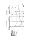
Here, it is assumed that the characteristics of the driving
駆動トランジスタ22の飽和領域では、Vds>Vgs−Vthの電位関係にある。ここで、駆動トランジスタ22のチャネル変調係数をλとすると、駆動トランジスタ22のドレイン−ソース間電流Idsは、次式(3)で表される。
Ids=(1/2)・μ(W/L)Cox(Vgs−Vth)2
・(1+λVds) ……(3)
In the saturation region of the
Ids = (1/2) · μ (W / L) Cox (Vgs−Vth) 2
・ (1 + λVds) (3)
これに対して、駆動トランジスタ22の特性が図12に示すトランジスタ特性、即ちキンク現象が発生するトランジスタ特性の場合には次のようになる。
On the other hand, when the characteristics of the driving
キンク現象の発生状態は、製造ばらつき等によってトランジスタごとにばらつく。ここに、キンク現象の発生状態とは、ドレイン電流Idsが急激に変化するときの変化量やキンク現象の立ち上がりのタイミング等をいう。このように、キンク現象の変化量やキンク現象の立ち上がりのタイミング等、キンク現象の発生状態がトランジスタごとにばらついてしまうと、ドレイン−ソース間電圧Vdsの変動がキンク現象の領域を跨ぐ場合にそのばらつきの影響を受けてしまう。 The state of occurrence of the kink phenomenon varies from transistor to transistor due to manufacturing variations and the like. Here, the occurrence state of the kink phenomenon means the amount of change when the drain current Ids changes abruptly, the rise timing of the kink phenomenon, and the like. As described above, when the state of occurrence of the kink phenomenon, such as the amount of change of the kink phenomenon and the rise timing of the kink phenomenon, varies from transistor to transistor, the fluctuation of the drain-source voltage Vds extends over the kink phenomenon region. It will be affected by variations.
例えば、キンク現象の大きさ(変化量)がトランジスタごとにばらつくと、図12から明らかなように、画素間のドレイン電流Idsの変動分ΔIdsの差分が、Vds−Ids特性が傾き一定の場合に比べて大きくなる。これにより、前にも述べたように、閾値補正処理後(a)と発光中(b)とでドレイン−ソース間電圧Vdsが異なっていると、画素間での駆動トランジスタ22のドレイン−ソース間電流Ids、ひいては有機EL素子21の駆動電流がばらついてしまうため、画素間で輝度差が発生し、画質の悪化を招くことになる。
For example, if the magnitude (change amount) of the kink phenomenon varies from transistor to transistor, as is apparent from FIG. 12, the difference in the variation ΔIds of the drain current Ids between the pixels is the case where the Vds-Ids characteristic has a constant slope. Compared to larger. As a result, as described above, if the drain-source voltage Vds is different between (a) after threshold correction processing and during light emission (b), the drain-source region of the
このキンク現象に起因する有機EL素子21の駆動電流のばらつきを抑えて画質の改善を図ることを目的として為されたのが、第1実施形態に係る有機EL表示装置10Aである。先述した基本的な回路動作では、電源供給走査回路50は、電源供給線32の電位DSを、第1電源電位(高電位)Vccpと第2電源電位(低電位)Viniとの2値に設定するようにしている。
The organic EL display device 10A according to the first embodiment has been made for the purpose of improving the image quality by suppressing variations in driving current of the
これに対して、第1実施形態に係る有機EL表示装置10Aにおいては、電源供給部としての電源供給走査回路50によって電源供給線32の電源電位DSを少なくとも3値に設定可能とし、3値の電源電位のうちの1つを適宜設定するようにしたことを特徴としている。以下に、第1実施形態の具体的な実施例について説明する。
On the other hand, in the organic EL display device 10A according to the first embodiment, the power supply potential DS of the
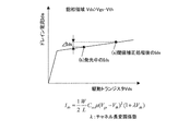
[実施例1]
図1および図2に示すシステム構成の有機EL表示装置10において、実施例1に係る電源供給走査回路50は、電源供給線32の電位DSとして3値の電位を設定可能な構成となっている。具体的には、実施例1に係る電源供給走査回路50は、高電位Vccp(以下、Vccp1と記述する)と、低電位Viniと、それらの間の中間電位Vccp2との3値の電位を電源電位DSとして適宜設定できるようになっている。
[Example 1]
In the organic EL display device 10 having the system configuration shown in FIGS. 1 and 2, the power
実施例1に係る電源電位DSの設定についてのタイミング関係を図13に示す。電源供給走査回路50は、閾値補正準備期間(t11−t13)では低電位Viniを設定し、少なくとも閾値補正期間(t13−t14)では中間電位Vccp2を設定し、発光期間(t17以降)では高電位Vccp1を設定する。
FIG. 13 shows the timing relationship for setting the power supply potential DS according to the first embodiment. The power
すなわち、先述した基本的な回路動作の場合、電源供給線32の電位DSを閾値補正期間と発光期間とで同じ高電位Vccp1(Vccp)に設定するようにしていた。これに対して、本実施例1では、電源供給線32の電位DSを閾値補正期間と発光期間とで異ならせる、具体的には、閾値補正期間で中間電位Vccp2(<Vccp1)に設定し、発光期間で高電位Vccp1に設定するようにしている。
That is, in the basic circuit operation described above, the potential DS of the
先述したように、電源供給線32の電位DSが閾値補正期間と発光期間とで同じだと、閾値補正処理後と有機EL素子21の発光中とで駆動トランジスタ22のドレイン−ソース間電圧Vdsに違いが生じる。
As described above, when the potential DS of the
そこで、本実施例1においては、電源供給線32の電位DSを閾値補正期間と発光期間とで異ならせる構成を採っている。これにより、閾値補正処理後のドレイン−ソース間電圧Vds(a)と有機EL素子21の発光中のドレイン−ソース間電圧Vds(b)との違いを、電源供給線32の電位DSが閾値補正期間と発光期間とで同じ場合に比べて小さくできる。その結果、駆動トランジスタ22にキンク現象が発生し、その発生状態に製造ばらつきによってばらつきが生じたとしても、画素間での駆動トランジスタ22のドレイン−ソース間電流Idsのばらつきを小さく抑えることができる。
Therefore, the first embodiment employs a configuration in which the potential DS of the
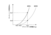
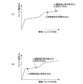
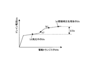
ここで、閾値補正期間で設定する中間電位Vccp2については、発光期間で設定する高電位Vccp1に対して次のように設定するのが好ましい。すなわち、閾値補正処理後の駆動トランジスタ22のドレイン−ソース間電圧Vds(a)と有機EL素子21の発光中の駆動トランジスタ22のドレイン−ソース間電圧Vds(b)とが等しくなるような電位に中間電位Vccp2を設定するのが好ましい。
Here, the intermediate potential Vccp2 set in the threshold correction period is preferably set as follows with respect to the high potential Vccp1 set in the light emission period. That is, the drain-source voltage Vds (a) of the
図14には、駆動トランジスタ22の特性が、理想的なトランジスタ特性の場合のVds−Ids特性を示している。図15には、駆動トランジスタ22の特性が、キンク現象が発生するトランジスタ特性の場合のVds−Ids特性を示している。
FIG. 14 shows Vds-Ids characteristics when the characteristics of the
このような電位関係にて高電位Vccp1に対して中間電位Vccp2を設定することで、キンク現象に起因する画素間での駆動トランジスタ22のドレイン−ソース間電流Idsのばらつきをより小さく抑えることができる(理想的にはばらつきを無くすことができる)。その結果、表示画像の画質を改善できる。
By setting the intermediate potential Vccp2 with respect to the high potential Vccp1 in such a potential relationship, the variation in the drain-source current Ids of the
(電源供給回路)
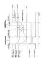
ここで、電源供給線32の電源電位DSとして、3値の電位Vccp1,Vccp2,Viniを設定可能な電源供給走査回路50Aの具体的な構成について説明する。
(Power supply circuit)
Here, a specific configuration of the power supply scanning circuit 50A capable of setting ternary potentials Vccp1, Vccp2, and Vini as the power supply potential DS of the
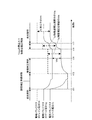
図16は、3値の電位Vccp1,Vccp2,Viniを設定可能な電源供給走査回路50Aの構成の一例を示すブロック図である。 FIG. 16 is a block diagram showing an example of the configuration of a power supply scanning circuit 50A capable of setting ternary potentials Vccp1, Vccp2, and Vini.
電源供給走査回路50Aは、シフトレジスタ51と波形整形論理回路52とから構成されている。シフトレジスタ51は、書込み走査回路40(図1参照)による垂直走査に同期して、2つのタイミング信号T1,T2を画素行ごとに出力する。波形整形論理回路52は、2つのタイミング信号T1,T2に基づいて3値の電位Vccp1,Vccp2,Viniを適宜出力する。
The power supply scanning circuit 50A includes a
図17は、波形整形論理回路52の構成の一例を示す回路図である。本例に係る波形整形論理回路52は、2つのNAND回路521,522と、2つのインバータ523,524と、2つのPchMOSトランジスタ525,526と、1つのNchMOSトランジスタ527とから構成されている。
FIG. 17 is a circuit diagram showing an example of the configuration of the waveform
NAND回路521は、入力端子in1を介して入力されるタイミング信号T1を一方の入力とし、入力端子in2を介して入力され、インバータ524で論理反転されるタイミング信号T2を他方の入力とする。NANAD回路522は、入力端子in1を介して入力され、インバータ523で論理反転されるタイミング信号T1を一方の入力とし、入力端子in2を介して入力され、インバータ524で論理反転されるタイミング信号T2を他方の入力とする。
The
PchMOSトランジスタ525は、NAND回路521の出力をゲート入力とし、当該出力がLowレベルのときに導通状態となって電源電位VDD1を高電位Vccp1として出力端子outを通して出力する。PchMOSトランジスタ526は、NAND回路522の出力をゲート入力とし、当該出力がLowレベルのときに導通状態となって電源電位VDD2を中間電位Vccp2として出力端子outを通して出力する。NchMOSトランジスタ527は、タイミング信号T2をゲート入力とし、当該タイミング信号T2がHighレベルのときに導通状態となって電源電位VSSを低電位Viniとして出力端子outを通して出力する。
The
図18に、タイミング信号T1,T2のタイミング関係を示す。このタイミング波形図に示すように、閾値補正準備期間でタイミング信号T1がLowレベルに、タイミング信号T2がHighレベルになることで、電源供給走査回路50Aから低電位Viniが出力される。閾値補正期間から発光期間に入る前までの期間でタイミング信号T1,T2が共にLowレベルになることで、電源供給走査回路50Aから中間電位Vccp2が出力される。発光期間でタイミング信号T1がHighレベルに、タイミング信号T2がLowレベルになることで、電源供給走査回路50Aから高電位Vccp1が出力される。 FIG. 18 shows the timing relationship between the timing signals T1 and T2. As shown in the timing waveform diagram, the low potential Vini is output from the power supply scanning circuit 50A when the timing signal T1 becomes Low level and the timing signal T2 becomes High level in the threshold correction preparation period. Since both the timing signals T1 and T2 are at the low level during the period from the threshold correction period to before the light emission period, the intermediate potential Vccp2 is output from the power supply scanning circuit 50A. When the timing signal T1 becomes High level and the timing signal T2 becomes Low level in the light emission period, the high potential Vccp1 is output from the power supply scanning circuit 50A.
(Vccp1,Vccp2の設定)
先述したように、本実施例1においては、中間電位Vccp2を高電位Vccp1に対して、好ましくは、閾値補正処理後の駆動トランジスタ22のドレイン−ソース間電圧Vds(a)と有機EL素子21の発光中の駆動トランジスタのドレイン−ソース間電圧Vds(b)とが等しくなるように設定する。このとき、信号書込み+移動度補正期間での電源供給線32の電位DSを、閾値補正期間と同じ中間電位Vccp2に設定している。
(Setting of Vccp1 and Vccp2)
As described above, in the first embodiment, the intermediate potential Vccp2 is set higher than the high potential Vccp1, and the drain-source voltage Vds (a) of the
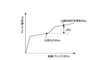
しかし、移動度補正期間の電位DSを中間電位Vccp2とした場合、移動度補正期間中の駆動トランジスタ22のドレイン−ソース間電圧Vds(c)が、閾値補正処理後および発光中のドレイン−ソース間電圧Vds(a),(b)よりも小さくなる(図13参照)。これにより、図19に示すように、駆動トランジスタ22をキンク現象が発生する領域(以下、「キンク現象の領域」と記述する)で使用してしまう可能性がある。キンク現象の領域で使用すると、それ以外の領域で使用する場合よりも、画素間において駆動トランジスタ22のドレイン−ソース間電流Idsにばらつきが発生し易くなるために、画素間において輝度差が発生する。
However, when the potential DS in the mobility correction period is set to the intermediate potential Vccp2, the drain-source voltage Vds (c) of the
このような理由から、中間電位Vccp2のみならず、高電位Vccp1についても、移動度補正期間において駆動トランジスタ22をキンク現象の領域で使用しないように各電位を設定することが望ましい。具体的には、出荷前において、移動度補正期間において駆動トランジスタ22をキンク現象の領域で使用している場合は、そのときの電位よりも電位Vccp1,Vccp2の各電位を上げるか、または下げる。
For this reason, not only the intermediate potential Vccp2 but also the high potential Vccp1 is desirably set so that the
電位Vccp1,Vccp2の各電位を上げることで図20(A)に示すように、下げることで図20(B)に示すように、駆動トランジスタ22をキンク現象の領域で使用しないようにすることができる。その結果、キンク現象が存在するトランジスタ特性においても、画素間における駆動トランジスタ22のドレイン−ソース間電流Idsのばらつきを抑制することができるため、表示画像の画質を改善できる。
As shown in FIG. 20A, the potentials Vccp1 and Vccp2 are increased, and as shown in FIG. 20B, the
[実施例2]
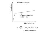
図1および図2に示すシステム構成の有機EL表示装置10において、実施例2に係る電源供給走査回路50は、電源供給線32の電位DSとして、4値の電位を設定可能な構成となっている。具体的には、電源供給走査回路50は、高電位Vccp1と、低電位Viniと、それらの間の中間電位Vccp2,Vccp3との4値の電位を電源電位DSとして適宜設定できるようになっている。ここで、中間電位Vccp2,Vccp3は、Vccp2<Vccp3の高低関係にある。
[Example 2]
In the organic EL display device 10 having the system configuration shown in FIGS. 1 and 2, the power
実施例1では、移動度補正期間(信号電圧Vsigの書込み期間を含む)での電源供給線32の電位DSを中間電位Vccp2に設定していた。すなわち、移動度補正期間における電源供給線32の電位DSを閾値補正期間と移動度補正期間とで同じ電位に設定していた。これに対して、実施例2では、移動度補正期間における電源供給線32の電位DSを閾値補正期間と移動度補正期間とで異なる中間電位Vccp2,Vccp3に設定することを特徴としている。
In the first embodiment, the potential DS of the
実施例2に係る電源電位DSの設定についてのタイミング関係を図21に示す。電源供給走査回路50は、閾値補正準備期間(t11−t13)では低電位Viniを設定し、少なくとも閾値補正期間(t13−t14)では中間電位Vccp2を設定する。電源供給走査回路50はさらに、信号書込み+移動度補正期間(t16−t17)では中間電位Vccp3を設定し、発光期間(t17以降)では高電位Vccp1を設定する。
FIG. 21 shows the timing relationship for setting the power supply potential DS according to the second embodiment. The power
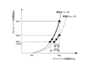
すなわち、実施例1では、移動度補正期間における電源供給線32の電位DSを閾値補正期間と移動度補正期間とで同じ中間電位Vccp2に設定するようにしていた。これに対して、本実施例2では、電源供給線32の電位DSを閾値補正期間と移動度期間とで異ならせる、具体的には、閾値補正期間で中間電位Vccp2に設定し、移動度期間で中間電位Vccp3に設定するようにしている。
That is, in the first embodiment, the potential DS of the
電源供給線32の電位DSが閾値補正期間と発光期間とで異なっていたとしても、先述したように、移動度補正期間における電源供給線32の電位DSを閾値補正期間と移動度補正期間とで同じ中間電位Vccp2とした場合、駆動トランジスタ22をキンク現象の領域で使用してしまう可能性がある。その結果、画素間において駆動トランジスタ22のドレイン−ソース間電流Idsにばらつきが発生し易くなるために、画素間において輝度差が発生する。
Even if the potential DS of the
これに対して、電源供給線32の電位DSを閾値補正期間と移動度期間とで異ならせることで、たとえ駆動トランジスタ22をキンク現象の領域で使用していても、画素間での駆動トランジスタ22のドレイン−ソース間電流Idsのばらつきを小さく抑えることができる。ここで、中間電位Vccp3については中間電位Vccp2に対して、閾値補正処理後のドレイン−ソース間電圧Vds(a)と、移動度補正中の駆動トランジスタ22のドレイン−ソース間電圧Vds(c)とが等しくなるような電位に設定するのが好ましい。
On the other hand, by making the potential DS of the
このような電位関係にて中間電位Vccp2に対して中間電位Vccp3を設定することで、図22に示すように、閾値補正処理後、移動度補正処理後および発光期間を全て同じドレイン−ソース間電圧Vdsとすることができる。これにより、たとえ駆動トランジスタ22をキンク現象の領域で使用していても、閾値補正および移動度補正の各処理の終わりと発光中でドレイン−ソース間電圧Vdsが変動しない。その結果、キンク現象に起因する画素間での駆動トランジスタ22のドレイン−ソース間電流Idsのばらつきをより小さく抑えることができる(理想的にはばらつきを無くすことができる)ため、表示画像の画質を改善できる。
By setting the intermediate potential Vccp3 with respect to the intermediate potential Vccp2 in such a potential relationship, the drain-source voltage is all the same after the threshold correction processing, after the mobility correction processing, and during the light emission period as shown in FIG. Vds can be used. Thereby, even if the driving
(電源供給回路)
ここで、電源供給線32の電源電位DSとして、4値の電位Vccp1,Vccp2,Vccp3,Viniを設定可能な電源供給走査回路50Bの具体的な構成について説明する。
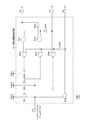
(Power supply circuit)
Here, a specific configuration of the power supply scanning circuit 50B capable of setting quaternary potentials Vccp1, Vccp2, Vccp3, and Vini as the power supply potential DS of the
図23は、4値の電位Vccp1,Vccp2,Vccp3,Viniを設定可能な電源供給走査回路50Bの構成の一例を示すブロック図である。 FIG. 23 is a block diagram showing an example of the configuration of a power supply scanning circuit 50B capable of setting four-level potentials Vccp1, Vccp2, Vccp3, and Vini.
電源供給走査回路50Bは、シフトレジスタ53と波形整形論理回路54とから構成されている。シフトレジスタ53は、書込み走査回路40(図1参照)による垂直走査に同期して、3つのタイミング信号T1,T2,T3を画素行ごとに出力する。波形整形論理回路54は、3つのタイミング信号T1,T2,T3に基づいて4値の電位Vccp1,Vccp2,Vccp3,Viniを適宜出力する。 The power supply scanning circuit 50B includes a shift register 53 and a waveform shaping logic circuit 54. The shift register 53 outputs three timing signals T1, T2, and T3 for each pixel row in synchronization with the vertical scanning by the writing scanning circuit 40 (see FIG. 1). The waveform shaping logic circuit 54 appropriately outputs quaternary potentials Vccp1, Vccp2, Vccp3, and Vini based on the three timing signals T1, T2, and T3.
図24は、波形整形論理回路54の構成の一例を示す回路図である。本例に係る波形整形論理回路54は、2つのAND回路541,542と、3つのインバータ543〜545と、3つのNAND回路546〜548と、3つのPchMOSトランジスタ549〜551と、1つのNchMOSトランジスタ552とから構成されている。
FIG. 24 is a circuit diagram showing an example of the configuration of the waveform shaping logic circuit 54. The waveform shaping logic circuit 54 according to this example includes two AND
AND回路541は、入力端子in1を介して入力されるタイミング信号T1を一方の入力とし、入力端子in2を介して入力され、インバータ544で論理反転されるタイミング信号T2を他方の入力とする。ANAD回路542は、入力端子in1を介して入力され、インバータ543で論理反転されるタイミング信号T1を一方の入力とし、入力端子in2を介して入力され、インバータ544で論理反転されるタイミング信号T2を他方の入力とする。
The AND
NAND回路546はAND回路541の出力を一方の入力とする。NAND回路547はAND回路542の出力を一方の入力とする。NAND回路548は入力端子in2を介して入力されるタイミング信号T3を一方の入力とする。NAND回路546〜548は、入力端子in3を介して入力され、インバータ545で論理反転されるタイミング信号T3を各他方の入力とする。
The
PchMOSトランジスタ549は、NAND回路546の出力をゲート入力とし、当該出力がLowレベルのときに導通状態となって電源電位VDD1を高電位Vccp1として出力端子outを通して出力する。PchMOSトランジスタ550は、NAND回路547の出力をゲート入力とし、当該出力がLowレベルのときに導通状態となって電源電位VDD2を中間電位Vccp2として出力端子outを通して出力する。
The
PchMOSトランジスタ551は、NAND回路548の出力をゲート入力とし、当該出力がLowレベルのときに導通状態となって電源電位VDD3を中間電位Vccp3として出力端子outを通して出力する。NchMOSトランジスタ552は、タイミング信号T3をゲート入力とし、当該タイミング信号T3がHighレベルのときに導通状態となって電源電位VSSを低電位Viniとして出力端子outを通して出力する。
The
図25に、タイミング信号T1,T2,T3のタイミング関係を示す。このタイミング波形図に示すように、閾値補正準備期間でタイミング信号T1,T2が共にLowレベルに、タイミング信号T3がHighレベルになることで、電源供給走査回路50Bから低電位Viniが出力される。閾値補正期間から発光期間に入る前までの期間でタイミング信号T1,T3が共にLowレベルに、タイミング信号T2がHighレベルになることで、電源供給走査回路50Bから中間電位Vccp2が出力される。 FIG. 25 shows the timing relationship between the timing signals T1, T2, and T3. As shown in the timing waveform diagram, in the threshold correction preparation period, the timing signals T1 and T2 are both set to the low level, and the timing signal T3 is set to the high level, so that the low potential Vini is output from the power supply scanning circuit 50B. In the period from the threshold correction period to before the light emission period, the timing signals T1 and T3 are both set to the low level, and the timing signal T2 is set to the high level, whereby the intermediate potential Vccp2 is output from the power supply scanning circuit 50B.
信号書込み+移動度補正期間でタイミング信号T1,T2,T3が共にLowレベルになることで、電源供給走査回路50Bから中間電位Vccp3が出力される。また、発光期間でタイミング信号T1がHighレベルに、タイミング信号T2,T3が共にLowレベルになることで、電源供給走査回路50Bから高電位Vccp1が出力される。
Since the timing signals T1, T2, and T3 are all at the low level in the signal writing + mobility correction period, the intermediate potential Vccp3 is output from the power supply scanning circuit 50B. Further, the timing signal T1 is set to the high level and the timing signals T2 and T3 are both set to the low level during the light emission period, so that the high potential Vccp1 is output from the power supply scanning circuit 50B.
<3.第2実施形態>
本発明の第2実施形態に係る有機EL表示装置10Bは、信号出力回路60が映像信号の信号電圧Vsigと、基準電位Vofsと、少なくとも1種類の中間階調電圧Vmidとを選択的に出力する構成となっている。
<3. Second Embodiment>
In the organic EL display device 10B according to the second embodiment of the present invention, the
ここで、基準電位Vofsは、第1実施形態の場合と同様に、映像信号の信号電圧Vsigの基準となる電位であり、閾値補正処理の際の駆動トランジスタ22のゲート電位Vgの初期化電位として用いられる。中間階調電圧Vmidは、駆動トランジスタ22のゲート電位Vgの初期化電位となる基準電位Vofsと、信号電圧Vsigの最大電圧、即ち白階調の信号電圧Vsig(W)との間の電圧であり、後述するように、移動度補正処理を複数回行うために用いられる。
Here, as in the case of the first embodiment, the reference potential Vofs is a potential serving as a reference for the signal voltage Vsig of the video signal, and is used as an initialization potential of the gate potential Vg of the
[回路動作]
続いて、第2実施形態に係る有機EL表示装置10Bの基本的な回路動作について、図26のタイミング波形図を基に図27および図28の動作説明図を用いて説明する。なお、図27および図28の動作説明図では、図面の簡略化のために、書込みトランジスタ23をスイッチのシンボルで図示している。また、有機EL素子21の等価容量25についても図示している。
[Circuit operation]
Subsequently, the basic circuit operation of the organic EL display device 10B according to the second embodiment will be described with reference to the operation explanatory diagrams of FIGS. 27 and 28 based on the timing waveform diagram of FIG. In the operation explanatory diagrams of FIGS. 27 and 28, the
図26のタイミング波形図には、走査線31の電位(書込み走査信号)WS、電源供給線32の電位(電源電位)DS、信号線33の電位(Vsig/Vofs/Vmid)、駆動トランジスタ22のゲート電位Vgおよびソース電位Vsのそれぞれの変化を示している。 In the timing waveform diagram of FIG. 26, the potential of the scanning line 31 (write scanning signal) WS, the potential of the power supply line 32 (power supply potential) DS, the potential of the signal line 33 (Vsig / Vofs / Vmid), Changes in the gate potential Vg and the source potential Vs are shown.
先述した第1実施形態に係る有機EL表示装置10Aの基本的な回路動作では、閾値補正処理を1回だけ実行する駆動法を採る場合を例に挙げて説明した。これに対して、本実施形態に係る有機EL表示装置10Bの基本的な回路動作では、分割Vth補正を行う駆動法を採るものとする。ただし、閾値補正処理を1回だけ実行する駆動法を採っても良いことは勿論である。 In the basic circuit operation of the organic EL display device 10A according to the first embodiment described above, the case where the driving method in which the threshold correction process is executed only once is taken as an example. On the other hand, in the basic circuit operation of the organic EL display device 10B according to the present embodiment, a driving method for performing divided Vth correction is adopted. However, it goes without saying that a driving method in which the threshold correction process is executed only once may be adopted.
(前フレームの発光期間)
図26のタイミング波形図において、時刻t21以前は、前のフレームにおける有機EL素子21の発光期間となる。この前フレームの発光期間では、電源供給線32の電位DSが高電位Vccpにある。また、書込みトランジスタ23が非導通状態にある。
(Prior frame emission period)
In the timing waveform diagram of FIG. 26, the time before time t21 is the light emission period of the
このとき、駆動トランジスタ22は飽和領域で動作するように設計されている。これにより、図27(A)に示すように、駆動トランジスタ22のゲート−ソース間電圧Vgsに応じた駆動電流(ドレイン−ソース間電流)Idsが、電源供給線32から駆動トランジスタ22を通して有機EL素子21に供給される。よって、有機EL素子21が駆動電流Idsの電流値に応じた輝度で発光する。
At this time, the
(閾値補正準備)
時刻t21になると、線順次走査の新しいフレーム(現フレーム)に入る。そして、図27(B)に示すように、電源供給線32の電位DSが高電位Vccpから低電位Viniに切り替わる。このとき、低電位Viniが有機EL素子21の閾値電圧Vthelとカソード電位Vcathの和よりも小さければ、即ちVini<Vthel+Vcathであれば有機EL素子21は逆バイアス状態となる。したがって、有機EL素子21は消光する。このとき、有機EL素子21のアノード電位は低電位Viniなる。
(Threshold correction preparation)
At time t21, a new frame (current frame) for line sequential scanning is entered. Then, as shown in FIG. 27B, the potential DS of the
次に、信号線33の電位が基準電位Vofsにある時刻t22で走査線31の電位WSが低電位側から高電位側に遷移することで、図27(C)に示すように、書込みトランジスタ23が導通状態となる。このとき、駆動トランジスタ22のゲート電圧Vgが基準電位Vofsになるため、駆動トランジスタ22のゲート−ソース間電圧VgsはVofs−Viniとなる。
Next, at time t22 when the potential of the
ここで、Vofs−Viniが駆動トランジスタ22の閾値電圧Vthよりも大きくないと、閾値補正処理を行うことができないために、Vofs−Vini>Vthなる電位関係に設定する必要がある。
Here, unless Vofs−Vini is larger than the threshold voltage Vth of the
このようにして、駆動トランジスタ22のゲート電圧Vgを基準電位Vofsに、ソース電圧Vsを低電位Viniにそれぞれ初期化させる閾値補正準備の処理が行なわれる。この閾値補正準備の処理は、走査線31の電位WSが高電位にある時刻t22から時刻t23までの期間(閾値補正準備期間)において行われる。
In this way, threshold correction preparation processing is performed to initialize the gate voltage Vg of the
(分割Vth補正)
次に、時刻t24で走査線31の電位WSが低電位側から高電位側に遷移することで、書込みトランジスタ23が再び導通状態となる。そして、時刻t25で電源供給線32の電位DSが低電位Viniから高電位Vccpに切り替わると、図27(D)に示すように、電源供給線32→駆動トランジスタ22→有機EL素子21のアノード→保持容量24の経路で電流が流れる。
(Division Vth correction)
Next, at time t24, the potential WS of the scanning line 31 transitions from the low potential side to the high potential side, so that the writing
ここで、有機EL素子21はダイオードと容量(等価容量)で表わされるために、有機EL素子21のアノード電圧VelがVel≦Vcath+Vthelである限り、駆動トランジスタ22を流れる電流は保持容量24と等価容量Celの充電に使われる。ここで、Vel≦Vcath+Vthelということは、有機EL素子21のリーク電流が駆動トランジスタ22を流れる電流よりもかなり小さいということである。
Here, since the
この充電動作により、有機EL素子21のアノード電圧Vel、即ち駆動トランジスタ22のソース電圧Vsは、図29に示すように、時間の経過とともに上昇してゆく。すなわち、駆動トランジスタ22のゲート電極の初期化電位Vofsを基準として、当該初期化電位Vofsから駆動トランジスタ22の閾値電圧Vthを減じた電位に向けてソース電圧Vsを変化させる閾値補正処理が行われる。
As a result of this charging operation, the anode voltage Vel of the
時刻t25から一定時間が経過した時刻t26で、走査線31の電位WSが高電位側から低電位側に遷移することで、書込みトランジスタ23が非導通状態となる。この時刻t25から時刻t26までの期間が1回目の閾値補正期間となる。
At time t26 when a certain time has elapsed from time t25, the potential WS of the scanning line 31 transitions from the high potential side to the low potential side, so that the writing
この閾値補正期間では、駆動トランジスタ22のゲート−ソース間電圧Vgsが閾値電圧Vthよりも大きいために、図28(A)に示すように、電源供給線32→駆動トランジスタ22→有機EL素子21のアノード→保持容量24の経路で電流が流れる。これにより、駆動トランジスタ22のゲート電圧Vgおよびソース電圧Vsが上昇してゆく。このとき、有機EL素子21には逆バイアスがかかっているために当該有機EL素子21が発光することはない。
In this threshold correction period, since the gate-source voltage Vgs of the driving
そして再び信号線33の電位が基準電位Vofsにある時刻27で走査線31の電位WSが低電位側から高電位側に遷移することで、書込みトランジスタ23が再び導通状態となる。これにより、駆動トランジスタ22のゲート電圧Vgが基準電位Vofsに初期化され、2回目の閾値補正処理が開始される。この2回目の閾値補正処理は、時刻t28で走査線31の電位WSが高電位側から低電位側に遷移し、書込みトランジスタ23が非導通状態になるまで行われる。
Then, at time 27 when the potential of the
以降、時刻t29から時刻t30までの期間で3回目の閾値補正処理が行われる。本回路動作例では、閾値補正処理を3H期間に亘って3分割して行うとしているが、これは一例に過ぎず、分割Vth補正としては3分割に限られるものではない。 Thereafter, the third threshold correction process is performed in the period from time t29 to time t30. In this circuit operation example, the threshold correction processing is performed by dividing it into three over a 3H period. However, this is only an example, and the divided Vth correction is not limited to three.
この分割Vth補正の処理動作を繰り返すことで、駆動トランジスタ22のゲート−スース間電圧Vgsは、最終的に、駆動トランジスタ22の閾値電圧Vthに収束する。この閾値電圧Vthに相当する電圧は保持容量24に保持される。
By repeating this divided Vth correction processing operation, the gate-source voltage Vgs of the
なお、閾値補正処理において、電流が専ら保持容量24側に流れ、有機EL素子21側には流れないようにする必要がある。そのために、有機EL素子21がカットオフ状態となるように共通電源供給線34の電位Vcathを設定しておくこととする。
In the threshold correction process, it is necessary to prevent current from flowing exclusively to the
時刻t30で走査線31の電位WSが高電位側から低電位側に遷移することで、書込みトランジスタ23が非導通状態となる。このとき、駆動トランジスタ22のゲート電極が信号線33から電気的に切り離されることによってフローティング状態になる。しかし、ゲート−ソース間電圧Vgsが駆動トランジスタ22の閾値電圧Vthに等しいために、当該駆動トランジスタ22はカットオフ状態にある。したがって、駆動トランジスタ22にドレイン−ソース間電流Idsは流れない。
At time t30, the potential WS of the scanning line 31 transitions from the high potential side to the low potential side, so that the writing
3回目の閾値補正処理の終了後、信号出力回路60から信号線33に対して基準電位Vofsに代えて中間階調電圧Vmidが出力される。すなわち、信号線33の電位が基準電位Vofsから中間階調電圧Vmidに切り替わる。この中間階調電圧Vmidは、映像信号の信号電圧Vsigの書込み前に、1回目の移動度補正処理を実行させるための電圧である。
After the completion of the third threshold correction process, the
(移動度補正1)
次に、信号線33の電位が中間階調電圧Vmidにある時刻t31で走査線31の電位WSが低電位側から高電位側に遷移することで、図28(B)に示すように、書込みトランジスタ23が再び導通状態となる。これにより、中間階調電圧Vmidが画素内に書き込まれ、2段階の移動度補正処理の1段階目(1回目)の移動度補正処理が行われる。
(Mobility correction 1)
Next, at time t31 when the potential of the
この1段階目の移動度補正処理の期間は、信号線33の電位が中間階調電圧Vmidから映像信号の信号電圧Vsigに切り替わる時刻t32までの期間となる。中間階調電圧Vmidを用いて1回目の移動度補正処理を実行することによる作用効果の詳細については後述する。
This first-stage mobility correction processing period is a period from time t32 when the potential of the
(信号書込み+移動度補正2)
次に、書込みトランジスタ23が導通状態にある時刻t32で信号線33の電位が中間階調電圧Vmidから映像信号の信号電圧Vsigに切り替わることで、当該信号電圧Vsigが画素内に書き込まれる。これにより、図28(C)に示すように、駆動トランジスタ22のゲート電位Vgが中間階調電圧Vmidから映像信号の信号電圧Vsigへと変化する。
(Signal writing + mobility correction 2)
Next, the potential of the
すなわち、書込みトランジスタ23によって映像信号の信号電圧Vsigが書き込まれることで、駆動トランジスタ22のゲート電圧Vgが信号電圧Vsigとなる。そして、映像信号の信号電圧Vsigによる駆動トランジスタ22の駆動の際に、当該駆動トランジスタ22の閾値電圧Vthが保持容量24に保持されている閾値電圧Vthに相当する電圧とキャンセルされる。
That is, the signal voltage Vsig of the video signal is written by the writing
一方、駆動トランジスタ22のソース電位Vsは、電源供給線32から駆動トランジスタ22を通して電流が流れるために時間の経過とともに上昇してゆく。このとき、駆動トランジスタ22のソース電位Vsが有機EL素子21の閾値電圧Vthelとカソード電位Vcathの和を越えなければ、駆動トランジスタ22に流れる電流(ドレイン−ソース間電流Ids)は、保持容量24と有機EL素子21の等価容量25を充電するのに使用される。
On the other hand, the source potential Vs of the driving
このとき既に、駆動トランジスタ22の閾値電圧Vthの画素ごとのばらつきがキャンセルされているために、駆動トランジスタ22に流れる電流は当該駆動トランジスタ22の移動度μを反映したものとなる。具体的に言うと、図30に示すように、移動度μが大きい駆動トランジスタ22の場合は、このときの電流量が大きく、ソース電位Vsの上昇が早くなる。逆に、移動度μが小さい駆動トランジスタ22の場合は、電流量が小さく、ソース電位Vsの上昇が遅くなる。
At this time, since the variation of the threshold voltage Vth of the
したがって、駆動トランジスタ22に流れる電流に応じた帰還量ΔVでゲート‐ソース間電圧Vgsに負帰還をかけることで、駆動トランジスタ22のドレイン−ソース間電流Idsの移動度μに対する依存性を打ち消すことができる。すなわち、第1実施形態の回路動作でも詳しく述べたように、当該負帰還によって移動度μの画素ごとのばらつきを補正することができる。この2回目の移動度補正処理は、信号電圧Vsigの書込み処理と並行して行われる。
Therefore, by applying negative feedback to the gate-source voltage Vgs with a feedback amount ΔV corresponding to the current flowing through the
(発光期間)
次に、時刻t33で走査線31の電位WSが低電位側に遷移することで、図28(D)に示すように、書込みトランジスタ23が非導通状態となる。これにより、駆動トランジスタ22のゲート電極は、信号線33から電気的に切り離されるためにフローティング状態になる。
(Light emission period)
Next, at time t33, the potential WS of the scanning line 31 transitions to the low potential side, so that the writing
駆動トランジスタ22のゲート電極がフローティング状態になると同時に、駆動トランジスタ22のドレイン−ソース間電流Idsが有機EL素子21に流れ始めることで、当該電流Idsに応じて有機EL素子21のアノード電位が上昇する。そして、有機EL素子21のアノード電位がVthel+Vcathを越えると、有機EL素子21に駆動電流が流れ始めるため有機EL素子21が発光を開始する。
At the same time that the gate electrode of the driving
本実施形態に係る有機EL表示装置10Bにおいても、有機EL素子21の発光時間が長くなると、当該有機EL素子21のI−V特性が変化してしまう。そのため、駆動トランジスタ22のソース電位Vsも変化する。しかしながら、駆動トランジスタ22のゲート−ソース間電圧Vgsが一定に保たれているために、有機EL素子21に流れる電流は
変化しない。よって、有機EL素子21のI−V特性が劣化しても、有機EL素子21に一定電流が流れ続けるために、有機EL素子21の発光輝度が変化することはない。
Also in the organic EL display device 10 </ b> B according to the present embodiment, when the light emission time of the
[2回の移動度補正に伴う作用効果]
ところで、最適な移動度補正時間tは、
t=C/(kμVsig) ……(4)
なる式で与えられる。ここで、定数kはk=(1/2)(W/L)Coxである。また、Cは移動度補正を行うときに放電されるノードの容量であり、図2の回路例では有機EL素子21の等価容量、保持容量24および駆動トランジスタ22のゲート−ソース間の寄生容量等の合成容量となる。
[Effects of two mobility corrections]
By the way, the optimum mobility correction time t is
t = C / (kμVsig) (4)
It is given by Here, the constant k is k = (1/2) (W / L) Cox. Further, C is a capacitance of a node that is discharged when the mobility correction is performed. In the circuit example of FIG. The combined capacity of
上記式(4)から明らかなように、移動度補正時間tは、映像信号の信号電圧Vsigに対して反比例の関係にある。この点に鑑み、第1実施形態に係る有機EL表示装置10Aでは、図4のタイミング波形図における時刻t17の走査線電位(書込み走査信号)WSの立ち下がり波形が、映像信号の信号電圧Vsigの大きさに対して反比例する波形になるように設定している。因みに、第1実施形態の説明では、書込み走査信号WSの立ち下がり波形についての詳細な説明については割愛している。 As is apparent from the above equation (4), the mobility correction time t is inversely proportional to the signal voltage Vsig of the video signal. In view of this point, in the organic EL display device 10A according to the first embodiment, the falling waveform of the scanning line potential (write scanning signal) WS at time t17 in the timing waveform diagram of FIG. 4 is the signal voltage Vsig of the video signal. The waveform is set to be inversely proportional to the size. Incidentally, in the description of the first embodiment, a detailed description of the falling waveform of the write scanning signal WS is omitted.
信号書込み終了時の書込み走査信号WSの立ち下がり波形を、信号電圧Vsigの大きさに反比例するように設定することにより、書込みトランジスタ23のゲート−ソース間電圧が閾値電圧Vthになったところで当該書込みトランジスタ23がカットオフする。したがって、移動度補正時間tを映像信号の信号電圧Vsigの大きさに反比例するように設定できる。
By setting the falling waveform of the write scanning signal WS at the end of signal writing to be inversely proportional to the magnitude of the signal voltage Vsig, the write operation is performed when the gate-source voltage of the
具体的には、白レベルに対応した信号電圧Vsig(白)のときは、書込みトランジスタ23はゲート−ソース間電圧がVsig(白)+Vthになったところでカットオフする。したがって、白表示時の移動度補正時間t(白)が一番短く設定される。また、グレーレベルに対応した信号電圧Vsig(グレー)のときは、書込みトランジスタ23はゲート−ソース間電圧がVsig(グレー)+Vthになったところでカットオフする。したがって、グレー表示時の移動度補正時間t(グレー)が移動度補正時間t(白)よりも長く設定される。
Specifically, when the signal voltage Vsig (white) corresponds to the white level, the writing
このように、第1実施形態に係る有機EL表示装置10Aでは、信号書込み終了時の書込み走査信号WSの立ち下がり波形を、信号電圧Vsigの大きさに反比例するように設定することで、最適な移動度補正時間tを設定するようにしている。これにより、最適な移動度補正時間tを信号電圧Vsigの大きさに対応して設定できるために、全階調に亘って駆動トランジスタ22の移動度μの画素ごとのばらつきをより確実に補正することができる。
Thus, in the organic EL display device 10A according to the first embodiment, the falling waveform of the write scanning signal WS at the end of signal writing is set so as to be inversely proportional to the magnitude of the signal voltage Vsig. The mobility correction time t is set. Thus, since the optimum mobility correction time t can be set corresponding to the magnitude of the signal voltage Vsig, the variation of the mobility μ of the
ここで、移動度補正時間tを決める書込み走査信号WSは、図1に示す書込み走査回路40において走査段ごとに生成される。そして、信号書込み終了時の書込み走査信号WSの立ち下がり波形を、信号電圧Vsigの大きさに反比例するように設定するには、書込み走査回路40の回路構成が複雑化する。これは、表示装置全体のコストアップの一因となる。
Here, the writing scanning signal WS for determining the mobility correction time t is generated for each scanning stage in the
また、書込み走査信号WSの立ち下がり波形に各走査段ごとに波形ばらつきが生じると、特に移動度補正時間tが短い白レベル側でそのばらつきの影響を受け易くなる。すなわち、書込み走査信号WSの立ち下がり波形にばらつきが生じると、特に白表示時に移動度補正時間t(白)が走査段ごとにばらつくために、移動度補正にばらつきが生じ、各走査段で最適な移動度補正を実行できないことになる。 In addition, when the falling waveform of the writing scanning signal WS has a waveform variation for each scanning stage, the waveform is likely to be affected by the variation particularly on the white level side where the mobility correction time t is short. In other words, if the falling waveform of the write scanning signal WS varies, the mobility correction time t (white) varies especially from scanning stage to white stage when white is displayed. Therefore, it is impossible to perform the mobility correction.
このような観点がすると、移動度補正時間tが一定でありながら、信号電圧Vsigの全レベル範囲(全階調)に対して最適な移動度補正を実現できるのが望ましい。これを実現したのが、本実施形態に係る有機EL表示装置10Bである。すなわち、本実施形態に係る有機EL表示装置10Bは、信号電圧Vsigを書き込む前に中間階調電圧Vmidに基づく移動度補正を少なくとも1回実行することにより、移動度補正時間tを一定にしつつ、全階調に対して最適な移動度補正を実現可能にしている。 From this point of view, it is desirable to realize the optimum mobility correction for the entire level range (all gradations) of the signal voltage Vsig while the mobility correction time t is constant. This is realized by the organic EL display device 10B according to the present embodiment. That is, the organic EL display device 10B according to the present embodiment executes the mobility correction based on the intermediate gradation voltage Vmid at least once before writing the signal voltage Vsig, thereby making the mobility correction time t constant. It is possible to realize the optimum mobility correction for all gradations.
以下に、移動度補正時間tが一定でありながら、全階調に対して最適な移動度補正を実現できる理由について説明する。 The reason why the optimum mobility correction can be realized for all gradations while the mobility correction time t is constant will be described below.
移動度補正処理、即ち駆動トランジスタ22のドレイン−ソース間電流Idsに応じた帰還量ΔVで当該駆動トランジスタ22のゲート−ソース間電圧Vgsに負帰還をかける処理は、ゲート−ソース間電圧Vgsがある一定値になることで完了する。ここで、ある一定値とは、映像信号の信号電圧Vsigの書込みゲインGが1であると仮定したとき、Vsig−Vofs+Vth−ΔVの電圧値である。
The mobility correction process, that is, the process of applying negative feedback to the gate-source voltage Vgs of the
また、帰還量ΔVは、次式(5)で与えられる。
ΔV=Ids・t/(Cel+Ccs+Cgs) ……(5)
上記式(5)において、Celは、有機EL素子21の等価容量、Cscは保持容量24の容量値、Cgsは駆動トランジスタ22のゲート−ソース間の寄生容量である。
The feedback amount ΔV is given by the following equation (5).
ΔV = Ids · t / (Cel + Ccs + Cgs) (5)
In the above formula (5), Cel is an equivalent capacitance of the
ここで、中間階調電圧Vmidに基づく移動度補正を行わないときの白表示時の移動度補正時間をt1、グレー表示時の移動度補正時間をt2とする。 Here, it is assumed that the mobility correction time during white display when mobility correction based on the intermediate gradation voltage Vmid is not performed is t1, and the mobility correction time during gray display is t2.
先ず、白表示時について考える。中間階調電圧Vmidに基づく移動度補正を行わない場合は、図31(A)に示すように、信号電圧Vsig(白)を書き込むことで、駆動トランジスタ22のソース電位Vsが上昇を開始する。そして、駆動トランジスタ22のゲート−ソース間電圧Vgsがある一定値に達することで移動度補正処理が完了する。この場合、信号電圧Vsig(白)の書込み時点から駆動トランジスタ22のゲート−ソース間電圧Vgsがある一定値に達するまでの時間t1が移動度補正時間となる。
First, consider the case of white display. When mobility correction based on the intermediate gradation voltage Vmid is not performed, the source potential Vs of the driving
一方、中間階調電圧Vmidに基づく移動度補正を行う場合は、図31(B)に示すように、先ず中間階調電圧Vmidを書き込むことで、駆動トランジスタ22のソース電位Vsが図31(A)の場合よりも遅い(緩やかな)応答速度で上昇する。次に、信号電圧Vsig(白)を書き込むことで、図31(A)の場合と同じ応答速度で駆動トランジスタ22のソース電位Vsが上昇を開始する。
On the other hand, in the case of performing mobility correction based on the intermediate gradation voltage Vmid, as shown in FIG. 31B, first, the intermediate gradation voltage Vmid is written, whereby the source potential Vs of the driving
そして、駆動トランジスタ22のゲート−ソース間電圧Vgsがある一定値に達することで移動度補正処理が完了する。この場合、中間階調電圧Vmidの書込み時点から駆動トランジスタ22のゲート−ソース間電圧Vgsがある一定値に達するまでの時間t1′が移動度補正時間となる。ここで、中間階調電圧Vmidの書込みによって駆動トランジスタ22のソース電位Vsが図31(A)の場合よりも遅い応答速度で上昇する期間(1回目の移動度補正期間)が介在することで、その分だけ移動度補正時間t1′が移動度補正時間t1よりも長くなる(t1′>t1)。
The mobility correction process is completed when the gate-source voltage Vgs of the
続いて、グレー表示時について考える。中間階調電圧Vmidに基づく移動度補正を行わない場合は、図32(A)に示すように、信号電圧Vsig(グレー)を書き込むことで、駆動トランジスタ22のソース電位Vsが上昇を開始する。そして、駆動トランジスタ22のゲート−ソース間電圧Vgsがある一定値に達することで移動度補正処理が完了する。この場合、信号電圧Vsig(グレー)の書込み時点から駆動トランジスタ22のゲート−ソース間電圧Vgsがある一定値に達するまでの時間t2が移動度補正時間となる。
Next, consider the case of gray display. When mobility correction based on the intermediate gradation voltage Vmid is not performed, as shown in FIG. 32A, the source voltage Vs of the driving
一方、中間階調電圧Vmidに基づく移動度補正を行う場合は、図32(B)に示すように、先ず中間階調電圧Vmidを書き込むことで、駆動トランジスタ22のソース電位Vsが図32(A)の場合よりも早い応答速度で上昇する。これは、中間階調電圧Vmidが信号電圧Vsig(グレー)よりも高いためである。次に、信号電圧Vsig(グレー)を書き込むことで、駆動トランジスタ22のソース電位Vsがさらに上昇する。
On the other hand, when the mobility correction based on the intermediate gradation voltage Vmid is performed, as shown in FIG. 32B, first, the intermediate gradation voltage Vmid is written, whereby the source potential Vs of the driving
そして、駆動トランジスタ22のゲート−ソース間電圧Vgsがある一定値に達することで移動度補正処理が完了する。この場合、中間階調電圧Vmidの書込み時点から駆動トランジスタ22のゲート−ソース間電圧Vgsがある一定値に達するまでの時間t2′が移動度補正時間となる。ここで、中間階調電圧Vmidの書込みによって駆動トランジスタ22のソース電位Vsが図31(A)の場合よりも速い応答速度で上昇する分だけ、移動度補正時間t2′が移動度補正時間t2よりも短くなる(t2′<t2)。
The mobility correction process is completed when the gate-source voltage Vgs of the
つまり、白、グレーで総合して考えると、白表示時は本来相対的に短い移動度補正時間t1が時間t1′まで長くなり、グレー表示時は本来相対的に長い移動度補正時間t2が時間t2′まで短くなる。そして、中間階調電圧Vmidの電圧値を、信号電圧Vsigの全レベル範囲内において移動度補正時間t1′と移動度補正時間t2′とが等しくなるように設定することで、階調によらず一定の移動度補正時間tで最適な移動度補正処理を行うことが可能になる。ここで、中間階調電圧Vmidの電圧値については、一定であってもよいし、信号電圧Vsigの大きさに応じて可変としてもよい。 In other words, when considering white and gray as a whole, the relatively short mobility correction time t1 is originally extended to time t1 ′ when white is displayed, and the relatively long mobility correction time t2 is originally time when gray is displayed. Shorten to t2 '. Then, by setting the voltage value of the intermediate gradation voltage Vmid so that the mobility correction time t1 ′ and the mobility correction time t2 ′ are equal within the entire level range of the signal voltage Vsig, regardless of the gradation. It is possible to perform an optimum mobility correction process with a constant mobility correction time t. Here, the voltage value of the intermediate gradation voltage Vmid may be constant or variable depending on the magnitude of the signal voltage Vsig.
このように、移動度補正時間tが一定でありながら、全階調に対して最適な移動度補正を実現できることで、信号書込み終了時の書込み走査信号WSの立ち下がり波形を、信号電圧Vsigの大きさに反比例するように設定する必要がなくなる。これにより、書込み走査回路40の回路構成を簡略化できるために、表示装置全体のコスト低減に寄与できる。加えて、書込み走査信号WSの立ち下がり波形に各走査段ごとに波形ばらつきが生じることもないために、特に白表示時に移動度補正時間t(白)が走査段ごとにばらつくという問題も解消できる。
As described above, the mobility correction time t is constant, and the optimum mobility correction can be realized for all the gradations, so that the falling waveform of the write scanning signal WS at the end of the signal writing can be represented by the signal voltage Vsig. There is no need to set it to be inversely proportional to the size. Thereby, since the circuit configuration of the
[第2実施形態の変形例]
第2実施形態の基本的な回路動作では、2段階の移動度補正処理を図26の時刻t31−時刻t32の期間内で連続して行うとしたが、必ずしも連続して行わなくてもよい。以下に、2段階の移動度補正処理を連続して行わない場合について、第2実施形態の変形例として具体的に説明する。
[Modification of Second Embodiment]
In the basic circuit operation of the second embodiment, the two-stage mobility correction processing is continuously performed within the period from time t31 to time t32 in FIG. 26, but it is not necessarily performed continuously. Hereinafter, a case where the two-stage mobility correction processing is not continuously performed will be specifically described as a modification of the second embodiment.
図33は、第2実施形態の変形例に係る回路動作の説明に供するタイミング波形図である。ここでは、図26のタイミング波形図における時刻t29以降の、信号線33の電位(Vsig/Vofs/Vmid)、走査線31の電位(書込み走査信号)WS、駆動トランジスタ22のゲート電位Vgおよびソース電位Vsのそれぞれの変化を示している。
FIG. 33 is a timing waveform chart for explaining a circuit operation according to a modification of the second embodiment. Here, the potential of the signal line 33 (Vsig / Vofs / Vmid), the potential of the scanning line 31 (writing scanning signal) WS, the gate potential Vg and the source potential of the driving
図33のタイミング波形図において、駆動トランジスタ22のゲート電位Vgおよびソース電位Vsの変化について、実線が移動度μが大きい駆動トランジスタ22の場合を、破線が移動度μが小さい駆動トランジスタ22の場合をそれぞれ示している。
In the timing waveform diagram of FIG. 33, regarding changes in the gate potential Vg and the source potential Vs of the
(移動度補正1)
信号線33の電位が中間階調電圧Vmidの状態にある時刻t31で走査線31の電位WSが低電位側から高電位側に遷移することで、書込みトランジスタ23が導通状態となる。これにより、中間階調電圧Vmidが画素内に書き込まれ、2段階の移動度補正処理の1段階目(1回目)の移動度補正処理が開始される。
(Mobility correction 1)
At time t31 when the potential of the
このとき、駆動トランジスタ22のドレイン−ソース間電圧Vgsが閾値電圧Vth以上となっている。したがって、時刻t41で走査線31の電位WSが高電位側から低電位側に遷移し、書込みトランジスタ23が非導通状態になることで、駆動トランジスタ22のソース電位Vsおよびゲート電位Vgが上昇を始める。
At this time, the drain-source voltage Vgs of the
そして、駆動トランジスタ22のソース電位Vsが有機EL素子21の閾値電圧Vthelとカソード電位Vcathの和を越えなければ、駆動トランジスタ22に流れる電流(ドレイン−ソース間電流Ids)は、保持容量24と有機EL素子21の等価容量Celを充電するのに使用される。
If the source potential Vs of the
ここで、1回目の移動度補正処理がまだ終了していないために、駆動トランジスタ22のソース電位Vsおよびゲート電位Vgの上昇は、駆動トランジスタ22の移動度μを反映したものとなる。つまり、移動度μの大きい駆動トランジスタ22ではソース電位Vsの上昇量が大きくなり、移動度μの小さい駆動トランジスタ22ではソース電位Vsの上昇量が小さくなる。
Here, since the first mobility correction process has not yet been completed, the increase in the source potential Vs and the gate potential Vg of the
この1段階目の移動度補正処理の期間は、走査線31の電位WSが高電位側から低電位側に遷移する時刻t41までの期間となる。中間階調電圧Vmidを用いて1回目の移動度補正処理を実行することによる作用効果については先述した通りである。すなわち、移動度補正時間tを階調によらず一定の時間に設定するためである。 The period of the mobility correction process at the first stage is a period until time t41 when the potential WS of the scanning line 31 transits from the high potential side to the low potential side. The effects of executing the first mobility correction process using the intermediate gradation voltage Vmid are as described above. That is, the mobility correction time t is set to a constant time regardless of the gradation.
(信号書込み+移動度補正2)
その後、時刻t32で信号線33の電位が中間階調電圧Vmidから映像信号の信号電圧Vsigに切り替わる。そして、時刻t42で走査線31の電位WSが低電位側から高電位側に遷移することで、書込みトランジスタ23が再び導通状態となる。これにより、映像信号の信号電圧Vsigの書込み処理と2回目の移動度補正処理が開始される。
(Signal writing + mobility correction 2)
Thereafter, at time t32, the potential of the
ここで、書込みトランジスタ23が導通状態となる直前の駆動トランジスタ22のソース電位Vsは、移動度μが小さいトランジスタの方が小さくなっている。このため、信号電圧Vsigを駆動トランジスタ22のゲート電極に書き込んだ直後は、駆動トランジスタ22のゲート−ソース間電圧Vgsは移動度μが小さいトランジスタの方が大きい。
Here, the source potential Vs of the driving
したがって、移動度μが小さい駆動トランジスタ22に流れる電流が大きくなる。つまり、ソース電位Vsの上昇量は、移動度μが小さい駆動トランジスタ22の方が、移動度μが大きい駆動トランジスタ22よりも大きくなる。その結果、一定時間の経過後には駆動トランジスタ22のゲート−ソース間電圧Vgsは、当該駆動トランジスタ22の移動度μを反映した値となり、最終的に移動度μの画素ごとのばらつきを補正することができる。
Therefore, the current flowing through the
(発光期間)
次に、時刻t33で走査線31の電位WSが低電位側に遷移することで、書込みトランジスタ23が非導通状態となる。これにより、駆動トランジスタ22のゲート電極は、信号線33から電気的に切り離されるためにフローティング状態になる。これと同時に、駆動トランジスタ22のドレイン−ソース間電流Idsが有機EL素子21に流れ始めることで、当該電流Idsに応じて有機EL素子21のアノード電位が上昇する。そして、有機EL素子21のアノード電位がVthel+Vcathを越えると、有機EL素子21に駆動電流が流れ始めるため有機EL素子21が発光を開始する。
(Light emission period)
Next, at time t33, the potential WS of the scanning line 31 transitions to the low potential side, so that the writing
[キンク現象に起因する駆動電流のばらつきについて]
上述した第2実施形態およびその変形例の場合にも、先述した第1実施形態の場合と同様に、キンク現象に起因して有機EL素子21の駆動電流がばらつくと、画素間で輝度差が発生し、画質の悪化を招くという問題が発生する。駆動トランジスタ22の一般的な飽和特性は図11に、製造ばらつき等によってキンク現象が生ずる飽和特性は図12にそれぞれ示した通りである。
[Difference in drive current due to kink phenomenon]
Also in the case of the second embodiment described above and the modification thereof, as in the case of the first embodiment described above, if the drive current of the
キンク現象がある駆動トランジスタ22の場合には、有機EL素子21の駆動電流を決定する駆動トランジスタ22のドレイン−ソース間電圧Vdsは、図35に示すように、(a)→(b)→(c)→(d)と推移していく。このとき、キンク現象は立ち上がり位置や立ち上がり量がばらつくので、図35に示すように、このキンク現象を跨いで駆動トランジスタ22のドレイン−ソース間電圧Vdsが推移した場合、発光輝度のばらつきの原因となり、画質の劣化を招く。
In the case of the
[第2実施形態の特徴部分]
本実施形態は、キンク現象に起因する有機EL素子21の駆動電流のばらつきを抑えて画質の改善を図るために、駆動トランジスタ22のドレイン電位Vdを動作期間に応じて変化させることを特徴としている。ここに、動作期間とは、閾値補正準備期間、分割Vth補正期間、1回目の移動度補正期間、信号書込み&移動度補正期間および発光期間を言う。
[Characteristics of Second Embodiment]
The present embodiment is characterized in that the drain potential Vd of the
駆動トランジスタ22のドレイン電位Vdを動作期間に応じて変化させる、電源供給部としての電源供給回路50は、電極供給線32の電位(電源電位)DSとして、5値の電位を設定可能な構成となっている。
The
具体的には、電源供給回路50は、高電位Vccp1(=Vccp)と、低電位Viniと、それらの間の中間電位Vccp2,Vccp3,Vccp4との5値の電位を電源電位DSとして適宜設定できるようになっている。5値の電位を設定可能な電源供給回路50については、図23および図24に示した4値の電位を設定可能な回路構成と同様の考え方で構成できる。ここで、中間電位VCCP2,Vccp3,Vccp4は、Vccp2<Vccp3<Vccp4の高低関係にある。
Specifically, the
そして、電源供給回路50は、閾値補正準備期間および発光期間では、第1実施形態の場合と同様に、低電位Viniおよび高電位Vccp1をそれぞれ設定する。電源供給回路50はさらに、図36のタイミング波形図に示すように、分割Vth補正期間では中間電位Vccp2を、1回目の移動度補正期間では中間電位Vccp3を、信号書込み&移動度補正期間では中間電位Vccp4をそれぞれ設定する。
The
ここで、中間電位Vccp2,Vccp3,Vccp4については、発光期間で設定する高電位Vccp1に対して次のように設定するのが好ましい。すなわち、図37に示すように、閾値補正処理後のVds(a)と、1回目の移動度補正期間のVds(b)と、信号書込み期間のVds(c)と、有機EL素子21の発光中のVds(d)とが等しくなるような電位関係に設定するのが好ましい。このような電位関係に設定することで、図27に示すように、閾値準備期間、分割Vth補正期間、1回目の移動度補正期間、信号書込み&移動度補正期間および発光期間を全て同じドレイン−ソース間電圧Vdsとすることができる。
Here, the intermediate potentials Vccp2, Vccp3, and Vccp4 are preferably set as follows with respect to the high potential Vccp1 set in the light emission period. That is, as shown in FIG. 37, Vds (a) after the threshold correction process, Vds (b) for the first mobility correction period, Vds (c) for the signal writing period, and light emission of the
このようにして、キンク現象が発生する領域を使用することなく、閾値補正準備から発光までの動作を行うことにより、キンク現象に起因する画素間での駆動トランジスタ22のドレイン−ソース間電流Idsのばらつきをより小さく抑えることができる。理想的には、ドレイン−ソース間電流Idsのばらつきを無くすことができる。その結果、キンク現象に起因する発光輝度のばらつきが発生しないために、表示画像の画質の改善を図ることができる。
In this way, by performing operations from threshold correction preparation to light emission without using a region where the kink phenomenon occurs, the drain-source current Ids of the
なお、本実施形態では、閾値補正準備から発光までの動作を、駆動トランジスタ22のドレイン−ソース間電圧Vdsがキンク現象よりも低い電圧の状態で行うとしたが、ドレイン−ソース間電圧Vdsがキンク現象よりも高い電圧の状態で行うようにしてもよい。
In the present embodiment, the operations from threshold correction preparation to light emission are performed in a state where the drain-source voltage Vds of the
また、本実施形態では、移動度補正処理を多段階で行う有機EL表示装置10Bにおいて、閾値補正準備、閾値補正、1回目の移動度補正、信号書込み&移動度補正および発光の各動作期間で電源電位DSを変化させるとしたが、これは好ましい実施例である。すなわち、移動度補正処理を多段階で行う有機EL表示装置10Bにおいても、第1実施形態の実施例1や実施例2の構成を採ることが可能である。
Further, in the present embodiment, in the organic EL display device 10B that performs mobility correction processing in multiple stages, in each operation period of threshold correction preparation, threshold correction, first mobility correction, signal writing & mobility correction, and light emission. Although the power supply potential DS is changed, this is a preferred embodiment. That is, even in the organic EL display device 10B that performs the mobility correction processing in multiple stages, it is possible to adopt the configurations of Example 1 and Example 2 of the first embodiment.
<4.変形例>
上記各実施形態では、有機EL素子21の駆動回路が、基本的に、駆動トランジスタ22および書込みトランジスタ23の2つのトランジスタからなる画素構成の場合を例に挙げて説明したが、本発明はこの画素構成への適用に限られるものではない。
<4. Modification>
In each of the above embodiments, the case where the driving circuit of the
一例として、図38に示すように、駆動トランジスタ22、書込みトランジスタ23に加えて、発光制御トランジスタ28および2つのスイッチングトランジスタ29,30を有する5つのトランジスタからなる5Trの回路構成を基本構成とする画素20′が知られている(例えば、特開2005−345722号公報参照)。ここでは、発光制御トランジスタ28としてPchトランジスタ、スイッチングトランジスタ29,30としてNchを用いているが、これらの導電型の組み合わせは任意である。
As an example, as shown in FIG. 38, a pixel having, as a basic configuration, a 5Tr circuit configuration including five transistors including a light
発光制御トランジスタ28は、駆動トランジスタ22に対して直列に接続され、駆動トランジスタ22への高電位Vccpの供給を選択的に行うことで、有機EL素子21の発光/非発光の制御を行なう。スイッチングトランジスタ29は、駆動トランジスタ22のゲート電極に基準電位Vofsを選択的に与えることで、そのゲート電位Vgを基準電位Vofsに初期化する。スイッチングトランジスタ30は、駆動トランジスタ22のソース電極に低電位iniを選択的に与えることで、そのソース電位Vsを低電位iniに初期化する。
The light
ここでは、他の画素構成として、5Trの回路構成を例に挙げたが、例えば、信号線33を通して基準電位Vofsを供給し、当該基準電位Vofsを書込みトランジスタ23によって書き込むようにすることでスイッチングトランジスタ27を省略するなど、種々の画素構成のものが考えられる。
Here, the 5Tr circuit configuration has been described as an example of another pixel configuration. For example, the reference potential Vofs is supplied through the
また、上記各実施形態では、画素20の電気光学素子として、有機EL素子を用いた有機EL表示装置に適用した場合を例に挙げて説明したが、本発明はこの適用例に限られるものではない。具体的には、本発明は、無機EL素子、LED素子、半導体レーザー素子など、デバイスに流れる電流値に応じて発光輝度が変化する電流駆動型の電気光学素子(発光素子)を用いた表示装置全般に対して適用可能である。
In each of the above embodiments, the case where the present invention is applied to an organic EL display device using an organic EL element as the electro-optical element of the
<5.適用例>
以上説明した本発明による表示装置は、電子機器に入力された映像信号、若しくは、電子機器内で生成した映像信号を、画像若しくは映像として表示するあらゆる分野の電子機器の表示装置に適用することが可能である。一例として、図39〜図44に示す様々な電子機器、例えば、デジタルカメラ、ノート型パーソナルコンピュータ、携帯電話等の携帯端末装置、ビデオカメラなどの表示装置に適用することが可能である。
<5. Application example>
The display device according to the present invention described above can be applied to display devices of electronic devices in various fields that display video signals input to electronic devices or video signals generated in electronic devices as images or videos. Is possible. As an example, the present invention can be applied to various electronic devices shown in FIGS. 39 to 44, for example, digital cameras, notebook personal computers, portable terminal devices such as mobile phones, and display devices such as video cameras.
このように、あらゆる分野の電子機器の表示装置として本発明による表示装置を用いることにより、各種の電子機器において高品位な画像表示を行うことができる。すなわち、先述した各実施形態の説明から明らかなように、本発明による表示装置は、キンク現象に起因する画素間での駆動トランジスタ22のドレイン−ソース間電流Idsのばらつきをより小さく抑えることができ、表示画像の画質を改善できるため、高品質な表示画像を得ることができる。
In this manner, by using the display device according to the present invention as a display device for electronic devices in all fields, high-quality image display can be performed in various electronic devices. That is, as is clear from the description of each of the above-described embodiments, the display device according to the present invention can suppress the variation in the drain-source current Ids of the
本発明による表示装置は、封止された構成のモジュール形状のものをも含む。例えば、画素アレイ部30に透明なガラス等の対向部が貼り付けられて形成された表示モジュールが該当する。この透明な対向部には、カラーフィルタ、保護膜等、更には、上記した遮光膜が設けられてもよい。なお、表示モジュールには、外部から画素アレイ部への信号等を入出力するための回路部やFPC(フレキシブルプリントサーキット)等が設けられていてもよい。
The display device according to the present invention includes a module-shaped one having a sealed configuration. For example, a display module formed by attaching a facing portion such as transparent glass to the
以下に、本発明が適用される電子機器の具体例について説明する。 Specific examples of electronic devices to which the present invention is applied will be described below.
図39は、本発明が適用されるテレビジョンセットの外観を示す斜視図である。本適用例に係るテレビジョンセットは、フロントパネル102やフィルターガラス103等から構成される映像表示画面部101を含み、その映像表示画面部101として本発明による表示装置を用いることにより作成される。 FIG. 39 is a perspective view showing an appearance of a television set to which the present invention is applied. The television set according to this application example includes a video display screen unit 101 including a front panel 102, a filter glass 103, and the like, and is created by using the display device according to the present invention as the video display screen unit 101.
図40は、本発明が適用されるデジタルカメラの外観を示す斜視図であり、(A)は表側から見た斜視図、(B)は裏側から見た斜視図である。本適用例に係るデジタルカメラは、フラッシュ用の発光部111、表示部112、メニュースイッチ113、シャッターボタン114等を含み、その表示部112として本発明による表示装置を用いることにより作製される。 40A and 40B are perspective views showing the external appearance of a digital camera to which the present invention is applied. FIG. 40A is a perspective view seen from the front side, and FIG. 40B is a perspective view seen from the back side. The digital camera according to this application example includes a light emitting unit 111 for flash, a display unit 112, a menu switch 113, a shutter button 114, and the like, and is manufactured by using the display device according to the present invention as the display unit 112.
図41は、本発明が適用されるノート型パーソナルコンピュータの外観を示す斜視図である。本適用例に係るノート型パーソナルコンピュータは、本体121に、文字等を入力するとき操作されるキーボード122、画像を表示する表示部123等を含み、その表示部123として本発明による表示装置を用いることにより作製される。 FIG. 41 is a perspective view showing an external appearance of a notebook personal computer to which the present invention is applied. A notebook personal computer according to this application example includes a main body 121 including a keyboard 122 that is operated when characters and the like are input, a display unit 123 that displays an image, and the like, and the display device according to the present invention is used as the display unit 123. It is produced by this.
図42は、本発明が適用されるビデオカメラの外観を示す斜視図である。本適用例に係るビデオカメラは、本体部131、前方を向いた側面に被写体撮影用のレンズ132、撮影時のスタート/ストップスイッチ133、表示部134等を含み、その表示部134として本発明による表示装置を用いることにより作製される。 FIG. 42 is a perspective view showing the appearance of a video camera to which the present invention is applied. The video camera according to this application example includes a main body 131, a lens 132 for shooting an object on a side facing forward, a start / stop switch 133 at the time of shooting, a display unit 134, and the like. It is manufactured by using a display device.
図43は、本発明が適用される携帯端末装置、例えば携帯電話機を示す外観図であり、(A)は開いた状態での正面図、(B)はその側面図、(C)は閉じた状態での正面図、(D)は左側面図、(E)は右側面図、(F)は上面図、(G)は下面図である。本適用例に係る携帯電話機は、上側筐体141、下側筐体142、連結部(ここではヒンジ部)143、ディスプレイ144、サブディスプレイ145、ピクチャーライト146、カメラ147等を含んでいる。そして、ディスプレイ144やサブディスプレイ145として本発明による表示装置を用いることにより本適用例に係る携帯電話機が作製される。 43A and 43B are external views showing a mobile terminal device to which the present invention is applied, for example, a mobile phone. FIG. 43A is a front view in an opened state, FIG. 43B is a side view thereof, and FIG. (D) is a left side view, (E) is a right side view, (F) is a top view, and (G) is a bottom view. A cellular phone according to this application example includes an upper casing 141, a lower casing 142, a connecting portion (here, a hinge portion) 143, a display 144, a sub display 145, a picture light 146, a camera 147, and the like. Then, by using the display device according to the present invention as the display 144 or the sub display 145, the mobile phone according to this application example is manufactured.
10(10A,10B)…有機EL表示装置、20,20´…画素、21…有機EL素子、22…駆動トランジスタ、23…書込みトランジスタ、24…保持容量、30…画素アレイ部、31(31−1〜31−m)…走査線、32(32−1〜32−m)…電源供給線、33(33−1〜33−n)…信号線、34…共通電源供給線、40…書込み走査回路、50,50A,50B…電源供給走査回路、51,53…シフトレジスタ、52,54…波形調整論理回路、60…信号出力回路、70…表示パネル
DESCRIPTION OF SYMBOLS 10 (10A, 10B) ... Organic
Claims (13)
映像信号を書き込む書込みトランジスタと、
前記書込みトランジスタによって書き込まれた前記映像信号を保持する保持容量と、
前記保持容量に保持された前記映像信号に応じて前記電気光学素子を駆動する駆動トランジスタとを有し、
前記電気光学素子の発光駆動に先立って、前記駆動トランジスタのゲート電位の初期化電位を基準として当該初期化電位から前記駆動トランジスタの閾値電圧を減じた電位に向けてソース電位を変化させる閾値補正処理の機能を持つ画素が行列状に配置された画素アレイ部と、
前記駆動トランジスタに電流を供給する電源供給線の電源電位として、前記閾値補正処理を行う閾値補正期間と前記電気光学素子の発光期間とで異なる電位を設定する電源供給部と
を備える表示装置。 An electro-optic element;
A writing transistor for writing a video signal;
A holding capacitor for holding the video signal written by the writing transistor;
A driving transistor that drives the electro-optic element in accordance with the video signal held in the holding capacitor;
Prior to light emission driving of the electro-optic element, threshold correction processing for changing the source potential toward the potential obtained by subtracting the threshold voltage of the drive transistor from the initialization potential with reference to the initialization potential of the gate potential of the drive transistor A pixel array section in which pixels having the function of are arranged in a matrix,
A display device comprising: a power supply unit configured to set a different potential between a threshold correction period for performing the threshold correction process and a light emission period of the electro-optic element as a power supply potential of a power supply line that supplies current to the driving transistor.
請求項1記載の表示装置。 The power supply unit includes the light emission period so that the drain-source voltage of the drive transistor after the threshold correction processing is equal to the drain-source voltage of the drive transistor during light emission of the electro-optic element. The display device according to claim 1, wherein the power supply potential of the threshold correction period is set with respect to the power supply potential of the display.
請求項1記載の表示装置。 In parallel with the writing process of the video signal by the writing transistor, the pixel performs a mobility correction process in which negative feedback is applied to the potential difference between the gate and the source of the driving transistor with a correction amount corresponding to the current flowing through the driving transistor. The display device according to claim 1, having the function of:
請求項3記載の表示装置。 The power supply unit sets the same potential as a power supply potential of a power supply line that supplies current to the driving transistor in a threshold correction period in which the threshold correction process is performed and in a mobility correction period in which the mobility correction process is performed. The display device according to claim 3.
請求項4記載の表示装置。 The power supply unit sets the power supply potential in the light emission period and the power supply potential in the threshold correction period to a potential not to use the drive transistor in a region where the kink phenomenon occurs during the mobility correction process. 4. The display device according to 4.
請求項3記載の表示装置。 The power supply unit sets different potentials as a power supply potential of a power supply line that supplies current to the driving transistor between a threshold correction period for performing the threshold correction process and a mobility correction period for performing the mobility correction process. The display device according to claim 3.
請求項6記載の表示装置。 The power supply unit includes a drain-source voltage of the driving transistor after the threshold correction processing, a drain-source voltage of the driving transistor during the mobility correction processing, and the light emission of the electro-optic element. The display device according to claim 6, wherein the power supply potential in the mobility correction period is set for each power supply potential in the threshold correction period and the light emission period so that the drain-source voltage of the driving transistor is equal.
請求項3記載の表示装置。 The pixel performs the mobility correction process at least once based on an intermediate gradation voltage between the initialization voltage and the maximum voltage of the video signal before performing the writing process of the video signal by the writing transistor. The display device according to claim 3.
請求項8記載の表示装置。 The power supply unit has a threshold correction period for performing the threshold correction process and a mobility correction period for performing the at least one mobility correction process as a power supply potential of a power supply line that supplies current to the driving transistor, The display device according to claim 8, wherein different potentials are set in a mobility correction period that is performed in parallel with the video signal writing process.
請求項9記載の表示装置。 The power supply unit includes a drain-source voltage of the driving transistor after the threshold correction processing, a drain-source voltage of the driving transistor during the mobility correction processing, and the light emission of the electro-optic element. The power supply potential in the threshold correction period and the power supply potential in the mobility correction period in which the at least one mobility correction process is performed on the power supply potential in the light emission period so that the drain-source voltage of the driving transistor is equal. The display device according to claim 9, wherein a power supply potential is set for a mobility correction process mobility correction period performed in parallel with the video signal writing process.
請求項1記載の表示装置。 The display device according to claim 1, wherein the power supply unit controls light emission / non-light emission of the electro-optic element by switching a power supply potential of the power supply line.
映像信号を書き込む書込みトランジスタと、
前記書込みトランジスタによって書き込まれた前記映像信号を保持する保持容量と、
前記保持容量に保持された前記映像信号に応じて前記電気光学素子を駆動する駆動トランジスタとを有し、
前記電気光学素子の発光駆動に先立って、前記駆動トランジスタのゲート電位の初期化電位を基準として当該初期化電位から前記駆動トランジスタの閾値電圧を減じた電位に向けてソース電位を変化させる閾値補正処理の機能を持つ画素が行列状に配置された表示装置の駆動に当たって、
前記駆動トランジスタに電流を供給する電源供給線の電源電位として、前記閾値補正処理を行う閾値補正期間と前記電気光学素子の発光期間とで異なる電位を設定する
表示装置の駆動方法。 An electro-optic element;
A writing transistor for writing a video signal;
A holding capacitor for holding the video signal written by the writing transistor;
A driving transistor that drives the electro-optic element in accordance with the video signal held in the holding capacitor;
Prior to light emission driving of the electro-optic element, threshold correction processing for changing the source potential toward the potential obtained by subtracting the threshold voltage of the drive transistor from the initialization potential with reference to the initialization potential of the gate potential of the drive transistor In driving a display device in which pixels having the function of are arranged in a matrix,
A driving method of a display device, wherein different potentials are set as a power supply potential of a power supply line for supplying a current to the drive transistor between a threshold correction period for performing the threshold correction process and a light emission period of the electro-optic element.
映像信号を書き込む書込みトランジスタと、
前記書込みトランジスタによって書き込まれた前記映像信号を保持する保持容量と、
前記保持容量に保持された前記映像信号に応じて前記電気光学素子を駆動する駆動トランジスタとを有し、
前記電気光学素子の発光駆動に先立って、前記駆動トランジスタのゲート電位の初期化電位を基準として当該初期化電位から前記駆動トランジスタの閾値電圧を減じた電位に向けてソース電位を変化させる閾値補正処理の機能を持つ画素が行列状に配置された画素アレイ部と、
前記駆動トランジスタに電流を供給する電源供給線の電源電位として、前記閾値補正処理を行う閾値補正期間と前記電気光学素子の発光期間とで異なる電位を設定する電源供給部と
を備える表示装置を有する電子機器。 An electro-optic element;
A writing transistor for writing a video signal;
A holding capacitor for holding the video signal written by the writing transistor;
A driving transistor that drives the electro-optic element in accordance with the video signal held in the holding capacitor;
Prior to light emission driving of the electro-optic element, threshold correction processing for changing the source potential toward the potential obtained by subtracting the threshold voltage of the drive transistor from the initialization potential with reference to the initialization potential of the gate potential of the drive transistor A pixel array section in which pixels having the function of are arranged in a matrix,
A display device comprising: a power supply unit configured to set a different potential between a threshold correction period for performing the threshold correction process and a light emission period of the electro-optic element as a power supply potential of a power supply line for supplying a current to the driving transistor. Electronics.
Priority Applications (4)
| Application Number | Priority Date | Filing Date | Title |
|---|---|---|---|
| JP2008275095A JP2009294635A (en) | 2008-05-08 | 2008-10-27 | Display device, method for driving display device thereof, and electronic equipment |
| US12/385,339 US8345031B2 (en) | 2008-05-08 | 2009-04-06 | Display device, driving method for display device, and electronic apparatus |
| TW098111541A TW201001374A (en) | 2008-05-08 | 2009-04-07 | Display device, driving method for display device, and electronic apparatus |
| KR1020090039156A KR101559368B1 (en) | 2008-05-08 | 2009-05-06 | Display device, driving method of display device, and electronic device |
Applications Claiming Priority (2)
| Application Number | Priority Date | Filing Date | Title |
|---|---|---|---|
| JP2008121998 | 2008-05-08 | ||
| JP2008275095A JP2009294635A (en) | 2008-05-08 | 2008-10-27 | Display device, method for driving display device thereof, and electronic equipment |
Publications (1)
| Publication Number | Publication Date |
|---|---|
| JP2009294635A true JP2009294635A (en) | 2009-12-17 |
Family
ID=41272013
Family Applications (1)
| Application Number | Title | Priority Date | Filing Date |
|---|---|---|---|
| JP2008275095A Pending JP2009294635A (en) | 2008-05-08 | 2008-10-27 | Display device, method for driving display device thereof, and electronic equipment |
Country Status (5)
| Country | Link |
|---|---|
| US (1) | US8345031B2 (en) |
| JP (1) | JP2009294635A (en) |
| KR (1) | KR101559368B1 (en) |
| CN (1) | CN101577083A (en) |
| TW (1) | TW201001374A (en) |
Cited By (8)
| Publication number | Priority date | Publication date | Assignee | Title |
|---|---|---|---|---|
| JP2009294371A (en) * | 2008-06-04 | 2009-12-17 | Hitachi Displays Ltd | Image display apparatus |
| JP2010039435A (en) * | 2008-08-08 | 2010-02-18 | Sony Corp | Display panel module and electronic apparatus |
| JP2010038928A (en) * | 2008-07-31 | 2010-02-18 | Sony Corp | Display device, method for driving the same, and electronic device |
| JP2010039436A (en) * | 2008-08-08 | 2010-02-18 | Sony Corp | Display panel module and electronic apparatus |
| JP2010211108A (en) * | 2009-03-12 | 2010-09-24 | Sony Corp | Display and method of driving the same |
| JP2013085776A (en) * | 2011-10-19 | 2013-05-13 | Panasonic Corp | Oral hygiene equipment |
| US9633605B2 (en) | 2013-07-01 | 2017-04-25 | Samsung Display Co., Ltd. | Pixel circuit having driving method for threshold compensation and display apparatus having the same |
| JP2017097269A (en) * | 2015-11-27 | 2017-06-01 | ラピスセミコンダクタ株式会社 | Display driver and display device driving method |
Families Citing this family (22)
| Publication number | Priority date | Publication date | Assignee | Title |
|---|---|---|---|---|
| JP5310317B2 (en) * | 2009-07-02 | 2013-10-09 | ソニー株式会社 | Display device and electronic device |
| JP2011112724A (en) * | 2009-11-24 | 2011-06-09 | Sony Corp | Display device, method of driving the same and electronic equipment |
| JP5716292B2 (en) * | 2010-05-07 | 2015-05-13 | ソニー株式会社 | Display device, electronic device, and driving method of display device |
| US9886899B2 (en) | 2011-05-17 | 2018-02-06 | Ignis Innovation Inc. | Pixel Circuits for AMOLED displays |
| KR101918185B1 (en) * | 2012-03-14 | 2018-11-14 | 삼성디스플레이 주식회사 | Method for detecting array and array detecting apparatus |
| US9336717B2 (en) | 2012-12-11 | 2016-05-10 | Ignis Innovation Inc. | Pixel circuits for AMOLED displays |
| US9786223B2 (en) | 2012-12-11 | 2017-10-10 | Ignis Innovation Inc. | Pixel circuits for AMOLED displays |
| TW201426709A (en) * | 2012-12-26 | 2014-07-01 | Sony Corp | Display device, drive method for display device, and electronic equipment |
| CA2894717A1 (en) | 2015-06-19 | 2016-12-19 | Ignis Innovation Inc. | Optoelectronic device characterization in array with shared sense line |
| JP6201465B2 (en) | 2013-07-08 | 2017-09-27 | ソニー株式会社 | Display device, driving method of display device, and electronic apparatus |
| KR102166063B1 (en) | 2013-12-31 | 2020-10-15 | 엘지디스플레이 주식회사 | Organic Light Emitting Display Device and Method of Driving The Same |
| KR102294852B1 (en) * | 2015-05-20 | 2021-08-31 | 삼성디스플레이 주식회사 | Organic light emitting display device and driving method thereof |
| CA2908285A1 (en) | 2015-10-14 | 2017-04-14 | Ignis Innovation Inc. | Driver with multiple color pixel structure |
| US10050028B2 (en) * | 2016-11-28 | 2018-08-14 | Taiwan Semiconductor Manufacturing Company Limited | Semiconductor device with reduced leakage current |
| WO2020011256A1 (en) | 2018-07-13 | 2020-01-16 | 华为技术有限公司 | Display screen module and electronic device |
| CN110718191B (en) * | 2018-07-13 | 2022-05-17 | 华为技术有限公司 | Display module and electronic equipment |
| CN108986748B (en) * | 2018-08-02 | 2021-08-27 | 京东方科技集团股份有限公司 | Method and system for eliminating leakage current of driving transistor and display device |
| KR102592491B1 (en) * | 2018-09-12 | 2023-10-24 | 주식회사 루멘스 | multi-pixel LED package |
| CN112655040B (en) * | 2018-09-12 | 2025-02-25 | 株式会社半导体能源研究所 | Working method of display device |
| CN109727578A (en) * | 2018-12-14 | 2019-05-07 | 合肥鑫晟光电科技有限公司 | Compensation method, device and the display equipment of display device |
| CN109658856B (en) * | 2019-02-28 | 2021-03-19 | 京东方科技集团股份有限公司 | Pixel data compensation parameter obtaining method and device and AMOLED display panel |
| CN110517620B (en) * | 2019-08-30 | 2022-11-29 | 成都辰显光电有限公司 | Shift register and display panel |
Citations (6)
| Publication number | Priority date | Publication date | Assignee | Title |
|---|---|---|---|---|
| JP2003255897A (en) * | 2002-03-05 | 2003-09-10 | Nec Corp | Image display device and control method used in the device |
| JP2003271095A (en) * | 2002-03-14 | 2003-09-25 | Nec Corp | Driving circuit for current control element and image display device |
| JP2004295131A (en) * | 2003-03-04 | 2004-10-21 | James Lawrence Sanford | Display drive circuit |
| WO2006060902A1 (en) * | 2004-12-07 | 2006-06-15 | Ignis Innovation Inc. | Method and system for programming and driving active matrix light emitting device pixel |
| JP2007310311A (en) * | 2006-05-22 | 2007-11-29 | Sony Corp | Display device and driving method thereof |
| JP2009533717A (en) * | 2006-04-19 | 2009-09-17 | イグニス・イノベーション・インコーポレイテッド | Stable drive scheme for active matrix display |
Family Cites Families (2)
| Publication number | Priority date | Publication date | Assignee | Title |
|---|---|---|---|---|
| JP2006133542A (en) | 2004-11-08 | 2006-05-25 | Sony Corp | Pixel circuit and display device |
| JP4293262B2 (en) * | 2007-04-09 | 2009-07-08 | ソニー株式会社 | Display device, display device driving method, and electronic apparatus |
-
2008
- 2008-10-27 JP JP2008275095A patent/JP2009294635A/en active Pending
-
2009
- 2009-04-06 US US12/385,339 patent/US8345031B2/en active Active
- 2009-04-07 TW TW098111541A patent/TW201001374A/en unknown
- 2009-05-06 KR KR1020090039156A patent/KR101559368B1/en not_active Expired - Fee Related
- 2009-05-08 CN CNA2009101382021A patent/CN101577083A/en active Pending
Patent Citations (7)
| Publication number | Priority date | Publication date | Assignee | Title |
|---|---|---|---|---|
| JP2003255897A (en) * | 2002-03-05 | 2003-09-10 | Nec Corp | Image display device and control method used in the device |
| JP2003271095A (en) * | 2002-03-14 | 2003-09-25 | Nec Corp | Driving circuit for current control element and image display device |
| JP2004295131A (en) * | 2003-03-04 | 2004-10-21 | James Lawrence Sanford | Display drive circuit |
| WO2006060902A1 (en) * | 2004-12-07 | 2006-06-15 | Ignis Innovation Inc. | Method and system for programming and driving active matrix light emitting device pixel |
| JP2008523425A (en) * | 2004-12-07 | 2008-07-03 | イグニス・イノベイション・インコーポレーテッド | Method and system for programming and driving pixels of an active matrix light emitting device |
| JP2009533717A (en) * | 2006-04-19 | 2009-09-17 | イグニス・イノベーション・インコーポレイテッド | Stable drive scheme for active matrix display |
| JP2007310311A (en) * | 2006-05-22 | 2007-11-29 | Sony Corp | Display device and driving method thereof |
Cited By (14)
| Publication number | Priority date | Publication date | Assignee | Title |
|---|---|---|---|---|
| JP2009294371A (en) * | 2008-06-04 | 2009-12-17 | Hitachi Displays Ltd | Image display apparatus |
| US9041631B2 (en) | 2008-07-31 | 2015-05-26 | Sony Corporation | Display device, method for driving the same, and electronic device |
| JP2010038928A (en) * | 2008-07-31 | 2010-02-18 | Sony Corp | Display device, method for driving the same, and electronic device |
| US8289245B2 (en) | 2008-07-31 | 2012-10-16 | Sony Corporation | Display device, method for driving the same, and electronic device |
| US8284187B2 (en) | 2008-08-08 | 2012-10-09 | Sony Corporation | Display panel module and electronic apparatus |
| US8212748B2 (en) | 2008-08-08 | 2012-07-03 | Sony Corporation | Display panel module and electronic apparatus |
| JP2010039436A (en) * | 2008-08-08 | 2010-02-18 | Sony Corp | Display panel module and electronic apparatus |
| JP2010039435A (en) * | 2008-08-08 | 2010-02-18 | Sony Corp | Display panel module and electronic apparatus |
| JP2010211108A (en) * | 2009-03-12 | 2010-09-24 | Sony Corp | Display and method of driving the same |
| US8350786B2 (en) | 2009-03-12 | 2013-01-08 | Sony Corporation | Display apparatus and method of driving the same |
| JP2013085776A (en) * | 2011-10-19 | 2013-05-13 | Panasonic Corp | Oral hygiene equipment |
| US9633605B2 (en) | 2013-07-01 | 2017-04-25 | Samsung Display Co., Ltd. | Pixel circuit having driving method for threshold compensation and display apparatus having the same |
| JP2017097269A (en) * | 2015-11-27 | 2017-06-01 | ラピスセミコンダクタ株式会社 | Display driver and display device driving method |
| CN106898300A (en) * | 2015-11-27 | 2017-06-27 | 拉碧斯半导体株式会社 | The driving method of display driver and display driver |
Also Published As
| Publication number | Publication date |
|---|---|
| KR101559368B1 (en) | 2015-10-12 |
| US20100141626A1 (en) | 2010-06-10 |
| TW201001374A (en) | 2010-01-01 |
| CN101577083A (en) | 2009-11-11 |
| US8345031B2 (en) | 2013-01-01 |
| KR20090117625A (en) | 2009-11-12 |
Similar Documents
| Publication | Publication Date | Title |
|---|---|---|
| KR101559368B1 (en) | Display device, driving method of display device, and electronic device | |
| JP5287210B2 (en) | Display device and electronic device | |
| JP4428436B2 (en) | Display device and electronic device | |
| JP4640443B2 (en) | Display device, display device driving method, and electronic apparatus | |
| JP4715833B2 (en) | Display device, display device driving method, and electronic apparatus | |
| JP4978435B2 (en) | Display device, display device driving method, and electronic apparatus | |
| JP4640442B2 (en) | Display device, display device driving method, and electronic apparatus | |
| JP2010281914A (en) | Display device, display device driving method, and electronic apparatus | |
| JP2010002795A (en) | Display apparatus, driving method for display apparatus, and electronic apparatus | |
| JP2009109521A (en) | Display device, display device driving method, and electronic apparatus | |
| JP2010145578A (en) | Display device, method of driving display device, and electronic apparatus | |
| JP2010002796A (en) | Display device, driving method of display device, and electronic equipment | |
| JP2008241855A (en) | Display device, display device driving method, and electronic apparatus | |
| JP2008191296A (en) | Display device, display device driving method, and electronic apparatus | |
| JP2010145446A (en) | Display device, method of driving display device, and electronic apparatus | |
| JP2010145581A (en) | Display device, method of driving display device, and electronic apparatus | |
| JP2009104013A (en) | Display device, display device driving method, and electronic apparatus | |
| JP2008310127A (en) | Display device, display device driving method, and electronic apparatus | |
| JP2009128404A (en) | Display device, display device driving method, and electronic apparatus | |
| JP2009251546A (en) | Display device, method for driving the same, and electronic device | |
| JP2008233125A (en) | Display device, display device driving method, and electronic apparatus | |
| JP2010145580A (en) | Display device, method of driving display device, and electronic apparatus | |
| JP2009251545A (en) | Display device, method for driving the same, and electronic device | |
| JP2009237426A (en) | Display device, method for driving display device, and electronic device | |
| JP2009145531A (en) | Display device, display device driving method, and electronic apparatus |
Legal Events
| Date | Code | Title | Description |
|---|---|---|---|
| A521 | Request for written amendment filed |
Free format text: JAPANESE INTERMEDIATE CODE: A821 Effective date: 20091014 |
|
| RD02 | Notification of acceptance of power of attorney |
Free format text: JAPANESE INTERMEDIATE CODE: A7422 Effective date: 20091014 |
|
| RD04 | Notification of resignation of power of attorney |
Free format text: JAPANESE INTERMEDIATE CODE: A7424 Effective date: 20091030 |
|
| A977 | Report on retrieval |
Free format text: JAPANESE INTERMEDIATE CODE: A971007 Effective date: 20100412 |
|
| A131 | Notification of reasons for refusal |
Free format text: JAPANESE INTERMEDIATE CODE: A131 Effective date: 20100511 |
|
| A521 | Request for written amendment filed |
Free format text: JAPANESE INTERMEDIATE CODE: A523 Effective date: 20100616 |
|
| A02 | Decision of refusal |
Free format text: JAPANESE INTERMEDIATE CODE: A02 Effective date: 20101026 |