JP2014170977A - 発光装置 - Google Patents
発光装置 Download PDFInfo
- Publication number
- JP2014170977A JP2014170977A JP2014132921A JP2014132921A JP2014170977A JP 2014170977 A JP2014170977 A JP 2014170977A JP 2014132921 A JP2014132921 A JP 2014132921A JP 2014132921 A JP2014132921 A JP 2014132921A JP 2014170977 A JP2014170977 A JP 2014170977A
- Authority
- JP
- Japan
- Prior art keywords
- layer
- light emitting
- light
- group iii
- emitting device
- Prior art date
- Legal status (The legal status is an assumption and is not a legal conclusion. Google has not performed a legal analysis and makes no representation as to the accuracy of the status listed.)
- Abandoned
Links
- 239000004065 semiconductor Substances 0.000 claims abstract description 81
- 150000004767 nitrides Chemical class 0.000 claims abstract description 34
- 239000000758 substrate Substances 0.000 claims description 49
- 230000007423 decrease Effects 0.000 claims description 8
- 238000009877 rendering Methods 0.000 abstract description 15
- 239000010410 layer Substances 0.000 description 248
- QGZKDVFQNNGYKY-UHFFFAOYSA-N Ammonia Chemical compound N QGZKDVFQNNGYKY-UHFFFAOYSA-N 0.000 description 32
- 239000010408 film Substances 0.000 description 32
- IJGRMHOSHXDMSA-UHFFFAOYSA-N Atomic nitrogen Chemical compound N#N IJGRMHOSHXDMSA-UHFFFAOYSA-N 0.000 description 30
- 230000004888 barrier function Effects 0.000 description 25
- 239000000203 mixture Substances 0.000 description 24
- OAICVXFJPJFONN-UHFFFAOYSA-N Phosphorus Chemical compound [P] OAICVXFJPJFONN-UHFFFAOYSA-N 0.000 description 20
- 238000000034 method Methods 0.000 description 20
- 229910052757 nitrogen Inorganic materials 0.000 description 18
- XCZXGTMEAKBVPV-UHFFFAOYSA-N trimethylgallium Chemical compound C[Ga](C)C XCZXGTMEAKBVPV-UHFFFAOYSA-N 0.000 description 17
- 229910002704 AlGaN Inorganic materials 0.000 description 16
- 229910021529 ammonia Inorganic materials 0.000 description 16
- 238000004519 manufacturing process Methods 0.000 description 14
- 230000002265 prevention Effects 0.000 description 13
- 239000013078 crystal Substances 0.000 description 12
- 239000010931 gold Substances 0.000 description 12
- 239000000463 material Substances 0.000 description 12
- JLTRXTDYQLMHGR-UHFFFAOYSA-N trimethylaluminium Chemical compound C[Al](C)C JLTRXTDYQLMHGR-UHFFFAOYSA-N 0.000 description 12
- 238000005253 cladding Methods 0.000 description 10
- IBEFSUTVZWZJEL-UHFFFAOYSA-N trimethylindium Chemical compound C[In](C)C IBEFSUTVZWZJEL-UHFFFAOYSA-N 0.000 description 10
- 229910004298 SiO 2 Inorganic materials 0.000 description 9
- 239000012159 carrier gas Substances 0.000 description 9
- 239000001257 hydrogen Substances 0.000 description 9
- 229910052739 hydrogen Inorganic materials 0.000 description 9
- 229910052751 metal Inorganic materials 0.000 description 9
- 239000002184 metal Substances 0.000 description 9
- 229920005989 resin Polymers 0.000 description 8
- 239000011347 resin Substances 0.000 description 8
- UFHFLCQGNIYNRP-UHFFFAOYSA-N Hydrogen Chemical compound [H][H] UFHFLCQGNIYNRP-UHFFFAOYSA-N 0.000 description 7
- 229910052782 aluminium Inorganic materials 0.000 description 6
- 238000001451 molecular beam epitaxy Methods 0.000 description 6
- 239000002994 raw material Substances 0.000 description 6
- 125000004429 atom Chemical group 0.000 description 5
- 238000005520 cutting process Methods 0.000 description 5
- 238000009826 distribution Methods 0.000 description 5
- 230000000694 effects Effects 0.000 description 5
- 238000002347 injection Methods 0.000 description 5
- 239000007924 injection Substances 0.000 description 5
- 238000005259 measurement Methods 0.000 description 5
- 229910052594 sapphire Inorganic materials 0.000 description 5
- 239000010980 sapphire Substances 0.000 description 5
- 238000007789 sealing Methods 0.000 description 5
- JMASRVWKEDWRBT-UHFFFAOYSA-N Gallium nitride Chemical compound [Ga]#N JMASRVWKEDWRBT-UHFFFAOYSA-N 0.000 description 4
- 238000010521 absorption reaction Methods 0.000 description 4
- 239000000919 ceramic Substances 0.000 description 4
- 238000004140 cleaning Methods 0.000 description 4
- 230000000052 comparative effect Effects 0.000 description 4
- 230000003247 decreasing effect Effects 0.000 description 4
- 230000007547 defect Effects 0.000 description 4
- 238000005516 engineering process Methods 0.000 description 4
- 238000000605 extraction Methods 0.000 description 4
- 239000012535 impurity Substances 0.000 description 4
- 239000011159 matrix material Substances 0.000 description 4
- 238000004544 sputter deposition Methods 0.000 description 4
- 229910052693 Europium Inorganic materials 0.000 description 3
- 238000005229 chemical vapour deposition Methods 0.000 description 3
- 238000010586 diagram Methods 0.000 description 3
- 238000005530 etching Methods 0.000 description 3
- 239000007789 gas Substances 0.000 description 3
- PCHJSUWPFVWCPO-UHFFFAOYSA-N gold Chemical compound [Au] PCHJSUWPFVWCPO-UHFFFAOYSA-N 0.000 description 3
- 229910052738 indium Inorganic materials 0.000 description 3
- 230000008569 process Effects 0.000 description 3
- 238000001004 secondary ion mass spectrometry Methods 0.000 description 3
- 229920002050 silicone resin Polymers 0.000 description 3
- 239000002344 surface layer Substances 0.000 description 3
- 239000010409 thin film Substances 0.000 description 3
- 230000007704 transition Effects 0.000 description 3
- DDFHBQSCUXNBSA-UHFFFAOYSA-N 5-(5-carboxythiophen-2-yl)thiophene-2-carboxylic acid Chemical compound S1C(C(=O)O)=CC=C1C1=CC=C(C(O)=O)S1 DDFHBQSCUXNBSA-UHFFFAOYSA-N 0.000 description 2
- KRHYYFGTRYWZRS-UHFFFAOYSA-N Fluorane Chemical compound F KRHYYFGTRYWZRS-UHFFFAOYSA-N 0.000 description 2
- XEEYBQQBJWHFJM-UHFFFAOYSA-N Iron Chemical compound [Fe] XEEYBQQBJWHFJM-UHFFFAOYSA-N 0.000 description 2
- BLRPTPMANUNPDV-UHFFFAOYSA-N Silane Chemical compound [SiH4] BLRPTPMANUNPDV-UHFFFAOYSA-N 0.000 description 2
- 229910010413 TiO 2 Inorganic materials 0.000 description 2
- 239000002253 acid Substances 0.000 description 2
- 239000007864 aqueous solution Substances 0.000 description 2
- 229910052788 barium Inorganic materials 0.000 description 2
- 230000015572 biosynthetic process Effects 0.000 description 2
- PXKLMJQFEQBVLD-UHFFFAOYSA-N bisphenol F Chemical compound C1=CC(O)=CC=C1CC1=CC=C(O)C=C1 PXKLMJQFEQBVLD-UHFFFAOYSA-N 0.000 description 2
- 229910052796 boron Inorganic materials 0.000 description 2
- 238000006243 chemical reaction Methods 0.000 description 2
- 238000000151 deposition Methods 0.000 description 2
- 230000008021 deposition Effects 0.000 description 2
- 238000001312 dry etching Methods 0.000 description 2
- OGPBJKLSAFTDLK-UHFFFAOYSA-N europium atom Chemical compound [Eu] OGPBJKLSAFTDLK-UHFFFAOYSA-N 0.000 description 2
- CHPZKNULDCNCBW-UHFFFAOYSA-N gallium nitrate Chemical compound [Ga+3].[O-][N+]([O-])=O.[O-][N+]([O-])=O.[O-][N+]([O-])=O CHPZKNULDCNCBW-UHFFFAOYSA-N 0.000 description 2
- 229910052737 gold Inorganic materials 0.000 description 2
- 150000002431 hydrogen Chemical class 0.000 description 2
- 238000005286 illumination Methods 0.000 description 2
- QBJCZLXULXFYCK-UHFFFAOYSA-N magnesium;cyclopenta-1,3-diene Chemical compound [Mg+2].C1C=CC=[C-]1.C1C=CC=[C-]1 QBJCZLXULXFYCK-UHFFFAOYSA-N 0.000 description 2
- 239000012528 membrane Substances 0.000 description 2
- 230000005012 migration Effects 0.000 description 2
- 238000013508 migration Methods 0.000 description 2
- 229920002120 photoresistant polymer Polymers 0.000 description 2
- 229910000077 silane Inorganic materials 0.000 description 2
- 229910052712 strontium Inorganic materials 0.000 description 2
- 238000007740 vapor deposition Methods 0.000 description 2
- ONDPHDOFVYQSGI-UHFFFAOYSA-N zinc nitrate Chemical compound [Zn+2].[O-][N+]([O-])=O.[O-][N+]([O-])=O ONDPHDOFVYQSGI-UHFFFAOYSA-N 0.000 description 2
- DGUJJOYLOCXENZ-UHFFFAOYSA-N 4-[2-[4-(oxiran-2-ylmethoxy)phenyl]propan-2-yl]phenol Chemical compound C=1C=C(OCC2OC2)C=CC=1C(C)(C)C1=CC=C(O)C=C1 DGUJJOYLOCXENZ-UHFFFAOYSA-N 0.000 description 1
- 229910052684 Cerium Inorganic materials 0.000 description 1
- RYGMFSIKBFXOCR-UHFFFAOYSA-N Copper Chemical compound [Cu] RYGMFSIKBFXOCR-UHFFFAOYSA-N 0.000 description 1
- 229910000881 Cu alloy Inorganic materials 0.000 description 1
- 229910052772 Samarium Inorganic materials 0.000 description 1
- 229910004283 SiO 4 Inorganic materials 0.000 description 1
- BQCADISMDOOEFD-UHFFFAOYSA-N Silver Chemical compound [Ag] BQCADISMDOOEFD-UHFFFAOYSA-N 0.000 description 1
- 230000003213 activating effect Effects 0.000 description 1
- 230000006978 adaptation Effects 0.000 description 1
- XAGFODPZIPBFFR-UHFFFAOYSA-N aluminium Chemical compound [Al] XAGFODPZIPBFFR-UHFFFAOYSA-N 0.000 description 1
- JNDMLEXHDPKVFC-UHFFFAOYSA-N aluminum;oxygen(2-);yttrium(3+) Chemical compound [O-2].[O-2].[O-2].[Al+3].[Y+3] JNDMLEXHDPKVFC-UHFFFAOYSA-N 0.000 description 1
- 230000008901 benefit Effects 0.000 description 1
- 229910052791 calcium Inorganic materials 0.000 description 1
- 239000003990 capacitor Substances 0.000 description 1
- 239000000969 carrier Substances 0.000 description 1
- GWXLDORMOJMVQZ-UHFFFAOYSA-N cerium Chemical compound [Ce] GWXLDORMOJMVQZ-UHFFFAOYSA-N 0.000 description 1
- 230000008859 change Effects 0.000 description 1
- 239000000470 constituent Substances 0.000 description 1
- 238000007796 conventional method Methods 0.000 description 1
- 229910052802 copper Inorganic materials 0.000 description 1
- 239000010949 copper Substances 0.000 description 1
- 238000011161 development Methods 0.000 description 1
- 239000003989 dielectric material Substances 0.000 description 1
- GYZLOYUZLJXAJU-UHFFFAOYSA-N diglycidyl ether Chemical compound C1OC1COCC1CO1 GYZLOYUZLJXAJU-UHFFFAOYSA-N 0.000 description 1
- 238000010292 electrical insulation Methods 0.000 description 1
- 239000007772 electrode material Substances 0.000 description 1
- 238000010894 electron beam technology Methods 0.000 description 1
- 239000003822 epoxy resin Substances 0.000 description 1
- 229910052733 gallium Inorganic materials 0.000 description 1
- 229940044658 gallium nitrate Drugs 0.000 description 1
- 238000009499 grossing Methods 0.000 description 1
- 230000017525 heat dissipation Effects 0.000 description 1
- 230000001771 impaired effect Effects 0.000 description 1
- 230000006872 improvement Effects 0.000 description 1
- 238000010348 incorporation Methods 0.000 description 1
- APFVFJFRJDLVQX-UHFFFAOYSA-N indium atom Chemical compound [In] APFVFJFRJDLVQX-UHFFFAOYSA-N 0.000 description 1
- 229910052742 iron Inorganic materials 0.000 description 1
- 230000001678 irradiating effect Effects 0.000 description 1
- 238000010030 laminating Methods 0.000 description 1
- 230000004048 modification Effects 0.000 description 1
- 238000012986 modification Methods 0.000 description 1
- 230000003287 optical effect Effects 0.000 description 1
- 125000002524 organometallic group Chemical group 0.000 description 1
- 238000000059 patterning Methods 0.000 description 1
- 230000000149 penetrating effect Effects 0.000 description 1
- 239000012071 phase Substances 0.000 description 1
- 229920000647 polyepoxide Polymers 0.000 description 1
- 230000006798 recombination Effects 0.000 description 1
- 238000005215 recombination Methods 0.000 description 1
- 238000000926 separation method Methods 0.000 description 1
- 238000004904 shortening Methods 0.000 description 1
- 229910052709 silver Inorganic materials 0.000 description 1
- 239000004332 silver Substances 0.000 description 1
- 229910000679 solder Inorganic materials 0.000 description 1
- 239000007787 solid Substances 0.000 description 1
- 239000000243 solution Substances 0.000 description 1
- 238000001179 sorption measurement Methods 0.000 description 1
- CIOAGBVUUVVLOB-UHFFFAOYSA-N strontium atom Chemical compound [Sr] CIOAGBVUUVVLOB-UHFFFAOYSA-N 0.000 description 1
- 230000003746 surface roughness Effects 0.000 description 1
- 230000002195 synergetic effect Effects 0.000 description 1
- 230000005641 tunneling Effects 0.000 description 1
- 238000001771 vacuum deposition Methods 0.000 description 1
- 239000012808 vapor phase Substances 0.000 description 1
- XLYOFNOQVPJJNP-UHFFFAOYSA-N water Substances O XLYOFNOQVPJJNP-UHFFFAOYSA-N 0.000 description 1
- 229910019901 yttrium aluminum garnet Inorganic materials 0.000 description 1
Images


Classifications
-
- H—ELECTRICITY
- H01—ELECTRIC ELEMENTS
- H01L—SEMICONDUCTOR DEVICES NOT COVERED BY CLASS H10
- H01L2224/00—Indexing scheme for arrangements for connecting or disconnecting semiconductor or solid-state bodies and methods related thereto as covered by H01L24/00
- H01L2224/01—Means for bonding being attached to, or being formed on, the surface to be connected, e.g. chip-to-package, die-attach, "first-level" interconnects; Manufacturing methods related thereto
- H01L2224/10—Bump connectors; Manufacturing methods related thereto
- H01L2224/15—Structure, shape, material or disposition of the bump connectors after the connecting process
- H01L2224/16—Structure, shape, material or disposition of the bump connectors after the connecting process of an individual bump connector
- H01L2224/161—Disposition
- H01L2224/16151—Disposition the bump connector connecting between a semiconductor or solid-state body and an item not being a semiconductor or solid-state body, e.g. chip-to-substrate, chip-to-passive
- H01L2224/16221—Disposition the bump connector connecting between a semiconductor or solid-state body and an item not being a semiconductor or solid-state body, e.g. chip-to-substrate, chip-to-passive the body and the item being stacked
- H01L2224/16225—Disposition the bump connector connecting between a semiconductor or solid-state body and an item not being a semiconductor or solid-state body, e.g. chip-to-substrate, chip-to-passive the body and the item being stacked the item being non-metallic, e.g. insulating substrate with or without metallisation
-
- H—ELECTRICITY
- H01—ELECTRIC ELEMENTS
- H01L—SEMICONDUCTOR DEVICES NOT COVERED BY CLASS H10
- H01L2224/00—Indexing scheme for arrangements for connecting or disconnecting semiconductor or solid-state bodies and methods related thereto as covered by H01L24/00
- H01L2224/01—Means for bonding being attached to, or being formed on, the surface to be connected, e.g. chip-to-package, die-attach, "first-level" interconnects; Manufacturing methods related thereto
- H01L2224/42—Wire connectors; Manufacturing methods related thereto
- H01L2224/44—Structure, shape, material or disposition of the wire connectors prior to the connecting process
- H01L2224/45—Structure, shape, material or disposition of the wire connectors prior to the connecting process of an individual wire connector
- H01L2224/45001—Core members of the connector
- H01L2224/45099—Material
- H01L2224/451—Material with a principal constituent of the material being a metal or a metalloid, e.g. boron (B), silicon (Si), germanium (Ge), arsenic (As), antimony (Sb), tellurium (Te) and polonium (Po), and alloys thereof
- H01L2224/45138—Material with a principal constituent of the material being a metal or a metalloid, e.g. boron (B), silicon (Si), germanium (Ge), arsenic (As), antimony (Sb), tellurium (Te) and polonium (Po), and alloys thereof the principal constituent melting at a temperature of greater than or equal to 950°C and less than 1550°C
- H01L2224/45144—Gold (Au) as principal constituent
-
- H—ELECTRICITY
- H01—ELECTRIC ELEMENTS
- H01L—SEMICONDUCTOR DEVICES NOT COVERED BY CLASS H10
- H01L2224/00—Indexing scheme for arrangements for connecting or disconnecting semiconductor or solid-state bodies and methods related thereto as covered by H01L24/00
- H01L2224/01—Means for bonding being attached to, or being formed on, the surface to be connected, e.g. chip-to-package, die-attach, "first-level" interconnects; Manufacturing methods related thereto
- H01L2224/42—Wire connectors; Manufacturing methods related thereto
- H01L2224/47—Structure, shape, material or disposition of the wire connectors after the connecting process
- H01L2224/48—Structure, shape, material or disposition of the wire connectors after the connecting process of an individual wire connector
- H01L2224/4805—Shape
- H01L2224/4809—Loop shape
- H01L2224/48091—Arched
-
- H—ELECTRICITY
- H01—ELECTRIC ELEMENTS
- H01L—SEMICONDUCTOR DEVICES NOT COVERED BY CLASS H10
- H01L2224/00—Indexing scheme for arrangements for connecting or disconnecting semiconductor or solid-state bodies and methods related thereto as covered by H01L24/00
- H01L2224/73—Means for bonding being of different types provided for in two or more of groups H01L2224/10, H01L2224/18, H01L2224/26, H01L2224/34, H01L2224/42, H01L2224/50, H01L2224/63, H01L2224/71
- H01L2224/732—Location after the connecting process
- H01L2224/73251—Location after the connecting process on different surfaces
- H01L2224/73265—Layer and wire connectors
-
- H—ELECTRICITY
- H01—ELECTRIC ELEMENTS
- H01L—SEMICONDUCTOR DEVICES NOT COVERED BY CLASS H10
- H01L2924/00—Indexing scheme for arrangements or methods for connecting or disconnecting semiconductor or solid-state bodies as covered by H01L24/00
- H01L2924/15—Details of package parts other than the semiconductor or other solid state devices to be connected
- H01L2924/181—Encapsulation
Landscapes
- Led Device Packages (AREA)
- Semiconductor Lasers (AREA)
- Led Devices (AREA)
Abstract
【解決手段】本実施形態による発光装置は、複数の発光ダイオードであって、各発光ダイオードは、n型III族窒化物半導体層と、p型III族窒化物半導体層と、前記n型III族窒化物半導体層と前記p型III族窒化物半導体層との間に設けられた発光層と、を有する積層膜を備えた、複数の発光ダイオードと、前記複数の発光ダイオードのうち、隣接する2つの発光ダイオードのうちの一方の発光ダイオードの前記n型III族窒化物半導体層と、他方の発光ダイオードの前記p型III族窒化物半導体層とを接続することにより、前記隣接する2つの前記発光ダイオードを直列に接続する配線であって、III族元素がドーピングされた、ZnOおよびMgOのうちのいずれかを含む配線と、を備えている。
【選択図】図13
Description
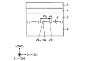
本発明の第1実施形態による窒化物系半導体発光素子の概略の断面を図1に示す。本実施形態の半導体発光素子は、表面に幅の異なる凸部2aおよび凹部2bを有する基板2上に形成されたn型のGaNからなるガイド層3と、このGaN層3上に形成されたInGaNからなる多重量子井戸構造の発光層4と、この発光層4上に形成されたp型のGaNからなるガイド層5とを備えている。なお、本実施形態においては、コンタクト層および電極は省略している。また、各層は<0001>方向(紙面上では上方向)に成長される。
次に、本発明の第2実施形態による窒化物系半導体発光ダイオード(LED)を図3に示す。
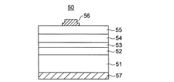
次に、本発明の第3実施形態による発光装置を図4に示す。本実施形態の発光装置は、より演色性の高い白色光を得るために第2実施形態の発光素子10をセラミック・パッケージ(外囲器)23内に配置されたサブマウント26上にフリップチップ実装し、赤色蛍光体材料を分散させた樹脂22で封止した構成となっている。本実施形態の発光装置においては、凹部を有するセラミック・パッケージ23の上記凹部の底部を貫通するように設けられたリード電極27上にサブマウント26が形成されている。このサブマウント26上に一対のバンプ25が設けられ、この一対のバンプ25に、第2実施形態の発光素子10の一対の電極18、19が接続されるように、発光素子10がフリップチップ実装されている。バンプ25の材料としては、金属バンプやはんだを使用するが、金バンプを用いると好ましい。バンプ25とリード電極27は金線等の導電性ワイヤなどでサブマウント26内部を貫通して接合し電気的導通を取る。リード電極27は電気伝導性が良いことが求められる。リード電極27の材料としては、鉄、銅、銅の合金等や、これらに銀、アルミニウム、金等の金属メッキが施されたものが使用できる。
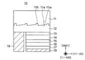
次に、本発明の第4実施形態による半導体発光素子を図5に示す。本実施形態の半導体発光素子30は、窒化物系半導体レーザ素子であって、第1実施形態と同様の凸部31aおよび凹部31bを有するn型GaNからなる基板31上に、n型GaN層32、n型AlGaNからなるクラッド層33、n型GaNからなる光ガイド層34、多重量子井戸構造のInGaNからなる活性層35、p型AlGaNからなるオーバーフロー防止層36、p型GaNからなる光ガイド層37、p型AlGaNからなるクラッド層38、p型GaN層39、およびp型GaNからなるコンタクト層40が、順次積層された積層構造を有している。なお、第1実施形態と同様に凸部31aの表面が<11−20>方向(紙面の右から左の方向)へ傾斜した傾斜面31a1となっている。また、凸部31aおよび凹部31bの幅は第1実施形態で説明した範囲に範囲の値となっている。本実施形態においては、凸部幅は400μm、凹部幅は30μmである。
次に、本発明の第5実施形態による半導体発光素子を説明する。
次に、本発明の第6実施形態による発光装置を図11乃至図15を参照して説明する。
次に、本発明の第7実施形態による半導体発光素子を説明する。
Nave=(n1・d1+・・・+nm・dm)/(d1+・・・+dm)
で表される値である。
3 n型GaNからなるガイド層
4 多重量子井戸構造のInGaNからなる発光層
5 p型GaNからなるガイド層
10 発光ダイオード
11 基板
12 n型GaNからなるコンタクト層
13 n型GaNからなるガイド層
14 多重量子井戸構造のInGaNからなる発光層
15 p型AlGaNからなるオーバーフロー防止層
16 p型GaNからなる層
17 p型GaNからなるコンタクト層
18 n側電極
19 p側電極
22 蛍光体を分散した封止樹脂
23 セラミック・パッケージ
25 バンプ
26 サブマウント
27 リード電極
30 半導体レーザ素子
31 基板
32 n型GaNからなるコンタクト層
33 n型AlGaNからなるクラッド層
34 n型GaNからなる光ガイド層
35 多重量子井戸構造のInGaNからなる活性層
36 p型AlGaNからなるオーバーフロー防止層
37 p型GaNからなるガイド層
38 p型AlGaNからなるクラッド層
39 p型GaNからなる層
40 p型GaNからなるコンタクト層
41 n側電極
42 p側電極
Claims (7)
- 複数の発光ダイオードであって、各発光ダイオードは、n型III族窒化物半導体層と、p型III族窒化物半導体層と、前記n型III族窒化物半導体層と前記p型III族窒化物半導体層との間に設けられた発光層と、を有する積層膜を備えた、複数の発光ダイオードと、
前記複数の発光ダイオードのうち、隣接する2つの発光ダイオードのうちの一方の発光ダイオードの前記n型III族窒化物半導体層と、他方の発光ダイオードの前記p型III族窒化物半導体層とを接続することにより、前記隣接する2つの前記発光ダイオードを直列に接続する配線であって、III族元素がドーピングされた、ZnOおよびMgOのうちのいずれかを含む配線と、
を備えた発光装置。 - 前記配線と、前記積層膜との間に設けられた絶縁層を更に備えた請求項1記載の発光装置。
- 前記n型III族窒化物半導体層および前記配線に接続するボンディングパッドを更に備え、前記ボンディングパッドは、前記n型III族窒化物半導体層に接続するZnO層と、前記ZnO層上に設けられたTi層、前記Ti層上に設けられたPt層、および前記Pt層上に設けられたAu層を有する積層膜とを備えた請求項1または2記載の発光装置。
- 前記配線に添加されるIII族元素はGaである請求項1乃至3のいずれかに記載の発光装置。
- 前記配線中のGaの濃度は、前記配線と前記n型III族窒化物半導体層との界面から離れるにつれて低くなり、かつ前記配線と前記p型III族窒化物半導体層との界面から離れるにつれて低くなる請求項4記載の発光装置。
- 前記複数の発光ダイオードは、半導体基板上に設けられ、前記半導体基板の表面には凹凸が設けられている請求項1乃至5のいずれかに記載の発光装置。
- 前記配線は、III族元素がドーピングされたZnOを含む請求項1乃至6のいずれかに記載の発光装置。
Priority Applications (1)
| Application Number | Priority Date | Filing Date | Title |
|---|---|---|---|
| JP2014132921A JP2014170977A (ja) | 2014-06-27 | 2014-06-27 | 発光装置 |
Applications Claiming Priority (1)
| Application Number | Priority Date | Filing Date | Title |
|---|---|---|---|
| JP2014132921A JP2014170977A (ja) | 2014-06-27 | 2014-06-27 | 発光装置 |
Related Parent Applications (1)
| Application Number | Title | Priority Date | Filing Date |
|---|---|---|---|
| JP2013167835A Division JP2013229638A (ja) | 2013-08-12 | 2013-08-12 | 半導体発光素子および発光装置 |
Publications (1)
| Publication Number | Publication Date |
|---|---|
| JP2014170977A true JP2014170977A (ja) | 2014-09-18 |
Family
ID=51693086
Family Applications (1)
| Application Number | Title | Priority Date | Filing Date |
|---|---|---|---|
| JP2014132921A Abandoned JP2014170977A (ja) | 2014-06-27 | 2014-06-27 | 発光装置 |
Country Status (1)
| Country | Link |
|---|---|
| JP (1) | JP2014170977A (ja) |
Cited By (1)
| Publication number | Priority date | Publication date | Assignee | Title |
|---|---|---|---|---|
| US9722162B2 (en) | 2015-09-10 | 2017-08-01 | Kabushiki Kaisha Toshiba | Semiconductor light emitting device |
Citations (6)
| Publication number | Priority date | Publication date | Assignee | Title |
|---|---|---|---|---|
| JP2000101136A (ja) * | 1998-09-25 | 2000-04-07 | Toshiba Corp | 半導体発光装置及び半導体発光装置の駆動方法 |
| JP2002289579A (ja) * | 2001-03-23 | 2002-10-04 | Mitsubishi Cable Ind Ltd | 結晶成長用基板、その製造方法、およびGaN系結晶の製造方法 |
| JP2005531154A (ja) * | 2002-06-26 | 2005-10-13 | アンモノ・スプウカ・ジ・オグラニチョノン・オドポヴィエドニアウノシツィオン | 窒化物半導体レーザ素子及びその性能を向上させる方法 |
| JP2006073815A (ja) * | 2004-09-02 | 2006-03-16 | Rohm Co Ltd | 半導体発光装置 |
| WO2006090571A1 (ja) * | 2005-02-22 | 2006-08-31 | Konica Minolta Opto, Inc. | 発光ダイオードとその製造方法 |
| JP2007019488A (ja) * | 2005-06-09 | 2007-01-25 | Rohm Co Ltd | 半導体発光素子 |
-
2014
- 2014-06-27 JP JP2014132921A patent/JP2014170977A/ja not_active Abandoned
Patent Citations (6)
| Publication number | Priority date | Publication date | Assignee | Title |
|---|---|---|---|---|
| JP2000101136A (ja) * | 1998-09-25 | 2000-04-07 | Toshiba Corp | 半導体発光装置及び半導体発光装置の駆動方法 |
| JP2002289579A (ja) * | 2001-03-23 | 2002-10-04 | Mitsubishi Cable Ind Ltd | 結晶成長用基板、その製造方法、およびGaN系結晶の製造方法 |
| JP2005531154A (ja) * | 2002-06-26 | 2005-10-13 | アンモノ・スプウカ・ジ・オグラニチョノン・オドポヴィエドニアウノシツィオン | 窒化物半導体レーザ素子及びその性能を向上させる方法 |
| JP2006073815A (ja) * | 2004-09-02 | 2006-03-16 | Rohm Co Ltd | 半導体発光装置 |
| WO2006090571A1 (ja) * | 2005-02-22 | 2006-08-31 | Konica Minolta Opto, Inc. | 発光ダイオードとその製造方法 |
| JP2007019488A (ja) * | 2005-06-09 | 2007-01-25 | Rohm Co Ltd | 半導体発光素子 |
Cited By (2)
| Publication number | Priority date | Publication date | Assignee | Title |
|---|---|---|---|---|
| US9722162B2 (en) | 2015-09-10 | 2017-08-01 | Kabushiki Kaisha Toshiba | Semiconductor light emitting device |
| US10134806B2 (en) | 2015-09-10 | 2018-11-20 | Alpad Corporation | Semiconductor light emitting device |
Similar Documents
| Publication | Publication Date | Title |
|---|---|---|
| JP5032171B2 (ja) | 半導体発光素子およびその製造方法ならびに発光装置 | |
| KR101384056B1 (ko) | 반도체 발광 소자 | |
| US9048385B2 (en) | Nitride semiconductor light emitting diode | |
| US6876009B2 (en) | Nitride semiconductor device and a process of manufacturing the same | |
| US9172019B2 (en) | Light emitting device package and method of manufacturing the same | |
| JP5788046B2 (ja) | 半導体発光素子 | |
| KR101646664B1 (ko) | 발광 소자, 발광 소자의 제조방법 및 발광 소자 패키지 | |
| JP2012195321A (ja) | 半導体発光素子 | |
| JP2014197704A (ja) | 発光デバイスおよび発光デバイスの作製方法 | |
| KR20110128545A (ko) | 발광 소자, 발광 소자의 제조방법 및 발광 소자 패키지 | |
| JP2009130097A (ja) | Iii族窒化物半導体発光素子及びその製造方法 | |
| KR20130058406A (ko) | 반도체 발광소자 | |
| JP5740350B2 (ja) | 半導体発光素子 | |
| JP4325160B2 (ja) | 窒化物半導体発光素子 | |
| JP2013229638A (ja) | 半導体発光素子および発光装置 | |
| JP5075298B1 (ja) | 窒化物系半導体発光素子およびその製造方法 | |
| JP5543946B2 (ja) | 半導体発光素子および発光装置 | |
| JP2009123836A (ja) | 窒化物半導体発光素子 | |
| JP2014170977A (ja) | 発光装置 | |
| JP2013033921A (ja) | 窒化物系発光ダイオード素子およびその製造方法 | |
| JP6010169B2 (ja) | 半導体発光素子 | |
| JP2017017144A (ja) | 窒化物半導体発光素子 | |
| JP2014099663A (ja) | 半導体発光素子 | |
| KR20130068701A (ko) | 발광소자 및 이를 포함하는 발광 소자 패키지 | |
| JP2012244148A (ja) | 半導体発光素子 |
Legal Events
| Date | Code | Title | Description |
|---|---|---|---|
| A621 | Written request for application examination |
Free format text: JAPANESE INTERMEDIATE CODE: A621 Effective date: 20140627 |
|
| A131 | Notification of reasons for refusal |
Free format text: JAPANESE INTERMEDIATE CODE: A131 Effective date: 20150616 |
|
| A521 | Written amendment |
Free format text: JAPANESE INTERMEDIATE CODE: A523 Effective date: 20150731 |
|
| A01 | Written decision to grant a patent or to grant a registration (utility model) |
Free format text: JAPANESE INTERMEDIATE CODE: A01 Effective date: 20151127 |
|
| A762 | Written abandonment of application |
Free format text: JAPANESE INTERMEDIATE CODE: A762 Effective date: 20151217 |