JP2014149335A - Substrate for electro-optic device, electro-optic device, and electronic equipment - Google Patents
Substrate for electro-optic device, electro-optic device, and electronic equipment Download PDFInfo
- Publication number
- JP2014149335A JP2014149335A JP2013016572A JP2013016572A JP2014149335A JP 2014149335 A JP2014149335 A JP 2014149335A JP 2013016572 A JP2013016572 A JP 2013016572A JP 2013016572 A JP2013016572 A JP 2013016572A JP 2014149335 A JP2014149335 A JP 2014149335A
- Authority
- JP
- Japan
- Prior art keywords
- substrate
- layer
- light
- light shielding
- shielding layer
- Prior art date
- Legal status (The legal status is an assumption and is not a legal conclusion. Google has not performed a legal analysis and makes no representation as to the accuracy of the status listed.)
- Pending
Links
Images


Abstract
Description
本発明は、電気光学装置用基板、電気光学装置、および電子機器に関する。 The present invention relates to a substrate for an electro-optical device, an electro-optical device, and an electronic apparatus.
表示領域に複数の画素およびスイッチング素子が設けられた素子基板と、素子基板に対向配置された対向基板と、の間に電気光学物質(例えば、液晶など)を備えた電気光学装置が知られている。電気光学装置として、例えば、プロジェクターの液晶ライトバルブとして用いられる液晶装置などを挙げることができる。このような液晶装置においては、明るさやコントラストを向上することが求められている。 There is known an electro-optical device including an electro-optical material (for example, liquid crystal) between an element substrate in which a plurality of pixels and switching elements are provided in a display area, and a counter substrate disposed to face the element substrate. Yes. Examples of the electro-optical device include a liquid crystal device used as a liquid crystal light valve of a projector. Such a liquid crystal device is required to improve brightness and contrast.
液晶装置において、スイッチング素子としてのTFTに光が入射して光リーク電流が生じることによる誤動作や表示品質の低下を防止するため、素子基板に遮光層を設けるとともに、対向基板にも遮光層を設ける構成が知られている(例えば、特許文献1参照)。対向基板にも遮光層を設けることで、隣り合う画素同士の間での光漏れが抑えられので、液晶装置のコントラストの向上を図ることができる。 In a liquid crystal device, a light shielding layer is provided on an element substrate and a light shielding layer is also provided on a counter substrate in order to prevent malfunction and deterioration of display quality due to light entering a TFT as a switching element and generating a light leakage current. The configuration is known (see, for example, Patent Document 1). By providing the light-blocking layer also on the counter substrate, light leakage between adjacent pixels can be suppressed, so that the contrast of the liquid crystal device can be improved.
ところで、対向基板のほぼ全面に共通電極(対向電極)が設けられるが、共通電極の厚さが厚いと光の透過率が低下するため、投射される画像の明るさが低下する。また、赤色光(R)、緑色光(G)、青色光(B)の色光毎に液晶装置を透過させて合成された光を投射する場合に、色光によって光の透過率のばらつきが大きいと、白く表示される画素が暗くなることや色相にずれが生じることがある。特許文献1に記載の液晶装置では、共通電極の厚さは約50nm〜200nmとされているが、共通電極の厚さがこのような範囲であると、表示の明るさや表示品質が低下するおそれがあるという課題がある。
By the way, a common electrode (counter electrode) is provided on almost the entire surface of the counter substrate. However, if the thickness of the common electrode is large, the light transmittance decreases, so that the brightness of the projected image decreases. Further, when projecting light synthesized by passing through a liquid crystal device for each color light of red light (R), green light (G), and blue light (B), if the light transmittance varies greatly by the color light, The pixels displayed in white may become dark or the hue may be shifted. In the liquid crystal device described in
また、液晶装置の表示の明るさを向上させるために共通電極の厚さを薄くすると、共通電極の抵抗値の増大を招くこととなる。共通電極の抵抗値が増大すると、共通電極における電位にぶれが生じて、液晶装置の表示にフリッカーが発生するなど表示品質の低下を招くという課題がある。さらに、共通電極の厚さを薄くすると、共通電極の下層の段差が大きい場合に、共通電極に不連続部分やクラックなどが発生し易くなるという課題がある。したがって、共通電極の抵抗値を増大させることや共通電極にクラックなどを発生させることなく、共通電極の厚さを薄くして、表示の明るさと表示品質とを向上できる液晶装置が求められている。 Further, if the thickness of the common electrode is reduced in order to improve the display brightness of the liquid crystal device, the resistance value of the common electrode is increased. When the resistance value of the common electrode increases, there is a problem in that the display quality is deteriorated, for example, the potential at the common electrode is fluctuated and flicker occurs in the display of the liquid crystal device. Furthermore, when the thickness of the common electrode is reduced, there is a problem that a discontinuous portion, a crack, or the like is likely to occur in the common electrode when the level difference in the lower layer of the common electrode is large. Accordingly, there is a need for a liquid crystal device capable of reducing the thickness of the common electrode and improving the display brightness and display quality without increasing the resistance value of the common electrode or causing cracks in the common electrode. .
本発明は、上述の課題の少なくとも一部を解決するためになされたものであり、以下の形態または適用例として実現することが可能である。 SUMMARY An advantage of some aspects of the invention is to solve at least a part of the problems described above, and the invention can be implemented as the following forms or application examples.
[適用例1]本適用例に係る電気光学装置用基板は、第1部材と、前記第1部材上に配置された第2部材と、前記第2部材の表面側に設けられ、複数の画素の各々に対応する複数の開口部を有する遮光層と、前記第2部材と前記遮光層とを覆うとともに、前記遮光層に接するように設けられた共通電極と、を備え、前記遮光層は金属材料で構成されており、前記共通電極の厚さは22nm以下であり、前記第2部材の表面と前記遮光層の表面との間隔は、前記共通電極の厚さ以下であることを特徴とする。 Application Example 1 An electro-optical device substrate according to this application example is provided with a first member, a second member disposed on the first member, and a surface side of the second member, and includes a plurality of pixels. A light-shielding layer having a plurality of openings corresponding to each of the light-shielding layer, a common electrode provided to cover the second member and the light-shielding layer and to be in contact with the light-shielding layer. The common electrode has a thickness of 22 nm or less, and a distance between the surface of the second member and the surface of the light shielding layer is equal to or less than the thickness of the common electrode. .
本適用例の構成によれば、遮光層が金属材料で構成され、共通電極が遮光層に接するように設けられているので、共通電極は遮光層と電気的に接続される。したがって、共通電極の厚さを薄くしても、遮光層に接していることで共通電極の抵抗値の増大が抑えられる。ここで、発明者らの測定結果によれば、共通電極の厚さを22nm以下とすれば、良好な明るさが得られることが分かっている。そして、共通電極の下層である第2部材の表面と遮光層の表面との間隔(段差)が共通電極の厚さ以下であるので、共通電極の厚さを薄くしても、第2部材の表面と遮光層の表面との段差に起因するクラックなどの発生が抑えられる。これらにより、共通電極の抵抗値を増大させることや共通電極にクラックなどを発生させることなく、共通電極の厚さを薄くすることができる。この結果、電気光学装置用基板を液晶装置に用いた場合に、明るく表示品質の高い液晶装置を提供することができる。 According to the configuration of this application example, the light shielding layer is made of a metal material, and the common electrode is provided so as to be in contact with the light shielding layer. Therefore, the common electrode is electrically connected to the light shielding layer. Therefore, even if the thickness of the common electrode is reduced, an increase in the resistance value of the common electrode can be suppressed by being in contact with the light shielding layer. Here, according to the measurement results of the inventors, it is known that good brightness can be obtained if the thickness of the common electrode is 22 nm or less. And since the space | interval (step) of the surface of the 2nd member which is a lower layer of a common electrode and the surface of a light shielding layer is below the thickness of a common electrode, even if the thickness of a common electrode is made thin, Occurrence of cracks and the like due to a step between the surface and the surface of the light shielding layer is suppressed. Accordingly, it is possible to reduce the thickness of the common electrode without increasing the resistance value of the common electrode or generating cracks in the common electrode. As a result, when the electro-optical device substrate is used in a liquid crystal device, a bright liquid crystal device with high display quality can be provided.
[適用例2]上記適用例に係る電気光学装置用基板であって、前記第2部材の前記表面には、前記複数の開口部のうちの隣り合う開口部の間に溝が設けられており、前記遮光層は、前記溝の内部に設けられていることが好ましい。 Application Example 2 In the electro-optical device substrate according to the application example described above, a groove is provided between adjacent openings of the plurality of openings on the surface of the second member. The light shielding layer is preferably provided inside the groove.
本適用例の構成によれば、第2部材の表面に溝が設けられ、その溝の内部に遮光層が設けられているので、遮光層の厚さを薄くしなくても、第2部材の表面と遮光層の表面との間隔を小さくできる。換言すれば、第2部材の表面に遮光層が設けられている場合と比べて、遮光層の厚さをより厚くして共通電極の抵抗値を低下させることが可能となる。したがって、共通電極の厚さを薄く形成しても、遮光層により共通電極の抵抗値の増大をより確実に抑えることができる。また、遮光層の厚さをより厚くすることで遮光性も向上する。 According to the configuration of this application example, since the groove is provided on the surface of the second member and the light shielding layer is provided inside the groove, the second member can be formed without reducing the thickness of the light shielding layer. The distance between the surface and the surface of the light shielding layer can be reduced. In other words, the resistance value of the common electrode can be reduced by increasing the thickness of the light shielding layer as compared with the case where the light shielding layer is provided on the surface of the second member. Therefore, even if the common electrode is formed thin, an increase in the resistance value of the common electrode can be more reliably suppressed by the light shielding layer. Further, the light shielding property is improved by increasing the thickness of the light shielding layer.
[適用例3]上記適用例に係る電気光学装置用基板であって、前記第1部材には、前記複数の開口部の各々に対応してマイクロレンズが設けられていることが好ましい。 Application Example 3 In the electro-optical device substrate according to the application example, it is preferable that the first member is provided with a microlens corresponding to each of the plurality of openings.
本適用例の構成によれば、複数の開口部の各々に対応して第1部材にマイクロレンズが設けられている。そのため、第1部材側から入射しそのまま直進すると遮光層で遮光されてしまう光のうちの一部を、マイクロレンズにより各開口部内に集光することができるので、光の利用効率を向上させることができる。また、第2部材の溝の内部に遮光層が設けられていると、第2部材の表面に遮光層が設けられている場合と比べて、遮光層を第1部材側に近づけることができるので、遮光層の開口率を高めることが可能となる。そして、遮光層を第1部材側に近づけることで、斜め方向からの光が隣の開口部に入射することを低減できる。これにより、電気光学装置用基板を液晶装置に用いた場合に、より明るく表示品質の高い液晶装置を提供することができる。 According to the configuration of this application example, the microlens is provided on the first member corresponding to each of the plurality of openings. Therefore, a part of the light that is incident from the first member side and goes straight as it is and is shielded by the light shielding layer can be condensed into each opening by the microlens, thereby improving the light utilization efficiency. Can do. Further, when the light shielding layer is provided inside the groove of the second member, the light shielding layer can be brought closer to the first member side as compared with the case where the light shielding layer is provided on the surface of the second member. Thus, the aperture ratio of the light shielding layer can be increased. And it can reduce that the light from an oblique direction injects into the adjacent opening part by making a light shielding layer close to the 1st member side. Accordingly, when the electro-optical device substrate is used in a liquid crystal device, a brighter and higher display quality liquid crystal device can be provided.
[適用例4]上記適用例に係る電気光学装置用基板であって、前記第1部材には、前記複数の開口部のうちの隣り合う開口部の間に反射部が設けられていることが好ましい。 Application Example 4 In the electro-optical device substrate according to the application example described above, the first member is provided with a reflection portion between adjacent openings of the plurality of openings. preferable.
本適用例の構成によれば、第1部材における開口部同士の間に反射部が設けられている。そのため、各開口部から外れて遮光層で遮光されてしまう光のうちの一部を、反射部で反射させて各開口部内に向かわせることができるので、光の利用効率を向上させることができる。また、第2部材の溝の内部に遮光層が設けられていると、第2部材の表面に遮光層が設けられている場合と比べて、遮光層を第1部材側に近づけることができるので、遮光層の開口率を高めることが可能となる。 According to the configuration of this application example, the reflection portion is provided between the openings in the first member. Therefore, a part of the light that is removed from each opening and is blocked by the light blocking layer can be reflected by the reflecting portion and directed into each opening, so that the light use efficiency can be improved. . Further, when the light shielding layer is provided inside the groove of the second member, the light shielding layer can be brought closer to the first member side as compared with the case where the light shielding layer is provided on the surface of the second member. Thus, the aperture ratio of the light shielding layer can be increased.
[適用例5]上記適用例に係る電気光学装置用基板であって、前記第1部材には、前記複数の開口部の各々に対応してカラーフィルターが設けられていることが好ましい。 Application Example 5 In the electro-optical device substrate according to the application example, it is preferable that the first member is provided with a color filter corresponding to each of the plurality of openings.
本適用例の構成によれば、第1部材に複数の開口部の各々に対応してカラーフィルターが設けられている。そのため、各開口部において特定の波長域の色光を透過させることができるので、電気光学装置用基板を液晶装置に用いた場合に、フルカラー表示が可能でより明るく表示品質の高い液晶装置を提供することができる。 According to the configuration of this application example, the first member is provided with the color filter corresponding to each of the plurality of openings. Therefore, since color light in a specific wavelength range can be transmitted through each opening, a full-color display capable of full color display and a brighter display quality can be provided when an electro-optical device substrate is used in the liquid crystal device. be able to.
[適用例6]本適用例に係る電気光学装置は、複数の画素電極と、前記複数の画素電極の各々に対応するスイッチング素子と、が設けられた第1基板と、前記第1基板に対向配置された第2基板と、前記第1基板と前記第2基板との間に配置された電気光学物質層と、を備え、前記第2基板が、上記適用例の電気光学装置用基板であることを特徴とする。 Application Example 6 An electro-optical device according to this application example is provided with a first substrate provided with a plurality of pixel electrodes and switching elements corresponding to the pixel electrodes, and opposed to the first substrate. A second substrate disposed; and an electro-optic material layer disposed between the first substrate and the second substrate, wherein the second substrate is a substrate for an electro-optic device according to the application example. It is characterized by that.
本適用例の構成によれば、電気光学物質層を挟持する一対の基板のうちの一方の基板に上記の電気光学装置用基板を備えることで、表示の明るさと表示品質とに優れた電気光学装置を提供することができる。 According to the configuration of this application example, the above-described electro-optic device substrate is provided on one of the pair of substrates sandwiching the electro-optic material layer, so that the electro-optic having excellent display brightness and display quality is achieved. An apparatus can be provided.
[適用例7]本適用例に係る電子機器は、上記適用例の電気光学装置を備えていることを特徴とする。 Application Example 7 An electronic apparatus according to this application example includes the electro-optical device according to the application example described above.
本適用例の構成によれば、表示の明るさと表示品質とに優れた電気光学装置を備えた電子機器を提供することができる。 According to the configuration of this application example, it is possible to provide an electronic apparatus including an electro-optical device that is excellent in display brightness and display quality.
以下、本発明を具体化した実施形態について図面を参照して説明する。使用する図面は、説明する部分が認識可能な状態となるように、適宜拡大、縮小、あるいは誇張して表示している。また、説明に必要な構成要素以外は図示を省略する場合がある。 DESCRIPTION OF EXEMPLARY EMBODIMENTS Hereinafter, embodiments of the invention will be described with reference to the drawings. The drawings to be used are appropriately enlarged, reduced or exaggerated so that the part to be described can be recognized. In addition, illustrations of components other than those necessary for the description may be omitted.
なお、以下の形態において、例えば「基板上に」と記載された場合、基板の上に接するように配置される場合、または基板の上に他の構成物を介して配置される場合、または基板の上に一部が接するように配置され、一部が他の構成物を介して配置される場合を表すものとする。 In the following embodiments, for example, when “on the substrate” is described, the substrate is disposed so as to be in contact with the substrate, or is disposed on the substrate via another component, or the substrate. It is assumed that a part is arranged so as to be in contact with each other and a part is arranged via another component.
(第1の実施形態)
<電気光学装置>
ここでは、電気光学装置として、薄膜トランジスター(Thin Film Transistor:TFT)を画素のスイッチング素子として備えたアクティブマトリックス型の液晶装置を例に挙げて説明する。この液晶装置は、例えば、後述する投射型表示装置(プロジェクター)の光変調素子(液晶ライトバルブ)として好適に用いることができるものである。
(First embodiment)
<Electro-optical device>
Here, an active matrix liquid crystal device including a thin film transistor (TFT) as a pixel switching element will be described as an example of the electro-optical device. This liquid crystal device can be suitably used, for example, as a light modulation element (liquid crystal light valve) of a projection display device (projector) described later.
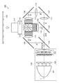
まず、第1の実施形態に係る電気光学装置としての液晶装置について、図1、図2、および図3を参照して説明する。図1は、第1の実施形態に係る液晶装置の構成を示す概略図である。詳しくは、図1(a)は液晶装置の構成を示す概略平面図であり、図1(b)は図1(a)のH−H’線に沿った概略断面図である。図2は、第1の実施形態に係る液晶装置の電気的な構成を示す等価回路図である。また、図3は、第1の実施形態に係る液晶装置の構造を示す概略断面図である。詳しくは、図3は、図1のA−A’線に沿った概略断面図である。 First, a liquid crystal device as an electro-optical device according to the first embodiment will be described with reference to FIGS. 1, 2, and 3. FIG. 1 is a schematic diagram illustrating the configuration of the liquid crystal device according to the first embodiment. Specifically, FIG. 1A is a schematic plan view showing the configuration of the liquid crystal device, and FIG. 1B is a schematic cross-sectional view taken along the line H-H ′ of FIG. FIG. 2 is an equivalent circuit diagram showing an electrical configuration of the liquid crystal device according to the first embodiment. FIG. 3 is a schematic cross-sectional view showing the structure of the liquid crystal device according to the first embodiment. Specifically, FIG. 3 is a schematic cross-sectional view taken along the line A-A ′ of FIG. 1.
図1(a)および(b)に示すように、第1の実施形態に係る液晶装置1は、第1基板としての素子基板20と、素子基板20に対向配置された第2基板としての対向基板30と、素子基板20と対向基板30との間に配置された電気光学物質層としての液晶層40とを備えている。本実施形態では、対向基板30が本発明の電気光学装置用基板に該当する。
As shown in FIGS. 1A and 1B, the
液晶装置1は、例えば、TN(Twisted Nematic)モードやVA(Vertical Alignment)モードで動作する。液晶装置1は、対向基板30側から入射した光を変調して素子基板20側に射出する透過型の液晶装置である。
The
図1(a)および(b)に示すように、素子基板20は対向基板30よりも一回り大きく、両基板は、額縁状に配置されたシール材42を介して接合されている。液晶層40は、素子基板20と対向基板30とシール材42とによって囲まれた空間に封入された、電気光学物質としての正または負の誘電異方性を有する液晶で構成されている。
As shown in FIGS. 1A and 1B, the
シール材42は、例えば熱硬化性または紫外線硬化性のエポキシ樹脂などの接着剤からなる。シール材42には、素子基板20と対向基板30との間隔を一定に保持するためのスペーサー(図示省略)が混入されている。額縁状に配置されたシール材42の内側には、対向基板30に設けられた額縁状の遮光層32が配置されている。遮光層32は、遮光性を有する金属あるいは金属酸化物などの金属材料からなる。
The sealing
遮光層32の内側は、複数の画素Pが配列された表示領域Eとなっている。表示領域Eは、液晶装置1において、実質的に表示に寄与する領域である。なお、図1(a)および(b)では図示を省略したが、遮光層32は、表示領域Eの内側にも、複数の画素Pを平面的に区画するように格子状に設けられている。
Inside the
素子基板20の1辺部のシール材42の外側には、1辺部に沿ってデータ線駆動回路51および複数の外部接続端子54が設けられている。また、その1辺部に対向する他の1辺部に沿ったシール材42の内側には、検査回路53が設けられている。さらに、これらの2辺部と直交し互いに対向する他の2辺部に沿ったシール材42の内側には、走査線駆動回路52が設けられている。
A data
検査回路53が設けられた1辺部のシール材42の内側には、2つの走査線駆動回路52を繋ぐ複数の配線55が設けられている。これらデータ線駆動回路51、走査線駆動回路52に繋がる配線は、複数の外部接続端子54に接続されている。また、対向基板30の角部には、素子基板20と対向基板30との間で電気的導通をとるための上下導通部56が設けられている。なお、検査回路53の配置はこれに限定されず、データ線駆動回路51と表示領域Eとの間のシール材42の内側に沿った位置に設けてもよい。
A plurality of
以下の説明では、データ線駆動回路51が設けられた1辺部に沿った方向をX方向とし、この1辺部と直交し互いに対向する他の2辺部に沿った方向をY方向とする。図1(a)のH−H’線の方向は、Y方向に沿った方向である。また、X方向およびY方向と直交し図1(b)における上方に向かう方向をZ方向とする。なお、本明細書では、液晶装置1の対向基板30の表面の法線方向(Z方向)から見ることを「平面視」という。
In the following description, the direction along one side where the data line driving
図1(b)に示すように、素子基板20の液晶層40側には、画素P毎に設けられたスイッチング素子としてのTFT24(図3参照)と、光透過性を有する画素電極28と、信号配線(図示しない)と、画素電極28を覆う配向膜29とが設けられている。画素電極28は、ITO(Indium Tin Oxide)やIZO(Indium Zinc Oxide)などの光透過性を有する導電膜からなる。
As shown in FIG. 1B, on the
対向基板30は、後述するマイクロレンズ14(図3参照)が設けられた第1部材としてのマイクロレンズアレイ基板10を備えている。対向基板30の液晶層40側、すなわちマイクロレンズアレイ基板10上には、第2部材としての光路長調整層31と、遮光層32と、共通電極(対向電極)34と、共通電極34を覆う配向膜35とが設けられている。
The
遮光層32は、図1(a)および(b)に示すように、平面的に走査線駆動回路52、複数の配線55や検査回路53と重なる領域に額縁状に設けられている。遮光層32は、対向基板30側から入射する光を遮蔽して、これらの駆動回路を含む周辺回路の光による誤動作を防止する役目を果たしている。また、不必要な迷光が表示領域Eに入射しないように遮蔽して、表示領域Eの表示における高いコントラストを確保している。
As shown in FIGS. 1A and 1B, the
共通電極34は、例えばITO(Indium Tin Oxide)やIZO(Indium Zinc Oxide)などの光透過性を有する導電膜からなる。共通電極34は、図1(a)に示すように対向基板30の四隅に設けられた上下導通部56により素子基板20側の配線に電気的に接続されている。また、共通電極34は、光路長調整層31と遮光層32とを覆うとともに、遮光層32に接するように設けられている。
The
配向膜29および配向膜35は、液晶装置1の光学設計に基づいて選定される。配向膜29および配向膜35は、例えば、ポリイミドなどの有機材料を成膜して、その表面をラビングすることにより、液晶分子を略水平に配向させる処理が施されたものや、SiOx(酸化シリコン)などの無機材料を気相成長法を用いて成膜して、液晶分子を略垂直に配向させる処理が施されたものが挙げられる。
The
液晶層40を構成する液晶は、印加される電圧レベルにより分子集合の配向や秩序が変化することにより、光を変調し、階調表示を可能とする。例えば、ノーマリーホワイトモードの場合、各画素Pの単位で印加された電圧に応じて入射光に対する透過率が減少する。ノーマリーブラックモードの場合、各画素Pの単位で印加された電圧に応じて入射光に対する透過率が増加し、全体として液晶装置1からは画像信号に応じたコントラストをもつ光が射出される。
The liquid crystal constituting the
図2に示すように、表示領域Eには、走査線2とデータ線3とが互いに絶縁され交差するように形成されている。走査線2が延在する方向がX方向であり、データ線3が延在する方向がY方向である。画素Pは、走査線2とデータ線3との交差に対応して設けられている。画素Pのそれぞれには、画素電極28と、スイッチング素子としてのTFT24(Thin Film Transistor:薄膜トランジスター)とが設けられている。
As shown in FIG. 2, in the display area E, the
TFT24のソース電極(図示しない)は、データ線駆動回路51から延在するデータ線3に電気的に接続されている。データ線3には、データ線駆動回路51(図1参照)から画像信号(データ信号)S1、S2、…、Snが線順次で供給される。TFT24のゲート電極(図示しない)は、走査線駆動回路52から延在する走査線2の一部である。走査線2には、走査線駆動回路52から走査信号G1、G2、…、Gmが線順次で供給される。TFT24のドレイン電極(図示しない)は、画素電極28に電気的に接続されている。
A source electrode (not shown) of the
画像信号S1、S2、…、Snは、TFT24を一定期間だけオン状態とすることにより、データ線3を介して画素電極28に所定のタイミングで書き込まれる。このようにして画素電極28を介して液晶層40に書き込まれた所定レベルの画像信号は、対向基板30に設けられた共通電極34(図3参照)との間に形成される液晶容量で一定期間保持される。
The image signals S1, S2,..., Sn are written to the
なお、保持された画像信号S1、S2、…、Snがリークするのを防止するため、データ線3に沿って平行するように形成された容量線4と画素電極28との間に蓄積容量5が形成され、液晶容量と並列に配置されている。このように、各画素Pの液晶に電圧信号が印加されると、印加された電圧レベルにより液晶の配向状態が変化する。これにより、液晶層40(図3参照)に入射した光が変調されて階調表示が可能となる。
In order to prevent leakage of the held
図3に示すように、素子基板20は、基板21と、遮光層22と、絶縁層23と、TFT24と、絶縁層25と、遮光層26と、絶縁層27と、画素電極28と、配向膜29とを備えている。基板21は、例えばガラスや石英などの光透過性を有する材料からなる。
As shown in FIG. 3, the
遮光層22は、上層の遮光層26に平面視で重なるように格子状に形成されている。遮光層22および遮光層26は、素子基板20の厚さ方向(Z方向)において、TFT24を間に挟むように配置されている。遮光層22および遮光層26は、遮光性を有する金属材料などからなる。遮光層22および遮光層26が設けられていることにより、TFT24への光の入射が抑制される。
The
遮光層22および遮光層26は、複数の画素Pのうちの隣り合う画素P同士の間に配置されている。遮光層22および遮光層26は、それぞれ各画素Pに対応する開口部22a、開口部26aを有している。開口部22aおよび開口部26aは、光が透過する領域となる。
The
絶縁層23は、基板21と遮光層22とを覆うように設けられている。絶縁層23は、例えば、SiO2などの無機材料からなる。TFT24は、絶縁層23上に設けられている。TFT24は、画素電極28を駆動するスイッチング素子である。図示を省略するが、TFT24は、半導体層、ゲート電極、ソース電極、およびドレイン電極などで構成されている。
The insulating
ゲート電極は、素子基板20において平面視で半導体層のチャネル領域と重なる領域に絶縁層25の一部(ゲート絶縁膜)を介して形成されている。図示を省略するが、ゲート電極は、下層側に配置された走査線2(図2参照)にコンタクトホールを介して電気的に接続されており、ゲート電極に走査信号が印加されることによってTFT24のオン/オフが制御される。
The gate electrode is formed on the
絶縁層25は、絶縁層23とTFT24とを覆うように設けられている。絶縁層25は、例えば、SiO2などの無機材料からなる。絶縁層25は、TFT24の半導体層とゲート電極との間を絶縁するゲート絶縁膜を含む。絶縁層25により、TFT24によって生じる表面の凹凸が緩和される。絶縁層25上には、遮光層26が設けられている。そして、絶縁層25と遮光層26とを覆うように、無機材料からなる絶縁層27が設けられている。
The insulating
画素電極28は、絶縁層27上に、各画素Pに対応して設けられている。画素電極28は、遮光層22の開口部22aおよび遮光層26の開口部26aに平面視で重なる領域に配置されている。配向膜29は、画素電極28を覆うように設けられている。
The
なお、TFT24、TFT24に電気信号を供給する電極や走査線2およびデータ線3などの配線(図示しない)は、平面視で遮光層22および遮光層26に重なる領域に設けられている。TFT24は、例えば、遮光層22および遮光層26の格子の交点、すなわち画素Pの4隅に設けられている。なお、これらの電極や配線などが遮光層22および遮光層26を兼ねる構成であってもよい。
Note that the
<電気光学装置用基板の構成>
第1の実施形態に係る電気光学装置用基板としての対向基板30は、第1部材としてのマイクロレンズアレイ基板10と、第2部材としての光路長調整層31と、遮光層32と、共通電極34と、配向膜35とを備えている。マイクロレンズアレイ基板10は、基板11とレンズ層13とを備えている。マイクロレンズアレイ基板10は、基板11に設けられた凹部12の開口部側が素子基板20に対向するように配置されている。
<Configuration of substrate for electro-optical device>
The
基板11は、例えばガラスや石英などの光透過性を有する材料からなる。基板11は、その液晶層40側の表面である面11aに形成された複数の凹部12を有している。凹部12は、各画素Pに対応して配置されている。凹部12は、その底部に向かって先細りとなる曲面状に形成されている。
The
レンズ層13は、基板11の面11a側に、凹部12を埋め込むように形成されている。レンズ層13は、光透過性を有し、基板11とは異なる光屈折率を有する材料からなる。より具体的には、レンズ層13は、基板11よりも光屈折率の高い材料からなる。レンズ層13の材料としては、例えばSiON、Al2O3などの無機材料や樹脂材料が挙げられる。
The
レンズ層13で凹部12を埋め込むことにより、凸状のマイクロレンズ14が構成される。各マイクロレンズ14は、各画素Pに対応して配置されている。これらの複数のマイクロレンズ14により、マイクロレンズアレイMLAが構成される。
By embedding the
光路長調整層31は、マイクロレンズアレイ基板10上に設けられている。光路長調整層31は、光透過性を有し、基板11とほぼ同じ光屈折率を有する。光路長調整層31は、例えば、シリコン酸化膜(SiO2)などの電気的絶縁性を有する無機材料からなる。光路長調整層31は、マイクロレンズ14の焦点距離を所望の値に合わせる機能を有する。したがって、光路長調整層31の層厚は、光の波長に応じたマイクロレンズ14の焦点距離などの光学条件に基づいて適宜設定される。
The optical path
光路長調整層31は、その液晶層40側の表面31aに形成された溝31bを有している。溝31bは、平面視で、表示領域E(図1(a)参照)の外側に設けられるとともに、表示領域Eの内側において遮光層22および遮光層26に重なる領域に格子状に設けられている。遮光層32は、溝31bの内部に設けられている。
The optical path
遮光層32は、平面視で、表示領域Eの外側に設けられるとともに、表示領域Eの内側において遮光層22および遮光層26に重なる領域に設けられており、複数の画素Pのうちの隣り合う画素P同士の間に配置されている。遮光層32は、各画素Pに対応する開口部32aを有している。開口部32a内は、光が透過する領域となる。遮光層32は、遮光性を有する金属あるいは金属酸化物などの金属材料からなり、例えば、チタンナイトライド(TiN)からなる。
The
共通電極34は、光路長調整層31と遮光層32とを覆うように設けられている。共通電極34は、複数の画素Pに跨って形成されている。共通電極34は、上述したように、ITO(Indium Tin Oxide)やIZO(Indium Zinc Oxide)などの光透過性を有する導電膜からなる。共通電極34は、遮光層32の表面32bに接している。したがって、共通電極34は、遮光層32に電気的に接続されている。共通電極34の厚さTは、22nm以下である。
The
配向膜35は、共通電極34を覆うように設けられている。液晶層40は、素子基板20側の配向膜29と対向基板30側の配向膜35との間に封入されている。
The
第1の実施形態に係る液晶装置1では、光は、対向基板30側(マイクロレンズアレイ基板10側)、すなわち、基板11の液晶層40とは反対側の表面である面11b側から入射し、マイクロレンズ14によって集光される。例えば、面11b側からマイクロレンズ14に入射する光のうち、画素Pの平面的な中心を通過する光軸に沿って入射した入射光L1は、マイクロレンズ14をそのまま直進し、液晶層40を通過して素子基板20側に射出される。
In the
入射光L1よりも外側の、平面視で遮光層32と重なる領域からマイクロレンズ14の周縁部に入射した入射光L2は、仮にそのまま直進した場合、破線で示すように遮光層32で遮光されてしまうが、基板11とレンズ層13との間の光屈折率の差により、画素P2の平面的な中心側へ屈折する。
The incident light L2 incident on the peripheral edge of the
液晶装置1では、このように直進した場合に遮光層32で遮光されてしまう入射光L2も、各マイクロレンズ14の集光作用により遮光層32の開口部32a内に入射させて液晶層40を通過させることができる。この結果、素子基板20側から射出される光の量を多くできるので、光の利用効率を高めることができる。
In the
また、液晶装置1では、光路長調整層31の溝31bの内部に遮光層32が設けられている。そのため、光路長調整層31の表面31aに遮光層32が設けられている場合と比べて、遮光層32をマイクロレンズアレイ基板10側により近付けることができるので、遮光層32の開口率を高めることが可能となる。そして、遮光層32をマイクロレンズアレイ基板10側に近付けることで、斜め方向からの光が隣の画素Pの領域に入射することを低減できる。
In the
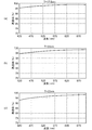
<共通電極の厚さと光透過率>
ここで、第1の実施形態に係る電気光学装置用基板としての対向基板30では、従来の液晶装置における電気光学装置用基板と比べて、共通電極34の厚さが薄くなっている。より具体的には、例えば特許文献1に記載の液晶装置では共通電極の厚さは約50nm〜200nmとされているが、本実施形態に係る液晶装置1では、共通電極34の厚さTを22nm以下としている。このように、共通電極34の厚さTを従来よりも薄くしている理由を、図4および図5を参照して説明する。
<Common electrode thickness and light transmittance>
Here, in the
図4および図5は、共通電極の厚さと光透過率との関係を示すグラフである。より具体的には、図4(a),(b),(c)および図5(a),(b),(c)の各図は、共通電極34の厚さTを、それぞれ、17.5nm、20nm、22nm、50nm、83.5nm、140nmに異ならせたときの、光の透過率の測定結果を示す図である。各図において、横軸は光の波長(nm)であり、縦軸は透過率(%)である。
4 and 5 are graphs showing the relationship between the thickness of the common electrode and the light transmittance. More specifically, in each of FIGS. 4A, 4B, and 5C and FIGS. 5A, 5B, and 5C, the thickness T of the
なお、後述するが、液晶装置1をプロジェクター100(図13参照)の液晶ライトバルブとして用いる場合、赤色光(R)、緑色光(G)、青色光(B)の各色光が液晶装置1を透過する。したがって、液晶装置1は、これら3つの色光のそれぞれを良好に透過させることが望ましい。赤色光(R)の波長域は600nm〜650nm程度であり、緑色光(G)の波長域は500nm〜550nm程度であり、青色光(B)の波長域は430nm〜480nm程度である。
As will be described later, when the
図4(a)に示すように、共通電極34の厚さTが17.5nmの場合、赤色光(R)、緑色光(G)、青色光(B)のそれぞれの波長域において、光の透過率は95%以上と良好である。図4(b)に示すように、共通電極34の厚さTが20nmの場合、厚さTが17.5nmの場合と比べて、青色光(B)の波長域でやや透過率が低下するものの、光の透過率は良好である。図4(c)に示すように、共通電極34の厚さTが22nmの場合、青色光(B)の波長域でさらに透過率が低下するものの、光の透過率は90%以上と良好である。
As shown in FIG. 4A, in the case where the thickness T of the
図5(a)に示すように、共通電極34の厚さTが50nmの場合、厚さTが22nm以下の場合と比べて、各波長域において光の透過率が低下し、赤色光(R)の波長域では光の透過率が90%以上となるものの、青色光(B)および緑色光(G)の波長域では光の透過率が90%未満となる。また、青色光(B)の波長域における光の透過率と赤色光(R)の波長域における光の透過率との差が大きくなってしまう。
As shown in FIG. 5A, when the thickness T of the
図5(b)に示すように、共通電極34の厚さTが83.5nmの場合は、各波長域において光の透過率が90%未満となってしまう。また、図5(c)に示すように、共通電極34の厚さTが140nmの場合、緑色光(G)の波長域では光の透過率が95%以上になるものの、赤色光(R)および青色光(B)およびの波長域では光の透過率が低下し、青色光(B)の波長域における光の透過率と緑色光(G)の波長域における光の透過率との差が大きくなってしまう。
As shown in FIG. 5B, when the thickness T of the
このように、光の透過率が低下すると、プロジェクター100から投射される画像が暗くなる。また、各色光の波長域における光の透過率のばらつきが大きいと、白く表示される画素Pにおいて、白色がくすんで見えたり、色相がずれて見えたりすることとなる。
Thus, when the light transmittance decreases, the image projected from the
図4および図5に示す測定結果によれば、共通電極34の厚さTが22nm以下では、光の透過率が良好であり各色光の波長域における光の透過率のばらつきが小さい。しかしながら、共通電極34の厚さTが50nm以上であると、少なくともいずれかの色光の波長域における光の透過率が低下し、色光によって光の透過率のばらつきが大きくなる。
According to the measurement results shown in FIGS. 4 and 5, when the thickness T of the
第1の実施形態に係る液晶装置1(対向基板30)では、上述の測定結果に基づいて、共通電極34の厚さTを22nm以下としている。したがって、液晶装置1では、特許文献1に記載の液晶装置と比べて、投射される画像を明るくでき、白く表示される画素Pにおいて白色がくすんで見えたり色相がずれて見えたりすることを抑えることができる。
In the liquid crystal device 1 (counter substrate 30) according to the first embodiment, the thickness T of the
一方、共通電極34の厚さTを薄くすると、共通電極34の抵抗値の増大を招いてしまう。そこで、第1の実施形態に係る液晶装置1では、図3に示すように、共通電極34を遮光層32に接するように設けることにより、共通電極34と遮光層32とを電気的に接続させている。遮光層32は、表示領域E(図1(a)参照)の外側に配置されるとともに、表示領域Eの内側にも隣り合う画素P同士の間に配置されており、平面視で共通電極34とほぼ重なる領域に設けられている。これにより、共通電極34の厚さTを薄くしても、共通電極34の抵抗値の増大を抑えることができる。
On the other hand, when the thickness T of the
また、共通電極34の厚さTを薄くすると、共通電極34の下層に位置する光路長調整層31の表面31aと遮光層32の表面32bとの間隔(段差)が大きい場合、共通電極34を成膜する際に不連続部分が生じることや、クラックなどが発生するおそれがある。そこで、第1の実施形態に係る液晶装置1では、光路長調整層31の表面31aと遮光層32の表面32bとの間隔を共通電極の厚さT以下としている。
In addition, when the thickness T of the
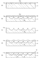
液晶装置1(対向基板30)における共通電極34の厚さと、光路長調整層31の表面31aと遮光層32の表面32bとの間隔について、図6を参照してさらに説明する。図6は、第1の実施形態に係る液晶装置の断面構造を拡大して示す図である。詳しくは、図6は、図1のA−A’線に沿った部分断面図であり、図3とは上下方向(Z方向)が反転している。
The thickness of the
図6(a),(b),(c)に示すように、第1の実施形態に係る液晶装置1では、上述した通り、遮光層32が、光路長調整層31の溝31bの内部に設けられている。そして、共通電極34が、光路長調整層31と遮光層32とを覆って設けられている。
As shown in FIGS. 6A, 6 </ b> B, and 6 </ b> C, in the
液晶装置1(対向基板30)において、図6(a)に示すように、光路長調整層31の表面31aと遮光層32の表面32bとがほぼ平坦な面となっていてもよい。光路長調整層31の表面31aと遮光層32の表面32bとがほぼ平坦な面であると、上層の共通電極34もほぼ平坦に形成される。
In the liquid crystal device 1 (counter substrate 30), as shown in FIG. 6A, the
液晶装置1(対向基板30)において、図6(b)に示すように、光路長調整層31の表面31aから遮光層32が突出しており、光路長調整層31の表面31aと遮光層32の表面32bとに段差が生じていてもよい。ただし、この場合、光路長調整層31の表面31aと遮光層32の表面32bとの間隔(段差)D1は、共通電極34の厚さT以下とする。
In the liquid crystal device 1 (counter substrate 30), as shown in FIG. 6B, the
図6(b)に示すように、光路長調整層31の表面31aから遮光層32が突出していることで、共通電極34の表面には遮光層32と重なる領域に凸条部が形成されることとなる。共通電極34がこのように形成されていても、光路長調整層31の表面31aと遮光層32の表面32bとの間隔D1を共通電極34の厚さT以下とすることで、共通電極34における不連続部分やクラックなどの発生を抑えることができる。
As shown in FIG. 6B, the
また、液晶装置1(対向基板30)において、図6(c)に示すように、光路長調整層31の表面31aから遮光層32が窪んで設けられ、光路長調整層31の表面31aと遮光層32の表面32bとに段差が生じていてもよい。ただし、この場合も、光路長調整層31の表面31aと遮光層32の表面32bとの間隔(段差)D2は、共通電極34の厚さT以下とする。
In the liquid crystal device 1 (counter substrate 30), as shown in FIG. 6C, the
図6(c)に示すように、光路長調整層31の表面31aから遮光層32が窪んでいることで、共通電極34の表面には遮光層32と重なる領域に凹条部が形成されることとなる。共通電極34がこのように形成されていても、光路長調整層31の表面31aと遮光層32の表面32bとの間隔D2を共通電極34の厚さT以下とすることで、共通電極34における不連続部分やクラックなどの発生を抑えることができる。
As shown in FIG. 6C, the
図6(a),(b),(c)において、遮光層32は光路長調整層31の溝31bの内部に設けられるので、遮光層32の厚さは限定されない。したがって、遮光層32の厚さをより厚くして共通電極34の抵抗値を低下させることが可能である。また、遮光層32の厚さをより厚くすることで遮光性も向上する。
6A, 6B, and 6C, since the
なお、本実施形態では、図6(a)に示すように、光路長調整層31の表面31aと遮光層32の表面32bとがほぼ平坦な面であることが好ましい。光路長調整層31の表面31aと遮光層32の表面32bとがほぼ平坦な面であると、共通電極34における不連続部分やクラックなどの発生をより確実に抑えることができる。
In the present embodiment, as shown in FIG. 6A, it is preferable that the
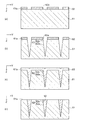
<電気光学装置用基板の製造方法>
次に、第1の実施形態に係る電気光学装置用基板としての対向基板30の製造方法を、図7および図8を参照して説明する。図7および図8は、第1の実施形態に係る電気光学装置用基板の製造方法を示す概略断面図である。なお、図7および図8の各図は、図1のA−A’線に沿った概略断面図に相当し、図3とは上下方向(Z方向)が反転している。
<Method for Manufacturing Electro-Optical Device Substrate>
Next, a manufacturing method of the
なお、図示しないが、対向基板30の製造工程では、対向基板30を複数枚取りできる大型の基板(マザー基板)で加工が行われ、最終的にそのマザー基板を切断して個片化することにより、複数の対向基板30が得られる。したがって、以下に説明する各工程では個片化する前のマザー基板の状態で加工が行われるが、ここでは、マザー基板の中の個別の対向基板30に対する加工について説明する。
Although not shown, in the manufacturing process of the
まず、図7(a)に示すように、石英などからなる光透過性を有する基板11の面11aに、例えば、多結晶シリコンなどでマスク層91を形成する。そして、例えば、フォトリソグラフィ技術を用いてパターニングし、マスク層91に開口部91aを形成する。開口部91aは、上述した画素Pの領域の平面的な中心位置に対応する位置に形成する。図7(a)は、マスク層91がパターニングされた後の状態を示している。
First, as shown in FIG. 7A, a
次に、図7(b)に示すように、マスク層91の開口部91aを介して基板11に、等方性エッチング処理を施すことにより、基板11に凹部12を形成する。等方性エッチング処理として、例えば、フッ酸溶液などのエッチング液を用いたウエットエッチングが用いられる。
Next, as shown in FIG. 7B, the
このエッチング処理により、基板11の面11a側から開口部91aを中心として等方的にエッチングされて、凹部12が形成される。凹部12は、平面視で、開口部91aを中心とする同心円状に形成される。続いて、図7(c)に示すように、基板11からマスク層91を除去する。
By this etching process, the
次に、図7(d)に示すように、基板11の面11a側にレンズ層13を形成する。レンズ層13は、光透過性を有し、基板11よりも光屈折率の高い無機材料を用いて、凹部12を埋め込むように形成する。レンズ層13は、例えばCVD(Chemical Vapor Deposition)法を用いて形成することができる。レンズ層13の上面には、凹部12と凹部12同士の間との段差が反映される。
Next, as illustrated in FIG. 7D, the
次に、レンズ層13に対して平坦化処理を施す。この工程では、例えば、CMP(Chemical Mechanical Polishing)処理などを用いて、レンズ層13の上面を研磨することにより、レンズ層13を平坦化する。なお、平坦化工程における平坦化処理の方法としては、CMP処理に限定されるものではなく、エッチバック法を用いてもよい。レンズ層13の層厚は、光路長調整層31の層厚と合わせて、光の波長に応じたマイクロレンズ14の焦点距離などの光学条件に基づいて適宜設定される。これにより、レンズ層13の上面が平坦化されて、マイクロレンズアレイ基板10が形成される。
Next, the
次に、図8(a)に示すように、マイクロレンズアレイ基板10のレンズ層13上に、光路長調整層31を形成する。光路長調整層31は、例えば、シリコン酸化膜を材料としてCVD法を用いて形成される。
Next, as shown in FIG. 8A, the optical path
次に、図8(b)に示すように、光路長調整層31に、表面31aから窪んだ溝31bを形成する。図示を省略するが、光路長調整層31の表面31aにマスク層を形成し、マスク層における遮光層32を形成する領域に開口部を形成する。そして、マスク層の開口部を介して光路長調整層31に、例えばドライエッチングなどの異方性エッチング処理を施すことにより、溝31bが形成される。
Next, as shown in FIG. 8B, a
次に、図8(c)に示すように、光路長調整層31の表面31aを覆い溝31bを埋めるように、遮光層32となる遮光膜を形成する。遮光膜(遮光層32)は、例えば、TiNを材料としてスパッタリング法を用いて堆積させることにより形成される。遮光膜(遮光層32)の上面には、表面31aと溝31bとの段差が反映される。
Next, as shown in FIG. 8C, a light shielding film to be the
次に、図8(d)に示すように、遮光膜(遮光層32)のうち、光路長調整層31の溝31bの内部にある部分以外の部分を除去する。この工程では、いわゆるダマシン法を用いることができる。ダマシン法では、CMP処理を用いて遮光膜(遮光層32)の上面を研磨することにより、遮光膜(遮光層32)のうちの光路長調整層31の表面31aを覆う部分が除去され、溝31bの内部に埋め込まれた部分が残る。これにより、図6(a)に示すように、光路長調整層31の表面31aと遮光層32の表面32bとの間隔を極力小さくしてほぼ平坦な面とすることができる。
Next, as shown in FIG. 8D, portions of the light shielding film (light shielding layer 32) other than the portion inside the
なお、図8(d)に示す工程において、遮光層32が研磨されるとともに光路長調整層31の表面31aも研磨されることで、遮光層32の残った部分が光路長調整層31の表面31aから突出した状態となってもよい。ただし、このような場合は、図6(b)に示すように、光路長調整層31の表面31aと遮光層32の表面32bとの間隔D1が共通電極34の厚さT以下であるものとする。
In the step shown in FIG. 8D, the
また、図8(d)に示す工程において、遮光層32が研磨されることで、遮光層32の残った部分が光路長調整層31の表面31aから窪んだ状態となってもよい。ただし、このような場合は、図6(c)に示すように、光路長調整層31の表面31aと遮光層32の表面32bとの間隔D2が共通電極34の厚さT以下であるものとする。
Further, in the step shown in FIG. 8D, the remaining portion of the
次に、図8(e)に示すように、光路長調整層31と遮光層32とを覆うように、共通電極34を形成する。共通電極34は、例えば、ITOを材料としてスパッタリング法を用いて、22nm以下の膜厚で堆積させることにより形成される。続いて、図示を省略するが、共通電極34上に配向膜35を形成する。以上で、対向基板30が完成する。
Next, as shown in FIG. 8E, the
以上説明したように、第1の実施形態によれば、以下に示す効果が得られる。 As described above, according to the first embodiment, the following effects can be obtained.
(1)遮光層32が金属材料で構成され、共通電極34が遮光層32に接するように設けられているので、共通電極34は遮光層32と電気的に接続されている。したがって、共通電極34の厚さTを、良好な明るさが得られる22nm以下に薄くしても、遮光層32に接していることで共通電極34の抵抗値の増大が抑えられる。そして、共通電極34の下層である光路長調整層31の表面31aと遮光層32の表面32bとの間隔(段差)D1,D2が共通電極34の厚さT以下であるので、共通電極34の厚さTを薄くしても、光路長調整層31の表面31aと遮光層32の表面32bとの間隔(段差)D1,D2に起因するクラックなどの発生が抑えられる。これらにより、共通電極34の抵抗値を増大させることや共通電極34にクラックなどを発生させることを抑止して、共通電極34の厚さTを薄くすることができる。この結果、明るく表示品質の高い液晶装置1を提供することができる。
(1) Since the
(2)光路長調整層31の表面31aに溝31bが設けられ、溝31bの内部に遮光層32が設けられているので、遮光層32の厚さを薄くしなくても、光路長調整層31の表面31aと遮光層32の表面32bとの間隔(段差)D1,D2を小さくできる。換言すれば、光路長調整層31の表面31aに遮光層32が設けられている場合と比べて、遮光層32の厚さをより厚くして共通電極34の抵抗値を低下させることが可能となる。したがって、共通電極34の厚さTを薄く形成しても、遮光層32により共通電極34の抵抗値の増大をより確実に抑えることができる。また、遮光層32の厚さをより厚くすることで遮光性も向上する。
(2) Since the
(3)各画素P(開口部32a)に対応してマイクロレンズアレイ基板10にマイクロレンズ14が設けられている。そのため、マイクロレンズアレイ基板10(基板11)側から入射しそのまま直進すると遮光層32で遮光されてしまう光のうちの一部を、マイクロレンズ14により各画素Pの領域(開口部32a)内に集光することができるので、光の利用効率を向上させることができる。また、光路長調整層31の溝31bの内部に遮光層32が設けられていると、光路長調整層31の表面31aに遮光層32が設けられている場合と比べて、遮光層32をマイクロレンズアレイ基板10側により近づけることができるので、遮光層32の開口率を高めることが可能となる。そして、遮光層32をマイクロレンズアレイ基板10側に近づけることで、斜め方向からの光が隣の画素Pの領域(開口部32a)に入射することを低減できる。これにより、より明るく表示品質の高い液晶装置1を提供することができる。
(3) The
(第2の実施形態)
<電気光学装置>
第2の実施形態に係る電気光学装置としての液晶装置は、第1の実施形態に係る液晶装置に対して、対向基板に反射部(プリズム)が設けられたプリズム基板を備えている点が異なるが、他の構成はほぼ同じである。なお、第1の実施形態と共通する構成要素については、同一の符号を付しその説明を省略する。
(Second Embodiment)
<Electro-optical device>
The liquid crystal device as the electro-optical device according to the second embodiment is different from the liquid crystal device according to the first embodiment in that the counter substrate includes a prism substrate provided with a reflective portion (prism). However, other configurations are almost the same. In addition, about the component which is common in 1st Embodiment, the same code | symbol is attached | subjected and the description is abbreviate | omitted.
第2の実施形態に係る液晶装置の構成について図9を参照して説明する。図9は、第2の実施形態に係る液晶装置の構成を示す概略断面図である。詳しくは、図9は、図1のA−A’線(X方向)に沿った概略断面図に相当する。 The configuration of the liquid crystal device according to the second embodiment will be described with reference to FIG. FIG. 9 is a schematic cross-sectional view showing the configuration of the liquid crystal device according to the second embodiment. Specifically, FIG. 9 corresponds to a schematic cross-sectional view along the line A-A ′ (X direction) in FIG. 1.
図9に示すように、第2の実施形態に係る液晶装置1Aは、第1基板としての素子基板20と、第2基板としての対向基板30Aと、液晶層40とを備えている。本実施形態では、対向基板30Aが本発明の電気光学装置用基板に該当する。
As shown in FIG. 9, the
<電気光学装置用基板の構成>
第2の実施形態に係る電気光学装置用基板としての対向基板30Aは、プリズム65が設けられた第1部材としてのプリズム基板60を備えている。対向基板30Aの液晶層40側、すなわちプリズム基板60上には、第2部材としての平坦化層33と、遮光層32と、共通電極34と、配向膜35とが設けられている。
<Configuration of substrate for electro-optical device>
The
プリズム基板60は、基板61と、基板61の液晶層40側の面61aに設けられたプリズム(反射部)65と、面61a上に積層された第1封止層63および第2封止層64とを有している。基板61は、例えばガラスや石英などの光透過性を有する材料からなる。
The
プリズム65は、基板61の面61aの側に形成された溝62を有している。溝62は、液晶層40に向かって開くように、断面視でV字状に形成されている。溝62の断面は、面61aに開口する開口部62cを底辺とし、V字状の2つの傾斜面62aを2辺とする略二等辺三角形形状をなしている。溝62の内部は、中空状態の中空部62bとなっている。
The
溝62は、平面視で、遮光層22および遮光層26に重なるように格子状に設けられている。溝62の略二等辺三角形形状の頂点は、遮光層22および遮光層26の幅方向の中心に位置している。溝62の幅(略二等辺三角形形状の底辺の長さ)は、遮光層22および遮光層26の幅と同じか、あるいはやや幅広に設定されている。
The
第1封止層63は、基板61の面61aを覆い、溝62の開口部62cを塞ぐように設けられている。第1封止層63は、溝62に対してオーバーハング状態であり、例えば、溝62の開口部62cから内部に入り込まないように形成されている。第1封止層63には、溝62の開口部62cと重なる領域内に、開口部62cよりも小さな開口面積で中空部62bに連通する貫通孔63aが設けられている。
The
貫通孔63aは、平面視で、格子状の遮光層22および遮光層26の交差部と重なるように配置されている。第2封止層64は、第1封止層63を覆って形成され、貫通孔63aを塞いでいる。第1封止層63および第2封止層64は、シリコン酸化膜などの無機材料で形成されており、光透過性を有する。
The through-
溝62は第1封止層63および第2封止層64によって封止されており、溝62の内部に中空状態の中空部62bを構成している。中空部62bは、例えば、真空に近い状態となっている。プリズム65は、基板61の面61aとは反対側の面61bから入射する光を、基板61と溝62との境界面(傾斜面62a)において、液晶層40側に向けて反射する。なお、中空部62bは、空気層となっていてもよい。
The
平坦化層33は、プリズム基板60(第2封止層64)上に設けられている。平坦化層33は、例えば、シリコン酸化膜などの無機材料で形成されており、光透過性と電気的絶縁性とを有する。平坦化層33は、その液晶層40側の表面33aに形成された溝33bを有している。溝33bは、平面視で、表示領域E(図1(a)参照)の外側に設けられるとともに、表示領域Eの内側において遮光層22および遮光層26に重なる領域に格子状に設けられている。遮光層32は、溝33bの内部に設けられている。
The
遮光層32は、第1の実施形態と同様に、平面視で、表示領域Eの外側に設けられるとともに、表示領域Eの内側において遮光層22および遮光層26に重なる領域に設けられており、複数の画素Pのうちの隣り合う画素P同士の間に配置されている。
As in the first embodiment, the
共通電極34は、平坦化層33と遮光層32とを覆うように設けられている。共通電極34は、第1の実施形態と同様に、遮光層32の表面32bに接しており、遮光層32に電気的に接続されている。共通電極34の厚さTは、22nm以下である。また、図示を省略するが、平坦化層33の表面33aと遮光層32の表面32bとの間隔(段差)は、共通電極34の厚さT以下である。
The
第2の実施形態に係る液晶装置1Aでは、対向基板30A(プリズム基板60)側から入射した光は、液晶層40によって画素P毎に光変調された後、素子基板20側に射出される。例えば、画素Pの領域(開口部32a)の平面的な中心を通過する光軸に沿って入射した入射光L1は、そのまま画素Pの領域内で直進し、液晶層40を通過して素子基板20側に射出される。
In the
一方、入射光L1よりも外側から入射した入射光L2は、そのまま直進した場合、画素Pの領域から外れて遮光層32で遮光されてしまう。液晶装置1Aでは、このような入射光L2を、プリズム65で反射させることにより画素Pの領域に向かわせる。このように、液晶装置1Aでは、プリズム65により入射光を画素Pの領域に向けて効率よく導くので、入射光の利用効率を高めることができる。
On the other hand, when the incident light L2 incident from the outside of the incident light L1 travels straight as it is, the incident light L2 deviates from the region of the pixel P and is shielded by the
また、第2の実施形態に係る液晶装置1Aでは、第1の実施形態と同様に、共通電極34が金属材料で構成された遮光層32と電気的に接続されており、共通電極34の厚さTが22nm以下である。そして、共通電極34の下層である平坦化層33の表面33aと遮光層32の表面32bとの間隔(段差)が共通電極34の厚さT以下である。したがって、第1の実施形態と同様に、共通電極34の抵抗値を増大させることや共通電極34にクラックなどを発生させることを抑止して、明るく表示品質の高い液晶装置1Aを提供することができる。
In the
<電気光学装置用基板の製造方法>
次に、第2の実施形態に係る電気光学装置用基板としての対向基板30Aの製造方法について図10および図11を参照して説明する。図10および図11は、第2の実施形態に係る電気光学装置用基板の製造方法を示す概略断面図である。なお、図10および図11の各図は、図1のA−A’線に沿った概略断面図に相当し、図3とは上下方向(Z方向)が反転している。
<Method for Manufacturing Electro-Optical Device Substrate>
Next, a manufacturing method of the
まず、図10(a)に示すように、石英などからなる光透過性を有する基板61の面61aにマスク層92を形成し、フォトリソグラフィ技術を用いてマスク層92に開口部92aを形成する。なお、マスク層92としては、溝62の開口部62cの幅に対する深さの比が大きなプリズム65を形成するため、例えば、W(タングステン)やWSi(タングステンシリサイド)などの金属材料からなるハードマスクが好適に用いられる。
First, as shown in FIG. 10A, a
次に、図10(b)に示すように、マスク層92の開口部92aを介して基板61にエッチング処理を施すことにより、基板61の面61aに、開口部62cと傾斜面62aとを有する溝62を形成する。エッチング処理としては、例えば、高密度プラズマを形成可能なICP(ICP-RIE/Inductive Coupled Plasma-RIE)ドライエッチング装置によるドライエッチング処理を用いる。ここでは、マスク層92に対して基板61のエッチング選択比が大きくなるエッチング条件を用いることが好ましい。
Next, as shown in FIG. 10B, the
次に、図10(c)に示すように、基板61からマスク層92を除去した後、基板61の面61aを覆い、溝62の内部を埋めて開口部62cを塞ぐ犠牲層93を形成する。犠牲層93の材料としては、例えば、シリコンを用いることができる。犠牲層93を形成する方法としては、例えば、CVD(Chemical Vapor Deposition)法を用いることができる。
Next, as shown in FIG. 10C, after removing the
次に、図10(d)に示すように、例えば、CMP処理を用いたダマシン法により、犠牲層93のうち溝62の内部よりも外側にある部分を除去する。これにより、犠牲層93のうち溝62の内部を埋める部分が残される。
Next, as shown in FIG. 10D, for example, a portion of the
次に、図11(a)に示すように、基板61の面61aおよび犠牲層93(溝62)を覆うように第1封止層63を形成する。第1封止層63は、シリコン酸化膜などの無機材料で形成される。続いて、第1封止層63の犠牲層93(溝62)と重なる位置に、犠牲層93に到達する貫通孔63aを形成する。これにより、貫通孔63a内に犠牲層93が露出する。
Next, as shown in FIG. 11A, a
次に、図11(b)に示すように、溝62の内部に埋め込まれた犠牲層93を除去する。この工程では、第1封止層63の貫通孔63aを介して、例えば、フッ素系ガスをエッチングガスとするドライエッチング処理を施す。これにより、犠牲層93が選択的にエッチングされて溝62の内部から除去される。
Next, as shown in FIG. 11B, the
次に、図11(c)に示すように、第1封止層63を覆うとともに貫通孔63aを塞ぐ第2封止層64を形成する。第2封止層64は、例えば、第1封止層63と同様にシリコン酸化膜などの無機材料で形成する。これにより、第1封止層63の貫通孔63aが塞がれ、溝62の内部が中空状態で封止されて中空部62bが形成される。この結果、基板61にプリズム65が形成される。
Next, as shown in FIG. 11C, a
次に、図11(d)に示すように、プリズム基板60の第2封止層64上に、平坦化層33を形成する。平坦化層33は、例えば、シリコン酸化膜を材料としてCVD法を用いて形成される。続いて、平坦化層33に、表面33aから窪んだ溝33bを形成する。図示を省略するが、その後、平坦化層33上に、第1の実施形態と同様にして遮光層32となる遮光膜を形成し、ダマシン法を用いて遮光膜(遮光層32)の上面を研磨する。さらに、平坦化層33と遮光層32上に共通電極34と配向膜35とを形成することにより、対向基板30Aが得られる。なお、平坦化層33の代わりに、光透過性を有する基板を用いる構成としてもよい。
Next, as illustrated in FIG. 11D, the
以上説明したように、第2の実施形態によれば、以下に示す効果が得られる。 As described above, according to the second embodiment, the following effects can be obtained.
(1)共通電極34が金属材料で構成された遮光層32と電気的に接続されており、共通電極34の厚さTが22nm以下である。そして、共通電極34の下層である平坦化層33の表面33aと遮光層32の表面32bとの間隔(段差)が共通電極34の厚さT以下である。したがって、第1の実施形態と同様に、共通電極34の抵抗値を増大させることや共通電極34にクラックなどを発生させることを抑止して、明るく表示品質の高い液晶装置1Aを提供することができる。
(1) The
(2)平坦化層33の表面33aに溝33bが設けられ、溝33bの内部に遮光層32が設けられているので、遮光層32の厚さを薄くしなくても、平坦化層33の表面33aと遮光層32の表面32bとの間隔(段差)を小さくできる。換言すれば、平坦化層33の表面33aに遮光層32が設けられている場合と比べて、遮光層32の厚さをより厚くして共通電極34の抵抗値を低下させることが可能となる。したがって、共通電極34の厚さTを薄く形成しても、遮光層32により共通電極34の抵抗値の増大をより確実に抑えることができる。また、遮光層の厚さをより厚くすることで遮光性も向上する。
(2) Since the
(3)プリズム基板60における隣り合う画素P(開口部32a)同士の間にプリズム65が設けられている。そのため、各画素Pの領域(開口部32a)から外れて遮光層32で遮光されてしまう光のうちの一部を、プリズム65で反射させて各画素Pの領域(開口部32a)内に向かわせることができるので、光の利用効率を向上させることができる。また、平坦化層33の溝33bの内部に遮光層32が設けられていると、平坦化層33の表面33aに遮光層32が設けられている場合と比べて、遮光層32をプリズム基板60側に近づけることができるので、遮光層32の開口率を高めることが可能となる。
(3) The
(第3の実施形態)
<電気光学装置>
第3の実施形態に係る電気光学装置としての液晶装置は、上記実施形態に係る液晶装置に対して、対向基板にカラーフィルターが設けられたカラーフィルター基板を備えている点が異なるが、他の構成はほぼ同じである。なお、第1の実施形態と共通する構成要素については、同一の符号を付しその説明を省略する。
(Third embodiment)
<Electro-optical device>
The liquid crystal device as the electro-optical device according to the third embodiment is different from the liquid crystal device according to the above embodiment in that the counter substrate includes a color filter substrate provided with a color filter. The configuration is almost the same. In addition, about the component which is common in 1st Embodiment, the same code | symbol is attached | subjected and the description is abbreviate | omitted.
第3の実施形態に係る液晶装置の構成について図12を参照して説明する。図12は、第3の実施形態に係る液晶装置の構成を示す概略断面図である。詳しくは、図12は、図1のA−A’線(X方向)に沿った概略断面図に相当する。 The configuration of the liquid crystal device according to the third embodiment will be described with reference to FIG. FIG. 12 is a schematic cross-sectional view showing the configuration of the liquid crystal device according to the third embodiment. Specifically, FIG. 12 corresponds to a schematic cross-sectional view along the line A-A ′ (X direction) in FIG. 1.
図12に示すように、第3の実施形態に係る液晶装置1Bは、第1基板としての素子基板20と、第2基板としての対向基板30Bと、液晶層40とを備えている。本実施形態では、対向基板30Bが本発明の電気光学装置用基板に該当する。
As shown in FIG. 12, the
第3の実施形態に係る液晶装置1Bは、赤色(R)の波長域の光を透過する画素P(R)と、緑色(G)の波長域の光を透過する画素P(G)と、青色(B)の波長域の光を透過する画素P(B)とを有している。液晶装置1Bでは、画素P(R),P(G),P(B)により、画像を形成する際の一つの単位である画素群が構成される。これにより、液晶装置1Bは、フルカラー表示が可能である。
The
<電気光学装置用基板の構成>
第3の実施形態に係る電気光学装置用基板としての対向基板30Bは、カラーフィルター73が設けられた第1部材としてのカラーフィルター基板70を備えている。対向基板30Bの液晶層40側、すなわちカラーフィルター基板70上には、第2部材としての平坦化層33と、遮光層32と、共通電極34と、配向膜35とが設けられている。
<Configuration of substrate for electro-optical device>
The
カラーフィルター基板70は、基板71と、基板71の液晶層40側の面71aに設けられた隔壁72とカラーフィルター73とを有している。基板71は、例えばガラスや石英などの光透過性を有する材料からなる。
The
隔壁72は、平面視で、遮光層22および遮光層26に重なるように格子状に設けられている。隔壁72は、例えば、遮光性を有する樹脂材料などで構成されている。隔壁72は、画素P(R),P(G),P(B)の領域に対応する開口部72aを有し、開口部72aによりカラーフィルター73を区画している。
The
カラーフィルター基板70は、カラーフィルター73として、赤色(R)の波長域に対応するカラーフィルター73Rと、緑色(G)の波長域に対応するカラーフィルター73Gと、青色(B)の波長域に対応するカラーフィルター73Bとを有している。カラーフィルター73R,73G,73Bは、画素P(R),P(G),P(B)に対応して配置されている。
The
平坦化層33は、例えば、シリコン酸化膜などの無機材料や樹脂材料で形成されており、光透過性と電気的絶縁性とを有する。平坦化層33は、その液晶層40側の表面33aに形成された溝33bを有している。溝33bは、平面視で、遮光層22および遮光層26に重なる領域に格子状に設けられている。遮光層32は、溝33bの内部に設けられている。
The
共通電極34は、平坦化層33と遮光層32とを覆うように設けられている。共通電極34は、上記実施形態と同様に、遮光層32の表面32bに接しており、遮光層32に電気的に接続されている。共通電極34の厚さTは、22nm以下である。また、図示を省略するが、平坦化層33の表面33aと遮光層32の表面32bとの間隔(段差)は、共通電極34の厚さT以下である。
The
第3の実施形態に係る液晶装置1Bでは、対向基板30B(カラーフィルター基板70)側から入射した光は、カラーフィルター73R,73G,73Bのいずれかを透過する。カラーフィルター73R,73G,73Bのそれぞれを透過した、赤色(R)、緑色(G)、青色(B)の各波長域に対応する光は、液晶層40によって画素P(R),P(G),P(B)毎に光変調された後、素子基板20側に射出される。これにより、フルカラーの画像が形成される。なお、カラーフィルター73は、赤色(R)、緑色(G)、青色(B)の3色のカラーフィルター以外に、例えば白色など他の色に対応するカラーフィルターを含んでいてもよい。
In the
カラーフィルター基板70の製造方法の概略を説明する。図示を省略するが、まず、基板71の面71aの全面に隔壁72となる樹脂層を形成し、樹脂層に開口部72aを形成する。続いて、隔壁72の開口部72aの内側に、カラーフィルター材を、例えばインクジェット法などの液滴吐出法により滴下して充填する。カラーフィルター材は、樹脂材料を所定の溶媒に溶解または分散させた液状体に赤色(R)、緑色(G)、青色(B)の各色の染料や顔料などの着色材料を配合したものを用いることができる。
An outline of a method for manufacturing the
隔壁72の開口部72aの内側に滴下したカラーフィルター材を、熱処理や紫外線照射などにより乾燥させ固化させることにより、カラーフィルター基板70が得られる。そして、カラーフィルター基板70上に、第2の実施形態と同様に、平坦化層33と、遮光層32と、共通電極34と、配向膜35とを形成することにより、対向基板30Bが得られる。なお、平坦化層33の代わりに、光透過性を有する基板を用いる構成としてもよい。
The
以上説明したように、第3の実施形態によれば、共通電極34が金属材料で構成された遮光層32と電気的に接続されており、共通電極34の厚さTが22nm以下である。そして、共通電極34の下層である平坦化層33の表面33aと遮光層32の表面32bとの間隔(段差)が共通電極34の厚さT以下であるので、上記実施形態と同様の効果が得られる。
As described above, according to the third embodiment, the
また、対向基板30Bのカラーフィルター基板70に画素P(R),P(G),P(B)の各々に対応してカラーフィルター73R,73G,73Bが設けられている。そのため、各画素P(R),P(G),P(B)の領域において赤色(R)、緑色(G)、青色(B)の波長域の色光を透過させることができる。これにより、フルカラー表示が可能でより明るく表示品質の高い液晶装置1Bを提供することができる。
In addition, color filters 73R, 73G, and 73B are provided on the
(第4の実施形態)
<電子機器>
次に、第4の実施形態に係る電子機器について図13を参照して説明する。図13は、第4の実施形態に係る電子機器としてのプロジェクターの構成を示す概略図である。
(Fourth embodiment)
<Electronic equipment>
Next, an electronic apparatus according to a fourth embodiment will be described with reference to FIG. FIG. 13 is a schematic diagram illustrating a configuration of a projector as an electronic apparatus according to the fourth embodiment.
図13に示すように、第4の実施形態に係る電子機器としてのプロジェクター(投射型表示装置)100は、偏光照明装置110と、光分離素子としての2つのダイクロイックミラー104,105と、3つの反射ミラー106,107,108と、5つのリレーレンズ111,112,113,114,115と、3つの液晶ライトバルブ121,122,123と、光合成素子としてのクロスダイクロイックプリズム116と、投射レンズ117とを備えている。
As shown in FIG. 13, a projector (projection display device) 100 as an electronic apparatus according to the fourth embodiment includes a
偏光照明装置110は、例えば超高圧水銀灯やハロゲンランプなどの白色光源からなる光源としてのランプユニット101と、インテグレーターレンズ102と、偏光変換素子103とを備えている。ランプユニット101と、インテグレーターレンズ102と、偏光変換素子103とは、システム光軸Lに沿って配置されている。
The
ダイクロイックミラー104は、偏光照明装置110から射出された偏光光束のうち、赤色光(R)を反射させ、緑色光(G)と青色光(B)とを透過させる。もう1つのダイクロイックミラー105は、ダイクロイックミラー104を透過した緑色光(G)を反射させ、青色光(B)を透過させる。
The
ダイクロイックミラー104で反射した赤色光(R)は、反射ミラー106で反射した後にリレーレンズ115を経由して液晶ライトバルブ121に入射する。ダイクロイックミラー105で反射した緑色光(G)は、リレーレンズ114を経由して液晶ライトバルブ122に入射する。ダイクロイックミラー105を透過した青色光(B)は、3つのリレーレンズ111,112,113と2つの反射ミラー107,108とで構成される導光系を経由して液晶ライトバルブ123に入射する。
The red light (R) reflected by the
光変調素子としての透過型の液晶ライトバルブ121,122,123は、クロスダイクロイックプリズム116の色光ごとの入射面に対してそれぞれ対向配置されている。液晶ライトバルブ121,122,123に入射した色光は、映像情報(映像信号)に基づいて変調され、クロスダイクロイックプリズム116に向けて射出される。
The transmissive liquid crystal
クロスダイクロイックプリズム116は、4つの直角プリズムが貼り合わされて構成されており、その内面には赤色光を反射する誘電体多層膜と青色光を反射する誘電体多層膜とが十字状に形成されている。これらの誘電体多層膜によって3つの色光が合成されて、カラー画像を表す光が合成される。合成された光は、投射光学系である投射レンズ117によってスクリーン130上に投射され、画像が拡大されて表示される。
The cross
液晶ライトバルブ121は、第1の実施形態の対向基板30を有する液晶装置1、または第2の実施形態の対向基板30Aを有する液晶装置1Aが適用されたものである。液晶ライトバルブ121は、色光の入射側と射出側とにおいてクロスニコルに配置された一対の偏光素子の間に隙間を置いて配置されている。他の液晶ライトバルブ122,123も同様である。
The liquid crystal
第4の実施形態に係るプロジェクター100の構成によれば、複数の画素Pが高精細に配置されていても、第1の実施形態の液晶装置1、または第2の実施形態の液晶装置1Aを備えているので、表示の明るさと表示品質とに優れたプロジェクター100を提供することができる。
According to the configuration of the
なお、プロジェクター100は、2枚以下の液晶ライトバルブ(液晶装置1,1A)を備えた構成であってもよいし、4枚以上の液晶ライトバルブ(液晶装置1,1A)を備えた構成であってもよい。
The
また、液晶装置1,1Aを適用可能な電子機器は、プロジェクター100に限定されない。液晶装置1,1Aは、例えば、投射型のHUD(ヘッドアップディスプレイ)、直視型のHMD(ヘッドマウントディスプレイ)などにも好適に用いることができる。
Further, the electronic apparatus to which the
(第5の実施形態)
<電子機器>
次に、第5の実施形態に係る電子機器について図14を参照して説明する。図14は、第5の実施形態に係る電子機器としてのスマートフォンの構成を示す概略図である。
(Fifth embodiment)
<Electronic equipment>
Next, an electronic apparatus according to a fifth embodiment will be described with reference to FIG. FIG. 14 is a schematic diagram illustrating a configuration of a smartphone as an electronic apparatus according to the fifth embodiment.
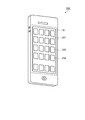
図14に示すように、第5の実施形態に係る電子機器(直視型の表示装置)としてのスマートフォン200は、携帯電話機能と、PDA(Personal Digital Assistant)機能とを兼ね備えた携帯端末装置である。また、通常の音声通話などの通信機能だけでなく、ネットワーク機能や、スケジュール・個人情報の管理などの電子手帳としての機能も備えている。
As shown in FIG. 14, a
スマートフォン200は、操作部兼表示部201に、上述した第3の実施形態の対向基板30Bを有する液晶装置1Bを備えている。操作部兼表示部201には、例えば、アイコン202が表示される。スマートフォン200では、アイコン202にタッチするなどの操作により種々の機能を動作させて、操作部兼表示部201に表示を行うことができる。
The
第5の実施形態に係るスマートフォン200の構成によれば、複数の画素P(P(R),P(G),P(B))が高精細に配置されていても、第3の実施形態の液晶装置1Bを備えているので、表示の明るさと表示品質とに優れたスマートフォン200を提供することができる。
According to the configuration of the
なお、液晶装置1Bを適用可能な電子機器は、スマートフォン200に限定されない。液晶装置1Bは、例えば、ディスプレイ、携帯電話機、PDA(Personal Digital Assistants)、モバイルコンピューター、デジタルスチルカメラ、デジタルビデオカメラ、カーナビゲーション装置、オーディオ機器などの直視型の表示装置にも好適に用いることができる。
The electronic device to which the
1,1A,1B…液晶装置(電気光学装置)、10…マイクロレンズアレイ基板(第1部材)、11…基板、11a…面、14…マイクロレンズ、20…素子基板(第1基板)、24…TFT(スイッチング素子)、28…画素電極、30,30A,30B…対向基板(電気光学装置用基板、第2基板)、31…光路長調整層(第2部材)、31a…表面、31b…溝、32…遮光層、32a…開口部、32b…表面、33…平坦化層(第2部材)、33a…表面、33b…溝、34…共通電極、40…液晶層(電気光学物質層)、60…プリズム基板(第1部材)、65…プリズム(反射部)、70…カラーフィルター基板(第1部材)、73,73R,73G,73B…カラーフィルター、100…プロジェクター(電子機器)、200…スマートフォン(電子機器)。
DESCRIPTION OF
Claims (7)
前記第1部材上に配置された第2部材と、
前記第2部材の表面側に設けられ、複数の画素の各々に対応する複数の開口部を有する遮光層と、
前記第2部材と前記遮光層とを覆うとともに、前記遮光層に接するように設けられた共通電極と、を備え、
前記遮光層は金属材料で構成されており、
前記共通電極の厚さは22nm以下であり、
前記第2部材の表面と前記遮光層の表面との間隔は、前記共通電極の厚さ以下であることを特徴とする電気光学装置用基板。 A first member;
A second member disposed on the first member;
A light shielding layer provided on the surface side of the second member and having a plurality of openings corresponding to each of the plurality of pixels;
A common electrode provided to cover the second member and the light shielding layer and to be in contact with the light shielding layer;
The light shielding layer is made of a metal material,
The common electrode has a thickness of 22 nm or less;
The electro-optical device substrate according to claim 1, wherein a distance between the surface of the second member and the surface of the light shielding layer is equal to or less than a thickness of the common electrode.
前記第2部材の前記表面には、前記複数の開口部のうちの隣り合う開口部の間に溝が設けられており、
前記遮光層は、前記溝の内部に設けられていることを特徴とする電気光学装置用基板。 The electro-optical device substrate according to claim 1,
A groove is provided on the surface of the second member between adjacent openings of the plurality of openings,
The substrate for an electro-optical device, wherein the light shielding layer is provided inside the groove.
前記第1部材には、前記複数の開口部の各々に対応してマイクロレンズが設けられていることを特徴とする電気光学装置用基板。 The substrate for an electro-optical device according to claim 1 or 2,
The electro-optical device substrate, wherein the first member is provided with a microlens corresponding to each of the plurality of openings.
前記第1部材には、前記複数の開口部のうちの隣り合う開口部の間に反射部が設けられていることを特徴とする電気光学装置用基板。 The substrate for an electro-optical device according to claim 1 or 2,
The electro-optical device substrate according to claim 1, wherein the first member is provided with a reflection portion between adjacent openings of the plurality of openings.
前記第1部材には、前記複数の開口部の各々に対応してカラーフィルターが設けられていることを特徴とする電気光学装置用基板。 The substrate for an electro-optical device according to claim 1 or 2,
The electro-optical device substrate according to claim 1, wherein the first member is provided with a color filter corresponding to each of the plurality of openings.
前記第1基板に対向配置された第2基板と、
前記第1基板と前記第2基板との間に配置された電気光学物質層と、を備え、
前記第2基板が、請求項1から5のいずれか一項に記載の電気光学装置用基板であることを特徴とする電気光学装置。 A first substrate provided with a plurality of pixel electrodes and a switching element corresponding to each of the plurality of pixel electrodes;
A second substrate disposed opposite the first substrate;
An electro-optic material layer disposed between the first substrate and the second substrate,
6. The electro-optical device, wherein the second substrate is the substrate for an electro-optical device according to any one of claims 1 to 5.
Priority Applications (1)
| Application Number | Priority Date | Filing Date | Title |
|---|---|---|---|
| JP2013016572A JP2014149335A (en) | 2013-01-31 | 2013-01-31 | Substrate for electro-optic device, electro-optic device, and electronic equipment |
Applications Claiming Priority (1)
| Application Number | Priority Date | Filing Date | Title |
|---|---|---|---|
| JP2013016572A JP2014149335A (en) | 2013-01-31 | 2013-01-31 | Substrate for electro-optic device, electro-optic device, and electronic equipment |
Publications (1)
| Publication Number | Publication Date |
|---|---|
| JP2014149335A true JP2014149335A (en) | 2014-08-21 |
Family
ID=51572380
Family Applications (1)
| Application Number | Title | Priority Date | Filing Date |
|---|---|---|---|
| JP2013016572A Pending JP2014149335A (en) | 2013-01-31 | 2013-01-31 | Substrate for electro-optic device, electro-optic device, and electronic equipment |
Country Status (1)
| Country | Link |
|---|---|
| JP (1) | JP2014149335A (en) |
Cited By (4)
| Publication number | Priority date | Publication date | Assignee | Title |
|---|---|---|---|---|
| KR20170056083A (en) * | 2015-11-12 | 2017-05-23 | 삼성디스플레이 주식회사 | Polarizer and display device having the same |
| JP2019522822A (en) * | 2016-08-08 | 2019-08-15 | 昆山龍騰光電有限公司 | Liquid crystal display device capable of switching viewing angle and method of switching viewing angle thereof |
| CN110764252A (en) * | 2019-10-28 | 2020-02-07 | 京东方科技集团股份有限公司 | Transparent panel and naked eye three-dimensional display device |
| WO2021014907A1 (en) * | 2019-07-19 | 2021-01-28 | ソニー株式会社 | Liquid crystal display device and electronic device |
-
2013
- 2013-01-31 JP JP2013016572A patent/JP2014149335A/en active Pending
Cited By (8)
| Publication number | Priority date | Publication date | Assignee | Title |
|---|---|---|---|---|
| KR20170056083A (en) * | 2015-11-12 | 2017-05-23 | 삼성디스플레이 주식회사 | Polarizer and display device having the same |
| KR102520245B1 (en) * | 2015-11-12 | 2023-04-11 | 삼성디스플레이 주식회사 | Polarizer and display device having the same |
| JP2019522822A (en) * | 2016-08-08 | 2019-08-15 | 昆山龍騰光電有限公司 | Liquid crystal display device capable of switching viewing angle and method of switching viewing angle thereof |
| US10809551B2 (en) | 2016-08-08 | 2020-10-20 | Infovision Optoelectronics (Kunshan) Co., Ltd. | Liquid crystal display device having switchable viewing angles and viewing angle switching method thereof |
| WO2021014907A1 (en) * | 2019-07-19 | 2021-01-28 | ソニー株式会社 | Liquid crystal display device and electronic device |
| US11927846B2 (en) | 2019-07-19 | 2024-03-12 | Sony Group Corporation | Liquid crystal display device and electronic apparatus |
| CN110764252A (en) * | 2019-10-28 | 2020-02-07 | 京东方科技集团股份有限公司 | Transparent panel and naked eye three-dimensional display device |
| CN110764252B (en) * | 2019-10-28 | 2022-02-25 | 京东方科技集团股份有限公司 | Transparent panel and naked eye three-dimensional display device |
Similar Documents
| Publication | Publication Date | Title |
|---|---|---|
| US9823530B2 (en) | Electro-optical apparatus and electronic apparatus | |
| JP6318881B2 (en) | Microlens array substrate, microlens array substrate manufacturing method, electro-optical device, and electronic apparatus | |
| JP6044358B2 (en) | Electro-optical device substrate, electro-optical device, and electronic apparatus | |
| JP2015011090A (en) | Method for manufacturing substrate for electro-optic device, substrate for electro-optic device, electro-optic device and electronic device | |
| JP2013025071A (en) | Electro-optic device, method for manufacturing electro-optic device, and projection type display device | |
| JP2012215747A (en) | Electro-optic device, electronic appliance, and manufacturing method for electro-optic device | |
| JP5948777B2 (en) | Liquid crystal device, method for manufacturing liquid crystal device, and electronic apparatus | |
| JP2014149335A (en) | Substrate for electro-optic device, electro-optic device, and electronic equipment | |
| JP2014092601A (en) | Method for manufacturing microlens array substrate, microlens array substrate, electro-optic device, and electronic equipment | |
| JP2014102268A (en) | Microlens array substrate, electro-optic device, and electronic equipment | |
| US20150077686A1 (en) | Substrate for electro-optical device, electro-optical device, and electronic apparatus | |
| JP6303283B2 (en) | Semiconductor device, electro-optical device, semiconductor device manufacturing method, and electronic apparatus | |
| JP6299493B2 (en) | Microlens array substrate, electro-optical device, and electronic device | |
| JP6032065B2 (en) | Method for manufacturing substrate for electro-optical device | |
| JP6028915B2 (en) | Electro-optical device manufacturing method, electro-optical device, and electronic apparatus | |
| JP6127500B2 (en) | Electro-optical device manufacturing method, electro-optical device, and electronic apparatus | |
| JP2014126574A (en) | Method for manufacturing substrate for electrooptical device, electro optical device and electronic equipment | |
| JP2016018094A (en) | Method for manufacturing substrate for electro-optic device, substrate for electro-optic device, electro-optic device, and electronic equipment | |
| US9383633B2 (en) | Electro-optical device and electronic apparatus | |
| JP6236827B2 (en) | Electro-optical device, method of manufacturing electro-optical device, and electronic apparatus | |
| JP2015094879A (en) | Manufacturing method for microlens array substrate, electro-optical device, and electronic device | |
| JP2014187240A (en) | Method for manufacturing substrate for electrooptical device, substrate for electrooptical device, electrooptical device, and electronic equipment | |
| JP2013025073A (en) | Electro-optic device, method for manufacturing electro-optic device, and projection type display device | |
| JP2013025070A (en) | Electro-optic device, method for manufacturing electro-optic device, and projection type display device | |
| JP2015087571A (en) | Method for manufacturing microlens array substrate, microlens array substrate, electro-optic device, and electronic equipment |
Legal Events
| Date | Code | Title | Description |
|---|---|---|---|
| RD04 | Notification of resignation of power of attorney |
Free format text: JAPANESE INTERMEDIATE CODE: A7424 Effective date: 20150109 |