JP2014107565A - Insulating layer conduction method - Google Patents
Insulating layer conduction method Download PDFInfo
- Publication number
- JP2014107565A JP2014107565A JP2013241744A JP2013241744A JP2014107565A JP 2014107565 A JP2014107565 A JP 2014107565A JP 2013241744 A JP2013241744 A JP 2013241744A JP 2013241744 A JP2013241744 A JP 2013241744A JP 2014107565 A JP2014107565 A JP 2014107565A
- Authority
- JP
- Japan
- Prior art keywords
- insulating layer
- bump
- diameter
- conduction method
- core
- Prior art date
- Legal status (The legal status is an assumption and is not a legal conclusion. Google has not performed a legal analysis and makes no representation as to the accuracy of the status listed.)
- Pending
Links
Images


Classifications
-
- H—ELECTRICITY
- H05—ELECTRIC TECHNIQUES NOT OTHERWISE PROVIDED FOR
- H05K—PRINTED CIRCUITS; CASINGS OR CONSTRUCTIONAL DETAILS OF ELECTRIC APPARATUS; MANUFACTURE OF ASSEMBLAGES OF ELECTRICAL COMPONENTS
- H05K3/00—Apparatus or processes for manufacturing printed circuits
- H05K3/46—Manufacturing multilayer circuits
- H05K3/4644—Manufacturing multilayer circuits by building the multilayer layer by layer, i.e. build-up multilayer circuits
- H05K3/4647—Manufacturing multilayer circuits by building the multilayer layer by layer, i.e. build-up multilayer circuits by applying an insulating layer around previously made via studs
-
- H—ELECTRICITY
- H05—ELECTRIC TECHNIQUES NOT OTHERWISE PROVIDED FOR
- H05K—PRINTED CIRCUITS; CASINGS OR CONSTRUCTIONAL DETAILS OF ELECTRIC APPARATUS; MANUFACTURE OF ASSEMBLAGES OF ELECTRICAL COMPONENTS
- H05K2203/00—Indexing scheme relating to apparatus or processes for manufacturing printed circuits covered by H05K3/00
- H05K2203/02—Details related to mechanical or acoustic processing, e.g. drilling, punching, cutting, using ultrasound
- H05K2203/025—Abrading, e.g. grinding or sand blasting
-
- H—ELECTRICITY
- H05—ELECTRIC TECHNIQUES NOT OTHERWISE PROVIDED FOR
- H05K—PRINTED CIRCUITS; CASINGS OR CONSTRUCTIONAL DETAILS OF ELECTRIC APPARATUS; MANUFACTURE OF ASSEMBLAGES OF ELECTRICAL COMPONENTS
- H05K2203/00—Indexing scheme relating to apparatus or processes for manufacturing printed circuits covered by H05K3/00
- H05K2203/04—Soldering or other types of metallurgic bonding
- H05K2203/049—Wire bonding
-
- H—ELECTRICITY
- H05—ELECTRIC TECHNIQUES NOT OTHERWISE PROVIDED FOR
- H05K—PRINTED CIRCUITS; CASINGS OR CONSTRUCTIONAL DETAILS OF ELECTRIC APPARATUS; MANUFACTURE OF ASSEMBLAGES OF ELECTRICAL COMPONENTS
- H05K3/00—Apparatus or processes for manufacturing printed circuits
- H05K3/40—Forming printed elements for providing electric connections to or between printed circuits
- H05K3/4038—Through-connections; Vertical interconnect access [VIA] connections
- H05K3/4046—Through-connections; Vertical interconnect access [VIA] connections using auxiliary conductive elements, e.g. metallic spheres, eyelets, pieces of wire
-
- H—ELECTRICITY
- H05—ELECTRIC TECHNIQUES NOT OTHERWISE PROVIDED FOR
- H05K—PRINTED CIRCUITS; CASINGS OR CONSTRUCTIONAL DETAILS OF ELECTRIC APPARATUS; MANUFACTURE OF ASSEMBLAGES OF ELECTRICAL COMPONENTS
- H05K3/00—Apparatus or processes for manufacturing printed circuits
- H05K3/46—Manufacturing multilayer circuits
- H05K3/4644—Manufacturing multilayer circuits by building the multilayer layer by layer, i.e. build-up multilayer circuits
- H05K3/4673—Application methods or materials of intermediate insulating layers not specially adapted to any one of the previous methods of adding a circuit layer
Abstract
Description
本発明は、絶縁層の導通方法に関し、より詳細には、絶縁層の層間をバンプによって導通させる絶縁層の導通方法に関する。 The present invention relates to a method for conducting an insulating layer, and more particularly to a method for conducting an insulating layer in which layers between the insulating layers are made conductive by bumps.
最近、電子部品の小型化、多機能化の傾向により、既存に用いられていたプリント回路基板においてもパターン微細化、高集的の薄型製品に対する要求が高まっている。 Recently, due to the trend toward miniaturization and multi-functionality of electronic components, there is an increasing demand for pattern miniaturization and highly concentrated thin products even in existing printed circuit boards.
現在、多層回路基板において一般的に積層される層間を導通させる方法は、レーザドリルを用いて絶縁層にホールを形成した後、内部を銅でメッキする方法である。 At present, a method of conducting between layers generally laminated in a multilayer circuit board is a method of forming a hole in an insulating layer using a laser drill and then plating the inside with copper.
電子機器の高性能化はより速い応答速度を意味し、高性能化の実現により、電子機器から発生する発熱が増加しつつある。 Higher performance of electronic devices means faster response speed, and heat generation generated from electronic devices is increasing due to higher performance.
このような発熱の増加によって基板の反りが問題となっており、基板の反り問題を解消するために、絶縁材の材料を低い熱膨張係数を有する素材に代替するための検討が持続的に行われている。 The warpage of the substrate has become a problem due to such an increase in heat generation, and in order to solve the problem of the warpage of the substrate, investigations for replacing the insulating material with a material having a low coefficient of thermal expansion are continuously conducted. It has been broken.
通常、絶縁材材料の熱膨張係数を低めるためには、絶縁材のフィラー(Filler)の含量またはガラスクロス(Glass Cloth)の含量を増加させる。 Usually, in order to reduce the thermal expansion coefficient of the insulating material, the filler content or glass cloth content of the insulating material is increased.
レーザドリル加工は、レーザパワーを用いて絶縁材の高分子化合物と無機材料であるフィラーまたはガラスクロスを除去することである。 Laser drilling is to remove a polymer compound of an insulating material and a filler or glass cloth, which is an inorganic material, using laser power.
しかし、フィラーの含量またはガラスクロスの含量が増加すると、レーザドリル加工によるホールの形成時に除去しなければならない無機材料成分であるフィラーとガラスクロスも増加するため、より高いレーザパワーが要されたり、レーザ加工時間が増加したりするなど、レーザ加工が困難となり、工程コストが上昇するという問題点がある。 However, as the filler content or glass cloth content increases, the filler and glass cloth, which are inorganic material components that must be removed when forming holes by laser drilling, also increase, so higher laser power is required, There is a problem that the laser processing becomes difficult and the process cost increases, such as an increase in laser processing time.
本発明は上記の問題点に鑑みてなされたものであり、多重積層された絶縁層の層間を、レーザを用いずバンプによって導通させることにより、工数の低減及びパッケージ基板の信頼性の増大を期待することができる、絶縁層の導通方法を提供することを目的とする。 The present invention has been made in view of the above-mentioned problems, and is expected to reduce man-hours and increase the reliability of the package substrate by connecting the layers of the multi-layered insulating layers with bumps without using a laser. It is an object of the present invention to provide a method for conducting an insulating layer that can be performed.
上記の目的を効果的に果たすために、本発明は、硬質の絶縁層を提供する段階と、前記絶縁層にランドを形成する段階と、前記ランドにバンプを形成する段階と、前記バンプによって貫通される軟質の絶縁層を前記硬質の絶縁層に積層する段階と、前記積層された軟質の絶縁層を硬化する段階と、前記絶縁層とバンプの上面を研磨機で加工する段階と、を含むことができる。 In order to effectively achieve the above object, the present invention provides a step of providing a hard insulating layer, a step of forming a land on the insulating layer, a step of forming a bump on the land, and a penetration by the bump. Laminating the soft insulating layer to be formed on the hard insulating layer, curing the laminated soft insulating layer, and processing the upper surface of the insulating layer and the bump with a polishing machine. be able to.
前記バンプを形成する段階は、前記ランドにワイヤをボンディングした後、前記ワイヤを切断することによりなされることができる。 The step of forming the bump may be performed by bonding the wire to the land and then cutting the wire.
この際、前記バンプは、上部の直径より下部の直径が広い瓢箪形状を有することができ、前記バンプは、上部の直径が20μm以内であり、下部の直径が25μm〜35μmの範囲を満たすことができる。 In this case, the bump may have a bowl shape having a lower diameter wider than an upper diameter, and the bump has an upper diameter of 20 μm or less and a lower diameter satisfying a range of 25 μm to 35 μm. it can.
また、前記バンプは、上部及び下部の直径より中央部位の直径が広い樽形状を有することもできる。 In addition, the bump may have a barrel shape in which the diameter of the central portion is wider than the diameter of the upper and lower portions.
一方、本発明は、第2実施形態として、コアが形成された硬質の絶縁層を提供する段階と、前記絶縁層のコアの両端部にランドをそれぞれ形成する段階と、前記ランドにバンプを形成する段階と、前記バンプの上端によって貫通される軟質の絶縁層を前記硬質の絶縁層に積層する段階と、前記積層された軟質の絶縁層を硬化する段階と、前記絶縁層とバンプの上端部を研磨機で加工する段階と、を含むことができる。 On the other hand, the present invention provides, as a second embodiment, a step of providing a hard insulating layer having a core formed thereon, a step of forming lands on both ends of the core of the insulating layer, and a step of forming bumps on the lands. Laminating a soft insulating layer penetrating the upper end of the bump on the hard insulating layer, curing the laminated soft insulating layer, and an upper end portion of the insulating layer and the bump Processing with a polishing machine.
前記バンプを形成する段階は、前記ランドにワイヤをボンディングした後、前記ワイヤを切断することによりなされることができる。 The step of forming the bump may be performed by bonding the wire to the land and then cutting the wire.
また、前記バンプは、上部の直径より下部の直径が広い瓢箪形状を有することができ、前記バンプは、上部の直径が20μm以内であり、下部の直径が25μm〜35μmの範囲を満たすことができる。 The bump may have a bowl shape having a lower diameter wider than an upper diameter, and the bump may have an upper diameter of 20 μm or less and a lower diameter of 25 μm to 35 μm. .
この際、前記バンプは、上部及び下部の直径より中央部位の直径が広い樽形状を有することができる。 At this time, the bump may have a barrel shape in which the diameter of the central portion is wider than the diameter of the upper and lower portions.
また、前記コアは、硬質の絶縁層にコアホールを形成した後、前記コアホールにメッキ層を充填することにより形成されることができ、前記コアホールは、レーザ加工または機械ドリル加工のうち何れか一つの加工により形成されることができる。 The core may be formed by forming a core hole in a hard insulating layer and then filling the core hole with a plating layer. The core hole may be formed by laser processing or mechanical drilling. It can be formed by one process.
本発明の実施形態による絶縁層の導通方法は、多重積層された絶縁層の層間を、レーザを用いずバンプによって導通させることにより、工数の低減及びパッケージ基板の信頼性の増大を期待することができる効果がある。 The insulating layer conduction method according to the embodiment of the present invention can be expected to reduce man-hours and increase the reliability of the package substrate by conducting conduction between the layers of the laminated insulating layers by bumps without using a laser. There is an effect that can be done.
以下、本発明の実施形態による絶縁層の導通方法を添付図面を参照して詳細に説明すると、次のとおりである。 Hereinafter, a conduction method of an insulating layer according to an embodiment of the present invention will be described in detail with reference to the accompanying drawings.
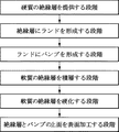
図1aから図1eは本発明の絶縁層の導通方法によって絶縁層が導通される過程を示す例示図であり、図2は本発明の絶縁層の導通方法によって絶縁層が導通された状態を示す例示図であり、図3は本発明の絶縁層の導通方法によって絶縁層が導通される過程を示すフローチャートであり、図4は本発明の絶縁層の導通方法によってコアが形成された絶縁層に絶縁層が積層された状態を示す例示図であり、図5は図4を構成するための工程手順を示すフローチャートである。 FIGS. 1a to 1e are exemplary diagrams illustrating a process in which an insulating layer is conducted by the insulating layer conduction method of the present invention, and FIG. 2 illustrates a state in which the insulating layer is conducted by the insulating layer conduction method of the present invention. FIG. 3 is a flowchart illustrating a process in which the insulating layer is conducted by the insulating layer conduction method of the present invention. FIG. 4 is a flowchart illustrating the process of forming the core in the insulating layer conduction method of the present invention. FIG. 5 is an exemplary diagram showing a state in which insulating layers are laminated, and FIG. 5 is a flowchart showing a process procedure for configuring FIG.
図1から図3に図示されたように、本発明の実施形態による絶縁層の導通方法は、硬質の絶縁層10を基準として両側に軟質の絶縁層40を積層する場合と、硬質の絶縁層10に軟質の絶縁層40を順に積層する場合の両方に適用されることができる。
As shown in FIGS. 1 to 3, the insulating layer conduction method according to the embodiment of the present invention includes a case where a
本発明による絶縁層の導通方法について説明すると、次のとおりである。 The conduction method of the insulating layer according to the present invention will be described as follows.
まず、硬質の絶縁層10を提供した後、絶縁層10にランド20を形成する。ランド20は、優れた電気的特性を有する銅が好ましく用いられることができるが、回路パターンの設計事項によってその位置が変わることができる。
First, after providing the hard insulating
硬質の絶縁層10にランド20が形成されると、ランド20の表面にバンプ30を形成する。バンプ30は、ワイヤボンディングの原理を利用したものであって、ワイヤの端部をランド20の表面に圧着した後、圧着された端部から所定長さの部分を切断することにより形成されることができる。
When the
ランド20に形成されたバンプ30の形状は、上部32の直径と下部34の直径が異なることができる。これは、ワイヤがランド20の表面に圧着される過程でワイヤの端部に加えられる荷重によってランド20の表面との接触面積が広くなるためである。
As for the shape of the
従って、バンプ30は、上部32の直径より下部34の直径が広い瓢箪形状を有することができる。
Accordingly, the
この際、バンプの上部32の直径は20μm以内であり、下部34の直径は25μm〜35μmの範囲を満たすことができる。
At this time, the diameter of the
バンプの上部32の直径はワイヤの直径に相当し、より大きい直径を有するワイヤを用いる場合、バンプの上部32の直径も変更されるということは勿論である。
The diameter of the
また、バンプの下部34の直径は、ランド20の上部に加えられる荷重の大きさによって変わることができる。
Further, the diameter of the
換言すれば、ワイヤの端部によりランド20の表面に加えられる荷重が大きい場合にはバンプの下部34の直径がより大きくなり、反対に荷重が小さい場合にはバンプの下部34の直径がより小さくなる。
In other words, when the load applied to the surface of the
しかし、本発明では、バンプ30を形成するにあたり、上部32と下部34の直径をそれぞれ20μm以内と25μm〜35μmの範囲となるように形成する場合に、最も好ましいバンプ30の形状が得られた。
However, in the present invention, when the
従って、バンプ30は、ランド20の表面に加えられる荷重の大きさによって、瓢箪形状または図面には図示していないが樽形状などに形成されることができる。
Therefore, the
このような工程を経てランド20にバンプ30が形成されると、軟質の絶縁層40を硬質の絶縁層10に積層する。
When the
即ち、軟質の絶縁層40は、バンプの上部32によって貫通されながら硬質の絶縁層10に積層される。
That is, the soft insulating
この際、軟質の絶縁層40を硬質の絶縁層10に積層する過程で、硬質の絶縁層10がバンプの上部32によって貫通されていない状態で、軟質の絶縁層40を硬化する工程を行うこともできる。
At this time, in the process of laminating the soft insulating
換言すれば、軟質の絶縁層40を硬質の絶縁層10に積層する過程で、バンプの上部32が鋭くない場合、軟質の絶縁層40が貫通されていない状態でバンプの上部32に掛けられる形態で積層されることができる。
In other words, in the process of laminating the soft insulating
この場合にも、軟質の絶縁層40をそのまま維持した状態で硬化過程を行うことができる。
Also in this case, the curing process can be performed with the soft insulating
軟質の絶縁層40の硬化工程は、熱硬化方法、化学品を塗布して行う化学硬化方法、UVなどの光を用いて行う光硬化方法など、様々な硬化方法のうち何れか一つの方法により行われる。
The curing process of the soft insulating
このような硬化方法によって軟質の絶縁層40が硬化されると、硬化された絶縁層とバンプの上部32を研磨機Yで表面加工する。
When the soft insulating
表面加工は、硬化された絶縁層の上部の表面が平坦化されるように、硬化された絶縁層とバンプの上部32を同時に研磨することによりなされる。
The surface processing is performed by simultaneously polishing the hardened insulating layer and the
この際、バンプの上部32に掛けられた軟質の絶縁層40は、バンプの上部32の高さが非常に低い状態であるため、表面加工過程を経て硬化された絶縁層とバンプの上部32を同時に除去した後、硬化された絶縁層を押して硬質の絶縁層10と密着させる。
At this time, since the soft insulating
このように表面加工が完了すると、硬化された絶縁層の上部にランド20を形成し、ランド20にバンプ30を形成した後、表面加工を施す過程を繰り返して行う。
When the surface processing is completed as described above, the
従って、本発明による絶縁層の導通方法を行う場合、層間導通のためにレーザまたはドリルを用いてビアホールを形成したり、ビアホールの内部にシード層及びメッキ層を形成したりする工程を省略することができるため、作業工数を低減し、生産性の向上を期待することができる。 Therefore, when performing the insulating layer conduction method according to the present invention, a step of forming a via hole using a laser or a drill for interlayer conduction or forming a seed layer and a plating layer inside the via hole is omitted. Therefore, it is possible to reduce the work man-hours and improve productivity.
一方、本発明による絶縁層の導通方法は、図4及び図5に図示されたように、コア12が形成された硬質の絶縁層10を基準として軟質の絶縁層40が積層される形態に適用されることもできる。
On the other hand, the insulating layer conduction method according to the present invention is applied to a configuration in which a soft insulating
コア12が形成された硬質の絶縁層10は、コア12を硬質の絶縁層10に形成するために、まず、絶縁層10にレーザまたはドリルを用いてコアホール14を形成する。
In the hard insulating
コアホール14は、回路パターンの設計によってその位置が決定され、垂直に貫通されることができる。
The position of the
コアホール14の内部にメッキを充填することによりコアホール14の内部を満たしてメッキ層を形成する。このようにコアホール14の内部にメッキ層が形成された後、硬質の絶縁層10の上部と下部に表面研磨を施すことができる。
By filling the inside of the
この際、コア12の高さは0.2〜0.4mm程度に形成されることができるが、これは、硬質の絶縁層10の厚さによって多少変更され得る。
At this time, the height of the core 12 can be formed to about 0.2 to 0.4 mm, but this can be changed to some extent depending on the thickness of the hard insulating
このようにコア12が硬質の絶縁層10に形成されると、コア12の両側にランド20を形成することができる。ここで、コア12にランド20を形成することは、コア12の両側に同時に行われるのでなく、両側のうち一側に先に行われた後、反対側に行われることができる。
When the
ランド20は、コア12の直径より広い直径に形成されることができる。ランド20は、コアと電気的に導通されるように、コア12と同一の金属で形成されることができる。
The
コア12の両側にランド20が形成されると、ランド20に上述の工程によりバンプ30を形成した後、軟質の絶縁層40を硬質の絶縁層10に積層する。
When the
次に、軟質の絶縁層40を硬化した後、表面加工する過程を繰り返して行うことにより、多数の絶縁層40を積層することができる。
Next, after the soft insulating
上記のように、本発明の実施形態による絶縁層の導通方法は、絶縁層にコアが形成された場合やコアが形成されていない場合の両方とも、バンプによる絶縁層の導通が可能である。 As described above, the insulating layer conduction method according to the embodiment of the present invention enables conduction of the insulating layer by the bump both when the core is formed in the insulating layer and when the core is not formed.
以上、本発明の実施形態による絶縁層の導通方法について説明したが、本発明はこれに限定されず、当業者であればその応用及び変形が可能であるということがいうまでもない。 As mentioned above, although the conduction | electrical_connection method of the insulating layer by embodiment of this invention was demonstrated, this invention is not limited to this, It cannot be overemphasized that the application and deformation | transformation are possible for those skilled in the art.
10 硬質の絶縁層
12 コア
14 コアホール
20 ランド
30 バンプ
32 バンプの上部
34 バンプの下部
40 軟質の絶縁層
Y 研磨機
DESCRIPTION OF
Claims (12)
前記絶縁層にランドを形成する段階と、
前記ランドにバンプを形成する段階と、
前記バンプによって貫通される軟質の絶縁層を前記硬質の絶縁層に積層する段階と、
前記積層された軟質の絶縁層を硬化する段階と、
前記絶縁層とバンプの上面を研磨機で加工する段階と、を含む絶縁層の導通方法。 Providing a hard insulating layer;
Forming lands in the insulating layer;
Forming bumps on the lands;
Laminating a soft insulating layer penetrated by the bumps on the hard insulating layer;
Curing the laminated soft insulating layer;
And processing the upper surface of the insulating layer and the bump with a polishing machine.
前記絶縁層のコアの両端部にランドをそれぞれ形成する段階と、
前記ランドにバンプを形成する段階と、
前記バンプの上端によって貫通される軟質の絶縁層を前記硬質の絶縁層に積層する段階と、
前記積層された軟質の絶縁層を硬化する段階と、
前記絶縁層とバンプの上端部を研磨機で加工する段階と、を含む絶縁層の導通方法。 Providing a hard insulating layer with a core formed thereon;
Forming lands on both ends of the core of the insulating layer,
Forming bumps on the lands;
Laminating a soft insulating layer penetrated by the upper end of the bump on the hard insulating layer;
Curing the laminated soft insulating layer;
Processing the insulating layer and the upper end of the bump with a polishing machine.
Applications Claiming Priority (2)
| Application Number | Priority Date | Filing Date | Title |
|---|---|---|---|
| KR10-2012-0135348 | 2012-11-27 | ||
| KR1020120135348A KR20140067723A (en) | 2012-11-27 | 2012-11-27 | Current method of lamination pcb |
Publications (1)
| Publication Number | Publication Date |
|---|---|
| JP2014107565A true JP2014107565A (en) | 2014-06-09 |
Family
ID=50772223
Family Applications (1)
| Application Number | Title | Priority Date | Filing Date |
|---|---|---|---|
| JP2013241744A Pending JP2014107565A (en) | 2012-11-27 | 2013-11-22 | Insulating layer conduction method |
Country Status (3)
| Country | Link |
|---|---|
| US (1) | US20140144575A1 (en) |
| JP (1) | JP2014107565A (en) |
| KR (1) | KR20140067723A (en) |
Families Citing this family (1)
| Publication number | Priority date | Publication date | Assignee | Title |
|---|---|---|---|---|
| US10177131B2 (en) | 2016-03-02 | 2019-01-08 | Samsung Electronics Co., Ltd. | Semiconductor packages and methods of manufacturing the same |
Citations (5)
| Publication number | Priority date | Publication date | Assignee | Title |
|---|---|---|---|---|
| JPH10135218A (en) * | 1996-10-29 | 1998-05-22 | Taiyo Yuden Co Ltd | Bump and forming method thereof |
| JP2001244591A (en) * | 2001-02-06 | 2001-09-07 | Ngk Spark Plug Co Ltd | Wiring board and manufacturing method thereof |
| JP2002141370A (en) * | 2000-11-02 | 2002-05-17 | Matsushita Electric Ind Co Ltd | Semiconductor device, method and apparatus for manufacturing the same as well as method for mounting semiconductor device |
| JP2003298236A (en) * | 2002-03-29 | 2003-10-17 | Matsushita Electric Ind Co Ltd | Multilayer wiring board and method and device for manufacturing the same |
| JP2007281480A (en) * | 2006-04-11 | 2007-10-25 | Samsung Electro-Mechanics Co Ltd | Printed-circuit board using bump, and its manufacturing method |
Family Cites Families (8)
| Publication number | Priority date | Publication date | Assignee | Title |
|---|---|---|---|---|
| JP3421548B2 (en) * | 1997-09-10 | 2003-06-30 | 富士通株式会社 | Semiconductor bare chip, semiconductor bare chip manufacturing method, and semiconductor bare chip mounting structure |
| US6063647A (en) * | 1997-12-08 | 2000-05-16 | 3M Innovative Properties Company | Method for making circuit elements for a z-axis interconnect |
| JP3137186B2 (en) * | 1999-02-05 | 2001-02-19 | インターナショナル・ビジネス・マシーンズ・コーポレ−ション | Interlayer connection structure, multilayer wiring board, and method for forming them |
| JP2001093938A (en) * | 1999-09-20 | 2001-04-06 | Nec Kansai Ltd | Semiconductor device and its manufacturing method |
| JP4048019B2 (en) * | 2000-08-31 | 2008-02-13 | 富士通株式会社 | Multilayer wiring board and manufacturing method thereof |
| CN100553410C (en) * | 2001-03-28 | 2009-10-21 | 德塞拉互连材料股份有限公司 | The metallic plate of multi-layer wire substrate, multi-layer wire substrate manufacture method, multi-layer wire substrate grinder and manufacturing circuit board |
| US7631423B2 (en) * | 2006-02-13 | 2009-12-15 | Sanmina-Sci Corporation | Method and process for embedding electrically conductive elements in a dielectric layer |
| JP5497392B2 (en) * | 2009-09-25 | 2014-05-21 | ルネサスエレクトロニクス株式会社 | Semiconductor device |
-
2012
- 2012-11-27 KR KR1020120135348A patent/KR20140067723A/en not_active Application Discontinuation
-
2013
- 2013-11-22 JP JP2013241744A patent/JP2014107565A/en active Pending
- 2013-11-26 US US14/091,156 patent/US20140144575A1/en not_active Abandoned
Patent Citations (5)
| Publication number | Priority date | Publication date | Assignee | Title |
|---|---|---|---|---|
| JPH10135218A (en) * | 1996-10-29 | 1998-05-22 | Taiyo Yuden Co Ltd | Bump and forming method thereof |
| JP2002141370A (en) * | 2000-11-02 | 2002-05-17 | Matsushita Electric Ind Co Ltd | Semiconductor device, method and apparatus for manufacturing the same as well as method for mounting semiconductor device |
| JP2001244591A (en) * | 2001-02-06 | 2001-09-07 | Ngk Spark Plug Co Ltd | Wiring board and manufacturing method thereof |
| JP2003298236A (en) * | 2002-03-29 | 2003-10-17 | Matsushita Electric Ind Co Ltd | Multilayer wiring board and method and device for manufacturing the same |
| JP2007281480A (en) * | 2006-04-11 | 2007-10-25 | Samsung Electro-Mechanics Co Ltd | Printed-circuit board using bump, and its manufacturing method |
Also Published As
| Publication number | Publication date |
|---|---|
| US20140144575A1 (en) | 2014-05-29 |
| KR20140067723A (en) | 2014-06-05 |
Similar Documents
| Publication | Publication Date | Title |
|---|---|---|
| TWI553792B (en) | Package structure and manufacturing method thereof | |
| KR101516072B1 (en) | Semiconductor Package and Method of Manufacturing The Same | |
| JP6795137B2 (en) | Manufacturing method of printed circuit board with built-in electronic elements | |
| JP2013033894A5 (en) | ||
| TW201533872A (en) | Semiconductor apparatus and method for fabricating the same | |
| CN104540338A (en) | Manufacturing method of high-alignment HDI (High Density Interconnection) product | |
| JP2014096581A (en) | Circuit board and method for manufacturing the same | |
| KR20150064976A (en) | Printed circuit board and manufacturing method thereof | |
| KR101104210B1 (en) | Electro device embedded printed circuit board and manufacturing method thereof | |
| US20080230264A1 (en) | Interconnection structure and method thereof | |
| JP2017011075A (en) | Electronic component device and method of manufacturing the same | |
| JP6511851B2 (en) | Multilayer circuit board, semiconductor device, method of manufacturing multilayer circuit board | |
| JP2015198094A (en) | Interposer, semiconductor device, and method of manufacturing them | |
| JP2014022715A (en) | Coreless substrate and method of manufacturing the same | |
| TW201603672A (en) | Method for forming a via structure using a double-side laser process | |
| CN104703399A (en) | Circuit board and production method thereof | |
| JP2014107565A (en) | Insulating layer conduction method | |
| WO2017020448A1 (en) | Method for mechanically preparing via hole on printed circuit board and printed circuit board with mechanically prepared via hole | |
| KR102141102B1 (en) | Method for manufacturing semiconductor package substrate and semiconductor package substrate manufactured using the same | |
| TWI566330B (en) | Method of fabricating an electronic package structure | |
| KR102130757B1 (en) | Method for manufacturing semiconductor package substrate and semiconductor package substrate manufactured using the same | |
| KR20070007406A (en) | Printed circuit board with embedded coaxial cable and manufacturing method thereof | |
| KR102149797B1 (en) | Substrate and manufacturing method thereof | |
| US20080212287A1 (en) | Semiconductor package structure with buried electronic device and manufacturing method therof | |
| JP2013161951A (en) | Wiring board and method for manufacturing the same |
Legal Events
| Date | Code | Title | Description |
|---|---|---|---|
| A621 | Written request for application examination |
Free format text: JAPANESE INTERMEDIATE CODE: A621 Effective date: 20151215 |
|
| A977 | Report on retrieval |
Free format text: JAPANESE INTERMEDIATE CODE: A971007 Effective date: 20161110 |
|
| A131 | Notification of reasons for refusal |
Free format text: JAPANESE INTERMEDIATE CODE: A131 Effective date: 20161115 |
|
| A02 | Decision of refusal |
Free format text: JAPANESE INTERMEDIATE CODE: A02 Effective date: 20170613 |