JP2013243340A - Electronic component, mounting member, electronic apparatus, and manufacturing method of these - Google Patents
Electronic component, mounting member, electronic apparatus, and manufacturing method of these Download PDFInfo
- Publication number
- JP2013243340A JP2013243340A JP2013039450A JP2013039450A JP2013243340A JP 2013243340 A JP2013243340 A JP 2013243340A JP 2013039450 A JP2013039450 A JP 2013039450A JP 2013039450 A JP2013039450 A JP 2013039450A JP 2013243340 A JP2013243340 A JP 2013243340A
- Authority
- JP
- Japan
- Prior art keywords
- electronic device
- frame
- step portion
- base
- electronic component
- Prior art date
- Legal status (The legal status is an assumption and is not a legal conclusion. Google has not performed a legal analysis and makes no representation as to the accuracy of the status listed.)
- Pending
Links
- 238000004519 manufacturing process Methods 0.000 title claims description 19
- 239000000758 substrate Substances 0.000 claims abstract description 38
- 239000000853 adhesive Substances 0.000 claims description 99
- 230000001070 adhesive effect Effects 0.000 claims description 98
- 239000000463 material Substances 0.000 claims description 88
- 238000000034 method Methods 0.000 claims description 25
- 239000000919 ceramic Substances 0.000 claims description 19
- 229910052751 metal Inorganic materials 0.000 claims description 16
- 239000002184 metal Substances 0.000 claims description 16
- 230000008569 process Effects 0.000 claims description 11
- 239000012798 spherical particle Substances 0.000 claims description 4
- 238000005476 soldering Methods 0.000 claims description 3
- 230000003746 surface roughness Effects 0.000 claims description 3
- 229920005989 resin Polymers 0.000 description 25
- 239000011347 resin Substances 0.000 description 25
- 239000004020 conductor Substances 0.000 description 18
- 229920001187 thermosetting polymer Polymers 0.000 description 13
- 238000003384 imaging method Methods 0.000 description 11
- 230000002093 peripheral effect Effects 0.000 description 9
- 230000006870 function Effects 0.000 description 8
- 238000010586 diagram Methods 0.000 description 7
- 230000003287 optical effect Effects 0.000 description 7
- PXHVJJICTQNCMI-UHFFFAOYSA-N Nickel Chemical compound [Ni] PXHVJJICTQNCMI-UHFFFAOYSA-N 0.000 description 6
- 229910000679 solder Inorganic materials 0.000 description 6
- 239000011521 glass Substances 0.000 description 5
- PCHJSUWPFVWCPO-UHFFFAOYSA-N gold Chemical compound [Au] PCHJSUWPFVWCPO-UHFFFAOYSA-N 0.000 description 5
- 239000007788 liquid Substances 0.000 description 5
- 239000004065 semiconductor Substances 0.000 description 5
- 125000006850 spacer group Chemical group 0.000 description 5
- PNEYBMLMFCGWSK-UHFFFAOYSA-N aluminium oxide Inorganic materials [O-2].[O-2].[O-2].[Al+3].[Al+3] PNEYBMLMFCGWSK-UHFFFAOYSA-N 0.000 description 4
- 239000011248 coating agent Substances 0.000 description 4
- 238000000576 coating method Methods 0.000 description 4
- 229910000640 Fe alloy Inorganic materials 0.000 description 3
- 230000009471 action Effects 0.000 description 3
- 230000008901 benefit Effects 0.000 description 3
- 230000000052 comparative effect Effects 0.000 description 3
- 238000001723 curing Methods 0.000 description 3
- 238000010304 firing Methods 0.000 description 3
- 238000010438 heat treatment Methods 0.000 description 3
- 238000005304 joining Methods 0.000 description 3
- 238000010030 laminating Methods 0.000 description 3
- 239000007769 metal material Substances 0.000 description 3
- 229910052759 nickel Inorganic materials 0.000 description 3
- 238000000016 photochemical curing Methods 0.000 description 3
- 238000004080 punching Methods 0.000 description 3
- 238000007650 screen-printing Methods 0.000 description 3
- 229910001220 stainless steel Inorganic materials 0.000 description 3
- 238000012360 testing method Methods 0.000 description 3
- 238000011179 visual inspection Methods 0.000 description 3
- 229910000838 Al alloy Inorganic materials 0.000 description 2
- VYZAMTAEIAYCRO-UHFFFAOYSA-N Chromium Chemical compound [Cr] VYZAMTAEIAYCRO-UHFFFAOYSA-N 0.000 description 2
- XEEYBQQBJWHFJM-UHFFFAOYSA-N Iron Chemical compound [Fe] XEEYBQQBJWHFJM-UHFFFAOYSA-N 0.000 description 2
- MCMNRKCIXSYSNV-UHFFFAOYSA-N Zirconium dioxide Chemical compound O=[Zr]=O MCMNRKCIXSYSNV-UHFFFAOYSA-N 0.000 description 2
- 229910045601 alloy Inorganic materials 0.000 description 2
- 239000000956 alloy Substances 0.000 description 2
- 229910052782 aluminium Inorganic materials 0.000 description 2
- XAGFODPZIPBFFR-UHFFFAOYSA-N aluminium Chemical compound [Al] XAGFODPZIPBFFR-UHFFFAOYSA-N 0.000 description 2
- 239000002131 composite material Substances 0.000 description 2
- 230000000694 effects Effects 0.000 description 2
- 230000008020 evaporation Effects 0.000 description 2
- 238000001704 evaporation Methods 0.000 description 2
- 238000007689 inspection Methods 0.000 description 2
- 239000012212 insulator Substances 0.000 description 2
- 150000002739 metals Chemical class 0.000 description 2
- 238000011417 postcuring Methods 0.000 description 2
- 238000003825 pressing Methods 0.000 description 2
- 238000007639 printing Methods 0.000 description 2
- 238000012545 processing Methods 0.000 description 2
- 238000005488 sandblasting Methods 0.000 description 2
- 239000007787 solid Substances 0.000 description 2
- 238000007711 solidification Methods 0.000 description 2
- 230000008023 solidification Effects 0.000 description 2
- 229920001342 Bakelite® Polymers 0.000 description 1
- RYGMFSIKBFXOCR-UHFFFAOYSA-N Copper Chemical compound [Cu] RYGMFSIKBFXOCR-UHFFFAOYSA-N 0.000 description 1
- 229910000881 Cu alloy Inorganic materials 0.000 description 1
- 239000004593 Epoxy Substances 0.000 description 1
- 239000004642 Polyimide Substances 0.000 description 1
- 229910052581 Si3N4 Inorganic materials 0.000 description 1
- 230000001154 acute effect Effects 0.000 description 1
- 229910000963 austenitic stainless steel Inorganic materials 0.000 description 1
- 239000004637 bakelite Substances 0.000 description 1
- 229910010293 ceramic material Inorganic materials 0.000 description 1
- 239000011195 cermet Substances 0.000 description 1
- 238000006757 chemical reactions by type Methods 0.000 description 1
- 229910052804 chromium Inorganic materials 0.000 description 1
- 239000011651 chromium Substances 0.000 description 1
- 229910017052 cobalt Inorganic materials 0.000 description 1
- 239000010941 cobalt Substances 0.000 description 1
- GUTLYIVDDKVIGB-UHFFFAOYSA-N cobalt atom Chemical compound [Co] GUTLYIVDDKVIGB-UHFFFAOYSA-N 0.000 description 1
- 238000004891 communication Methods 0.000 description 1
- 230000008602 contraction Effects 0.000 description 1
- 239000010949 copper Substances 0.000 description 1
- 229910052802 copper Inorganic materials 0.000 description 1
- PMHQVHHXPFUNSP-UHFFFAOYSA-M copper(1+);methylsulfanylmethane;bromide Chemical compound Br[Cu].CSC PMHQVHHXPFUNSP-UHFFFAOYSA-M 0.000 description 1
- 229910052878 cordierite Inorganic materials 0.000 description 1
- 238000005260 corrosion Methods 0.000 description 1
- 230000007797 corrosion Effects 0.000 description 1
- 239000006071 cream Substances 0.000 description 1
- 238000005520 cutting process Methods 0.000 description 1
- 230000001419 dependent effect Effects 0.000 description 1
- JSKIRARMQDRGJZ-UHFFFAOYSA-N dimagnesium dioxido-bis[(1-oxido-3-oxo-2,4,6,8,9-pentaoxa-1,3-disila-5,7-dialuminabicyclo[3.3.1]nonan-7-yl)oxy]silane Chemical compound [Mg++].[Mg++].[O-][Si]([O-])(O[Al]1O[Al]2O[Si](=O)O[Si]([O-])(O1)O2)O[Al]1O[Al]2O[Si](=O)O[Si]([O-])(O1)O2 JSKIRARMQDRGJZ-UHFFFAOYSA-N 0.000 description 1
- KZHJGOXRZJKJNY-UHFFFAOYSA-N dioxosilane;oxo(oxoalumanyloxy)alumane Chemical compound O=[Si]=O.O=[Si]=O.O=[Al]O[Al]=O.O=[Al]O[Al]=O.O=[Al]O[Al]=O KZHJGOXRZJKJNY-UHFFFAOYSA-N 0.000 description 1
- 238000007606 doctor blade method Methods 0.000 description 1
- 239000000945 filler Substances 0.000 description 1
- 229910052839 forsterite Inorganic materials 0.000 description 1
- 229910052737 gold Inorganic materials 0.000 description 1
- 239000010931 gold Substances 0.000 description 1
- 230000017525 heat dissipation Effects 0.000 description 1
- 239000012943 hotmelt Substances 0.000 description 1
- 230000006872 improvement Effects 0.000 description 1
- 239000011256 inorganic filler Substances 0.000 description 1
- 238000009413 insulation Methods 0.000 description 1
- 229910052742 iron Inorganic materials 0.000 description 1
- 229910000833 kovar Inorganic materials 0.000 description 1
- 239000004973 liquid crystal related substance Substances 0.000 description 1
- HCWCAKKEBCNQJP-UHFFFAOYSA-N magnesium orthosilicate Chemical compound [Mg+2].[Mg+2].[O-][Si]([O-])([O-])[O-] HCWCAKKEBCNQJP-UHFFFAOYSA-N 0.000 description 1
- 239000011159 matrix material Substances 0.000 description 1
- 230000005226 mechanical processes and functions Effects 0.000 description 1
- 239000002923 metal particle Substances 0.000 description 1
- 230000004048 modification Effects 0.000 description 1
- 238000012986 modification Methods 0.000 description 1
- 238000000465 moulding Methods 0.000 description 1
- 229910052863 mullite Inorganic materials 0.000 description 1
- 239000012766 organic filler Substances 0.000 description 1
- 239000002245 particle Substances 0.000 description 1
- 238000002161 passivation Methods 0.000 description 1
- 239000004033 plastic Substances 0.000 description 1
- 229920001721 polyimide Polymers 0.000 description 1
- 238000006116 polymerization reaction Methods 0.000 description 1
- 239000010453 quartz Substances 0.000 description 1
- 230000000717 retained effect Effects 0.000 description 1
- 238000005096 rolling process Methods 0.000 description 1
- 229910052594 sapphire Inorganic materials 0.000 description 1
- 239000010980 sapphire Substances 0.000 description 1
- 229910010271 silicon carbide Inorganic materials 0.000 description 1
- HBMJWWWQQXIZIP-UHFFFAOYSA-N silicon carbide Chemical compound [Si+]#[C-] HBMJWWWQQXIZIP-UHFFFAOYSA-N 0.000 description 1
- VYPSYNLAJGMNEJ-UHFFFAOYSA-N silicon dioxide Inorganic materials O=[Si]=O VYPSYNLAJGMNEJ-UHFFFAOYSA-N 0.000 description 1
- HQVNEWCFYHHQES-UHFFFAOYSA-N silicon nitride Chemical compound N12[Si]34N5[Si]62N3[Si]51N64 HQVNEWCFYHHQES-UHFFFAOYSA-N 0.000 description 1
- 239000002904 solvent Substances 0.000 description 1
- 239000010935 stainless steel Substances 0.000 description 1
- 239000000126 substance Substances 0.000 description 1
- 238000002834 transmittance Methods 0.000 description 1
- XLYOFNOQVPJJNP-UHFFFAOYSA-N water Chemical compound O XLYOFNOQVPJJNP-UHFFFAOYSA-N 0.000 description 1
- RUDFQVOCFDJEEF-UHFFFAOYSA-N yttrium(III) oxide Inorganic materials [O-2].[O-2].[O-2].[Y+3].[Y+3] RUDFQVOCFDJEEF-UHFFFAOYSA-N 0.000 description 1
Images


Classifications
-
- H—ELECTRICITY
- H05—ELECTRIC TECHNIQUES NOT OTHERWISE PROVIDED FOR
- H05K—PRINTED CIRCUITS; CASINGS OR CONSTRUCTIONAL DETAILS OF ELECTRIC APPARATUS; MANUFACTURE OF ASSEMBLAGES OF ELECTRICAL COMPONENTS
- H05K5/00—Casings, cabinets or drawers for electric apparatus
- H05K5/0091—Housing specially adapted for small components
-
- H—ELECTRICITY
- H01—ELECTRIC ELEMENTS
- H01L—SEMICONDUCTOR DEVICES NOT COVERED BY CLASS H10
- H01L23/00—Details of semiconductor or other solid state devices
- H01L23/02—Containers; Seals
- H01L23/10—Containers; Seals characterised by the material or arrangement of seals between parts, e.g. between cap and base of the container or between leads and walls of the container
-
- H—ELECTRICITY
- H01—ELECTRIC ELEMENTS
- H01L—SEMICONDUCTOR DEVICES NOT COVERED BY CLASS H10
- H01L27/00—Devices consisting of a plurality of semiconductor or other solid-state components formed in or on a common substrate
- H01L27/14—Devices consisting of a plurality of semiconductor or other solid-state components formed in or on a common substrate including semiconductor components sensitive to infrared radiation, light, electromagnetic radiation of shorter wavelength or corpuscular radiation and specially adapted either for the conversion of the energy of such radiation into electrical energy or for the control of electrical energy by such radiation
- H01L27/144—Devices controlled by radiation
- H01L27/146—Imager structures
- H01L27/14601—Structural or functional details thereof
- H01L27/14618—Containers
-
- H—ELECTRICITY
- H01—ELECTRIC ELEMENTS
- H01L—SEMICONDUCTOR DEVICES NOT COVERED BY CLASS H10
- H01L2224/00—Indexing scheme for arrangements for connecting or disconnecting semiconductor or solid-state bodies and methods related thereto as covered by H01L24/00
- H01L2224/01—Means for bonding being attached to, or being formed on, the surface to be connected, e.g. chip-to-package, die-attach, "first-level" interconnects; Manufacturing methods related thereto
- H01L2224/42—Wire connectors; Manufacturing methods related thereto
- H01L2224/47—Structure, shape, material or disposition of the wire connectors after the connecting process
- H01L2224/48—Structure, shape, material or disposition of the wire connectors after the connecting process of an individual wire connector
- H01L2224/4805—Shape
- H01L2224/4809—Loop shape
- H01L2224/48091—Arched
-
- H—ELECTRICITY
- H01—ELECTRIC ELEMENTS
- H01L—SEMICONDUCTOR DEVICES NOT COVERED BY CLASS H10
- H01L2224/00—Indexing scheme for arrangements for connecting or disconnecting semiconductor or solid-state bodies and methods related thereto as covered by H01L24/00
- H01L2224/01—Means for bonding being attached to, or being formed on, the surface to be connected, e.g. chip-to-package, die-attach, "first-level" interconnects; Manufacturing methods related thereto
- H01L2224/42—Wire connectors; Manufacturing methods related thereto
- H01L2224/47—Structure, shape, material or disposition of the wire connectors after the connecting process
- H01L2224/49—Structure, shape, material or disposition of the wire connectors after the connecting process of a plurality of wire connectors
- H01L2224/491—Disposition
- H01L2224/4912—Layout
- H01L2224/49171—Fan-out arrangements
-
- H—ELECTRICITY
- H01—ELECTRIC ELEMENTS
- H01L—SEMICONDUCTOR DEVICES NOT COVERED BY CLASS H10
- H01L2224/00—Indexing scheme for arrangements for connecting or disconnecting semiconductor or solid-state bodies and methods related thereto as covered by H01L24/00
- H01L2224/73—Means for bonding being of different types provided for in two or more of groups H01L2224/10, H01L2224/18, H01L2224/26, H01L2224/34, H01L2224/42, H01L2224/50, H01L2224/63, H01L2224/71
- H01L2224/732—Location after the connecting process
- H01L2224/73251—Location after the connecting process on different surfaces
- H01L2224/73265—Layer and wire connectors
-
- H—ELECTRICITY
- H01—ELECTRIC ELEMENTS
- H01L—SEMICONDUCTOR DEVICES NOT COVERED BY CLASS H10
- H01L23/00—Details of semiconductor or other solid state devices
- H01L23/12—Mountings, e.g. non-detachable insulating substrates
- H01L23/13—Mountings, e.g. non-detachable insulating substrates characterised by the shape
-
- H—ELECTRICITY
- H01—ELECTRIC ELEMENTS
- H01L—SEMICONDUCTOR DEVICES NOT COVERED BY CLASS H10
- H01L2924/00—Indexing scheme for arrangements or methods for connecting or disconnecting semiconductor or solid-state bodies as covered by H01L24/00
- H01L2924/15—Details of package parts other than the semiconductor or other solid state devices to be connected
- H01L2924/161—Cap
- H01L2924/1615—Shape
- H01L2924/16195—Flat cap [not enclosing an internal cavity]
-
- Y—GENERAL TAGGING OF NEW TECHNOLOGICAL DEVELOPMENTS; GENERAL TAGGING OF CROSS-SECTIONAL TECHNOLOGIES SPANNING OVER SEVERAL SECTIONS OF THE IPC; TECHNICAL SUBJECTS COVERED BY FORMER USPC CROSS-REFERENCE ART COLLECTIONS [XRACs] AND DIGESTS
- Y10—TECHNICAL SUBJECTS COVERED BY FORMER USPC
- Y10T—TECHNICAL SUBJECTS COVERED BY FORMER US CLASSIFICATION
- Y10T156/00—Adhesive bonding and miscellaneous chemical manufacture
- Y10T156/10—Methods of surface bonding and/or assembly therefor
Landscapes
- Engineering & Computer Science (AREA)
- Microelectronics & Electronic Packaging (AREA)
- Physics & Mathematics (AREA)
- Power Engineering (AREA)
- Condensed Matter Physics & Semiconductors (AREA)
- General Physics & Mathematics (AREA)
- Computer Hardware Design (AREA)
- Electromagnetism (AREA)
- Solid State Image Pick-Up Elements (AREA)
- Transforming Light Signals Into Electric Signals (AREA)
Abstract
Description
本発明は、電子デバイスを収容する容器を備えた電子部品に関する。 The present invention relates to an electronic component that includes a container that houses an electronic device.
半導体素子などの電子デバイスは、内部端子と外部端子を有する容器に収容され、電子デバイスが内部端子と電気的に接続された電子部品として1次実装される。電子部品は配線板に固着され、外部端子が配線板に接続された電子モジュールとして2次実装される。電子モジュールが電子機器に組み込まれる。 An electronic device such as a semiconductor element is accommodated in a container having an internal terminal and an external terminal, and the electronic device is primarily mounted as an electronic component electrically connected to the internal terminal. The electronic component is fixed to the wiring board, and is secondarily mounted as an electronic module in which external terminals are connected to the wiring board. An electronic module is incorporated into an electronic device.
特許文献1には、撮像デバイスチップが実装された基板と光学部材とで、支持体に設けられた、光路となる孔の両端を閉塞した撮像デバイスパッケージが開示されており、支持体と基板、支持体と光学部材は、それぞれ接着剤を用いて接着されている。 Patent Document 1 discloses an imaging device package in which a substrate on which an imaging device chip is mounted and an optical member are provided on a support, in which both ends of a hole serving as an optical path are closed, the support and the substrate, The support and the optical member are bonded using an adhesive.
特許文献1のような構造において、基板と支持体の接着に用いられる接着剤が基板上で広がったり、光学部材と支持体の接着に用いられる接着剤が基板の上に垂れたりする場合がある。これらの接着剤が基板に設けられた撮像デバイス接続用の電極パッドや金ワイヤーに接触すると、電極パッドが腐食したり、金ワイヤーが破断したりする現象が生じる。このような現象は、電子部品の信頼性や製造時の歩留まりに関する大きな問題を生じ得る。 In a structure such as Patent Document 1, an adhesive used for bonding the substrate and the support may spread on the substrate, or an adhesive used for bonding the optical member and the support may hang down on the substrate. . When these adhesives come into contact with an electrode pad or a gold wire for connecting to an imaging device provided on the substrate, a phenomenon occurs in which the electrode pad is corroded or the gold wire is broken. Such a phenomenon may cause a big problem regarding the reliability of electronic parts and the yield in manufacturing.
このような現象の解決策として、電極パッドや金ワイヤーから十分離れた位置で基体と支持体を接着することが考えられるが、撮像デバイスパッケージの不要な大型化を招いてしまう。 As a solution to such a phenomenon, it is conceivable to bond the base body and the support body at a position sufficiently away from the electrode pad and the gold wire, but this leads to an unnecessary increase in the size of the imaging device package.
本発明は、大型化を抑制しつつ信頼性を向上した電子部品を提供することを目的とする。 An object of this invention is to provide the electronic component which improved reliability, suppressing enlargement.
上記課題を解決するための本発明の第1の観点は、電子デバイスと前記電子デバイスを収容する容器とを備える電子部品であって、前記容器は、前記電子デバイスが固定された基体と、前記電子デバイスに対向する蓋体と、前記蓋体と前記基体の間の空間を囲む枠体と、を含み、前記基体には、前記電子デバイスと電気的に接続された端子が配された基準段部と、前記基準段部よりも前記容器の外縁側に位置し、前記基準段部に対して段差部を介して出張った上段部と、が設けられており、前記枠体は前記上段部に接着されおり、前記枠体の内縁が前記段差部よりも前記容器の前記外縁側に位置していることを特徴とする。 A first aspect of the present invention for solving the above-mentioned problem is an electronic component comprising an electronic device and a container for housing the electronic device, wherein the container includes a base on which the electronic device is fixed; A reference stage including a lid facing the electronic device and a frame surrounding a space between the lid and the base, wherein the base is provided with a terminal electrically connected to the electronic device And an upper stage part that is located on the outer edge side of the container with respect to the reference step part and travels through the step part with respect to the reference step part, and the frame body is provided on the upper step part. The inner edge of the frame body is located closer to the outer edge side of the container than the stepped portion.
上記課題を解決するための本発明の第2の観点は、電子デバイスの実装部材であって、前記電子デバイスが固定される基体と、前記基体に接着された枠体と、を備え、前記基体には、前記電子デバイスと電気的に接続される端子が配された基準段部と、前記基準段部よりも前記実装部材の外縁側に位置し、前記基準段部に対して段差部を介して出張った上段部と、が設けられており、前記枠体は前記上段部に接着され、前記枠体の内縁が前記段差部よりも前記実装部材の前記外縁側に位置していることを特徴とする。 A second aspect of the present invention for solving the above problem is a mounting member for an electronic device, comprising: a base to which the electronic device is fixed; and a frame bonded to the base. Includes a reference step portion on which a terminal electrically connected to the electronic device is disposed, and is positioned on the outer edge side of the mounting member with respect to the reference step portion, with a step portion interposed between the reference step portion and the reference step portion. And the upper frame is attached to the upper stage, and the inner edge of the frame is located closer to the outer edge of the mounting member than the step. And
上記課題を解決するための本発明の第3の観点は、電子デバイスの実装部材の製造方法であって、前記電子デバイスが配置される基体と、枠体とを用意する工程と、前記基体と前記枠体とを接着剤を用いて接着する工程と、を有し、前記基体には、前記電子デバイスと電気的に接続される端子が配された基準段部と、前記基準段部よりも前記基体の外縁側に位置し、前記基準段部に対して段差部を介して出張った上段部と、が設けられており、前記接着する工程において、前記枠体の内縁が、前記段差部よりも前記基体の前記外縁側に位置するように、前記枠体を前記上段部に接着することを特徴とする。 A third aspect of the present invention for solving the above-described problem is a method of manufacturing a mounting member for an electronic device, the step of preparing a base on which the electronic device is arranged, a frame, and the base A step of bonding the frame to the base using an adhesive, and the base is provided with a reference step having terminals electrically connected to the electronic device, and more than the reference step. And an upper step portion that is located on the outer edge side of the base body and travels via a step portion with respect to the reference step portion, and in the bonding step, the inner edge of the frame body is more than the step portion. Also, the frame body is bonded to the upper portion so as to be positioned on the outer edge side of the base body.
上記課題を解決するための本発明の第4の観点は、電子デバイスと前記電子デバイスに対向する蓋体とを備える電子部品の製造方法であって、基体と枠体とが接着されてなる実装部材に電子デバイスを実装する工程と、蓋体と前記枠体とを接着剤を用いて接着する工程と、を有し、前記基体には、前記電子デバイスと電気的に接続される端子が配された基準段部と、前記基準段部よりも前記実装部材の外縁側に位置し、前記基準段部に対して段差部を介して出張った上段部と、が設けられており、前記接着する工程において、前記枠体の内縁が、前記段差部よりも前記基体の前記外縁側に位置していることを特徴とする。 A fourth aspect of the present invention for solving the above problem is a method of manufacturing an electronic component comprising an electronic device and a lid that faces the electronic device, wherein the substrate and the frame are bonded to each other. A step of mounting an electronic device on the member, and a step of bonding the lid and the frame using an adhesive, and a terminal electrically connected to the electronic device is disposed on the base. A reference step portion, and an upper step portion that is located on the outer edge side of the mounting member with respect to the reference step portion and travels through the step portion with respect to the reference step portion, and is bonded. In the step, an inner edge of the frame body is located closer to the outer edge side of the base than the stepped portion.
本発明によれば、大型化を抑制しつつ信頼性を向上した電子部品を提供することが可能となる。 ADVANTAGE OF THE INVENTION According to this invention, it becomes possible to provide the electronic component which improved reliability, suppressing enlargement.
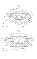
本発明の実施形態として、電子部品100の一例を説明する。図1(a)は第1例の電子部品100を表から見たときの平面模式図であり、図1(b)は第1例の電子部品100を裏から見たときの平面模式図である。図2(a)、(b)は第1例の電子部品100の断面模式図である。図2(a)は図1(a)、(b)のA−a線における第1例の電子部品100の断面図であり、図2(b)は図1(a)、(b)のB−b線における第1例の電子部品100の断面図である。図3(a)、(b)は第1例の電子部品100の変形例である、第2例の電子部品100の、図2(a)、(b)と同様の箇所の断面図である。以下、主に第1例の電子部品100について、同じもしくは類似の部分には共通の符号を付けて、各図面を相互に参照しながら説明を行う。各図にはX方向、Y方向、Z方向を示している。
As an embodiment of the present invention, an example of the
電子部品100は電子デバイス10と、電子デバイス10を収容する容器50を備える。容器50は、主に基体20と蓋体30と枠体40で構成される。詳しくは後述するが、容器50の内で基体20と枠体40は実装部材として機能し得る。蓋体30は光学部材として機能し得る。枠体40は電子デバイス10に対応する開口を有する。電子デバイス10は基体20に固定される。蓋体30は枠体40を介して基体20に固定され、内部空間60を介して電子デバイス10に対向する。枠体40は蓋体30と電子デバイス10との間の内部空間60を囲む。換言すれば、枠体40の開口内に上述した内部空間60が形成される。
The
電子部品100を構成する部材の位置関係は、電子デバイス10の位置に関連する基準面をもとに説明することができる。基準面は電子デバイス10の表面101と電子デバイス10の裏面102との間に位置し、電子デバイス10の側面105を貫く仮想的な平面である。表面101は基準面の一方の側(表面側)に位置し、裏面102は基準面の他方の側(裏面側)に位置する。基準面RPはX−Y方向に沿った平面であり、基準面RPに垂直な方向がZ方向である。面は電子デバイス10が半導体デバイスである場合、便宜的に、基準面RPを半導体層と絶縁体層との界面に設定してもよい。典型的には、X方向およびY方向は電子デバイス10の表面101、電子デバイス10の裏面102、蓋体30の外面301および蓋体30の内面302に平行な方向である。表面101は内面302に対向し、裏面102は基体20の配置領域210に対向して基体20に接着されている。また、Z方向はこれら表面101、裏面102、外面301、内面302に垂直な方向である。典型的な電子デバイス10および電子部品100はX方向およびY方向において矩形を呈する。また、Z方向における寸法はX方向、Y方向における寸法よりも小さく、おおむね平板形状である。以下、便宜的にZ方向における寸法を厚みもしくは高さと呼ぶ。ここで正射影領域について説明する。或る部材の正射影領域とは、基準面に垂直なZ方向においてその部材を投影可能な領域である。或る部材とは別の部材が、或る部材の正射影領域に位置することは、Z方向において、或る部材と別の部材とが重なることを意味する。つまり、或る部材の正射影領域内に別の部材が位置する場合、別の部材は、Z方向において或る部材と重なる領域に位置すると云うことができる。逆に、或る部材の正射影領域外に別の部材が位置する場合、別の部材の少なくとも一部は、或る部材と重らない領域に位置すると云うことができる。正射影領域の内外の境界は、対象の部材の輪郭である外縁および内縁(内縁は存在しない場合もある)に対応する。例えば、電子デバイス10に対向する蓋体30は、Z方向において電子デバイス10に重なる領域である、電子デバイス10の正射影領域に位置する。
The positional relationship of the members constituting the
X方向およびY方向において、電子部品100の外縁は、基体20の外縁205と枠体40の外縁405と蓋体30の外縁305で規定される。枠体40は外縁405に加えて内縁403を有する。枠体40の開口はこの内縁403により画定される。
In the X direction and the Y direction, the outer edge of the
電子デバイス10の種類は特に限定されないが、典型的には光デバイスである。本例の電子デバイス10は主部1と副部2を有している。典型的には主部1は電子デバイス10の中央に位置し、副部2はその周辺に位置する。電子デバイス10がCCDイメージセンサーやCMOSイメージセンサーなどの撮像デバイスであるなら主部1は撮像領域である。電子デバイス10が液晶ディスプレイやELディスプレイなどの表示デバイスであるなら主部1は表示領域である。撮像デバイスの場合、電子デバイス10の蓋体30との対向面である表面101が光入射面となる。この光入射面は、受光面を有する半導体基板の上に設けられた多層膜の最表層によって構成することができる。多層膜は、カラーフィルタ層やマイクロレンズ層、反射防止層、遮光層などの光学的な機能を有する層、平坦化層等の機械的な機能を有する層、パッシベーション層などの化学的な機能を有する層などを含む。副部2には主部1を駆動するための駆動回路や主部1からの信号(あるいは主部1への信号)を処理する信号処理回路が設けられる。電子デバイス10が半導体素子であると、このような回路をモノリシックに形成することが容易である。副部2には電子デバイス10と外部との信号の通信を行うための電極3(電極パッド)が設けられる。
The type of the
基体20の中央領域の少なくとも一部が配置領域210である。配置領域210の上には電子デバイス10が配置され、電子デバイス10は基体20に固定される。典型的には、電子デバイス10は、図2(a)、(b)に示す様に、基体20の配置領域210と電子デバイス10の裏面102との間に配された接合材52を介して固定される。ただし、接合材52が電子デバイス10の側面である外縁105のみに接していて、基体20の配置領域210と電子デバイス10の裏面102との間に接合材52が位置しない形態であってもよい。接合材52は導電性であってもよいし絶縁性であってもよい。また、接合材52は高い熱伝導性を有することが好ましく、金属粒子を含有するものを用いることもできる。
At least a part of the central region of the
基体20は、容器50の内側(内部空間60)に面する内部端子5と、容器50の外側に面する外部端子7とを有する。複数の内部端子5が並んで内部端子群を構成している。本例では、図1(a)に示すように、X方向に沿って列状に並んだ10個の内部端子5からなる内部端子群がY方向に2列分(2群)配されている。このような内部端子5の配置に限らず、Y方向に沿って列状に並んだ内部端子群をX方向に2列分配することもできる。また、Y方向に沿って列状に並んだ内部端子群とX方向に沿って列状に並んだ内部端子群とをそれぞれ2列分配して、電子デバイス10を内部端子5が囲むようにすることもできる。また、複数の外部端子7が並んで外部端子群を構成している。本例、図1(b)に示すように、ではX方向およびY方向に沿って行列状に並んだ外部端子群が電子部品100の裏側を成す、基体20の裏面206上に配されている。このような外部端子7の配置に限らず、外部端子群を、基体20の側面である外縁205に沿って、X方向および/またはY方向において、列状に設けることもできる。
The
内部端子5と外部端子7は基体20に内部配線として埋設された埋設部6を介して電気的に連続している。電子部品100を構成する電子デバイス10の電極3と容器50の内部端子5は、接続導体4を介して電気的に接続されている。本例では電極3と内部端子5の接続はワイヤーボンディング接続であって、接続導体4は金属ワイヤー(ボンディングワイヤー)であるが、電極3と内部端子5の接続をフリップチップ接続としてもよい。その場合、電極3は電子デバイス10の裏面102に設けられ、内部端子5や接続導体4は配置領域210に位置する。外部端子7は本例ではLGA(Land Grid Array)であるが、PGA(Pin Grid Array)やBGA(Ball Grid Array)、LCC(Leadless Chip Carrier)でもよい。このような形態では、複数の外部端子7は基体20上において蓋体30の正射影領域に位置し得る。外部端子7は基体20の正射影領域に位置することになる。さらに複数の外部端子7の一部は、基体20上において電子デバイス10の正射影領域に位置し得る。このように、外部端子7は、Z方向において電子デバイス10、基体20および蓋体30の少なくともいずれかに重なる領域に位置することができる。内部端子5と埋設部6と外部端子7とをリードフレームを用いて一体化してもよく、その場合、内部端子5がインナーリードとなり、外部端子7がアウターリードとなる。リードフレームを用いた形態では、複数の外部端子7は基体20の外縁205から突出して、基体20や蓋体30やの正射影領域の外に位置することになる。電子部品100は、その外部端子7がプリント配線板などの配線部材の接続端子と電気的に接続され、同時に、この配線部材に固着される。外部端子7は、はんだペーストを用いたリフローはんだ付けによって外部回路と電気的に接続することができる。このようにして電子部品100は配線部材に2次実装されて電子モジュールを構成する。電子モジュールもまた、電子部品として扱うことができる。実装の形態としては表面実装が好ましい。電子モジュールを筐体に組み込むことで、電子機器を構成する。
The
基体20は、中央領域が、中央領域を囲む周辺領域に対して窪んだ形状、すなわち凹形状を有している。具体的には、板状部により凹形状の中央領域である底部が、板状部の周辺領域の上に設けられた枠状部により凹形状の周辺領域である側部が構成される。基体20は、板材と枠材を積層することにより形成することができるほか、金型成形や切削加工等により一体的に形成することもできる。基体20は、内部端子5および外部端子7の絶縁を確保できれば金属板などの導電体でもよいが、典型的には絶縁体からなる。基体20は、ポリイミド基板などのフレキシブル基板であってもよいが、ガラスエポキシ基板、コンポジット基板、ガラスコンポジット基板、ベークライト基板、セラミック基板などのリジッド基板であることが好ましい。特にセラミック基板であることが好ましく、基体20のセラミック基板にはセラミック積層体を用いることが好ましい。セラミック材料としては炭化シリコン、窒化アルミニウム、サファイア、アルミナ、窒化シリコン、サーメット、イットリア、ムライト、フォルステライト、コージライト、ジルコニア、ステアタイト等を用いることが可能である。
The
図2(a)、図2(b)、図3(a)、図3(b)にそれぞれ示す様に、凹形状の基体20の周辺領域は、段部と段差部で構成されている。段部とはX方向、Y方向に広がる部分であり、段差部とは、Z方向における高さが互いに異なる二つの段部の間に位置し、Z方向に広がる部分である。
As shown in FIGS. 2 (a), 2 (b), 3 (a), and 3 (b), the peripheral region of the
ここで、内部端子5が設けられた段部を基準段部202と定める。本実施形態では、図2(a)、図3(a)に示す様に、Y方向において内部端子群よりも容器50の外縁側、つまり基体20の外縁205側に上段部204が位置している。そして上段部204は基準段部202に対して出張っている(突出している)。つまりZ方向において上段部204は基準段部202よりも蓋体30側に位置する。基準段部202と上段部204の間には段差部203が位置している。段差部203は接続導体4と内部空間60の一部を介して対向している。
Here, the step portion provided with the
また、図2(a)、(b)に示した例では、基体20が、基準段部202と上段部204に加えて、下段部200を有する。下段部200は、内部端子群よりも基体20の外縁205から離れて位置する。つまり、下段部200は内部端子群よりも基体20の内方に位置する。そして、下段部200は、段差部201を介して基準段部202に対して窪んでいる。つまり、下段部200はZ方向において段差部201を介して、内部端子群よりも蓋体30から離れて位置する。段差部201は電子デバイス10の外縁105と内部空間60の一部を介して対向している。基準段部202は上段部204と下段部202の間に位置している。したがって、基準段部202を中段部と呼ぶこともできる。図2(b)に示す様に、内部端子5が設けられていないX方向においては、下段部200と上段部204の間には基準段部202は設けられていない。そして段差部203が上段部204と下段部200の間に位置している。X方向においても、Y方向と同様に、上段部204と下段部200の間に中段部を設けることもできるが、このように内部端子5が設けられないような中段部は、容器50の不要な大型化を招くため、設けないことが好ましい。
In addition, in the example shown in FIGS. 2A and 2B, the
次に、電子部品100の変形例を図3(a)、(b)を用いて説明する。図3(a)、(b)は、図2(a)、(b)と同様の箇所の断面図である。図3(a)、(b)に示した変形例では、内部端子5が配される基準段部202に電子デバイス10が固定されており、図2(a)、(b)に示したような下段部200が無い。図2(a)の例では、基体20は3段構成であるのに対し、図3(a)の例では、基体20は2段構成である。基準段部202から段差部203を介して出張った上段部204を有する点は図3(a)と同様である。図3(a)、(b)における基体20は枠体40が接着された上段部と電子デバイス10が接着された下段部を有し、この下段部を内部端子5が設けられた基準段部202とみなすこともできる。
Next, a modified example of the
電子デバイス10に対向する蓋体30は、電子デバイス10を保護する機能を有する。電子デバイス10が光を扱うような撮像デバイスや表示デバイスであるならば、それらの光(典型的には可視光)に対して透明であることが求められる。そのような蓋体30としての好ましい材料はプラスチックやガラス、水晶などが挙げられる。蓋体30の表面には反射防止コーティングや赤外カットコーティングを設けることもできる。
The
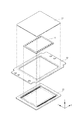
図4は電子部品100の分解図である。図4から理解されるように、電子部品100は、あらかじめ用意された電子デバイス10と基体20と蓋体30と枠体40とZ方向に重ね合わせて構成されている。図4では、基体20と枠体40との関係を長破線で、電子デバイス10と基体20との関係を一点鎖線で、枠体40と蓋体30との関係を二点鎖線で示している。また、蓋体30の輪郭を枠体40に、電子デバイス10の輪郭を基体20に、枠体40の輪郭を基体20にそれぞれ破線で示している。
FIG. 4 is an exploded view of the
蓋体30は枠体40を介して基体20に固定されている。詳細には、枠体40と基体20とが、図2(a)、(b)に示す様に、基体20の中央領域を囲む周辺領域で接合材51を介して相互に接着されている。また、枠体40と蓋体30とが、図2(a)、(b)に示す様に蓋体30の中央領域を囲む周辺領域で接合材53を介して相互に接着されている。基体20の中央領域と蓋体30の中央領域との間に電子デバイス10および内部空間60が位置している。本実施形態では、蓋体30は、Z方向において枠体40よりも電子デバイス10や基体20から離れて位置しており、蓋体30の電子デバイス10との対向面である内面302に接合材53が設けられている。しかし、特開2003−101042号公報の図3の形態の様に、枠体40の一部をZ方向において蓋体30よりも電子デバイス10や基体20から離れて位置させて、蓋体30の外面301に接合材53を設けることもできる。
The
具体的には、枠体40と基体20を接着剤を用いて相互に接着し、電子デバイス10と基体20を接着剤を用いて相互に接着し、蓋体30と枠体40を接着剤を用いて相互に接着する。これらの接着の順番は特に限定されないが、蓋体30と枠体40との接着に先立って枠体40と基体20との接着を行う場合に、本発明は好適である。また、電子デバイス10と基体20との接着に先立って枠体40と基体20との接着を行う場合に本発明は好適である。つまり、まず枠体40と基体20とを接着して実装部材を形成する。その実装部材に電子デバイス10を固定したのち、蓋体30を実装部材に接着するのである。
Specifically, the
基体20と枠体40は、接合材51によってそれらの接合面の全周で接合されることが好ましい。また、蓋体30と枠体40も接合材53によってそれらの接合面の全周で接合されることが好ましい。このように、基体20および蓋体30のそれぞれの周辺領域の全周を接着領域として、電子デバイス10の周囲の内部空間60を外部の空気に対して気密な空間とすることにより、内部空間60への異物の侵入が抑制され、信頼性が向上する。気密性を確保するためには、十分な量の接着剤を用いればよい。例えば、接合材51、52、53の厚みはそれぞれ1μm以上1000μm以下であり、典型的には10μm以上100μm以下である。
It is preferable that the
上で説明した接合材51、接合材52、接合材53は、それぞれ、塗布された接着剤が固化したものである。接着剤の種類としては、溶媒の蒸発による乾燥固化型、光や熱による分子の重合などによって硬化する化学反応型、融解した接着剤の凝固によって固化する熱溶融(ホットメルト)型などが挙げられる。典型的な接着剤としては、紫外線や可視光で硬化する光硬化型樹脂や、熱で硬化する熱硬化型樹脂が用いられる。接合材51用および接合材52用の接着剤としては熱硬化型樹脂を好適に用いることができ、接合材53用の接着剤としては光硬化型樹脂を好適に用いることができる。接着剤および接合材の色見としては、熱硬化性樹脂の場合には、白、黒、透明等特に限定は無く用いることが可能である。光硬化型樹脂の場合には、可視光及び/又は紫外光に対して透明である。接着剤および接合材は適度に無機あるいは有機のフィラーを含んでいてもよい。フィラーを含むことで耐湿性を向上することが可能である。接着剤の硬化後の接合材の弾性率は特に限定は無いが、異種材料同士を接着する場合には、比較的柔らかい樹脂(低弾性率樹脂)が好ましく、例えば1MPa以上100GPa以下の範囲が好適であるが、これに限るものではない。
The
枠体40は、基体20に対向し接合材51に接着された接合面401と、蓋体30に対向し接合材53に接着された接合面402を有する。枠体40は電子デバイス10と蓋体30の間の内部空間60を囲むように設けられている。枠体40の、内部空間60に面して内部空間60を囲む面が内縁403である。枠体40の外縁405は外部空間に露出している。本例の枠体40は、X方向において、基体20と蓋体30との間から外部空間に向かって延在した拡張部404を有している。この拡張部404には、貫通穴406が設けられており、この貫通穴406を、電子機器の筐体等に固定するためのねじ止め用の穴として用いたり、位置決め用の穴として用いたりすることができる。電子デバイス100が撮像デバイスである場合、電子機器としては、スチルカメラやビデオカメラ等の撮像装置や、撮影機能を有する情報端末が含まれる。
The
内部空間60の気密性を高める上では、枠体40は切れ目なく内部空間60を囲んでいることが好ましい。また、枠体40の剛性、ひいては電子部品100の剛性を確保する上でも、枠体40は切れ目のない閉ループであることが好ましい。また、後述するように熱伝導性を確保する上でも、枠体40は周方向において連続した閉ループであることが好ましい。しかしながら、製造上の制約により枠体40を辺ごとに複数に分割して配置してもよい。また、内部空間60と外部空間を連通させる目的で枠体40にスリットを設けてもよい。このように枠体40に切れ目が存在する場合、枠体40に生じる不連続な部分(スリット)は極力少ないことが望ましく、具体的には、内部空間60や電子デバイス10を囲む周の長さの10%未満にとどめておくことが望ましい。換言すれば、内部空間60や電子デバイス10を囲む周に沿って、その周の長さの90%以上にわたって枠体40が存在すれば、枠体40はこれらを囲むとみなすことができる。例えば、内縁403が縦20mm、横20mmの四辺形(内縁403の周長は80mm)であるとすれば、枠体40に設けるスリットの幅は総計で8mm未満であれば、枠体40が内部空間60を囲んでいるとみなすことができる。この場合でも、1つあたりのスリットの幅は小さいことが好ましく、例えば8mm幅のスリットを1つ設けるよりは、4mm幅のスリットを2つ設ける方がよい。
In order to increase the airtightness of the
枠体40の材料としては、樹脂、セラミック、金属を適宜使用することが可能である。なおここでいう金属とは単体の金属のみならず合金を含むものである。本実施形態は、接着剤を用いて枠体40と基体20とを貼り合せるものであるから、枠体40の材料が基体20の材料と異なる場合に好適である。また、本実施形態は、枠体40の材料が蓋体30の材料と異なる場合にも好適である。そのような場合とは、例えば、基体20の材料がセラミックであり、蓋体30の材料がガラスであり、枠体40の材料が金属または樹脂である場合である。
As a material of the
枠体40が高い熱伝導性を有する場合、拡張部404を介して電子デバイス10の熱を放熱することができる。放熱のためには、枠体40の熱伝導率は1.0W/m・K以上であることが好ましく、10W/m・K以上であることがより好ましい。典型的な樹脂の熱伝導率は1.0W/m・K未満である。
When the
また、電子部品100に生じる応力を緩和する上で、枠体40の熱膨張率(線膨張率)は極力低いことが好ましい。具体的には枠体40の熱膨張率は50ppm/K以下であることが好ましい。一般的な樹脂の熱膨張率は50ppm/Kより大きい。
Moreover, in order to relieve the stress generated in the
これら熱伝導や熱膨張の観点を考慮すると、枠体40の材料としては金属あるいはセラミックであることが好ましい。セラミックは金属と同等の熱的特性を有し得るが脆性材料であることから、加工性や機械的強度の点でセラミックよりも金属が好ましい。典型的な金属材料としては、アルミニウム、アルミニウム合金、銅、銅合金、鉄、鉄合金などが挙げられる。これら材料は加工性に優れ、比較的安価でもある。また、電子デバイス10が撮像デバイスである場合には、屋外での使用を考えると、耐食性に優れるアルミニウムやアルミニウム合金、鉄合金が好適である。さらに、枠体40の材料としては、ステンレスを始めとして、クロムやニッケル、コバルトを含む鉄合金が好適である。例えば、このような材料として、フェライト系ステンレスであるSUS430やオーステナイト系ステンレスであるSUS304、42アロイ、コバールなどを用いることができる。
Considering these viewpoints of heat conduction and thermal expansion, the
枠体40は、電子デバイス10と蓋体30との間隔を規定し、また、蓋体30を支持する機能をする。また、枠体40は、上述したようなねじ止め用や位置決め用の穴を有していたり、高い熱伝導性を有することにより放熱部材としての機能を有していたりする。そのため、基体20と枠体40とを併せて実装部材と呼ぶことができる。 電子部品100に関する製造方法の一例を説明する。図5〜7は図1(a)、(b)のA−a線における断面模式図である。
The
図5(a)は、基体20を用意する工程aを示す。上述したように基体20は、内部端子5と埋設部6と外部端子7を有している。また基体20は、基準段部202と上段部204とを接続する段差部203を有し、さらには、基準段部202と下段部200とを接続する段差部201を有している。内部端子5は基準段部202に設けられている。外部端子7は基体20の裏面206に設けられている。
FIG. 5A shows a process a for preparing the
このような基体20は、例えば以下のように形成されるセラミック積層体から構成される。まず、ドクターブレード法やカレンダーロール法等のシート成形法を用いて形成されたグリーンシートに板型の打ち抜き加工を施し、これを複数枚積層して生セラミックの板材を形成する。また、同様に形成されたグリーンシートに枠型の打ち抜き加工を施し、これを複数枚積層して生セラミックの枠材を形成する。これらの板材と枠材を重ねて焼成することで、凹形状を有するセラミック積層体を作製し、これを基体20として用いることができる。内部端子5、埋設部6および外部端子7は、グリーンシートを積層する過程でスクリーン印刷法等により形成された導電ペーストパターンを焼成することで形成することができる。
Such a base |
ここでは焼成前に、生セラミック板材であった第1層21と、小内径の生セラミック枠材であった第2層22および大内径の生セラミック枠材であった第3層23とを示している。第2層22の枠型と第3層23の枠型の内径を異ならせることにより、容易に基準段部202を形成可能である。なお、図3(a)、(b)に示したように、基体20を2段構成にするような場合には、図3(a)、(b)のような例では基体20を構成する枠材を2種類(2層)ではなく、1種類で構成することができる。そうすれば打ち抜き加工の枠型は1種類でよいので、コストダウンを図ることができる。基体20の段差部203の内径DBIや外径DBOは実装される電子デバイスのサイズに応じて任意に決定される。
Here, before firing, a
図5(b)は、基体20と枠体40を接着する工程のうちの前半の段階bを示す。成形された枠体40を用意する。枠体40の内径をDFI、外径をDFOとする。ここで、基体20と枠体40の大きさの関係を、DBI<DFIしておく。また、DBO<DFOとしておく。枠体40の表面には、サンドブラスト加工により凹凸をつけておくと良い。基体20の上段部204と枠体40の第1の接合面401の少なくとも一方に接着剤510を塗布する。図5(b)に示す様に、枠体40の接合面401のみに接着剤510を塗布すると良い。被塗物の塗布面にうねりがあると接着剤の塗布量がばらつくが、基体20よりも枠体40の方が平坦性が高く、接着剤510の塗布量を制御しやすいためである。上述したように、典型的な接着剤510は熱硬化型樹脂である。接着剤510の塗布には印刷法やディスペンス法等を用いることができる。
FIG. 5B shows the first stage b in the process of bonding the
図5(c)も、基体20と枠体40を接着する工程の内の後半の段階cを示す。枠体40を基体20の上段部204に乗せる。ここで、基体20の段差部203が、枠体40の内縁403よりも内部端子5側に位置している。このときの段差部203と内縁403のオフセット量DOSは、内径DFIと内径DBIの差に依存する。典型的にはDOS=(DFI−DBI)/2となる。当然、この時点で、接着剤510は液体である。枠体40の自重あるいは押圧により枠体40が基体20に押し付けられることにより、余分な接着剤510は枠体40と基体20の間からはみ出す場合がある。
FIG. 5C also shows the latter stage c in the process of bonding the
その後、塗布された接着剤510を適当な方法で固化させる。好適な接着剤510は熱硬化性樹脂であり、80〜200℃程度の加熱によって熱硬化させる。これにより、液体である接着剤510は固体である接合材51となり、接合材51を介して枠体40と基体20とが接着される。このようにして、枠体40と基体20を備える実装部材24を製造することができる。
Thereafter, the applied adhesive 510 is solidified by an appropriate method. A
図6(d)は、基体20に電子デバイス10を固定する工程dを示す。電子デバイス10は電極3を有している。基体20の下段部200と電子デバイス10の裏面102の少なくとも一方(典型的には基体20の下段部200のみ)にダイボンドペーストなどの接着剤520を塗布する。そして、電子デバイス10を接着剤520の上に配置する。この後、図6(e)で示す様に、接着剤520を固化して接合材52を形成して、電子デバイス10と基体20を接着する。
FIG. 6D shows a process d for fixing the
図6(e)は、電子デバイス10と基体20とを電気的に接続する工程eを示す。本例ではワイヤーボンディング接続を用いている。キャピラリ345の先端から供給される金属ワイヤーの一端を電極3に接続し、次いで、金属ワイヤーの他端を内部端子5に接続する。この金属ワイヤーにより接続導体4が形成される。なお、フリップチップ接続採用する場合には、バンプが接合材52と接続導体4とを兼ねることもできる。ここで、基体20は電子デバイス10を下段部200に設けて、内部端子5が設けられた基準段部202を下段部200より上方に位置させている構成である。そのため、キャピラリ345が段差部203、上段部204さらには電子デバイス10に干渉しうる範囲を小さくすることができる。そのため、電子部品100の小型化が可能となる。
FIG. 6E shows a step e of electrically connecting the
図6(f)は、蓋体30を枠体40に接着する工程の前半の段階fを示す。なお、図6(f)は、全ての内部端子5と全ての電極3とを接続導体4で接続した後の状態である。枠体40の接合面402と蓋体30の接合面(本例では内面302)の少なくとも一方に接着剤530を塗布する。上述したように、典型的な接着剤530は光硬化性樹脂である。接着剤530の塗布には印刷法やディスペンス法等を用いることができる。図6(f)に示す様に、蓋体30の内面302のみに接着剤530を塗布すると良い。ディスペンス法に依る場合、被塗物の塗布面にうねりがあると接着剤の塗布量がばらつくが、枠体40よりも蓋体30の方が平坦性が高く、接着剤530の塗布量を制御しやすいためである。
FIG. 6F shows the first stage f of the process of bonding the
図6(g)は、蓋体30を枠体40に接着する工程の後半の段階gを示す。蓋体30を枠体30の上に乗せる。当然、この時点で、接着剤530は液体である。そのため、蓋体30の自重あるいは押圧により蓋体30が枠体40に押し付けられることにより、余分な接着剤530は枠体40と蓋体30の間からはみ出す場合がある。
FIG. 6G shows the latter stage g of the process of bonding the
その後、塗布された接着剤530を適当な方法で固化させる。これにより、液体である接着剤530は固体である接合材53となり、接合材53を介して枠体40と蓋体30とが接着される。接着剤530として光硬化性樹脂を用いるのは以下の理由が挙げられる。接着剤530を接合面の全周に形成される場合、接着剤530として熱硬化性接着剤を用いると、加熱時に内部空間60が熱膨張して、内圧により液体状態の接着剤530を押し出してしまう可能性があるためである。光硬化性接着剤を用いるとこのような可能性はなくなる。なお、光硬化性接着剤を光硬化によって半硬化させた後であれば、後硬化として補助的に熱硬化を用いることができる。光硬化性の接着剤510を好適に用いるうえでは、蓋体30は紫外線などの接着剤510が反応する波長に対して十分な光透過性を有することが好ましい。以上の様にして、電子部品100を製造することができる。
Thereafter, the applied adhesive 530 is solidified by an appropriate method. Thereby, the
図7(h)は、電子モジュール600の製造方法の前半の段階hを示している。上記の様にして作製した電子部品100を2次実装するための配線部材500を用意する。配線部材は、リジッド配線板やフレキシブル配線板、リジッドフレキシブル配線板などであり、典型的にはプリント配線板である。配線部材500の接続端子9にはんだペースト80(はんだクリーム)をスクリーン印刷法などの公知の方法で塗布する。そして、電子部品100を基体20の裏面206を配線部材500側に向けて配線部材500の上に乗せて、接続端子9と外部端子7との間にはんだペースト80を介在させる。
FIG. 7H shows the first half h of the method for manufacturing the
図7(i)は、電子モジュール600の製造方法の後半の段階iを示している。電子部品100と配線部材500とを加熱炉(リフロー炉)の中に入れて、180〜250℃程度ではんだペースト80を熔融し、接続導体8としてのはんだを形成する。このようにして、電子部品100はリフローはんだ付けを経て配線部材500に固着される。このようにして、電子部品100と配線部材500とを備える電子モジュール600を製造することができる。なお配線部材500の上には電子部品100以外の電子部品、例えば集積回路部品やディスクリート部品等を搭載することができる。
FIG. 7 (i) shows the latter stage i of the method for manufacturing the
図7(j)は、電子機器1000を示している。電子モジュール600の配線部材500を外部回路700に接続する。外部回路は例えばプロセッサやメモリである。なお外部回路は、上述した修正機回路部品であってもよい。外部回路にはディスプレイ等の他の電子部品が接続される。これらを筐体900に格納して、電子機器1000を製造することが出来る。なお、電子部品100に設けられた放熱用の拡張部404は、筐体900や筐体900内に設けられたヒートシンクへ熱的に接続される。これにより、電子デバイス10で生じた熱が拡張部404を介して外部へ放熱される。
FIG. 7J shows the
本実施形態では、基体20と枠体40の関係が重要である。基体20と枠体40の関係はとりわけ基体20の形状に特徴づけられる。この関係を図2(a)あるいは図3(a)の上段部204の近傍の拡大である図8(a)を用いて、詳細を説明する。Y方向において、枠体40の内縁403は段差部203よりも内部端子群から離れて位置する。つまり、内縁403が段差部203から容器50の外縁側(外方)にオフセットしている。このオフセット量を、内縁403と段差部203とのY方向における距離DOSで示す。内縁403が段差部203からオフセットしているため、上段部204には、枠体40に対向する対向領域214と、枠体40に対向しない非対向領域224とが存在する。この非対向領域224は上段部204の段差部203側の領域であり、上段部204と段差部203との境界234から連続する領域である。境界234は、Y方向における上段部204の段差部203側の端であり、Z方向における段差部203の上段部204側の端である。このように、本実施形態の容器50においては、枠体40を用いて基体20の上段部204に非対向領域224を形成している。
In the present embodiment, the relationship between the
接合材51の、基体20と枠体40との間に位置する部分、詳細には、対向領域214と接合面401との間に位置する部分が、枠体40と基体20との接着に実質的に寄与する接合部511である。図8(a)に示す様に、典型的な接合材51は接合部511に加えて、はみ出し部512を有している。はみ出し部512は非対向領域224の上に位置している。
A portion of the
この非対向領域224により、接合材51が内部端子5や接続導体4、電子デバイス10に接触することを抑制できる。また、接合材53が内部端子5に接触することを抑制できる。オフセット量は、接合材51の、枠体40と基体20との間に位置して、実質的に接着に寄与する部分である接合部の厚みよりも大きくすると良い。接合材51の厚みは典型的には100μm未満であるから、オフセット量(距離DOS)は100μm以上であることが好ましい。さらに、オフセット量(距離DOS)は、段差部203の高さよりも大きいことが好ましい。接合の強さは接合材51の幅に依存するが、接合材51の幅を接合材51の厚みよりも大きくすることが好ましく、接合材51の幅を接合材51の厚みの10倍以上とすることが好ましい。例えば接合材51の幅は100μ以上10000μm以下であり、典型的には500μm以上5000μm以下である。
The
また、本実施形態では、Y方向において、枠体40の外縁405が、基体20の外縁205よりも内部空間60から離れて位置している。つまり、外縁405は外縁205に対して突出している。図8(c)は枠体40の外縁405の近傍の拡大である。接合材51は接合部511に加えてはみ出し部513を有することができる。枠体40の接合面401は基体20に対向する対向領域411に加え、非対向領域431を有している。本例では、枠体40の外縁405の全周が、基体20の外縁205よりも外側に位置している。つまり、拡張部404が設けられたX方向に限らず、Y方向においても、枠体40の外縁405は基体20の外縁205の対応する部分から突出している。そして、接合面401の非対向領域431の下には、接合材51のはみ出し部513が位置している。このはみ出し部513は外縁205に接していてもよいし、接していなくてもよい。
In the present embodiment, the
非対向領域224について説明する。上述したように、接着剤510を用いて枠体40と基体20を接着する際に、接着剤510のはみ出しが生じる。このはみ出しが、電子部品100の信頼性を低下させる場合がある。それは、はみ出した接着剤510が内部端子5に付着する場合である。
The
通常、内部端子5の接続導体4との接合面は、ニッケルなどの金属材料が露出している。そのため、接合面に樹脂が付着してしまうと、樹脂が水分を溜め易いことに起因して、金属材料が腐食しやすくなるという課題がある。また、当然ながら、接続導体4の接続前に内部端子5に絶縁性の接着剤510が付着していると、接続導体4と内部端子5との接続ができなくなったり、接続抵抗が高くなったりする。また、枠体40の接着前に、電子デバイス10の固定および接続導体4する場合であっても類似の問題が生じる。それは、接続導体4である金属ワイヤーと内部端子5の接続部近傍に付着した接着剤510に気泡が生じることである。気泡が製造時や使用時の温度変化で膨張/収縮することにより、金属ワイヤーや、その接続部にダメージを及ぼすためである。特に樹脂材料は水分を吸収しやすいため、気泡内に溜まった水分の蒸発および水蒸気の膨張/収縮の影響が大きい。
Usually, a metal material such as nickel is exposed on the joint surface of the
しかし、本実施形態では、上段部204には、枠体40と対向しない非対向領域224が設けられている。この非対向領域224上で、はみ出した接着剤510が保持される。しかし、形成された非対向領域224および境界234での表面張力により、はみ出した余分な接着剤510が保持され、内部端子5への接着剤510の付着が抑制される。図5(b)において説明したように、接着剤510を基体20に塗布することもできる。しかし、接着剤510を基体20に塗布すると、本来非対向領域224であるべき領域に、枠体40を配置する前から接着剤510が塗布されていたり、或いは、本来対向領域214であるべき領域に接着剤510が塗布されていなかったりする可能性が高くなる。そのような状況を避ける上でも、接着剤510を基体20ではなく枠体40に塗布するとよい。図8(a)は非対向領域224上で保持された状態で固化した接着剤510である接合材51の様子を示している。なお、図8(a)の例では接合材51が枠体40の内縁403に接しているが、内縁403の下端413で接着剤510が規制されて、接合材51が内縁403に接しない場合もある。
However, in the present embodiment, the
これに対し、オフセット量がゼロまたはマイナスの場合には、枠体40と基体20の間からはみ出した接着剤510が段差部203を伝って垂れてしまうことは容易に想像できよう。なお、オフセット量がマイナスの場合とは、段差部203が内縁403よりも外縁205側に位置している場合である。
On the other hand, when the offset amount is zero or minus, it can be easily imagined that the adhesive 510 protruding from between the
さらに、本実施形態では、はみ出た接着剤510のはみ出しは、上段部204と段差部203の境界234で止まりやすくなっている。これは、境界234での表面張力作用によるものと考えることができる。境界234における表面張力作用を高める上では、上段部204と段差部203が成す角度は、鋭角もしくは直角とすることが好ましい。基体20にセラミック積層体を用いると、この境界204の直角に近く、また曲率を大きくすることができる。上段部204と段差部203が鈍角を成す様に段差部203を斜面としても、同一面上にあるよりは、接合材51から内部端子5までの沿面距離を長くできるので一定の効果はある。しかし、境界234における表面張力作用は小さくなる。上段部204と段差部203が成す角度は、120°以上であることが好ましい。
Furthermore, in this embodiment, the protruding adhesive 510 is likely to stop at the
さらに、万が一、接着剤510が境界234を超えてはみ出したとしても、段差部203の高さ分に相当する量の接着剤は、段差部203で保持することができる。これに対して、段差部203を設けない場合には、段差部203の高さ分に相当する量のはみ出た接着剤を保持するためには、Y方向において段差部203の高さと同等の距離だけ、枠体40と基体20との接合面を内部端子5から外縁205側へ遠ざける必要がある。本実施形態では、Z方向に沿って延在する段差部203を設けていることから、Y方向における電子部品100の大型化を抑制することが可能となる。
Furthermore, even if the adhesive 510 protrudes beyond the
また、非対向領域224は蓋体30と枠体40との間に設けられた接着剤530がはみ出した場合にも有効である。図8(b)に示す様に、接着剤530が枠体40の内縁403を伝って垂れた場合でも、非対向領域224の直上あるいは非対向領域224上の接合材51の上で接着剤530を保持することができる。そのため、接着剤51と同様に、接着剤530が内部端子5や接続導体4に付着することを抑制することが出来る。接着剤53の液だれに対して、境界234や段差部203の存在による利点も接着剤51のそれと同様である。
The
図8(c)は、枠体40の外縁405近傍の拡大図である。枠体40に非対向領域431を設けることにより、はみ出し部513は表面張力作用よって非対向領域431に保持される。そのため、接着剤510が外縁205を伝って垂れることを抑制することができる。また、枠体40の外縁405を基体20の外縁205よりも大きくすることにより、次のような利点がある。例えば、検査のために電子部品100を平面視した際に、はみ出し部513が非対向領域431に隠れることで、はみ出し部513を電子部品100の外形と誤認することを避けることが出来る。また、電子部品100を運搬用の収納器に収納したした際に、運搬時に電子部品100が動いて電子部品100が収納器と擦れても、樹脂からなるはみ出し部513が収納器と擦れてパーティクルを生じることが避けられる。
FIG. 8C is an enlarged view of the vicinity of the
枠体40と蓋体30の間には、接合材53内にスペーサ530が設けられている。スペーサ530は典型的には球状の粒子であり、枠体40と蓋体30の間に位置して、枠体40と蓋体30の双方に接している。つまり、球状の粒子が枠体40と蓋体30の間に介在している。スペーサ530を設けることにより、接合材53の厚みと接着剤530のはみ出しを好適に制御することができる。なお、枠体40と基体20の間にもスペーサを配してもよい。
A
図8(d)は、図2(a)の、段差部201近傍の拡大図である。基体20に、基準段部202とは別の下段部200を設けて、下段部200に電子デバイス10を接着することにより、電子部品100の小型化が可能となる。図3(a)のように、基準段部202に電子デバイス10を接着する場合、配置領域210と電子デバイス10との間からはみ出た接合材52が内部端子5に接触することを避けるために、電子デバイス10と内部端子5を大きく離す必要がある。しかし、その点、図2(a)で説明した例では、図8(d)のように、Z方向において内部端子5を接着剤520から離している。このようにすると、はみ出た接合材52は段差部200で堰き止められる。そのため、Y方向における内部端子5と電子デバイス10との距離を大きくとらずとも、下段部200の上段に当たる基準段部202に位置する内部端子5に接合材52が接触することが抑制される。そのため、電子デバイス10の外縁105と内部端子5との距離を小さくして電子部品100の小型化を図っても、信頼性の低下が抑制される。むしろ、電極3と内部端子5との距離を小さくできるため、信頼性の向上が見込まれる。また、図8(d)に点線で示す様に、上段部204は、電子デバイス10の蓋体30との対向面である表面101よりも蓋体30から離れて位置していてもよい。これはつまり、電子デバイス10と蓋体30との距離が、上段部204と蓋体30との距離よりも大きくなる状態であり、上段部204が電子デバイス10を囲むことになる。この時、典型的には枠体40の接合面401が電子デバイス10を囲むように設けられる。一方、枠体40の接合面402は電子デバイス10の表面101よりも上方に位置し、最終的に接合面402は電子デバイス10を囲まず、内部空間60を囲む。このように、枠体40が内部空間60および電子デバイス10を囲むように設けることが好ましい。
FIG. 8D is an enlarged view of the vicinity of the
以下、本発明の実施例を説明する。図2に示した第1例の電子部品100と図3に示した第2例の電子部品100を作製した。比較例の電子部品100も作製した。いずれもX方向が長手方向でY方向が短手方向となる矩形板状の電子部品100である。
Examples of the present invention will be described below. The
第1例の電子部品100においては、形状が互いに異なるアルミナセラミックを3層積層した矩形凹状の基体20を準備した。基体20においては、板状である第1層21の厚みが0.8mm、枠状である第2層22の厚み(段差部201の高さ)が0.4mm、枠状である第3層23の厚み(段差部203の高さ)が0.2mmである。第1層21のX方向における外径は32.0mmである。第1層21のY方向における外径は26.4mmである。第2層22のX方向における外径は32.0mmで内径は26.2mm(枠幅が2.9mm)である。第2層22のY方向における外径は26.4mmで内径は19.6mm(枠幅は3.4mm)である。第3層23のX方向における外径は32.0mmで内径は26.2mm(枠幅が2.9mm)である。第3層23のY方向における外径(DBOに相当)は26.4mmで内径(DBIに相当)は21.4mm(枠幅が2.5mm)である。内部端子5が設けられた基準段部202のY方向における幅はそれぞれ0.9mmとしている。
In the
第2例の電子部品100においては、アルミナセラミックを2層積層した矩形凹状の基体20を準備した。基体20においては、板状である第1層21の厚みが0.8mm、枠状である第2層22の厚みが0.6mmである。第2層22のX方向、Y方向における外径、内径はそれぞれ、第1例の第3層23と同じである。
In the
比較用の電子部品100においては、アルミナセラミックの矩形平板状の基体20を準備した。基体20においては、板状である第1層21の厚みが0.8mmである。第1層21のX方向、Y方向における外径は第1例の第1層21と同じである。
In the
それぞれ、内部端子5、外部端子7として、ニッケルと金の積層膜を用いている。外部端子7はLGA型であり、125個の外部端子7が設けられている。
As the
次に、フェライト系ステンレスであるSUS430(18クロムステンレス)からなる枠体40を用意し、枠体40の一方の面に接着剤510として熱硬化型樹脂をスクリーン印刷で塗布した。そして、基体20の上段部204に載置した後加重した。熱硬化性樹脂の厚みが10〜50μmとなるように荷重を調整した。この時、接着剤510が枠体40と基体20の間からはみ出したことを確認した。そして、120〜150℃程度の加熱を行って接着剤510としての熱硬化性樹脂を硬化させた。尚、枠体40の表面は、熱硬化性樹脂との接着力を向上させる為に、表面粗さRa値0.1〜0.2μm程度のサンドブラスト処理を実施して、表面に凹凸形状を形成しておいた。枠体40の厚みは0.8mm、X方向における外径は42.0mm(うち、左右に設けた拡張部404の幅は各4.5mm)で内径は27.4mmである。枠体40のY方向における外径は27.4mmで内径は22.6mmである。この時、枠体40の内縁403と基体20の段差部203とのオフセット距離を、X方向の左右において各0.60mm、Y方向の上下において各0.60mmとした。内縁403を段差部203よりも大きくすることにより、内縁403の全周が段差部203の外方(外縁205側)に位置するようになっている。また、枠体40は基体20の外縁205に対して、X方向の左右において最小で0.50mm最大で5.0mm(拡張部404分)だけ突出しており、Y方向の上下において0.50mmだけ突出している。外縁405を外縁205よりも大きくすることにより、外縁405の全周が外縁205の外方(外縁205側)に位置するようになっている。
Next, a
次に、電子デバイス10として、いわゆるAPS−CサイズのCMOSイメージセンサーを準備した。この電子デバイス10を、黒色のダイボンディング接着剤である接着剤520を用いて、基体20のほぼ中央に熱硬化により固定した。その後、チップの周辺領域に設けられ電極3と内部端子5とを、ワイヤーボンディング装置を用いて、金ワイヤーにて電気的接続を行った。電子デバイス10の外縁105と枠体40の内縁403との距離は、X方向においては1.5mm、Y方向においては2.3mm(DCFに相当)である。そして、電子デバイス10と段差部203との距離はX方向においては0.9mm、Y方向においては1.7mmである。内部端子5と電子デバイス10の外縁105との距離DCTは第1例、第2例、比較例ともに0.8mmとした。
Next, a so-called APS-C size CMOS image sensor was prepared as the
次に、蓋体30として、α線対策された厚み0.5mmのガラス板を用意した。蓋体30のX方向における寸法は31.8mm、Y方向における寸法は26.3mmとし、基体20の外径寸法とほぼ一致させた。蓋体30の一方の面に接着剤530として紫外線硬化型樹脂をディスペンサで枠状に塗布し、接着剤530を塗布した面を枠体40の接合面402側にして、蓋体30を枠体40戴置し、適当に加重した。この時、接着剤530には直径30μmの球状粒子がスペーサ530として混入されており、接着剤530の厚みは概ね30μmとなった。この時、接着剤530が蓋体30と枠体40の間からはみ出したことを確認した。そして、蓋体30を介して紫外線を照射して光硬化処理を行った。さらに後硬化として、熱硬化処理を行って接着剤530を硬化させて、接合材53を形成した。電子デバイス10の表面101と蓋体30の内面302との距離は0.75mmとなった。このようにして、厚みが2.8mmの電子部品100を得た。
Next, a glass plate having a thickness of 0.5 mm, which is a measure against α rays, was prepared as the
第1例、第2例の電子部品100とも、接合材51と接合材52と接合材53のいずれの接合材の付着も確認できなかった。しかし、比較例の電子部品100では接合材51と接合材52と接合材53のいずれかが、内部端子5あるいは接続導体4に接触していることが確認された。また、上記目視検査に加えて、接続導体4としての金属ワイヤーに対して、接続強度を調べるためのプル強度検査も実施した。
Neither the
さらに第1例、第2例の電子部品100について、枠体40の内径DFIが上記したものと異なるものを用意して、DOSを0.1mm〜0.9mmの範囲で変化させた。その結果、目視検査およびプル強度検査ともに、良好な結果が得られた。このことは、例えばDOSを0.6mmから0.3mmにすることにより電子部品100の全体の寸法をさらに0.3mm縮小できることを意味している。
Further the first example, the
また、第1例、第2例の電子部品100について、電子デバイス10の外径が上記したものと異なるものを用意して、DCTを0.50mmとしたところ、第1例の電子部品100では目視検査およびプル強度検査でも良好な結果が得られたが、第2例の電子部品100ではプル強度検査において稀に不合格品が生じることが分かった。このことは第1例の電子部品100では電子部品の全体の寸法を第2例の電子部品100よりもさらに0.30mm縮小可能であることを意味している。
Further, the first example, the
5 内部端子
7 外部端子
10 電子デバイス
20 基体
200 下段部
201 段差部
202 基準段部
203 段差部
204 上段部
205 (基体の)外縁
210 配置領域
30 蓋体
40 枠体
403 (枠体の)内縁
404 拡張部
405 (枠体の)外縁
50 容器
51 接合材
52 接合材
53 接合材
60 内部空間
24 実装部材
100 電子部品
1000 電子機器
DESCRIPTION OF
Claims (20)
前記容器は、
前記電子デバイスが固定された基体と、
前記電子デバイスに対向する蓋体と、
前記蓋体と前記基体の間の空間を囲む枠体と、
を含み、
前記基体には、前記電子デバイスと電気的に接続された端子が配された基準段部と、前記基準段部よりも前記容器の外縁側に位置し、前記基準段部に対して段差部を介して出張った上段部と、が設けられており、
前記枠体は前記上段部に接着されおり、前記枠体の内縁が前記段差部よりも前記容器の前記外縁側に位置していることを特徴とする電子部品。 An electronic component comprising an electronic device and a container for housing the electronic device,
The container is
A substrate on which the electronic device is fixed;
A lid facing the electronic device;
A frame surrounding the space between the lid and the base;
Including
The base is provided with a reference step provided with a terminal electrically connected to the electronic device, and is positioned on the outer edge side of the container with respect to the reference step, and a step is provided with respect to the reference step. And an upper stage part that made a business trip through
The frame is bonded to the upper step, and the inner edge of the frame is located closer to the outer edge of the container than the step.
前記電子デバイスが固定される基体と、
前記基体に接着された枠体と、
を備え、
前記基体には、前記電子デバイスと電気的に接続される端子が配された基準段部と、前記基準段部よりも前記実装部材の外縁側に位置し、前記基準段部に対して段差部を介して出張った上段部と、が設けられており、
前記枠体は前記上段部に接着され、前記枠体の内縁が前記段差部よりも前記実装部材の前記外縁側に位置していることを特徴とする実装部材。 A mounting member for an electronic device,
A base to which the electronic device is fixed;
A frame bonded to the substrate;
With
The base is provided with a reference step portion on which a terminal electrically connected to the electronic device is disposed, and is located on the outer edge side of the mounting member with respect to the reference step portion, and a step portion with respect to the reference step portion And the upper stage part that made a business trip through
The frame member is bonded to the upper step portion, and the inner edge of the frame member is located closer to the outer edge side of the mounting member than the step portion.
電子デバイスが配置される基体と、枠体とを用意する工程と、
前記基体と前記枠体とを接着剤を用いて接着する工程と、
を有し、
前記基体には、前記電子デバイスと電気的に接続される端子が配された基準段部と、前記基準段部よりも前記基体の外縁側に位置し、前記基準段部に対して段差部を介して出張った上段部と、が設けられており、
前記接着する工程において、前記枠体の内縁が、前記段差部よりも前記基体の前記外縁側に位置するように、前記枠体を前記上段部に接着することを特徴とする実装部材の製造方法。 A method for manufacturing an electronic device mounting member, comprising:
Preparing a substrate on which an electronic device is arranged and a frame;
Bonding the base and the frame using an adhesive;
Have
The base is provided with a reference step portion on which a terminal electrically connected to the electronic device is disposed, and is positioned on the outer edge side of the base with respect to the reference step portion, and a step portion is provided with respect to the reference step portion. And an upper stage part that made a business trip through
In the bonding step, the frame body is bonded to the upper stage portion so that the inner edge of the frame body is located on the outer edge side of the base with respect to the stepped portion. .
請求項16または17に記載の実装部材の製造方法に実装部材に前記枠体の内縁の内側を介して電子デバイスを実装する工程と、
蓋体と前記枠体とを接着剤を用いて接着する工程と、
を有し、
前記基体には、前記電子デバイスと電気的に接続される端子が配された基準段部と、前記基準段部よりも前記実装部材の外縁側に位置し、前記基準段部に対して段差部を介して出張った上段部と、が設けられており、
前記接着する工程において、前記枠体の内縁が、前記段差部よりも前記基体の前記外縁側に位置していることを特徴とする電子部品の製造方法。 An electronic component manufacturing method comprising an electronic device and a lid facing the electronic device,
Mounting the electronic device on the mounting member via the inside of the inner edge of the frame in the mounting member manufacturing method according to claim 16 or 17,
Bonding the lid and the frame using an adhesive;
Have
The base is provided with a reference step portion on which a terminal electrically connected to the electronic device is disposed, and is located on the outer edge side of the mounting member with respect to the reference step portion, and a step portion with respect to the reference step portion And the upper stage part that made a business trip through
In the bonding step, the inner edge of the frame body is located closer to the outer edge side of the base than the stepped portion.
Priority Applications (3)
| Application Number | Priority Date | Filing Date | Title |
|---|---|---|---|
| JP2013039450A JP2013243340A (en) | 2012-04-27 | 2013-02-28 | Electronic component, mounting member, electronic apparatus, and manufacturing method of these |
| US13/869,852 US9155212B2 (en) | 2012-04-27 | 2013-04-24 | Electronic component, mounting member, electronic apparatus, and their manufacturing methods |
| CN201310150932.XA CN103378118B (en) | 2012-04-27 | 2013-04-27 | Electronic devices and components, installing component, electronic installation and their manufacture method |
Applications Claiming Priority (3)
| Application Number | Priority Date | Filing Date | Title |
|---|---|---|---|
| JP2012103829 | 2012-04-27 | ||
| JP2012103829 | 2012-04-27 | ||
| JP2013039450A JP2013243340A (en) | 2012-04-27 | 2013-02-28 | Electronic component, mounting member, electronic apparatus, and manufacturing method of these |
Publications (2)
| Publication Number | Publication Date |
|---|---|
| JP2013243340A true JP2013243340A (en) | 2013-12-05 |
| JP2013243340A5 JP2013243340A5 (en) | 2016-04-14 |
Family
ID=49462994
Family Applications (1)
| Application Number | Title | Priority Date | Filing Date |
|---|---|---|---|
| JP2013039450A Pending JP2013243340A (en) | 2012-04-27 | 2013-02-28 | Electronic component, mounting member, electronic apparatus, and manufacturing method of these |
Country Status (3)
| Country | Link |
|---|---|
| US (1) | US9155212B2 (en) |
| JP (1) | JP2013243340A (en) |
| CN (1) | CN103378118B (en) |
Cited By (3)
| Publication number | Priority date | Publication date | Assignee | Title |
|---|---|---|---|---|
| JP2015050557A (en) * | 2013-08-30 | 2015-03-16 | 京セラ株式会社 | Substrate for mounting image sensor and imaging apparatus |
| JP2015119091A (en) * | 2013-12-19 | 2015-06-25 | 京セラ株式会社 | Imaging element mounting board and imaging apparatus |
| KR20160000328A (en) * | 2014-06-24 | 2016-01-04 | 삼성전기주식회사 | Image sensor module and camera module including the same |
Families Citing this family (14)
| Publication number | Priority date | Publication date | Assignee | Title |
|---|---|---|---|---|
| JP2015038920A (en) * | 2013-08-19 | 2015-02-26 | ソニー株式会社 | Imaging apparatus and electronic apparatus |
| JP6214337B2 (en) * | 2013-10-25 | 2017-10-18 | キヤノン株式会社 | Electronic parts, electronic devices, and methods for manufacturing electronic parts. |
| KR20150101571A (en) * | 2014-02-27 | 2015-09-04 | 천병태 | Image sensor chip package |
| DE102016102327B4 (en) * | 2016-02-10 | 2018-02-08 | Schott Ag | Housing for an electronic component and laser module |
| JP2018157074A (en) * | 2017-03-17 | 2018-10-04 | キヤノン株式会社 | Electronic component, manufacturing method of the same, and electronic device |
| EP3505216B1 (en) * | 2018-01-02 | 2020-07-22 | Heraeus Deutschland GmbH & Co. KG | Electrical contacting device for an implantable medical device and method for producing |
| US20190373142A1 (en) * | 2018-05-31 | 2019-12-05 | Sharp Kabushiki Kaisha | Imaging apparatus |
| JP7134763B2 (en) | 2018-07-23 | 2022-09-12 | キヤノン株式会社 | Module and its manufacturing method |
| JP2020108004A (en) * | 2018-12-27 | 2020-07-09 | パナソニックIpマネジメント株式会社 | Electronic device heat dissipation structure and heat dissipation method |
| JP2020150207A (en) * | 2019-03-15 | 2020-09-17 | キヤノン株式会社 | Electronic component, manufacturing method of them, and equipment |
| CN111863843B (en) * | 2019-04-30 | 2024-03-01 | 同欣电子工业股份有限公司 | Sensor packaging structure and sensing module thereof |
| US10832993B1 (en) * | 2019-05-09 | 2020-11-10 | Texas Instruments Incorporated | Packaged multichip device with stacked die having a metal die attach |
| JP7406314B2 (en) * | 2019-06-24 | 2023-12-27 | キヤノン株式会社 | electronic modules and equipment |
| CN114685096B (en) * | 2020-12-25 | 2023-07-11 | 比亚迪股份有限公司 | Composite material and preparation method and application thereof |
Citations (17)
| Publication number | Priority date | Publication date | Assignee | Title |
|---|---|---|---|---|
| JPS63116461A (en) * | 1986-11-05 | 1988-05-20 | Tomoegawa Paper Co Ltd | Hermetic sealing for solid-state image pickup device |
| JPH04171746A (en) * | 1990-11-02 | 1992-06-18 | Fujitsu Ltd | Semiconductor device, and manufacture thereof |
| JPH05343548A (en) * | 1992-06-08 | 1993-12-24 | Ngk Spark Plug Co Ltd | Seal ring and manufacture thereof |
| JPH0653454A (en) * | 1992-07-29 | 1994-02-25 | Nec Kyushu Ltd | Glass cap sealing structure for image sensor |
| JPH09284617A (en) * | 1995-05-31 | 1997-10-31 | Sony Corp | Image pickup device and its production, image pickup adapter device, device and method for processing signal and device and method for processing information |
| JPH11112854A (en) * | 1997-10-07 | 1999-04-23 | Matsushita Electron Corp | Image pickup device |
| JP2000323593A (en) * | 1999-05-06 | 2000-11-24 | Yazaki Corp | Semiconductor device |
| JP2001068575A (en) * | 1999-08-27 | 2001-03-16 | Shinko Electric Ind Co Ltd | Seal ring for semiconductor device and manufacture of the semiconductor device |
| JP2004146392A (en) * | 2002-08-30 | 2004-05-20 | Kyocera Corp | Package for housing semiconductor element and semiconductor device |
| JP2004297282A (en) * | 2003-03-26 | 2004-10-21 | Mitsubishi Electric Corp | Camera module |
| JP2005203669A (en) * | 2004-01-19 | 2005-07-28 | Kyocera Corp | Package for housing electronic component, and electronic device |
| JP2005209790A (en) * | 2004-01-21 | 2005-08-04 | Fujikura Ltd | Electronic device package |
| JP2005352191A (en) * | 2004-06-10 | 2005-12-22 | Sony Corp | Imaging apparatus |
| JP2007266171A (en) * | 2006-03-28 | 2007-10-11 | Kyocera Corp | Ceramic container |
| JP2008235531A (en) * | 2007-03-20 | 2008-10-02 | Mitsubishi Electric Corp | Package for hermetic sealing, and connection structure |
| JP2008245244A (en) * | 2007-02-26 | 2008-10-09 | Sony Corp | Imaging element package, imaging element module, lens barrel, and imaging device |
| JP2011165775A (en) * | 2010-02-05 | 2011-08-25 | Canon Inc | Solid-state imaging device and method of manufacturing the same |
Family Cites Families (60)
| Publication number | Priority date | Publication date | Assignee | Title |
|---|---|---|---|---|
| US3622419A (en) * | 1969-10-08 | 1971-11-23 | Motorola Inc | Method of packaging an optoelectrical device |
| GB2007911B (en) | 1977-10-12 | 1982-03-24 | Secr Defence | Methods of packaging microwave intergrated circuits and to microwave intergrated circiuted packages |
| US4445274A (en) * | 1977-12-23 | 1984-05-01 | Ngk Insulators, Ltd. | Method of manufacturing a ceramic structural body |
| JPS62217640A (en) | 1986-03-19 | 1987-09-25 | Hitachi Ltd | Manufacture of solid state image sensing device |
| JPH0728014B2 (en) | 1986-05-21 | 1995-03-29 | 株式会社東芝 | Solid-state imaging device |
| JPH02291153A (en) | 1989-04-28 | 1990-11-30 | Mitsubishi Electric Corp | Semiconductor device |
| JPH04123462A (en) | 1990-09-14 | 1992-04-23 | Toshiba Corp | Semiconductor mounting device |
| KR940002444B1 (en) * | 1990-11-13 | 1994-03-24 | 금성일렉트론 주식회사 | Method of assembling package of semiconductor device |
| US5195023A (en) * | 1991-12-23 | 1993-03-16 | At&T Bell Laboratories | Integrated circuit package with strain relief grooves |
| US5481136A (en) * | 1992-10-28 | 1996-01-02 | Sumitomo Electric Industries, Ltd. | Semiconductor element-mounting composite heat-sink base |
| US5458716A (en) * | 1994-05-25 | 1995-10-17 | Texas Instruments Incorporated | Methods for manufacturing a thermally enhanced molded cavity package having a parallel lid |
| MY112145A (en) | 1994-07-11 | 2001-04-30 | Ibm | Direct attachment of heat sink attached directly to flip chip using flexible epoxy |
| JP3493844B2 (en) * | 1994-11-15 | 2004-02-03 | 住友電気工業株式会社 | Semiconductor substrate material, method of manufacturing the same, and semiconductor device using the substrate |
| JPH09172554A (en) | 1995-12-21 | 1997-06-30 | Dainippon Printing Co Ltd | Color look up table |
| JPH09266268A (en) | 1996-03-28 | 1997-10-07 | Mitsubishi Electric Corp | Semiconductor device manufacturing method and package of semiconductor device |
| US6011294A (en) * | 1996-04-08 | 2000-01-04 | Eastman Kodak Company | Low cost CCD packaging |
| US5879786A (en) * | 1996-11-08 | 1999-03-09 | W. L. Gore & Associates, Inc. | Constraining ring for use in electronic packaging |
| JP3129275B2 (en) | 1998-02-27 | 2001-01-29 | 日本電気株式会社 | Semiconductor device |
| JPH11354587A (en) * | 1998-06-08 | 1999-12-24 | Toyo Commun Equip Co Ltd | Method for mounting oscillator in flip-chip bonding |
| JP3690171B2 (en) | 1999-03-16 | 2005-08-31 | 株式会社日立製作所 | Composite material and its production method and application |
| JP2001168443A (en) | 1999-12-06 | 2001-06-22 | Kyocera Corp | Package for housing optical semiconductor element |
| JP2001308442A (en) | 2000-04-27 | 2001-11-02 | Kyocera Corp | Package for housing optical semiconductor element |
| JP2002026187A (en) | 2000-07-07 | 2002-01-25 | Sony Corp | Semiconductor package and manufacturing method therefor |
| US6979595B1 (en) * | 2000-08-24 | 2005-12-27 | Micron Technology, Inc. | Packaged microelectronic devices with pressure release elements and methods for manufacturing and using such packaged microelectronic devices |
| JP2002299486A (en) | 2001-03-29 | 2002-10-11 | Kyocera Corp | Package for storing optical semiconductor element |
| JP2003101042A (en) | 2001-09-25 | 2003-04-04 | Kyocera Corp | Container for accommodating optical semiconductor element |
| JP2003258141A (en) | 2002-02-27 | 2003-09-12 | Nec Compound Semiconductor Devices Ltd | Electronic component and its manufacturing method |
| JP3888228B2 (en) | 2002-05-17 | 2007-02-28 | 株式会社デンソー | Sensor device |
| DE10223035A1 (en) * | 2002-05-22 | 2003-12-04 | Infineon Technologies Ag | Electronic component with cavity housing, in particular high-frequency power module |
| JP2004003886A (en) * | 2002-05-31 | 2004-01-08 | Matsushita Electric Works Ltd | Sensor package |
| US7183485B2 (en) * | 2003-03-11 | 2007-02-27 | Micron Technology, Inc. | Microelectronic component assemblies having lead frames adapted to reduce package bow |
| US6953891B2 (en) * | 2003-09-16 | 2005-10-11 | Micron Technology, Inc. | Moisture-resistant electronic device package and methods of assembly |
| KR100609012B1 (en) | 2004-02-11 | 2006-08-03 | 삼성전자주식회사 | Wiring substrate and solid-state imaging apparatus using thereof |
| JP4686134B2 (en) | 2004-04-26 | 2011-05-18 | パナソニック株式会社 | Optical device and manufacturing method thereof |
| JP4473674B2 (en) * | 2004-08-06 | 2010-06-02 | パナソニック株式会社 | Semiconductor package and manufacturing method thereof |
| JP2006245090A (en) | 2005-03-01 | 2006-09-14 | Konica Minolta Holdings Inc | Package for semiconductor and manufacturing method thereof |
| JP4455509B2 (en) * | 2006-01-31 | 2010-04-21 | シャープ株式会社 | Semiconductor device |
| JP2007208045A (en) | 2006-02-02 | 2007-08-16 | Sony Corp | Imaging device, camera module, and method for manufacturing electronic equipment and imaging device |
| JP2007242908A (en) | 2006-03-09 | 2007-09-20 | Sumitomo Metal Electronics Devices Inc | Ceramic package for housing electronic components |
| JP2008118585A (en) * | 2006-11-08 | 2008-05-22 | Nippon Dempa Kogyo Co Ltd | Electronic component for surface mounting |
| JP2008147243A (en) * | 2006-12-06 | 2008-06-26 | Olympus Corp | Hermetic sealing apparatus |
| JP5115258B2 (en) * | 2008-03-17 | 2013-01-09 | セイコーエプソン株式会社 | Piezoelectric devices and electronic equipment |
| US20100315938A1 (en) * | 2008-08-14 | 2010-12-16 | Nanochip, Inc. | Low distortion package for a mems device including memory |
| US8058720B2 (en) * | 2008-11-19 | 2011-11-15 | Mediatek Inc. | Semiconductor package |
| JP5315028B2 (en) * | 2008-12-04 | 2013-10-16 | ルネサスエレクトロニクス株式会社 | Electronic device and method for manufacturing electronic device |
| JP5454134B2 (en) | 2008-12-27 | 2014-03-26 | セイコーエプソン株式会社 | Vibrating piece, vibrator, sensor and electronic component |
| JP2010238821A (en) | 2009-03-30 | 2010-10-21 | Sony Corp | Multilayer wiring substrate, stack structure sensor package, and method of manufacturing the same |
| JP2011077080A (en) | 2009-09-29 | 2011-04-14 | Panasonic Corp | Solid-state imaging device |
| JP5757573B2 (en) | 2009-10-08 | 2015-07-29 | 日本電気株式会社 | Semiconductor device |
| JP2011165745A (en) | 2010-02-05 | 2011-08-25 | Mitsubishi Electric Corp | Ceramic package |
| DE102011018296B4 (en) * | 2010-08-25 | 2020-07-30 | Snaptrack, Inc. | Component and method for producing a component |
| JP5399525B2 (en) * | 2011-06-29 | 2014-01-29 | シャープ株式会社 | Optical distance measuring device and electronic device |
| JP5588419B2 (en) * | 2011-10-26 | 2014-09-10 | 株式会社東芝 | package |
| WO2013118501A1 (en) | 2012-02-07 | 2013-08-15 | 株式会社ニコン | Imaging unit and imaging apparatus |
| US9653656B2 (en) * | 2012-03-16 | 2017-05-16 | Advanced Semiconductor Engineering, Inc. | LED packages and related methods |
| JP6192312B2 (en) * | 2013-02-28 | 2017-09-06 | キヤノン株式会社 | A mounting member manufacturing method and an electronic component manufacturing method. |
| JP5904957B2 (en) * | 2013-02-28 | 2016-04-20 | キヤノン株式会社 | Electronic components and electronic equipment. |
| JP5851439B2 (en) * | 2013-03-07 | 2016-02-03 | 株式会社東芝 | High frequency semiconductor package |
| US9668352B2 (en) * | 2013-03-15 | 2017-05-30 | Sumitomo Electric Printed Circuits, Inc. | Method of embedding a pre-assembled unit including a device into a flexible printed circuit and corresponding assembly |
| JP2014207313A (en) * | 2013-04-12 | 2014-10-30 | セイコーエプソン株式会社 | Electronic component, electronic apparatus and mobile |
-
2013
- 2013-02-28 JP JP2013039450A patent/JP2013243340A/en active Pending
- 2013-04-24 US US13/869,852 patent/US9155212B2/en not_active Expired - Fee Related
- 2013-04-27 CN CN201310150932.XA patent/CN103378118B/en not_active Expired - Fee Related
Patent Citations (17)
| Publication number | Priority date | Publication date | Assignee | Title |
|---|---|---|---|---|
| JPS63116461A (en) * | 1986-11-05 | 1988-05-20 | Tomoegawa Paper Co Ltd | Hermetic sealing for solid-state image pickup device |
| JPH04171746A (en) * | 1990-11-02 | 1992-06-18 | Fujitsu Ltd | Semiconductor device, and manufacture thereof |
| JPH05343548A (en) * | 1992-06-08 | 1993-12-24 | Ngk Spark Plug Co Ltd | Seal ring and manufacture thereof |
| JPH0653454A (en) * | 1992-07-29 | 1994-02-25 | Nec Kyushu Ltd | Glass cap sealing structure for image sensor |
| JPH09284617A (en) * | 1995-05-31 | 1997-10-31 | Sony Corp | Image pickup device and its production, image pickup adapter device, device and method for processing signal and device and method for processing information |
| JPH11112854A (en) * | 1997-10-07 | 1999-04-23 | Matsushita Electron Corp | Image pickup device |
| JP2000323593A (en) * | 1999-05-06 | 2000-11-24 | Yazaki Corp | Semiconductor device |
| JP2001068575A (en) * | 1999-08-27 | 2001-03-16 | Shinko Electric Ind Co Ltd | Seal ring for semiconductor device and manufacture of the semiconductor device |
| JP2004146392A (en) * | 2002-08-30 | 2004-05-20 | Kyocera Corp | Package for housing semiconductor element and semiconductor device |
| JP2004297282A (en) * | 2003-03-26 | 2004-10-21 | Mitsubishi Electric Corp | Camera module |
| JP2005203669A (en) * | 2004-01-19 | 2005-07-28 | Kyocera Corp | Package for housing electronic component, and electronic device |
| JP2005209790A (en) * | 2004-01-21 | 2005-08-04 | Fujikura Ltd | Electronic device package |
| JP2005352191A (en) * | 2004-06-10 | 2005-12-22 | Sony Corp | Imaging apparatus |
| JP2007266171A (en) * | 2006-03-28 | 2007-10-11 | Kyocera Corp | Ceramic container |
| JP2008245244A (en) * | 2007-02-26 | 2008-10-09 | Sony Corp | Imaging element package, imaging element module, lens barrel, and imaging device |
| JP2008235531A (en) * | 2007-03-20 | 2008-10-02 | Mitsubishi Electric Corp | Package for hermetic sealing, and connection structure |
| JP2011165775A (en) * | 2010-02-05 | 2011-08-25 | Canon Inc | Solid-state imaging device and method of manufacturing the same |
Cited By (4)
| Publication number | Priority date | Publication date | Assignee | Title |
|---|---|---|---|---|
| JP2015050557A (en) * | 2013-08-30 | 2015-03-16 | 京セラ株式会社 | Substrate for mounting image sensor and imaging apparatus |
| JP2015119091A (en) * | 2013-12-19 | 2015-06-25 | 京セラ株式会社 | Imaging element mounting board and imaging apparatus |
| KR20160000328A (en) * | 2014-06-24 | 2016-01-04 | 삼성전기주식회사 | Image sensor module and camera module including the same |
| KR101627135B1 (en) | 2014-06-24 | 2016-06-03 | 삼성전기주식회사 | Image sensor module and camera module including the same |
Also Published As
| Publication number | Publication date |
|---|---|
| CN103378118A (en) | 2013-10-30 |
| US20130286566A1 (en) | 2013-10-31 |
| US9155212B2 (en) | 2015-10-06 |
| CN103378118B (en) | 2016-03-16 |
Similar Documents
| Publication | Publication Date | Title |
|---|---|---|
| JP5885690B2 (en) | Electronic components and equipment | |
| JP2013243340A (en) | Electronic component, mounting member, electronic apparatus, and manufacturing method of these | |
| JP6296687B2 (en) | Electronic components, electronic modules, and methods for manufacturing them. | |
| JP6214337B2 (en) | Electronic parts, electronic devices, and methods for manufacturing electronic parts. | |
| US9225882B2 (en) | Electronic component packaging that can suppress noise and electronic apparatus | |
| JP6732932B2 (en) | Base for mounting image pickup element, image pickup device, and image pickup module | |
| KR101814546B1 (en) | Substrate for mounting electronic element, and electronic device | |
| US8928803B2 (en) | Solid state apparatus | |
| US9576877B2 (en) | Electronic component, electronic device, method of manufacturing mounted member, and method of manufacturing electronic component | |
| JP7059237B2 (en) | Electronic components, electronic modules and their manufacturing methods | |
| TW201246618A (en) | Led module device, method for manufacturing same, led package used for led module device, and method for manufacturing same | |
| TW201408149A (en) | Circuit board assembly and camera module | |
| JP2018010890A (en) | Electronic-element mounting substrate, electronic device, and electronic module | |
| JP6908506B2 (en) | Imaging device | |
| JP2007234683A (en) | Semiconductor device, and its manufacturing method | |
| JP2017195497A (en) | Imaging element mounting substrate, imaging device, and imaging module | |
| TW200910940A (en) | Image sensor | |
| JP2005303735A (en) | Imaging apparatus |
Legal Events
| Date | Code | Title | Description |
|---|---|---|---|
| A521 | Request for written amendment filed |
Free format text: JAPANESE INTERMEDIATE CODE: A523 Effective date: 20160226 |
|
| A621 | Written request for application examination |
Free format text: JAPANESE INTERMEDIATE CODE: A621 Effective date: 20160226 |
|
| A977 | Report on retrieval |
Free format text: JAPANESE INTERMEDIATE CODE: A971007 Effective date: 20170120 |
|
| A131 | Notification of reasons for refusal |
Free format text: JAPANESE INTERMEDIATE CODE: A131 Effective date: 20170131 |
|
| A521 | Request for written amendment filed |
Free format text: JAPANESE INTERMEDIATE CODE: A523 Effective date: 20170328 |
|
| A131 | Notification of reasons for refusal |
Free format text: JAPANESE INTERMEDIATE CODE: A131 Effective date: 20170711 |
|
| A521 | Request for written amendment filed |
Free format text: JAPANESE INTERMEDIATE CODE: A523 Effective date: 20170908 |
|
| A02 | Decision of refusal |
Free format text: JAPANESE INTERMEDIATE CODE: A02 Effective date: 20180123 |