JP2013088757A - 反射防止構造体 - Google Patents
反射防止構造体 Download PDFInfo
- Publication number
- JP2013088757A JP2013088757A JP2011231645A JP2011231645A JP2013088757A JP 2013088757 A JP2013088757 A JP 2013088757A JP 2011231645 A JP2011231645 A JP 2011231645A JP 2011231645 A JP2011231645 A JP 2011231645A JP 2013088757 A JP2013088757 A JP 2013088757A
- Authority
- JP
- Japan
- Prior art keywords
- light incident
- columnar
- wavelength
- refractive index
- antireflection
- Prior art date
- Legal status (The legal status is an assumption and is not a legal conclusion. Google has not performed a legal analysis and makes no representation as to the accuracy of the status listed.)
- Withdrawn
Links
- 239000010409 thin film Substances 0.000 abstract description 33
- 239000010408 film Substances 0.000 abstract description 27
- 230000002093 peripheral effect Effects 0.000 abstract 1
- 239000000758 substrate Substances 0.000 description 42
- 239000004065 semiconductor Substances 0.000 description 41
- 230000000694 effects Effects 0.000 description 28
- 230000003287 optical effect Effects 0.000 description 25
- 238000009826 distribution Methods 0.000 description 13
- 238000004519 manufacturing process Methods 0.000 description 13
- XUIMIQQOPSSXEZ-UHFFFAOYSA-N Silicon Chemical compound [Si] XUIMIQQOPSSXEZ-UHFFFAOYSA-N 0.000 description 12
- 238000006243 chemical reaction Methods 0.000 description 12
- 229910052710 silicon Inorganic materials 0.000 description 12
- 239000010703 silicon Substances 0.000 description 12
- 239000002131 composite material Substances 0.000 description 10
- 239000000463 material Substances 0.000 description 10
- 238000013461 design Methods 0.000 description 8
- 238000000034 method Methods 0.000 description 8
- GNPVGFCGXDBREM-UHFFFAOYSA-N germanium atom Chemical compound [Ge] GNPVGFCGXDBREM-UHFFFAOYSA-N 0.000 description 6
- 230000001771 impaired effect Effects 0.000 description 5
- 239000010410 layer Substances 0.000 description 5
- 239000011159 matrix material Substances 0.000 description 5
- 239000000203 mixture Substances 0.000 description 5
- 230000007423 decrease Effects 0.000 description 4
- 239000002019 doping agent Substances 0.000 description 4
- 238000012986 modification Methods 0.000 description 4
- 230000004048 modification Effects 0.000 description 4
- 238000002310 reflectometry Methods 0.000 description 4
- 239000002356 single layer Substances 0.000 description 4
- 229910000927 Ge alloy Inorganic materials 0.000 description 3
- DGAQECJNVWCQMB-PUAWFVPOSA-M Ilexoside XXIX Chemical compound C[C@@H]1CC[C@@]2(CC[C@@]3(C(=CC[C@H]4[C@]3(CC[C@@H]5[C@@]4(CC[C@@H](C5(C)C)OS(=O)(=O)[O-])C)C)[C@@H]2[C@]1(C)O)C)C(=O)O[C@H]6[C@@H]([C@H]([C@@H]([C@H](O6)CO)O)O)O.[Na+] DGAQECJNVWCQMB-PUAWFVPOSA-M 0.000 description 3
- 229910000676 Si alloy Inorganic materials 0.000 description 3
- 230000008901 benefit Effects 0.000 description 3
- 230000015572 biosynthetic process Effects 0.000 description 3
- 238000004364 calculation method Methods 0.000 description 3
- 239000013078 crystal Substances 0.000 description 3
- 238000009501 film coating Methods 0.000 description 3
- 229910052732 germanium Inorganic materials 0.000 description 3
- 238000010248 power generation Methods 0.000 description 3
- 229910052708 sodium Inorganic materials 0.000 description 3
- 239000011734 sodium Substances 0.000 description 3
- 238000001228 spectrum Methods 0.000 description 3
- 238000005229 chemical vapour deposition Methods 0.000 description 2
- 238000005516 engineering process Methods 0.000 description 2
- 238000010438 heat treatment Methods 0.000 description 2
- 229910052751 metal Inorganic materials 0.000 description 2
- 239000002184 metal Substances 0.000 description 2
- 150000002739 metals Chemical class 0.000 description 2
- 238000000206 photolithography Methods 0.000 description 2
- 230000002265 prevention Effects 0.000 description 2
- 238000002834 transmittance Methods 0.000 description 2
- 238000012935 Averaging Methods 0.000 description 1
- 230000003667 anti-reflective effect Effects 0.000 description 1
- 238000013459 approach Methods 0.000 description 1
- 238000000576 coating method Methods 0.000 description 1
- 238000011161 development Methods 0.000 description 1
- 238000005530 etching Methods 0.000 description 1
- 239000012530 fluid Substances 0.000 description 1
- 239000007788 liquid Substances 0.000 description 1
- 238000001127 nanoimprint lithography Methods 0.000 description 1
- 239000003921 oil Substances 0.000 description 1
- 238000012545 processing Methods 0.000 description 1
- 230000002250 progressing effect Effects 0.000 description 1
- 239000007787 solid Substances 0.000 description 1
- 238000004544 sputter deposition Methods 0.000 description 1
- 230000001629 suppression Effects 0.000 description 1
- 238000007740 vapor deposition Methods 0.000 description 1
Images


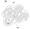


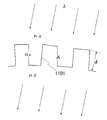

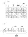

Landscapes
- Surface Treatment Of Optical Elements (AREA)
Priority Applications (1)
| Application Number | Priority Date | Filing Date | Title |
|---|---|---|---|
| JP2011231645A JP2013088757A (ja) | 2011-10-21 | 2011-10-21 | 反射防止構造体 |
Applications Claiming Priority (1)
| Application Number | Priority Date | Filing Date | Title |
|---|---|---|---|
| JP2011231645A JP2013088757A (ja) | 2011-10-21 | 2011-10-21 | 反射防止構造体 |
Publications (2)
| Publication Number | Publication Date |
|---|---|
| JP2013088757A true JP2013088757A (ja) | 2013-05-13 |
| JP2013088757A5 JP2013088757A5 (https=) | 2014-10-30 |
Family
ID=48532689
Family Applications (1)
| Application Number | Title | Priority Date | Filing Date |
|---|---|---|---|
| JP2011231645A Withdrawn JP2013088757A (ja) | 2011-10-21 | 2011-10-21 | 反射防止構造体 |
Country Status (1)
| Country | Link |
|---|---|
| JP (1) | JP2013088757A (https=) |
Cited By (1)
| Publication number | Priority date | Publication date | Assignee | Title |
|---|---|---|---|---|
| JP2015212809A (ja) * | 2014-04-18 | 2015-11-26 | 王子ホールディングス株式会社 | 光学素子 |
Citations (3)
| Publication number | Priority date | Publication date | Assignee | Title |
|---|---|---|---|---|
| JPS574001A (en) * | 1980-06-10 | 1982-01-09 | Sony Corp | Nonreflective optical element |
| JPH11167003A (ja) * | 1997-12-02 | 1999-06-22 | Nikon Corp | 2波長反射防止膜 |
| JP2010131985A (ja) * | 2008-11-07 | 2010-06-17 | Canon Inc | 光学素子成形用金型及び光学素子の成形方法 |
-
2011
- 2011-10-21 JP JP2011231645A patent/JP2013088757A/ja not_active Withdrawn
Patent Citations (3)
| Publication number | Priority date | Publication date | Assignee | Title |
|---|---|---|---|---|
| JPS574001A (en) * | 1980-06-10 | 1982-01-09 | Sony Corp | Nonreflective optical element |
| JPH11167003A (ja) * | 1997-12-02 | 1999-06-22 | Nikon Corp | 2波長反射防止膜 |
| JP2010131985A (ja) * | 2008-11-07 | 2010-06-17 | Canon Inc | 光学素子成形用金型及び光学素子の成形方法 |
Cited By (1)
| Publication number | Priority date | Publication date | Assignee | Title |
|---|---|---|---|---|
| JP2015212809A (ja) * | 2014-04-18 | 2015-11-26 | 王子ホールディングス株式会社 | 光学素子 |
Similar Documents
| Publication | Publication Date | Title |
|---|---|---|
| CN108490509B (zh) | 低深宽比的电介质几何相位超表面材料及其结构优化方法 | |
| Song et al. | Design of highly transparent glasses with broadband antireflective subwavelength structures | |
| JP7199224B2 (ja) | 中空ナノジェットレンズによる近傍界フォーカシング | |
| CN110221447B (zh) | 一种基于超构表面的结构光投影衍射光学器件 | |
| CN114859446B (zh) | 复合超透镜及其形成方法和点阵投影系统 | |
| JP5307307B1 (ja) | シート及び発光装置 | |
| Leem et al. | Enhanced transmittance and hydrophilicity of nanostructured glass substrates with antireflective properties using disordered gold nanopatterns | |
| WO2023093551A1 (zh) | 点云投影系统 | |
| WO2019024572A1 (zh) | 抗反射结构、显示装置及抗反射结构制作方法 | |
| CN107664780B (zh) | 电介质纳米砖阵列结构及其用作高反膜和高透膜的应用 | |
| US20120057235A1 (en) | Method for Antireflection in Binary and Multi-Level Diffractive Elements | |
| JP2009217278A (ja) | 反射防止材、光学素子、および表示装置 | |
| WO2013084900A1 (ja) | 積層体、及び積層体の製造方法 | |
| WO2019196077A1 (zh) | 一种低折射率全介质平面透镜的制作方法 | |
| Dong et al. | Fabrication of hierarchical moth-eye structures with durable superhydrophobic property for ultra-broadband visual and mid-infrared applications | |
| Taha et al. | Textured concave anti-reflecting coating and convex back reflector to enhance the absorbance of amorphous Si solar cells | |
| US20260110913A1 (en) | Embedded transmissive diffractive optical elements | |
| CN103926744A (zh) | 反射膜及其制造方法和显示面板 | |
| JP2003114316A (ja) | 光学素子 | |
| CN105022110A (zh) | 反射式衍射光栅镜和大功率激光器 | |
| JP2013231780A (ja) | 反射防止構造及び光学部材 | |
| JP5780973B2 (ja) | 反射防止膜 | |
| JP2013088757A (ja) | 反射防止構造体 | |
| CN118519328A (zh) | 实现紫外全空间全息像的超表面阵列分布信息获取方法和超表面结构 | |
| Leem et al. | Broadband highly transparent sapphires with biomimetic antireflective compound submicrometer structures for optical and optoelectronic applications |
Legal Events
| Date | Code | Title | Description |
|---|---|---|---|
| A521 | Written amendment |
Free format text: JAPANESE INTERMEDIATE CODE: A523 Effective date: 20140912 |
|
| A621 | Written request for application examination |
Free format text: JAPANESE INTERMEDIATE CODE: A621 Effective date: 20140912 |
|
| A977 | Report on retrieval |
Free format text: JAPANESE INTERMEDIATE CODE: A971007 Effective date: 20150617 |
|
| A131 | Notification of reasons for refusal |
Free format text: JAPANESE INTERMEDIATE CODE: A131 Effective date: 20150623 |
|
| A761 | Written withdrawal of application |
Free format text: JAPANESE INTERMEDIATE CODE: A761 Effective date: 20150713 |