JP2012253390A - Manufacturing method of semiconductor device - Google Patents
Manufacturing method of semiconductor device Download PDFInfo
- Publication number
- JP2012253390A JP2012253390A JP2012209197A JP2012209197A JP2012253390A JP 2012253390 A JP2012253390 A JP 2012253390A JP 2012209197 A JP2012209197 A JP 2012209197A JP 2012209197 A JP2012209197 A JP 2012209197A JP 2012253390 A JP2012253390 A JP 2012253390A
- Authority
- JP
- Japan
- Prior art keywords
- semiconductor chip
- die pad
- recess
- lead frame
- mounting
- Prior art date
- Legal status (The legal status is an assumption and is not a legal conclusion. Google has not performed a legal analysis and makes no representation as to the accuracy of the status listed.)
- Granted
Links
Images


Classifications
-
- H—ELECTRICITY
- H01—ELECTRIC ELEMENTS
- H01L—SEMICONDUCTOR DEVICES NOT COVERED BY CLASS H10
- H01L2224/00—Indexing scheme for arrangements for connecting or disconnecting semiconductor or solid-state bodies and methods related thereto as covered by H01L24/00
- H01L2224/01—Means for bonding being attached to, or being formed on, the surface to be connected, e.g. chip-to-package, die-attach, "first-level" interconnects; Manufacturing methods related thereto
- H01L2224/42—Wire connectors; Manufacturing methods related thereto
- H01L2224/47—Structure, shape, material or disposition of the wire connectors after the connecting process
- H01L2224/48—Structure, shape, material or disposition of the wire connectors after the connecting process of an individual wire connector
- H01L2224/4805—Shape
- H01L2224/4809—Loop shape
- H01L2224/48091—Arched
Abstract
Description
本発明は、半導体チップの搭載位置の確認を容易に行えるリードフレーム、半導体装置、及び半導体装置の製造方法に関する。 The present invention relates to a lead frame, a semiconductor device, and a method for manufacturing a semiconductor device that can easily confirm a mounting position of a semiconductor chip.
半導体チップをリードフレームに実装した半導体装置において、半導体チップをリードフレームのダイパッド上に精度よく載置する必要がある。また、半導体チップの搭載位置の確認を容易に行えるようにすると、不良品を容易に選別できるようになる。 In a semiconductor device in which a semiconductor chip is mounted on a lead frame, it is necessary to accurately place the semiconductor chip on a die pad of the lead frame. Further, if the mounting position of the semiconductor chip can be easily confirmed, defective products can be easily selected.
例えば特許文献1には、ダイアイランド(ダイパッド)に、半導体チップの位置決めの標識となる凹部又は凸部を設ける技術が開示されている。また特許文献2には、ダイパッドにおける半導体チップの載置部の外側に、溝を形成する技術が開示されている。 For example, Patent Document 1 discloses a technique of providing a die island (die pad) with a concave portion or a convex portion serving as a semiconductor chip positioning mark. Patent Document 2 discloses a technique for forming a groove on the outside of a semiconductor chip mounting portion in a die pad.
一つのリードフレームに複数の半導体チップを搭載することがある。また、一種類のリードフレームに互いに異なる半導体チップを搭載することにより、複数種類の半導体装置を製造することがある。これらの場合には、複数種類の半導体チップそれぞれの搭載位置を容易に認識できるようにするのが好ましい。 A plurality of semiconductor chips may be mounted on one lead frame. Further, a plurality of types of semiconductor devices may be manufactured by mounting different semiconductor chips on one type of lead frame. In these cases, it is preferable that the mounting positions of the plurality of types of semiconductor chips can be easily recognized.
本発明によれば、半導体チップが搭載されるダイパッドと、
前記ダイパッドに形成され、第1の半導体チップの搭載領域を示す第1の凹部、凸部、または孔と、
前記ダイパッドに形成され、第2の半導体チップの搭載領域を示す第2の凹部、凸部、または孔と、
を備え、
前記第1の凹部、凸部、または孔と、前記第2の凹部、凸部、または孔は、形状及び大きさの少なくとも一方が異なるリードフレームが提供される。
According to the present invention, a die pad on which a semiconductor chip is mounted;
A first concave portion, a convex portion, or a hole formed on the die pad and indicating a mounting region of the first semiconductor chip;
A second recess, a protrusion, or a hole formed on the die pad and indicating a mounting region of the second semiconductor chip;
With
A lead frame in which at least one of shape and size of the first concave portion, the convex portion, or the hole and the second concave portion, the convex portion, or the hole is different is provided.
この発明によれば、第1の凹部、凸部、または孔と、第2の凹部、凸部、または孔は、形状及び大きさの少なくとも一方が異なる。従って、第1の半導体チップ及び第2の半導体チップそれぞれの搭載位置を容易に認識することができる。 According to this invention, at least one of a shape and a size differs between the first concave portion, the convex portion, or the hole and the second concave portion, the convex portion, or the hole. Therefore, it is possible to easily recognize the mounting positions of the first semiconductor chip and the second semiconductor chip.
本発明によれば、上記したリードフレームと、
前記リードフレームの前記ダイパッドに搭載された前記第1の半導体チップと、
を備える半導体装置が提供される。
According to the present invention, the lead frame described above,
The first semiconductor chip mounted on the die pad of the lead frame;
A semiconductor device is provided.
本発明によれば、第1の半導体チップ及び第2の半導体チップの少なくとも一方を、リードフレームのダイパッド上に搭載する工程と、
前記第1の半導体チップ及び第2の半導体チップの少なくとも一方の搭載位置を検査する工程と、
を有する半導体装置の製造方法であって、
前記リードフレームは、
前記ダイパッドに形成され、前記第1の半導体チップの搭載領域を示す第1の凹部、凸部、または孔と、
前記ダイパッドに形成され、前記第2の半導体チップの搭載領域を示す第2の凹部、凸部、または孔と、
を備え、
前記第1の凹部、凸部、または孔と、前記第2の凹部、凸部、または孔は、形状及び大きさの少なくとも一方が異なり、
前記第1の半導体チップ及び第2の半導体チップの少なくとも一方の搭載位置を検査する工程において、前記第1の半導体チップが搭載されている場合は前記第1の凹部、凸部、または孔と前記第1の半導体チップの相対位置に基づいて前記第1の半導体チップの搭載位置を検査し、前記第2の半導体チップが搭載されている場合は前記第2の凹部、凸部、または孔と前記第2の半導体チップの相対位置に基づいて前記第2の半導体チップの搭載位置を検査する半導体装置の製造方法が提供される。
According to the present invention, a step of mounting at least one of the first semiconductor chip and the second semiconductor chip on the die pad of the lead frame;
Inspecting a mounting position of at least one of the first semiconductor chip and the second semiconductor chip;
A method of manufacturing a semiconductor device having
The lead frame is
A first recess, a protrusion, or a hole formed on the die pad and indicating a mounting region of the first semiconductor chip;
A second recess, protrusion, or hole formed on the die pad and indicating a mounting region of the second semiconductor chip;
With
The first concave portion, convex portion, or hole and the second concave portion, convex portion, or hole are different in at least one of shape and size,
In the step of inspecting the mounting position of at least one of the first semiconductor chip and the second semiconductor chip, when the first semiconductor chip is mounted, the first concave portion, the convex portion, or the hole and the The mounting position of the first semiconductor chip is inspected based on the relative position of the first semiconductor chip, and when the second semiconductor chip is mounted, the second concave portion, the convex portion, or the hole and the A method of manufacturing a semiconductor device is provided that inspects the mounting position of the second semiconductor chip based on the relative position of the second semiconductor chip.
本発明によれば、第1の半導体チップ及び第2の半導体チップそれぞれの搭載位置を容易に認識することができる。 According to the present invention, the mounting positions of the first semiconductor chip and the second semiconductor chip can be easily recognized.
以下、本発明の実施の形態について、図面を用いて説明する。尚、すべての図面において、同様な構成要素には同様の符号を付し、適宜説明を省略する。 Hereinafter, embodiments of the present invention will be described with reference to the drawings. In all the drawings, the same reference numerals are given to the same components, and the description will be omitted as appropriate.
図1は、第1の実施形態にかかる半導体装置の平面図である。この半導体装置は、リードフレーム100、第1の半導体チップ200、及び第2の半導体チップ300を備える。リードフレーム100は、ダイパッド101、第1の凹部112、及び第2の凹部122を備える。ダイパッド101は、第1の半導体チップ200が搭載される。第1の凹部112は第1の半導体チップ200の搭載領域110を示しており、第2の凹部122は第2の半導体チップ300の搭載領域120を示している。第1の凹部112と第2の凹部122は、形状及び大きさの少なくとも一方が異なる。本図に示す例において、第1の凹部112と第2の凹部122は略円形であり、大きさが異なる。具体的には、第1の凹部112は第2の凹部122より大きい。
FIG. 1 is a plan view of the semiconductor device according to the first embodiment. This semiconductor device includes a
第1の凹部112及び第2の凹部122は、例えば径が0.05mm以上0.3mm以下であり、例えば深さが0.01mm以上0.05mm以下である。第1の凹部112及び第2の凹部122は、いずれも第1の半導体チップ200の搭載領域110及び第2の半導体チップ300の搭載領域120の外側に位置している。
The
なお、第1の凹部112の代わりに第1の凸部又は孔を用いても良いし、第2の凹部122の代わりに第2の凸部又は孔を用いても良い。
Note that the first convex portion or hole may be used instead of the first
本図に示す例において第2の半導体チップ300は、第1の半導体チップ200より小さく、第1の半導体チップ200上に搭載されている。そして第2の半導体チップ300の搭載領域120は、第1の半導体チップ200の搭載領域110の内部に位置している。
In the example shown in the drawing, the
ダイパッド101は、略正方形又は略長方形であり、第1の凹部112及び第2の凹部122をそれぞれ複数有している。第1の半導体チップ200の搭載領域110は、隣り合う第1の凹部112を直線で結ぶことにより定義される。また第2の半導体チップ300の搭載領域120は、第1の半導体チップ200の搭載領域110を介して互いに対向する第2の凹部122を直線で結ぶことにより、定義される。
The
本図に示す例において、第1の凹部112で定義された第1の半導体チップ200の搭載領域110は、第1の半導体チップ200より大きく、第1の半導体チップ200の搭載位置の許容範囲を示している。また第2の凹部122で定義された第2の半導体チップ300の搭載領域120も、第2の半導体チップ300より大きく、第2の半導体チップ300の搭載位置の許容範囲を示している。なお、第1の半導体チップ200の搭載領域110が第1の半導体チップ200と同じ形状を有するようにして、搭載領域110が設計上の第1の半導体チップ200の搭載位置を示すようにしてもよい。また第2の半導体チップ300の搭載領域120が第2の半導体チップ300と同じ形状を有するようにして、搭載領域120が設計上の第2の半導体チップ300の搭載位置を示すようにしてもよい。
In the example shown in this figure, the
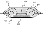
図2は、図1に示した半導体装置の断面図である。本図において半導体装置は、図1に示した構成に加えて、ワイヤ410,420及び封止樹脂500を備えている。ワイヤ410は第1の半導体チップ200のパッド(図示せず)とリードフレーム100のインナーリード(図示せず)とを接続しており、ワイヤ420は第2の半導体チップ300のパッド(図示せず)とリードフレーム100のインナーリード(図示せず)とを接続している。
2 is a cross-sectional view of the semiconductor device shown in FIG. In this figure, the semiconductor device includes
封止樹脂500は、リードフレーム100のダイパッドの表面、インナーリード、第1の半導体チップ200、第2の半導体チップ300、及びワイヤ410,420を封止している。本図に示す例において、封止樹脂500の下面にはリードフレーム100のダイパッド101の下面が露出している。
The sealing
図3は、図2の変形例を示す断面図である。本図に示す半導体装置は、ダイパッド101の下面も封止樹脂500で封止されている点を除いて、図2に示した半導体装置と同様の構成である。
FIG. 3 is a cross-sectional view showing a modification of FIG. The semiconductor device shown in this figure has the same configuration as the semiconductor device shown in FIG. 2 except that the lower surface of the
次に、図1〜3に示した半導体装置の製造方法を説明する。まず、リードフレーム100を準備し、リードフレーム100に第1の凹部112及び第2の凹部122を形成する。第1の凹部112及び第2の凹部122は、例えばジグをリードフレーム100のダイパッド101に上方から押圧することにより、圧痕として形成される。
Next, a method for manufacturing the semiconductor device shown in FIGS. First, the
なお、第1の凹部112及び第2の凹部122の代わりに凸部が用いられる場合、これらの凸部は、例えばジグをリードフレーム100のダイパッド101に下方から押圧することにより、圧痕として形成される。また第1の凹部112及び第2の凹部122の代わりに孔が用いられる場合、孔は、例えば打ち抜きパンチを用いて形成される。
In the case where convex portions are used instead of the first
次いで第1の半導体チップ200をダイパッド101上に搭載し、さらに第2の半導体チップ300を第1の半導体チップ200上に搭載する。ここで第1の半導体チップ200を搭載する装置は、画像処理またはセンサーによって第1の凹部112を認識することにより、第1の半導体チップ200の搭載位置を定める。また第2の半導体チップ300を搭載する装置は、画像処理またはセンサーによって第2の凹部122を認識することにより、第2の半導体チップ300の搭載位置を定める。
Next, the
次いで、ワイヤ410を用いて、第1の半導体チップ200のパッドをリードフレーム100のインナーリードに接続する。また、ワイヤ420を用いて、第2の半導体チップ300のパッドをリードフレーム100のインナーリードに接続する。
Next, the pads of the
次いで、第1の凹部112と第1の半導体チップ200の相対位置に基づいて第1の半導体チップ200の搭載位置を目視で検査し、かつ第2の凹部122と第2の半導体チップ300の相対位置に基づいて第2の半導体チップ300の搭載位置を目視で検査する。詳細には、第1の凹部112により定義される搭載領域110から第1の半導体チップ200がはみ出していない場合に、第1の半導体チップ200の搭載位置は正常であると判断する。また第2の凹部122により定義される搭載領域120から第2の半導体チップ300がはみ出していない場合に、第2の半導体チップ300の搭載位置は正常であると判断する。
Next, the mounting position of the
第1の半導体チップ200の搭載位置及び第2の半導体チップ300の搭載位置の双方が正常であった場合、モールドを用いて封止樹脂500を形成し、リードフレーム100のダイパッド101、インナーリード、第1の半導体チップ200、第2の半導体チップ300、及びワイヤ410,420を封止する。半導体装置が図3に示した構成を有しており、かつ第1の凹部112及び第2の凹部122の代わりに孔が形成されていた場合、この孔内にも封止樹脂500が入り込むため、封止樹脂500とリードフレーム100の密着性が向上する。
When both the mounting position of the
次に、本実施形態の作用効果について説明する。第1の凹部112は第1の半導体チップ200の搭載領域110を示しており、第2の凹部122は第2の半導体チップ300の搭載領域120を示している。第1の凹部112と第2の凹部122は、形状及び大きさの少なくとも一方が異なっている。このため、画像処理またはセンサー並びに目視のいずれの場合においても、第1の半導体チップ200の搭載領域110と、第2の半導体チップ300の搭載領域120それぞれを、容易に認識することができる。
Next, the effect of this embodiment is demonstrated. The
具体的には、半導体チップをダイパッド101に搭載する装置は、第1の半導体チップ200の搭載領域110、及び第2の半導体チップ300の搭載領域120それぞれを容易に認識することができる。また、第1の半導体チップ200及び第2の半導体チップ300それぞれの搭載位置の検査を目視で行う場合においても、第1の半導体チップ200の搭載領域110、及び第2の半導体チップ300の搭載領域120それぞれを容易に認識することができる。
Specifically, the apparatus for mounting the semiconductor chip on the
また、ジグをダイパッド101に押圧することにより、第1の凹部112及び第2の凹部122を形成することができるため、第1の凹部112及び第2の凹部122の形成コストを低くすることができる。
Moreover, since the 1st recessed
また、第1の凹部112及び第2の凹部122はダイパッド101を貫通していないため、ダイパッド101の強度が低下することを抑制でき、また、ダイパッド101の平坦度が低下することを抑制できる。
Moreover, since the 1st recessed
なお、1種類のリードフレーム100を用いて、ダイパッド101に第1の半導体チップ200のみを搭載した第1の半導体装置と、ダイパッド101に第2の半導体チップ300のみを搭載した第2の半導体装置を製造してもよい。このようにすることにより、1種類のリードフレーム100をチップサイズの異なる第1、第2の半導体装置に共用することができる。また、この場合においても上記した効果を得ることができる。
The first semiconductor device in which only the
図4は、第2の実施形態にかかる半導体装置の平面図であり、第1の実施形態における図1に相当する。この半導体装置は、ダイパッド101の平面形状を除いて第1の実施形態に示した半導体装置と同様の構成である。本実施形態において、ダイパッド101は略八角形を有している。
FIG. 4 is a plan view of the semiconductor device according to the second embodiment, and corresponds to FIG. 1 in the first embodiment. This semiconductor device has the same configuration as that of the semiconductor device shown in the first embodiment except for the planar shape of the
本実施形態のようにダイパッド101が複雑な形状を有している場合には、ダイパッド101の端から第1の半導体チップ200及び第2の半導体チップ300の距離がわかりにくい。このため、ダイパッド101の端からの距離に基づいて第1の半導体チップ200及び第2の半導体チップ300の搭載位置を検査することは難しい。これに対して本実施形態は、第1の凹部112によって第1の半導体チップ200の搭載領域110を定めており、かつ第2の凹部122によって第2の半導体チップ300の搭載領域120を定めている。このため、容易に第1の半導体チップ200及び第2の半導体チップ300の搭載位置を検査することができる。
When the
図5は、第3の実施形態にかかる半導体装置の平面図であり、第1の実施形態における図1に相当する。この半導体装置は、第1の凹部112と第2の凹部122の形状が異なる点を除いて、第1の実施形態と同様の効果を得ることができる。
FIG. 5 is a plan view of the semiconductor device according to the third embodiment, and corresponds to FIG. 1 in the first embodiment. This semiconductor device can obtain the same effects as those of the first embodiment except that the shapes of the
本実施形態によっても、第1の実施形態と同様の効果を得ることができる。また、第1の凹部112と第2の凹部122を同じ大きさにすることができるため、第1の凹部112及び第2の凹部122のいずれも目視で確認しやすくなる。
Also according to this embodiment, the same effect as that of the first embodiment can be obtained. Moreover, since the 1st recessed
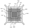
図6は、第4の実施形態にかかる半導体装置の平面図であり、第1の実施形態における図1に相当する。この半導体装置は、第2の半導体チップ300の上に第3の半導体チップ600が搭載されている点、及びダイパッド101に複数の第3の凹部132が形成されている点を除いて、第1の実施形態にかかる半導体装置と同様の構成である。第3の凹部132は、第1の凹部112及び第2の凹部122と同一工程で形成される。
FIG. 6 is a plan view of the semiconductor device according to the fourth embodiment, and corresponds to FIG. 1 in the first embodiment. This semiconductor device is the first except that the
第3の半導体チップ600は第2の半導体チップ300より小さい。第3の凹部132は、第1の凹部112及び第2の凹部122の双方と、形状及び大きさのいずれか一方が異なる。また複数の第3の凹部132は、第3の半導体チップ600の搭載領域130を示している。搭載領域130は、第2の半導体チップ300の搭載領域120を介して互いに対向する第3の凹部132を直線で結ぶことにより、定義される。
The
本実施形態によっても、第1の実施形態と同様の効果を得ることができる。また、第3の半導体チップ600の搭載及び搭載位置の検査も、第1の半導体チップ200及び第2の半導体チップ300の搭載及び搭載位置の検査と同様に行うことができる。
Also according to this embodiment, the same effect as that of the first embodiment can be obtained. Further, the mounting of the
図7は、第5の実施形態にかかる半導体装置の平面図であり、第4の実施形態における図6に相当する。この半導体装置は、第2の半導体チップ300及び第3の半導体チップ600の双方が第1の半導体チップ200の上に搭載されている点を除いて、第4の実施形態と同様の構成である。
本実施形態によっても第4の実施形態と同様の効果を得ることができる。
FIG. 7 is a plan view of the semiconductor device according to the fifth embodiment, and corresponds to FIG. 6 in the fourth embodiment. This semiconductor device has the same configuration as that of the fourth embodiment except that both the
According to this embodiment, the same effect as that of the fourth embodiment can be obtained.
図8は、第6の実施形態にかかる半導体装置の平面図であり、第1の実施形態における図1に相当する。この半導体装置は、第2の半導体チップ300が第1の半導体チップ200上ではなくリードフレーム100のダイパッド101上に搭載されている点を除いて、第1の実施形態と同様の構成である。
本実施形態においても第1の実施形態と同様の効果を得ることができる。
FIG. 8 is a plan view of the semiconductor device according to the sixth embodiment, and corresponds to FIG. 1 in the first embodiment. This semiconductor device has the same configuration as that of the first embodiment except that the
In this embodiment, the same effect as that of the first embodiment can be obtained.
図9は第7の実施形態にかかる半導体装置の平面図であり、図10は図9に示した半導体装置の断面概略図である。この半導体装置は、以下の点を除いて第1の実施形態と同様の構成である。まず、第1の半導体チップ200がリードフレーム100のダイパッド101の第1面上に搭載されており、第2の半導体チップ300がダイパッド101の第1面とは反対側の面である第2面上に搭載されている。そして第1の凹部112がダイパッド101の第1面に形成されており、第2の凹部122がダイパッド101の第2面に形成されている。
FIG. 9 is a plan view of the semiconductor device according to the seventh embodiment, and FIG. 10 is a schematic cross-sectional view of the semiconductor device shown in FIG. This semiconductor device has the same configuration as that of the first embodiment except for the following points. First, the
本実施形態によれば、ダイパッド101の第1面に形成された第1の凹部112と、ダイパッド101の第2面に形成された第2の凹部122は、形状及び大きさの少なくとも一方が異なる。このため、第1の半導体チップ200を搭載すべき面、及び第2の半導体チップ300を搭載すべき面それぞれを容易に把握することができる。従って、第1の半導体チップ200の搭載面と第2の半導体チップ300の搭載面を間違える可能性が低くなる。
According to this embodiment, the
図11は第8の実施形態にかかる半導体装置の平面図であり、図12は図11に示した半導体装置の断面概略図である。この半導体装置は、以下の点を除いて、第4の実施形態と同様の構成である。まず、リードフレーム100のダイパッド101の第1面上には、第1の半導体チップ200及び第2の半導体チップ300が搭載されている。ダイパッド101の第1面とは反対側の面である第2面上には、第3の半導体チップ600が搭載されている。また、ダイパッド101の第1面には第1の凹部112及び第2の凹部122が形成されており、ダイパッド101の第2面には第3の凹部132が形成されている。
FIG. 11 is a plan view of the semiconductor device according to the eighth embodiment, and FIG. 12 is a schematic cross-sectional view of the semiconductor device shown in FIG. This semiconductor device has the same configuration as that of the fourth embodiment except for the following points. First, the
図12に示すように、本実施形態において第2の半導体チップ300は、一部のワイヤ420を介してリードフレーム100に直接接続しており、残りのワイヤ420を介して第1の半導体チップ200に接続している。また第3の半導体チップ600は、ワイヤ430を介してリードフレーム100に直接接続している。
As shown in FIG. 12, in the present embodiment, the
本実施形態によっても第4の実施形態と同様の効果を得ることができる。また、ダイパッド101の第1面に形成された第1の凹部112及び第2の凹部122と、ダイパッド101の第2面に形成された第3の凹部132は、形状及び大きさの少なくとも一方が異なる。このため、第1の半導体チップ200及び第2の半導体チップ300を搭載すべき面と第3の半導体チップ600を搭載すべき面それぞれを容易に把握することができる。従って、第1の半導体チップ200及び第2の半導体チップ300の搭載面、並びに第3の半導体チップ600の搭載面を間違える可能性が低くなる。
According to this embodiment, the same effect as that of the fourth embodiment can be obtained. Further, the first and
なお第7の実施形態において、第1の凹部112と第2の凹部122は大きさ及び形状が同じであっても良い。また第8の実施形態において、第3の凹部132は、第1の凹部112又は第2の凹部122と大きさ及び形状が同じであっても良い。
In the seventh embodiment, the
以上、図面を参照して本発明の実施形態について述べたが、これらは本発明の例示であり、上記以外の様々な構成を採用することもできる。 As mentioned above, although embodiment of this invention was described with reference to drawings, these are the illustrations of this invention, Various structures other than the above are also employable.
100 リードフレーム
101 ダイパッド
110 第1の半導体チップの搭載領域
112 第1の凹部
120 第2の半導体チップの搭載領域
122 第2の凹部
130 第3の半導体チップの搭載領域
132 第3の凹部
200 第1の半導体チップ
300 第2の半導体チップ
410 ワイヤ
420 ワイヤ
430 ワイヤ
500 封止樹脂
600 第3の半導体チップ
100
以上、図面を参照して本発明の実施形態について述べたが、これらは本発明の例示であり、上記以外の様々な構成を採用することもできる。
(付記1)
半導体チップが搭載されるダイパッドと、
前記ダイパッドに形成され、第1の半導体チップの搭載領域を示す第1の凹部、凸部、または孔と、
前記ダイパッドに形成され、第2の半導体チップの搭載領域を示す第2の凹部、凸部、または孔と、
を備え、
前記第1の凹部、凸部、または孔と、前記第2の凹部、凸部、または孔は、形状及び大きさの少なくとも一方が異なるリードフレーム。
(付記2)
付記1に記載のリードフレームにおいて、
前記第2の半導体チップは、前記第1の半導体チップより小さく、かつ前記第1の半導体チップ上に搭載され、
前記ダイパッドにおいて、前記第2の半導体チップの搭載領域は、前記第1の半導体チップの搭載領域の内部に位置するリードフレーム。
(付記3)
付記2に記載のリードフレームにおいて、
前記第1の凹部、凸部、または孔と、前記第2の凹部、凸部、または孔とを、それぞれ複数有しており、
隣り合う前記第1の凹部、凸部、または孔を結ぶことにより、前記第1の半導体チップの搭載領域が定義され、
前記第1の半導体チップの搭載領域を介して互いに対向する前記第2の凹部、凸部、または孔を結ぶことにより、前記第2の半導体チップの搭載領域が定義されるリードフレーム。
(付記4)
付記1に記載のリードフレームにおいて、
前記第1の凹部、凸部、または孔は、前記ダイパッドの第1面に形成され、
前記第2の凹部、凸部、または孔は、前記ダイパッドの第1面とは反対側の面である第2面に形成されているリードフレーム。
(付記5)
付記2に記載のリードフレームにおいて、
前記第1の凹部、凸部、または孔、並びに前記第2の凹部、凸部、または孔は、前記ダイパッドの第1面に形成され、
さらに、前記ダイパッドの第1面とは反対側の面である第2面に形成されており、第3の半導体チップの搭載領域を示す第3の凹部、凸部、または孔を備えるリードフレーム。
(付記6)
付記1〜5のいずれか一つに記載のリードフレームと、
前記リードフレームの前記ダイパッドに搭載された前記第1の半導体チップと、
を備える半導体装置。
(付記7)
第1の半導体チップ及び第2の半導体チップの少なくとも一方を、リードフレームのダイパッド上に搭載する工程と、
前記第1の半導体チップ及び第2の半導体チップの少なくとも一方の搭載位置を検査する工程と、
を有する半導体装置の製造方法であって、
前記リードフレームは、
前記ダイパッドに形成され、前記第1の半導体チップの搭載領域を示す第1の凹部、凸部、または孔と、
前記ダイパッドに形成され、前記第2の半導体チップの搭載領域を示す第2の凹部、凸部、または孔と、
を備え、
前記第1の凹部、凸部、または孔と、前記第2の凹部、凸部、または孔は、形状及び大きさの少なくとも一方が異なり、
前記第1の半導体チップ及び第2の半導体チップの少なくとも一方の搭載位置を検査する工程において、前記第1の半導体チップが搭載されている場合は前記第1の凹部、凸部、または孔と前記第1の半導体チップの相対位置に基づいて前記第1の半導体チップの搭載位置を検査し、前記第2の半導体チップが搭載されている場合は前記第2の凹部、凸部、または孔と前記第2の半導体チップの相対位置に基づいて前記第2の半導体チップの搭載位置を検査する半導体装置の製造方法。
(付記8)
付記7に記載の半導体装置の製造方法において、
前記第1の半導体チップは前記第2の半導体チップより大きく、
前記第1の半導体チップ及び第2の半導体チップの少なくとも一方を前記ダイパッド上に搭載する工程において、前記第1の半導体チップを前記ダイパッド上に搭載し、かつ前記第2の半導体チップを前記第1の半導体チップ上に搭載する半導体装置の製造方法。
(付記9)
付記8に記載の半導体装置の製造方法において、
前記リードフレームは、前記第1の凹部、凸部、または孔と、前記第2の凹部、凸部、または孔とを、それぞれ複数有しており、
隣り合う前記第1の凹部、凸部、または孔を結ぶことにより、前記第1の半導体チップの搭載領域が定義され、
前記第1の半導体チップの搭載領域を介して互いに対向する前記第2の凹部、凸部、または孔を結ぶことにより、前記第2の半導体チップの搭載領域が定義される半導体装置の製造方法。
As mentioned above, although embodiment of this invention was described with reference to drawings, these are the illustrations of this invention, Various structures other than the above are also employable.
(Appendix 1)
A die pad on which a semiconductor chip is mounted;
A first concave portion, a convex portion, or a hole formed on the die pad and indicating a mounting region of the first semiconductor chip;
A second recess, a protrusion, or a hole formed on the die pad and indicating a mounting region of the second semiconductor chip;
With
The first concave portion, convex portion, or hole and the second concave portion, convex portion, or hole are lead frames that are different in at least one of shape and size.
(Appendix 2)
In the lead frame described in Appendix 1,
The second semiconductor chip is smaller than the first semiconductor chip and mounted on the first semiconductor chip;
In the die pad, the mounting area of the second semiconductor chip is a lead frame located inside the mounting area of the first semiconductor chip.
(Appendix 3)
In the lead frame described in Appendix 2,
Each having a plurality of the first recesses, projections, or holes, and the second recesses, projections, or holes;
A mounting region of the first semiconductor chip is defined by connecting adjacent first concave portions, convex portions, or holes,
A lead frame in which a mounting region of the second semiconductor chip is defined by connecting the second recesses, protrusions, or holes facing each other through the mounting region of the first semiconductor chip.
(Appendix 4)
In the lead frame described in Appendix 1,
The first concave portion, the convex portion, or the hole is formed on the first surface of the die pad,
The second concave portion, the convex portion, or the hole is a lead frame formed on a second surface that is a surface opposite to the first surface of the die pad.
(Appendix 5)
In the lead frame described in Appendix 2,
The first concave portion, convex portion, or hole, and the second concave portion, convex portion, or hole are formed on the first surface of the die pad,
Furthermore, the lead frame is provided on a second surface which is a surface opposite to the first surface of the die pad, and includes a third recess, a protrusion, or a hole indicating a mounting region of a third semiconductor chip.
(Appendix 6)
The lead frame according to any one of appendices 1 to 5,
The first semiconductor chip mounted on the die pad of the lead frame;
A semiconductor device comprising:
(Appendix 7)
Mounting at least one of the first semiconductor chip and the second semiconductor chip on a die pad of a lead frame;
Inspecting a mounting position of at least one of the first semiconductor chip and the second semiconductor chip;
A method of manufacturing a semiconductor device having
The lead frame is
A first recess, a protrusion, or a hole formed on the die pad and indicating a mounting region of the first semiconductor chip;
A second recess, protrusion, or hole formed on the die pad and indicating a mounting region of the second semiconductor chip;
With
The first concave portion, convex portion, or hole and the second concave portion, convex portion, or hole are different in at least one of shape and size,
In the step of inspecting the mounting position of at least one of the first semiconductor chip and the second semiconductor chip, when the first semiconductor chip is mounted, the first concave portion, the convex portion, or the hole and the The mounting position of the first semiconductor chip is inspected based on the relative position of the first semiconductor chip, and when the second semiconductor chip is mounted, the second concave portion, the convex portion, or the hole and the A method of manufacturing a semiconductor device, wherein a mounting position of the second semiconductor chip is inspected based on a relative position of the second semiconductor chip.
(Appendix 8)
In the method for manufacturing a semiconductor device according to attachment 7,
The first semiconductor chip is larger than the second semiconductor chip;
In the step of mounting at least one of the first semiconductor chip and the second semiconductor chip on the die pad, the first semiconductor chip is mounted on the die pad, and the second semiconductor chip is mounted on the first pad. Of manufacturing a semiconductor device mounted on a semiconductor chip.
(Appendix 9)
In the method for manufacturing a semiconductor device according to attachment 8,
The lead frame has a plurality of the first concave portions, convex portions, or holes, and the second concave portions, convex portions, or holes, respectively.
A mounting region of the first semiconductor chip is defined by connecting adjacent first concave portions, convex portions, or holes,
A method of manufacturing a semiconductor device, wherein the second semiconductor chip mounting region is defined by connecting the second recesses, protrusions, or holes facing each other through the mounting region of the first semiconductor chip.
Claims (9)
前記ダイパッドに形成され、第1の半導体チップの搭載領域を示す第1の凹部、凸部、または孔と、
前記ダイパッドに形成され、第2の半導体チップの搭載領域を示す第2の凹部、凸部、または孔と、
を備え、
前記第1の凹部、凸部、または孔と、前記第2の凹部、凸部、または孔は、形状及び大きさの少なくとも一方が異なるリードフレーム。 A die pad on which a semiconductor chip is mounted;
A first concave portion, a convex portion, or a hole formed on the die pad and indicating a mounting region of the first semiconductor chip;
A second recess, a protrusion, or a hole formed on the die pad and indicating a mounting region of the second semiconductor chip;
With
The first concave portion, convex portion, or hole and the second concave portion, convex portion, or hole are lead frames that are different in at least one of shape and size.
前記第2の半導体チップは、前記第1の半導体チップより小さく、かつ前記第1の半導体チップ上に搭載され、
前記ダイパッドにおいて、前記第2の半導体チップの搭載領域は、前記第1の半導体チップの搭載領域の内部に位置するリードフレーム。 The lead frame according to claim 1,
The second semiconductor chip is smaller than the first semiconductor chip and mounted on the first semiconductor chip;
In the die pad, the mounting area of the second semiconductor chip is a lead frame located inside the mounting area of the first semiconductor chip.
前記第1の凹部、凸部、または孔と、前記第2の凹部、凸部、または孔とを、それぞれ複数有しており、
隣り合う前記第1の凹部、凸部、または孔を結ぶことにより、前記第1の半導体チップの搭載領域が定義され、
前記第1の半導体チップの搭載領域を介して互いに対向する前記第2の凹部、凸部、または孔を結ぶことにより、前記第2の半導体チップの搭載領域が定義されるリードフレーム。 The lead frame according to claim 2,
Each having a plurality of the first recesses, projections, or holes, and the second recesses, projections, or holes;
A mounting region of the first semiconductor chip is defined by connecting adjacent first concave portions, convex portions, or holes,
A lead frame in which a mounting region of the second semiconductor chip is defined by connecting the second recesses, protrusions, or holes facing each other through the mounting region of the first semiconductor chip.
前記第1の凹部、凸部、または孔は、前記ダイパッドの第1面に形成され、
前記第2の凹部、凸部、または孔は、前記ダイパッドの第1面とは反対側の面である第2面に形成されているリードフレーム。 The lead frame according to claim 1,
The first concave portion, the convex portion, or the hole is formed on the first surface of the die pad,
The second concave portion, the convex portion, or the hole is a lead frame formed on a second surface that is a surface opposite to the first surface of the die pad.
前記第1の凹部、凸部、または孔、並びに前記第2の凹部、凸部、または孔は、前記ダイパッドの第1面に形成され、
さらに、前記ダイパッドの第1面とは反対側の面である第2面に形成されており、第3の半導体チップの搭載領域を示す第3の凹部、凸部、または孔を備えるリードフレーム。 The lead frame according to claim 2,
The first concave portion, convex portion, or hole, and the second concave portion, convex portion, or hole are formed on the first surface of the die pad,
Furthermore, the lead frame is provided on a second surface which is a surface opposite to the first surface of the die pad, and includes a third recess, a protrusion, or a hole indicating a mounting region of a third semiconductor chip.
前記リードフレームの前記ダイパッドに搭載された前記第1の半導体チップと、
を備える半導体装置。 A lead frame according to any one of claims 1 to 5;
The first semiconductor chip mounted on the die pad of the lead frame;
A semiconductor device comprising:
前記第1の半導体チップ及び第2の半導体チップの少なくとも一方の搭載位置を検査する工程と、
を有する半導体装置の製造方法であって、
前記リードフレームは、
前記ダイパッドに形成され、前記第1の半導体チップの搭載領域を示す第1の凹部、凸部、または孔と、
前記ダイパッドに形成され、前記第2の半導体チップの搭載領域を示す第2の凹部、凸部、または孔と、
を備え、
前記第1の凹部、凸部、または孔と、前記第2の凹部、凸部、または孔は、形状及び大きさの少なくとも一方が異なり、
前記第1の半導体チップ及び第2の半導体チップの少なくとも一方の搭載位置を検査する工程において、前記第1の半導体チップが搭載されている場合は前記第1の凹部、凸部、または孔と前記第1の半導体チップの相対位置に基づいて前記第1の半導体チップの搭載位置を検査し、前記第2の半導体チップが搭載されている場合は前記第2の凹部、凸部、または孔と前記第2の半導体チップの相対位置に基づいて前記第2の半導体チップの搭載位置を検査する半導体装置の製造方法。 Mounting at least one of the first semiconductor chip and the second semiconductor chip on a die pad of a lead frame;
Inspecting a mounting position of at least one of the first semiconductor chip and the second semiconductor chip;
A method of manufacturing a semiconductor device having
The lead frame is
A first recess, a protrusion, or a hole formed on the die pad and indicating a mounting region of the first semiconductor chip;
A second recess, protrusion, or hole formed on the die pad and indicating a mounting region of the second semiconductor chip;
With
The first concave portion, convex portion, or hole and the second concave portion, convex portion, or hole are different in at least one of shape and size,
In the step of inspecting the mounting position of at least one of the first semiconductor chip and the second semiconductor chip, when the first semiconductor chip is mounted, the first concave portion, the convex portion, or the hole and the The mounting position of the first semiconductor chip is inspected based on the relative position of the first semiconductor chip, and when the second semiconductor chip is mounted, the second concave portion, the convex portion, or the hole and the A method of manufacturing a semiconductor device, wherein a mounting position of the second semiconductor chip is inspected based on a relative position of the second semiconductor chip.
前記第1の半導体チップは前記第2の半導体チップより大きく、
前記第1の半導体チップ及び第2の半導体チップの少なくとも一方を前記ダイパッド上に搭載する工程において、前記第1の半導体チップを前記ダイパッド上に搭載し、かつ前記第2の半導体チップを前記第1の半導体チップ上に搭載する半導体装置の製造方法。 In the manufacturing method of the semiconductor device according to claim 7,
The first semiconductor chip is larger than the second semiconductor chip;
In the step of mounting at least one of the first semiconductor chip and the second semiconductor chip on the die pad, the first semiconductor chip is mounted on the die pad, and the second semiconductor chip is mounted on the first pad. Of manufacturing a semiconductor device mounted on a semiconductor chip.
前記リードフレームは、前記第1の凹部、凸部、または孔と、前記第2の凹部、凸部、または孔とを、それぞれ複数有しており、
隣り合う前記第1の凹部、凸部、または孔を結ぶことにより、前記第1の半導体チップの搭載領域が定義され、
前記第1の半導体チップの搭載領域を介して互いに対向する前記第2の凹部、凸部、または孔を結ぶことにより、前記第2の半導体チップの搭載領域が定義される半導体装置の製造方法。 In the manufacturing method of the semiconductor device according to claim 8,
The lead frame has a plurality of the first concave portions, convex portions, or holes, and the second concave portions, convex portions, or holes, respectively.
A mounting region of the first semiconductor chip is defined by connecting adjacent first concave portions, convex portions, or holes,
A method of manufacturing a semiconductor device, wherein the second semiconductor chip mounting region is defined by connecting the second recesses, protrusions, or holes facing each other through the mounting region of the first semiconductor chip.
Priority Applications (1)
| Application Number | Priority Date | Filing Date | Title |
|---|---|---|---|
| JP2012209197A JP5566433B2 (en) | 2012-09-24 | 2012-09-24 | Manufacturing method of semiconductor device |
Applications Claiming Priority (1)
| Application Number | Priority Date | Filing Date | Title |
|---|---|---|---|
| JP2012209197A JP5566433B2 (en) | 2012-09-24 | 2012-09-24 | Manufacturing method of semiconductor device |
Related Parent Applications (1)
| Application Number | Title | Priority Date | Filing Date |
|---|---|---|---|
| JP2008199186A Division JP5097639B2 (en) | 2008-08-01 | 2008-08-01 | Lead frame and semiconductor device |
Publications (2)
| Publication Number | Publication Date |
|---|---|
| JP2012253390A true JP2012253390A (en) | 2012-12-20 |
| JP5566433B2 JP5566433B2 (en) | 2014-08-06 |
Family
ID=47525847
Family Applications (1)
| Application Number | Title | Priority Date | Filing Date |
|---|---|---|---|
| JP2012209197A Active JP5566433B2 (en) | 2012-09-24 | 2012-09-24 | Manufacturing method of semiconductor device |
Country Status (1)
| Country | Link |
|---|---|
| JP (1) | JP5566433B2 (en) |
Cited By (4)
| Publication number | Priority date | Publication date | Assignee | Title |
|---|---|---|---|---|
| JP2017085049A (en) * | 2015-10-30 | 2017-05-18 | 新光電気工業株式会社 | Semiconductor device and method of manufacturing the same, lead frame and method of manufacturing the same |
| JP2017199823A (en) * | 2016-04-28 | 2017-11-02 | 株式会社ジェイデバイス | Semiconductor package and method of manufacturing the same |
| CN107507779A (en) * | 2016-06-14 | 2017-12-22 | 株式会社吉帝伟士 | The manufacture method of semiconductor package part |
| WO2021111517A1 (en) * | 2019-12-03 | 2021-06-10 | 太陽誘電株式会社 | Component module and manufacturing method therefor |
Citations (8)
| Publication number | Priority date | Publication date | Assignee | Title |
|---|---|---|---|---|
| JPS5684360U (en) * | 1979-11-29 | 1981-07-07 | ||
| JPS5818948A (en) * | 1981-07-27 | 1983-02-03 | Toshiba Corp | Lead frame |
| JPS62163962U (en) * | 1986-04-08 | 1987-10-17 | ||
| JPH02253649A (en) * | 1989-03-27 | 1990-10-12 | Nec Kyushu Ltd | Lead frame for semiconductor device |
| JPH1126689A (en) * | 1997-06-30 | 1999-01-29 | Sanyo Electric Co Ltd | Semiconductor device |
| JP2001144247A (en) * | 1999-11-12 | 2001-05-25 | Mitsui High Tec Inc | Semiconductor device |
| JP2002261229A (en) * | 2001-03-02 | 2002-09-13 | Hitachi Ltd | Method of manufacturing semiconductor device |
| JP2008124116A (en) * | 2006-11-09 | 2008-05-29 | Denso Corp | Semiconductor device |
-
2012
- 2012-09-24 JP JP2012209197A patent/JP5566433B2/en active Active
Patent Citations (8)
| Publication number | Priority date | Publication date | Assignee | Title |
|---|---|---|---|---|
| JPS5684360U (en) * | 1979-11-29 | 1981-07-07 | ||
| JPS5818948A (en) * | 1981-07-27 | 1983-02-03 | Toshiba Corp | Lead frame |
| JPS62163962U (en) * | 1986-04-08 | 1987-10-17 | ||
| JPH02253649A (en) * | 1989-03-27 | 1990-10-12 | Nec Kyushu Ltd | Lead frame for semiconductor device |
| JPH1126689A (en) * | 1997-06-30 | 1999-01-29 | Sanyo Electric Co Ltd | Semiconductor device |
| JP2001144247A (en) * | 1999-11-12 | 2001-05-25 | Mitsui High Tec Inc | Semiconductor device |
| JP2002261229A (en) * | 2001-03-02 | 2002-09-13 | Hitachi Ltd | Method of manufacturing semiconductor device |
| JP2008124116A (en) * | 2006-11-09 | 2008-05-29 | Denso Corp | Semiconductor device |
Cited By (6)
| Publication number | Priority date | Publication date | Assignee | Title |
|---|---|---|---|---|
| JP2017085049A (en) * | 2015-10-30 | 2017-05-18 | 新光電気工業株式会社 | Semiconductor device and method of manufacturing the same, lead frame and method of manufacturing the same |
| JP2017199823A (en) * | 2016-04-28 | 2017-11-02 | 株式会社ジェイデバイス | Semiconductor package and method of manufacturing the same |
| CN107424980A (en) * | 2016-04-28 | 2017-12-01 | 株式会社吉帝伟士 | The manufacture method of semiconductor package part and semiconductor package part |
| US10553456B2 (en) | 2016-04-28 | 2020-02-04 | J-Devices Corporation | Semiconductor package and manufacturing method of semiconductor package |
| CN107507779A (en) * | 2016-06-14 | 2017-12-22 | 株式会社吉帝伟士 | The manufacture method of semiconductor package part |
| WO2021111517A1 (en) * | 2019-12-03 | 2021-06-10 | 太陽誘電株式会社 | Component module and manufacturing method therefor |
Also Published As
| Publication number | Publication date |
|---|---|
| JP5566433B2 (en) | 2014-08-06 |
Similar Documents
| Publication | Publication Date | Title |
|---|---|---|
| JP5097639B2 (en) | Lead frame and semiconductor device | |
| JP5566433B2 (en) | Manufacturing method of semiconductor device | |
| TWI409926B (en) | Leadframe | |
| US9448216B2 (en) | Gas sensor device with frame passageways and related methods | |
| US9620388B2 (en) | Integrated circuit package fabrication with die attach paddle having middle channels | |
| TW201546987A (en) | Semiconductor device and method of manufacturing the same | |
| WO2015088658A3 (en) | Integrated wire bonder and 3d measurement system with defect rejection | |
| JP2018056369A (en) | Semiconductor device manufacturing method | |
| US11756919B2 (en) | Wedge tool, bonding device, and bonding inspection method | |
| US9202778B2 (en) | Integrated circuit package with die attach paddle having at least one recessed portion | |
| JP5701579B2 (en) | Manufacturing method of semiconductor device | |
| JP2007294568A (en) | Semiconductor device | |
| JP2016201447A (en) | Molded package | |
| JP3144633U (en) | Lead frame and semiconductor device | |
| JP2010087173A (en) | Method of manufacturing semiconductor device, and semiconductor device | |
| JP5971171B2 (en) | Insulating substrate, manufacturing method thereof, and semiconductor device | |
| CN106469689A (en) | Electronic component and forming method thereof | |
| CN103972187A (en) | Chip package and manufacturing method thereof | |
| KR20090033121A (en) | Semiconductor device | |
| US11600557B2 (en) | Packaged device having selective lead pullback for dimple depth control | |
| JP2010197309A (en) | Mems sensor, and method for manufacturing the same | |
| JP2008166351A (en) | Semiconductor device | |
| JP5911615B2 (en) | Lead frame | |
| JP2007294637A (en) | Method for manufacturing semiconductor device | |
| JP2009218493A (en) | Method for confirming junction state of wire bonding |
Legal Events
| Date | Code | Title | Description |
|---|---|---|---|
| A521 | Written amendment |
Free format text: JAPANESE INTERMEDIATE CODE: A523 Effective date: 20120924 |
|
| A621 | Written request for application examination |
Free format text: JAPANESE INTERMEDIATE CODE: A621 Effective date: 20120924 |
|
| A977 | Report on retrieval |
Free format text: JAPANESE INTERMEDIATE CODE: A971007 Effective date: 20130823 |
|
| A131 | Notification of reasons for refusal |
Free format text: JAPANESE INTERMEDIATE CODE: A131 Effective date: 20130903 |
|
| A521 | Written amendment |
Free format text: JAPANESE INTERMEDIATE CODE: A523 Effective date: 20131018 |
|
| TRDD | Decision of grant or rejection written | ||
| A01 | Written decision to grant a patent or to grant a registration (utility model) |
Free format text: JAPANESE INTERMEDIATE CODE: A01 Effective date: 20140527 |
|
| A61 | First payment of annual fees (during grant procedure) |
Free format text: JAPANESE INTERMEDIATE CODE: A61 Effective date: 20140617 |
|
| R150 | Certificate of patent or registration of utility model |
Ref document number: 5566433 Country of ref document: JP Free format text: JAPANESE INTERMEDIATE CODE: R150 |
|
| S531 | Written request for registration of change of domicile |
Free format text: JAPANESE INTERMEDIATE CODE: R313531 |
|
| R350 | Written notification of registration of transfer |
Free format text: JAPANESE INTERMEDIATE CODE: R350 |