JP2012233903A - 表面増強赤外吸収センサーの製造方法 - Google Patents
表面増強赤外吸収センサーの製造方法 Download PDFInfo
- Publication number
- JP2012233903A JP2012233903A JP2012144529A JP2012144529A JP2012233903A JP 2012233903 A JP2012233903 A JP 2012233903A JP 2012144529 A JP2012144529 A JP 2012144529A JP 2012144529 A JP2012144529 A JP 2012144529A JP 2012233903 A JP2012233903 A JP 2012233903A
- Authority
- JP
- Japan
- Prior art keywords
- thin films
- infrared absorption
- metal
- seira
- enhanced infrared
- Prior art date
- Legal status (The legal status is an assumption and is not a legal conclusion. Google has not performed a legal analysis and makes no representation as to the accuracy of the status listed.)
- Granted
Links
- 238000010521 absorption reaction Methods 0.000 title claims abstract description 53
- 238000000034 method Methods 0.000 title claims abstract description 49
- 238000004519 manufacturing process Methods 0.000 title claims abstract description 41
- 239000010409 thin film Substances 0.000 claims abstract description 48
- 239000000758 substrate Substances 0.000 claims abstract description 31
- 238000011065 in-situ storage Methods 0.000 claims abstract description 14
- 230000008859 change Effects 0.000 claims abstract description 13
- 238000000862 absorption spectrum Methods 0.000 claims abstract description 10
- 239000002082 metal nanoparticle Substances 0.000 claims abstract description 8
- 239000002184 metal Substances 0.000 claims description 46
- 229910052751 metal Inorganic materials 0.000 claims description 46
- 230000035945 sensitivity Effects 0.000 abstract description 13
- 238000012544 monitoring process Methods 0.000 abstract description 11
- 230000001678 irradiating effect Effects 0.000 abstract 1
- 239000010408 film Substances 0.000 description 48
- 239000010931 gold Substances 0.000 description 46
- 239000000463 material Substances 0.000 description 38
- 230000000694 effects Effects 0.000 description 28
- 239000002105 nanoparticle Substances 0.000 description 27
- 239000002245 particle Substances 0.000 description 25
- 238000001179 sorption measurement Methods 0.000 description 18
- KRKNYBCHXYNGOX-UHFFFAOYSA-N citric acid Chemical compound OC(=O)CC(O)(C(O)=O)CC(O)=O KRKNYBCHXYNGOX-UHFFFAOYSA-N 0.000 description 15
- XUIMIQQOPSSXEZ-UHFFFAOYSA-N Silicon Chemical compound [Si] XUIMIQQOPSSXEZ-UHFFFAOYSA-N 0.000 description 12
- 229910052710 silicon Inorganic materials 0.000 description 12
- 239000010703 silicon Substances 0.000 description 12
- 238000005259 measurement Methods 0.000 description 10
- XLYOFNOQVPJJNP-ZSJDYOACSA-N Heavy water Chemical compound [2H]O[2H] XLYOFNOQVPJJNP-ZSJDYOACSA-N 0.000 description 8
- 239000013078 crystal Substances 0.000 description 8
- 230000005684 electric field Effects 0.000 description 8
- 238000004415 surface enhanced infrared absorption spectroscopy Methods 0.000 description 7
- 238000001228 spectrum Methods 0.000 description 6
- WYTZZXDRDKSJID-UHFFFAOYSA-N (3-aminopropyl)triethoxysilane Chemical group CCO[Si](OCC)(OCC)CCCN WYTZZXDRDKSJID-UHFFFAOYSA-N 0.000 description 5
- 239000006087 Silane Coupling Agent Substances 0.000 description 5
- QJAOYSPHSNGHNC-UHFFFAOYSA-N octadecane-1-thiol Chemical compound CCCCCCCCCCCCCCCCCCS QJAOYSPHSNGHNC-UHFFFAOYSA-N 0.000 description 5
- 239000000126 substance Substances 0.000 description 5
- XLYOFNOQVPJJNP-UHFFFAOYSA-N water Substances O XLYOFNOQVPJJNP-UHFFFAOYSA-N 0.000 description 5
- 238000010586 diagram Methods 0.000 description 4
- 238000002474 experimental method Methods 0.000 description 4
- 239000010419 fine particle Substances 0.000 description 4
- 238000005325 percolation Methods 0.000 description 4
- LNVWRBNPXCUYJI-UHFFFAOYSA-N 3,5-dimethyl-1h-pyrazol-4-amine Chemical compound CC1=NNC(C)=C1N LNVWRBNPXCUYJI-UHFFFAOYSA-N 0.000 description 3
- KRKNYBCHXYNGOX-UHFFFAOYSA-K Citrate Chemical compound [O-]C(=O)CC(O)(CC([O-])=O)C([O-])=O KRKNYBCHXYNGOX-UHFFFAOYSA-K 0.000 description 3
- 229910003771 Gold(I) chloride Inorganic materials 0.000 description 3
- AVXURJPOCDRRFD-UHFFFAOYSA-N Hydroxylamine Chemical compound ON AVXURJPOCDRRFD-UHFFFAOYSA-N 0.000 description 3
- 239000000084 colloidal system Substances 0.000 description 3
- 238000007772 electroless plating Methods 0.000 description 3
- FDWREHZXQUYJFJ-UHFFFAOYSA-M gold monochloride Chemical compound [Cl-].[Au+] FDWREHZXQUYJFJ-UHFFFAOYSA-M 0.000 description 3
- 238000002329 infrared spectrum Methods 0.000 description 3
- 230000009467 reduction Effects 0.000 description 3
- 239000004065 semiconductor Substances 0.000 description 3
- 239000004743 Polypropylene Substances 0.000 description 2
- VYPSYNLAJGMNEJ-UHFFFAOYSA-N Silicium dioxide Chemical compound O=[Si]=O VYPSYNLAJGMNEJ-UHFFFAOYSA-N 0.000 description 2
- 125000003277 amino group Chemical group 0.000 description 2
- 238000004458 analytical method Methods 0.000 description 2
- 125000004429 atom Chemical group 0.000 description 2
- 230000031018 biological processes and functions Effects 0.000 description 2
- 230000015572 biosynthetic process Effects 0.000 description 2
- 238000011156 evaluation Methods 0.000 description 2
- 239000012528 membrane Substances 0.000 description 2
- 230000003287 optical effect Effects 0.000 description 2
- 229920001155 polypropylene Polymers 0.000 description 2
- 230000008569 process Effects 0.000 description 2
- 238000011160 research Methods 0.000 description 2
- 238000001878 scanning electron micrograph Methods 0.000 description 2
- 238000002336 sorption--desorption measurement Methods 0.000 description 2
- 238000012916 structural analysis Methods 0.000 description 2
- 239000012756 surface treatment agent Substances 0.000 description 2
- 230000036962 time dependent Effects 0.000 description 2
- 238000001771 vacuum deposition Methods 0.000 description 2
- TUGGFUSCPLPUFY-UHFFFAOYSA-N 3-triethoxysilylpropan-1-amine Chemical compound CCO[Si](OCC)(OCC)CCCN.CCO[Si](OCC)(OCC)CCCN TUGGFUSCPLPUFY-UHFFFAOYSA-N 0.000 description 1
- SJECZPVISLOESU-UHFFFAOYSA-N 3-trimethoxysilylpropan-1-amine Chemical compound CO[Si](OC)(OC)CCCN SJECZPVISLOESU-UHFFFAOYSA-N 0.000 description 1
- 229910016036 BaF 2 Inorganic materials 0.000 description 1
- 230000005653 Brownian motion process Effects 0.000 description 1
- 229910001218 Gallium arsenide Inorganic materials 0.000 description 1
- 238000004566 IR spectroscopy Methods 0.000 description 1
- 238000001069 Raman spectroscopy Methods 0.000 description 1
- 229910004298 SiO 2 Inorganic materials 0.000 description 1
- 229910002367 SrTiO Inorganic materials 0.000 description 1
- 239000004809 Teflon Substances 0.000 description 1
- 229920006362 Teflon® Polymers 0.000 description 1
- PNEYBMLMFCGWSK-UHFFFAOYSA-N aluminium oxide Inorganic materials [O-2].[O-2].[O-2].[Al+3].[Al+3] PNEYBMLMFCGWSK-UHFFFAOYSA-N 0.000 description 1
- 238000005537 brownian motion Methods 0.000 description 1
- 238000006243 chemical reaction Methods 0.000 description 1
- 239000013626 chemical specie Substances 0.000 description 1
- 239000003795 chemical substances by application Substances 0.000 description 1
- 239000012141 concentrate Substances 0.000 description 1
- 229910052802 copper Inorganic materials 0.000 description 1
- 238000003795 desorption Methods 0.000 description 1
- 238000009792 diffusion process Methods 0.000 description 1
- MZGNSEAPZQGJRB-UHFFFAOYSA-N dimethyldithiocarbamic acid Chemical compound CN(C)C(S)=S MZGNSEAPZQGJRB-UHFFFAOYSA-N 0.000 description 1
- 238000003411 electrode reaction Methods 0.000 description 1
- 238000002003 electron diffraction Methods 0.000 description 1
- 238000009713 electroplating Methods 0.000 description 1
- 238000001506 fluorescence spectroscopy Methods 0.000 description 1
- 239000000446 fuel Substances 0.000 description 1
- PCHJSUWPFVWCPO-UHFFFAOYSA-N gold Chemical compound [Au] PCHJSUWPFVWCPO-UHFFFAOYSA-N 0.000 description 1
- 229910052737 gold Inorganic materials 0.000 description 1
- 229910001385 heavy metal Inorganic materials 0.000 description 1
- 125000005842 heteroatom Chemical group 0.000 description 1
- 239000012212 insulator Substances 0.000 description 1
- 230000003993 interaction Effects 0.000 description 1
- 229910052742 iron Inorganic materials 0.000 description 1
- 239000007788 liquid Substances 0.000 description 1
- 229920002521 macromolecule Polymers 0.000 description 1
- KBJFYLLAMSZSOG-UHFFFAOYSA-N n-(3-trimethoxysilylpropyl)aniline Chemical compound CO[Si](OC)(OC)CCCNC1=CC=CC=C1 KBJFYLLAMSZSOG-UHFFFAOYSA-N 0.000 description 1
- 239000002159 nanocrystal Substances 0.000 description 1
- 229910052763 palladium Inorganic materials 0.000 description 1
- 229910052697 platinum Inorganic materials 0.000 description 1
- -1 polypropylene Polymers 0.000 description 1
- 238000002360 preparation method Methods 0.000 description 1
- 238000011002 quantification Methods 0.000 description 1
- 238000001028 reflection method Methods 0.000 description 1
- 239000000523 sample Substances 0.000 description 1
- SBIBMFFZSBJNJF-UHFFFAOYSA-N selenium;zinc Chemical compound [Se]=[Zn] SBIBMFFZSBJNJF-UHFFFAOYSA-N 0.000 description 1
- 239000000377 silicon dioxide Substances 0.000 description 1
- 229910052709 silver Inorganic materials 0.000 description 1
- 239000002904 solvent Substances 0.000 description 1
- 241000894007 species Species 0.000 description 1
- 230000003595 spectral effect Effects 0.000 description 1
- 238000004381 surface treatment Methods 0.000 description 1
- 230000001360 synchronised effect Effects 0.000 description 1
- 238000012360 testing method Methods 0.000 description 1
Images


Classifications
-
- G—PHYSICS
- G01—MEASURING; TESTING
- G01N—INVESTIGATING OR ANALYSING MATERIALS BY DETERMINING THEIR CHEMICAL OR PHYSICAL PROPERTIES
- G01N21/00—Investigating or analysing materials by the use of optical means, i.e. using sub-millimetre waves, infrared, visible or ultraviolet light
- G01N21/17—Systems in which incident light is modified in accordance with the properties of the material investigated
- G01N21/25—Colour; Spectral properties, i.e. comparison of effect of material on the light at two or more different wavelengths or wavelength bands
- G01N21/31—Investigating relative effect of material at wavelengths characteristic of specific elements or molecules, e.g. atomic absorption spectrometry
- G01N21/35—Investigating relative effect of material at wavelengths characteristic of specific elements or molecules, e.g. atomic absorption spectrometry using infrared light
-
- B—PERFORMING OPERATIONS; TRANSPORTING
- B82—NANOTECHNOLOGY
- B82Y—SPECIFIC USES OR APPLICATIONS OF NANOSTRUCTURES; MEASUREMENT OR ANALYSIS OF NANOSTRUCTURES; MANUFACTURE OR TREATMENT OF NANOSTRUCTURES
- B82Y15/00—Nanotechnology for interacting, sensing or actuating, e.g. quantum dots as markers in protein assays or molecular motors
-
- B—PERFORMING OPERATIONS; TRANSPORTING
- B82—NANOTECHNOLOGY
- B82Y—SPECIFIC USES OR APPLICATIONS OF NANOSTRUCTURES; MEASUREMENT OR ANALYSIS OF NANOSTRUCTURES; MANUFACTURE OR TREATMENT OF NANOSTRUCTURES
- B82Y40/00—Manufacture or treatment of nanostructures
-
- G—PHYSICS
- G01—MEASURING; TESTING
- G01N—INVESTIGATING OR ANALYSING MATERIALS BY DETERMINING THEIR CHEMICAL OR PHYSICAL PROPERTIES
- G01N21/00—Investigating or analysing materials by the use of optical means, i.e. using sub-millimetre waves, infrared, visible or ultraviolet light
- G01N21/17—Systems in which incident light is modified in accordance with the properties of the material investigated
- G01N21/55—Specular reflectivity
- G01N21/552—Attenuated total reflection
- G01N21/553—Attenuated total reflection and using surface plasmons
- G01N21/554—Attenuated total reflection and using surface plasmons detecting the surface plasmon resonance of nanostructured metals, e.g. localised surface plasmon resonance
-
- G—PHYSICS
- G01—MEASURING; TESTING
- G01N—INVESTIGATING OR ANALYSING MATERIALS BY DETERMINING THEIR CHEMICAL OR PHYSICAL PROPERTIES
- G01N21/00—Investigating or analysing materials by the use of optical means, i.e. using sub-millimetre waves, infrared, visible or ultraviolet light
- G01N21/62—Systems in which the material investigated is excited whereby it emits light or causes a change in wavelength of the incident light
- G01N21/63—Systems in which the material investigated is excited whereby it emits light or causes a change in wavelength of the incident light optically excited
- G01N21/65—Raman scattering
- G01N21/658—Raman scattering enhancement Raman, e.g. surface plasmons
-
- Y—GENERAL TAGGING OF NEW TECHNOLOGICAL DEVELOPMENTS; GENERAL TAGGING OF CROSS-SECTIONAL TECHNOLOGIES SPANNING OVER SEVERAL SECTIONS OF THE IPC; TECHNICAL SUBJECTS COVERED BY FORMER USPC CROSS-REFERENCE ART COLLECTIONS [XRACs] AND DIGESTS
- Y10—TECHNICAL SUBJECTS COVERED BY FORMER USPC
- Y10T—TECHNICAL SUBJECTS COVERED BY FORMER US CLASSIFICATION
- Y10T428/00—Stock material or miscellaneous articles
- Y10T428/24—Structurally defined web or sheet [e.g., overall dimension, etc.]
- Y10T428/24479—Structurally defined web or sheet [e.g., overall dimension, etc.] including variation in thickness
- Y10T428/24612—Composite web or sheet
Landscapes
- Chemical & Material Sciences (AREA)
- Physics & Mathematics (AREA)
- Engineering & Computer Science (AREA)
- Nanotechnology (AREA)
- General Physics & Mathematics (AREA)
- General Health & Medical Sciences (AREA)
- Life Sciences & Earth Sciences (AREA)
- Health & Medical Sciences (AREA)
- Biochemistry (AREA)
- Crystallography & Structural Chemistry (AREA)
- Pathology (AREA)
- Immunology (AREA)
- Spectroscopy & Molecular Physics (AREA)
- Analytical Chemistry (AREA)
- Condensed Matter Physics & Semiconductors (AREA)
- Manufacturing & Machinery (AREA)
- Molecular Biology (AREA)
- Investigating Or Analysing Materials By Optical Means (AREA)
- Investigating, Analyzing Materials By Fluorescence Or Luminescence (AREA)
- Physical Vapour Deposition (AREA)
- Photometry And Measurement Of Optical Pulse Characteristics (AREA)
Abstract
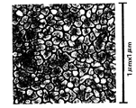
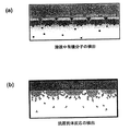
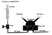
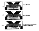
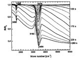
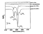
【解決手段】以下のステップ(ア)から(ウ)を設けた表面増強赤外吸収センサーの製造方法。(ア)溶液中に分散した金属ナノ粒子を誘電体基板表面に吸着させる。(イ)吸着した金属ナノ粒子を溶液中で成長させることにより、誘電体基板表面に、扁平且つ互いに分断され島状に配置された複数の金属ナノ薄膜を製膜する。(ウ)ステップ(イ)を行っている間、基板の金属ナノ薄膜が配置されている側とは反対側の面から赤外光を照射し、基板から染み出したエバネッセント波を用いて複数の金属ナノ薄膜の赤外吸収シグナルをその場モニターして吸収スペクトルの変化を評価することにより、複数の金属薄膜が十分に扁平に成長して、しかも金属ナノ薄膜同士が繋がり始め系全体が導電性を発現する直前に成長を停止する。
【選択図】図3
Description
M. Osawa, Bull. Chem. Soc. Jpn. 70, 2681-2880(1997) D. Enders, T. Nagao, T. Nakayama, and M .Aono, Langmuir 23, 6119(2007) D. Enders, T. Nagao, A. Pucci and T. Nakayama Surf. Sci., 600, L71 (2006) D. Enders, T. Nagao, and T. Nakayama Jpn. J. Appl. Phys. 46, 3020 (2007)
(ア)溶液中に分散した金属ナノ粒子を誘電体基板表面に吸着させる。
(イ)前記吸着した金属ナノ粒子を溶液中で成長させることにより、前記誘電体基板表面に、扁平且つ互いに分断され島状に配置された複数の金属ナノ薄膜を製膜する。
(ウ)前記ステップ(イ)を行っている間、前記基板の金属ナノ薄膜が配置されている側とは反対側の面から赤外光を照射し、前記基板から染み出したエバネッセント波を用いて前記複数の金属ナノ薄膜の赤外吸収シグナルをその場モニターして吸収スペクトルの変化を評価することにより、前記複数の金属薄膜が十分に扁平に成長して、しかも前記金属ナノ薄膜同士が繋がり始め系全体が導電性を発現する直前に前記成長を停止する。
第3に、上記第1または第2の発明において、前記複数の金属ナノ薄膜の前記基板上における2次元充填率が0.7以上1未満である表面増強赤外吸収センサーの製造方法を、
第4に、上記第1から第3の何れかの発明において、前記複数の金属薄膜の大きさが200nm以下である表面増強赤外吸収センサーの製造方法を、
第5に、上記第4の発明において、前記複数の金属薄膜の大きさが50nm以上である表面増強赤外吸収センサーの製造方法を、
第6に、上記第1から第5の何れかの発明において、前記複数の金属ナノ薄膜の隣接するもの同士の平均間隔が7nm以下である表面増強赤外吸収センサーの製造方法を、
第7に、上記第6の発明において、前記平均間隔が3nm以上である表面増強赤外吸収センサーの製造方法を、
第8に、上記第1から第7の何れかの発明において、前記複数の金属薄膜の幅と厚さの比が0.2以下である表面増強赤外吸収センサーの製造方法を、
第9に、上記第1から第8の何れかの発明において、前記赤外線の照射によるモニターを全反射減衰法で行う表面増強赤外吸収センサーの製造方法を、
提供する。
(ア)溶液中に分散した金属ナノ粒子を誘電体基板表面に吸着させる。
(イ)前記吸着した金属ナノ粒子を溶液中で成長させることにより、前記誘電体基板表面に、扁平且つ互いに分断され島状に配置された複数の金属ナノ薄膜を製膜する。
(ウ)前記ステップ(イ)を行っている間、前記基板の金属ナノ薄膜が配置されている側とは反対側の面から赤外光を照射し、前記基板から染み出したエバネッセント波を用いて前記複数の金属ナノ薄膜の赤外吸収シグナルをその場モニターして吸収スペクトルの変化を評価することにより、前記複数の金属薄膜が十分に扁平に成長して、しかも前記金属ナノ薄膜同士が繋がり始め系全体が導電性を発現する直前に前記成長を停止する。

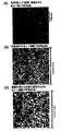
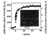
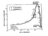
ここで、指数αの値が1の場合は通常(ガス吸着などの場合)のLangumuirキネティクスであり、α=1/2の場合は拡散に律速された拡張Langmuirモデルの場合に相当することが知られている。図9の灰色のカーブがベストフィットの結果であるが、実験と計算の結果は驚くほど一致している。実験は数回行い、その結果に対して得たフィッティングパラメータの値は、ckL=0.134、α=0.39−0.42となった。ここで得られたαの値は拡張Langmuirモデルに非常に近い値である。つまりAu粒子が表面まで届くレートは、溶液中のAu粒子のブラウン運動で律速される。一度界面に到着し吸着したAu粒子は固定化されて、同じ場所への粒子の吸着をブロックすることを示している。これは、先に述べたようにAuナノ粒子がマイナスに帯電した粒子であり、粒子同士は斥力で反発しあうことを考えると、良く理解できる。ここで扱う吸着粒子は、通常の原子や分子ではなく、重い金属原子数万個からなり、クエン酸分子で覆われ帯電した巨大な複合体である。また、吸着サイトも特定サイトがあるわけではなくSEM像からわかるように全くランダムに吸着している。
Claims (9)
- 以下のステップ(ア)から(ウ)を設けた表面増強赤外吸収センサーの製造方法。
(ア)溶液中に分散した金属ナノ粒子を誘電体基板表面に吸着させる。
(イ)前記吸着した金属ナノ粒子を溶液中で成長させることにより、前記誘電体基板表面に、扁平且つ互いに分断され島状に配置された複数の金属ナノ薄膜を製膜する。
(ウ)前記ステップ(イ)を行っている間、前記基板の金属ナノ薄膜が配置されている側とは反対側の面から赤外光を照射し、前記基板から染み出したエバネッセント波を用いて前記複数の金属ナノ薄膜の赤外吸収シグナルをその場モニターして吸収スペクトルの変化を評価することにより、前記複数の金属薄膜が十分に扁平に成長して、しかも前記金属ナノ薄膜同士が繋がり始め系全体が導電性を発現する直前に前記成長を停止する。 - 前記吸収スペクトルの変化は前記吸収スペクトの形状の変化である、請求項1に記載の表面増強赤外吸収センサーの製造方法。
- 前記複数の金属ナノ薄膜の前記基板上における2次元充填率が0.7以上1未満である、請求項1または2に記載の表面増強赤外吸収センサーの製造方法。
- 前記複数の金属薄膜の大きさが200nm以下である、請求項1から3の何れかに記載の表面増強赤外吸収センサーの製造方法。
- 前記複数の金属薄膜の大きさが50nm以上である、請求項4に記載の表面増強赤外吸収センサーの製造方法。
- 前記複数の金属ナノ薄膜の隣接するもの同士の平均間隔が7nm以下である、請求項1から5の何れかに記載の表面増強赤外吸収センサーの製造方法。
- 前記平均間隔が3nm以上である、請求項6に記載の表面増強赤外吸収センサーの製造方法。
- 前記複数の金属薄膜の幅と厚さの比が0.2以下である、請求項1から7の何れかに記載の表面増強赤外吸収センサーの製造方法。
- 前記赤外線の照射によるモニターを全反射減衰法で行う、請求項1から8の何れかに記載の表面増強赤外吸収センサーの製造方法。
Priority Applications (1)
| Application Number | Priority Date | Filing Date | Title |
|---|---|---|---|
| JP2012144529A JP5476574B2 (ja) | 2007-09-07 | 2012-06-27 | 表面増強赤外吸収センサーの製造方法 |
Applications Claiming Priority (3)
| Application Number | Priority Date | Filing Date | Title |
|---|---|---|---|
| JP2007233049 | 2007-09-07 | ||
| JP2007233049 | 2007-09-07 | ||
| JP2012144529A JP5476574B2 (ja) | 2007-09-07 | 2012-06-27 | 表面増強赤外吸収センサーの製造方法 |
Related Parent Applications (1)
| Application Number | Title | Priority Date | Filing Date |
|---|---|---|---|
| JP2008228904A Division JP5408565B2 (ja) | 2007-09-07 | 2008-09-05 | 表面増強赤外吸収センサー材料 |
Publications (2)
| Publication Number | Publication Date |
|---|---|
| JP2012233903A true JP2012233903A (ja) | 2012-11-29 |
| JP5476574B2 JP5476574B2 (ja) | 2014-04-23 |
Family
ID=40428974
Family Applications (2)
| Application Number | Title | Priority Date | Filing Date |
|---|---|---|---|
| JP2008228904A Expired - Fee Related JP5408565B2 (ja) | 2007-09-07 | 2008-09-05 | 表面増強赤外吸収センサー材料 |
| JP2012144529A Expired - Fee Related JP5476574B2 (ja) | 2007-09-07 | 2012-06-27 | 表面増強赤外吸収センサーの製造方法 |
Family Applications Before (1)
| Application Number | Title | Priority Date | Filing Date |
|---|---|---|---|
| JP2008228904A Expired - Fee Related JP5408565B2 (ja) | 2007-09-07 | 2008-09-05 | 表面増強赤外吸収センサー材料 |
Country Status (4)
| Country | Link |
|---|---|
| US (1) | US8193499B2 (ja) |
| EP (1) | EP2199777A4 (ja) |
| JP (2) | JP5408565B2 (ja) |
| WO (1) | WO2009031662A1 (ja) |
Families Citing this family (23)
| Publication number | Priority date | Publication date | Assignee | Title |
|---|---|---|---|---|
| WO2011050165A2 (en) * | 2009-10-21 | 2011-04-28 | Stc.Unm | Plasmonic detectors |
| JP5971789B2 (ja) * | 2010-08-31 | 2016-08-17 | 国立研究開発法人物質・材料研究機構 | ファイバー用プローブの作製方法 |
| JP5604334B2 (ja) * | 2011-02-28 | 2014-10-08 | 出光興産株式会社 | 吸着性化合物の分析方法 |
| DE102012004582B4 (de) | 2012-03-09 | 2014-02-20 | Fraunhofer-Gesellschaft zur Förderung der angewandten Forschung e.V. | Sensorsubstrat für die oberflächenverstärkte Spektroskopie |
| CN102621093A (zh) * | 2012-03-31 | 2012-08-01 | 上海大学 | 光谱研究金属及合金之缓蚀剂的作用及其择优化表面技术 |
| JP6146898B2 (ja) | 2012-06-29 | 2017-06-14 | 国立研究開発法人物質・材料研究機構 | 表面増強ラマン分光分析用(sers)基板、その製造方法、それを用いたバイオセンサおよびそれを用いたマイクロ流路デバイス |
| JP6124327B2 (ja) * | 2012-11-26 | 2017-05-10 | 国立研究開発法人物質・材料研究機構 | 金属検出センサー並びに金属検出方法及び装置 |
| JP6396012B2 (ja) * | 2013-10-31 | 2018-09-26 | 富士電機株式会社 | 光増強素子 |
| KR20150054179A (ko) | 2013-11-11 | 2015-05-20 | 삼성전자주식회사 | 레이저 유도 초음파 발생장치 및 그 제조방법 |
| US9823188B1 (en) * | 2014-09-09 | 2017-11-21 | University Of South Florida | Systems and methods for detecting the presence of a contaminant |
| CN104707992A (zh) * | 2014-12-01 | 2015-06-17 | 中国科学院合肥物质科学研究院 | 一种超结构Au/Ag@Al2O3@Ag纳米球阵列的制备方法及其SERS性能 |
| US10627335B2 (en) | 2015-07-13 | 2020-04-21 | Riken | Structure for use in infrared spectroscopy and infrared spectroscopy method using same |
| EP3365861A4 (en) | 2015-10-19 | 2019-04-24 | Merit Medical Systems, Inc. | SYSTEMS AND METHOD FOR PRODUCING MEDICAL DEVICES |
| US11125693B2 (en) * | 2017-01-31 | 2021-09-21 | Hewlett-Packard Development Company, L.P. | Surface enhanced infrared absorption stage |
| CN108254353B (zh) * | 2017-12-29 | 2019-04-16 | 重庆大学 | 石墨烯金属共形纳米探针增强拉曼红外双光谱器件及制备方法 |
| CN111060469A (zh) * | 2019-12-31 | 2020-04-24 | 深圳大学 | 一种生物检测芯片、生物传感器及其制备方法、用途 |
| CN111929225B (zh) * | 2020-08-19 | 2022-03-01 | 中国科学技术大学 | 分析污染物与单颗粒相互作用的装置及方法 |
| US12113279B2 (en) | 2020-09-22 | 2024-10-08 | Oti Lumionics Inc. | Device incorporating an IR signal transmissive region |
| KR20230106602A (ko) * | 2020-10-09 | 2023-07-13 | 오티아이 루미오닉스 인크. | 낮은 지수 코팅 및 방사선 수정 층을 포함하는 디바이스 |
| US11985841B2 (en) | 2020-12-07 | 2024-05-14 | Oti Lumionics Inc. | Patterning a conductive deposited layer using a nucleation inhibiting coating and an underlying metallic coating |
| CN113418886B (zh) * | 2021-06-18 | 2022-09-23 | 北京航空航天大学 | 一种表面增强红外光谱吸收信号的金纳米结构和方法 |
| CN114216876B (zh) * | 2021-08-23 | 2023-08-11 | 南开大学 | 一种表面增强红外基底制备及纳米柱阵列偏离角检测方法 |
| CN119715440B (zh) * | 2024-12-02 | 2026-01-09 | 厦门大学 | 一种超薄金微纳米结构的中红外分子传感器及其制备方法 |
Citations (2)
| Publication number | Priority date | Publication date | Assignee | Title |
|---|---|---|---|---|
| JPH0862125A (ja) * | 1994-08-22 | 1996-03-08 | Nissin Electric Co Ltd | 全反射分光法による基板表面処理評価方法及び装置 |
| JP2002267602A (ja) * | 2001-03-13 | 2002-09-18 | Konica Corp | 表面増強赤外吸収分光用島状金属膜材料及びその製造方法 |
Family Cites Families (5)
| Publication number | Priority date | Publication date | Assignee | Title |
|---|---|---|---|---|
| JP2003014765A (ja) * | 2001-07-02 | 2003-01-15 | Inst Of Physical & Chemical Res | センサーおよびそれを用いた物質の反応の検出方法 |
| JP3837508B2 (ja) * | 2002-06-14 | 2006-10-25 | 独立行政法人産業技術総合研究所 | 表面プラズモン励起性貴金属微粒子状薄膜 |
| JP2006208057A (ja) * | 2005-01-25 | 2006-08-10 | Taiyo Yuden Co Ltd | プラズモン共鳴構造体,その制御方法,金属ドメイン製造方法 |
| JP4947253B2 (ja) * | 2005-06-16 | 2012-06-06 | 隆雄 齋藤 | プラズモン共鳴構造体及びその製造方法 |
| JP2007078488A (ja) * | 2005-09-13 | 2007-03-29 | Hokkaido Univ | 電気化学赤外分光装置 |
-
2008
- 2008-09-05 JP JP2008228904A patent/JP5408565B2/ja not_active Expired - Fee Related
- 2008-09-05 US US12/676,723 patent/US8193499B2/en not_active Expired - Fee Related
- 2008-09-05 WO PCT/JP2008/066107 patent/WO2009031662A1/ja not_active Ceased
- 2008-09-05 EP EP08828985.5A patent/EP2199777A4/en not_active Withdrawn
-
2012
- 2012-06-27 JP JP2012144529A patent/JP5476574B2/ja not_active Expired - Fee Related
Patent Citations (2)
| Publication number | Priority date | Publication date | Assignee | Title |
|---|---|---|---|---|
| JPH0862125A (ja) * | 1994-08-22 | 1996-03-08 | Nissin Electric Co Ltd | 全反射分光法による基板表面処理評価方法及び装置 |
| JP2002267602A (ja) * | 2001-03-13 | 2002-09-18 | Konica Corp | 表面増強赤外吸収分光用島状金属膜材料及びその製造方法 |
Also Published As
| Publication number | Publication date |
|---|---|
| JP5476574B2 (ja) | 2014-04-23 |
| US20100239821A1 (en) | 2010-09-23 |
| EP2199777A4 (en) | 2013-06-19 |
| US8193499B2 (en) | 2012-06-05 |
| JP5408565B2 (ja) | 2014-02-05 |
| JP2009080109A (ja) | 2009-04-16 |
| WO2009031662A1 (ja) | 2009-03-12 |
| EP2199777A1 (en) | 2010-06-23 |
Similar Documents
| Publication | Publication Date | Title |
|---|---|---|
| JP5476574B2 (ja) | 表面増強赤外吸収センサーの製造方法 | |
| Peng et al. | Charge-transfer resonance and electromagnetic enhancement synergistically enabling MXenes with excellent SERS sensitivity for SARS-CoV-2 S protein detection | |
| Lin et al. | Surface-enhanced Raman spectroscopy: substrate-related issues | |
| Enders et al. | Surface-enhanced ATR-IR spectroscopy with interface-grown plasmonic gold-island films near the percolation threshold | |
| Huo et al. | Seeded-growth approach to fabrication of silver nanoparticle films on silicon for electrochemical ATR surface-enhanced IR absorption spectroscopy | |
| Yang et al. | Ultraviolet–visible plasmonic properties of gallium nanoparticles investigated by variable-angle spectroscopic and Mueller matrix ellipsometry | |
| JP6420899B2 (ja) | 分光センサおよびその製造方法 | |
| TWI404930B (zh) | Biochemical sensing wafer substrate and its preparation method | |
| CN103168001B (zh) | 金属络合物量子晶体的制造方法 | |
| CN108709879B (zh) | 基于介电高弹聚合物的表面增强拉曼散射活性薄膜及方法 | |
| Pal et al. | Ultra-sensitive, reusable, and superhydrophobic Ag/ZnO/Ag 3D hybrid surface enhanced Raman scattering substrate for hemoglobin detection | |
| Griffiths | Surface‐enhanced infrared absorption spectroscopy: principles and applications | |
| Guo et al. | Nafion stabilized Ag nanopillar arrays as a flexible SERS substrate for trace chemical detection | |
| CN108226137A (zh) | 一种柔性、透明的二硫化钼@银颗粒/三维金字塔结构pmma sers基底的制备方法及应用 | |
| Heinig et al. | Aminopropylsilatrane linkers for easy and fast fabrication of high-quality 10 nm thick gold films on SiO2 substrates | |
| Juntaracena et al. | Surface-enhanced Raman scattering activities and recyclability of Ag-incorporated WO3 nanofiber-based substrates | |
| Nowak et al. | Preparation and characterization of long-term stable SERS active materials as potential supports for medical diagnostic | |
| Shao et al. | Noble metal modified ReS2 nanocavity for surface-enhanced Raman spectroscopy (SERS) analysis | |
| Stoev et al. | Recent progresses in nanometer scale analysis of buried layers and interfaces in thin films by X-rays and Neutrons | |
| Fan et al. | Highly Sensitive SERS Detection of Food Additives Using Gold Nanospheres on Capillary Substrates | |
| JP5408576B2 (ja) | 近接場光源2次元アレイとその製造方法、2次元アレイ型表面プラズモン共振器、太陽電池、光センサー及びバイオセンサー | |
| CN113203726A (zh) | 一种用于雾霾颗粒物中芴的快速检测的表面增强拉曼基底的制备方法 | |
| JP5971789B2 (ja) | ファイバー用プローブの作製方法 | |
| Yang et al. | Enhanced photoelectrochemical detection of alpha-fetoprotein using dipole image effect and lock-in amplification | |
| Zou et al. | Construction and surface enhanced Raman scattering activity of gold nanoparticles array on boron doped diamond film |
Legal Events
| Date | Code | Title | Description |
|---|---|---|---|
| A131 | Notification of reasons for refusal |
Free format text: JAPANESE INTERMEDIATE CODE: A131 Effective date: 20130820 |
|
| A521 | Written amendment |
Free format text: JAPANESE INTERMEDIATE CODE: A523 Effective date: 20131018 |
|
| TRDD | Decision of grant or rejection written | ||
| A01 | Written decision to grant a patent or to grant a registration (utility model) |
Free format text: JAPANESE INTERMEDIATE CODE: A01 Effective date: 20140107 |
|
| A61 | First payment of annual fees (during grant procedure) |
Free format text: JAPANESE INTERMEDIATE CODE: A61 Effective date: 20140116 |
|
| R150 | Certificate of patent or registration of utility model |
Ref document number: 5476574 Country of ref document: JP Free format text: JAPANESE INTERMEDIATE CODE: R150 |
|
| S533 | Written request for registration of change of name |
Free format text: JAPANESE INTERMEDIATE CODE: R313533 |
|
| R350 | Written notification of registration of transfer |
Free format text: JAPANESE INTERMEDIATE CODE: R350 |
|
| R250 | Receipt of annual fees |
Free format text: JAPANESE INTERMEDIATE CODE: R250 |
|
| R250 | Receipt of annual fees |
Free format text: JAPANESE INTERMEDIATE CODE: R250 |
|
| R250 | Receipt of annual fees |
Free format text: JAPANESE INTERMEDIATE CODE: R250 |
|
| LAPS | Cancellation because of no payment of annual fees |