JP2012209537A - Lighting apparatus, display, and signal light - Google Patents
Lighting apparatus, display, and signal light Download PDFInfo
- Publication number
- JP2012209537A JP2012209537A JP2012018290A JP2012018290A JP2012209537A JP 2012209537 A JP2012209537 A JP 2012209537A JP 2012018290 A JP2012018290 A JP 2012018290A JP 2012018290 A JP2012018290 A JP 2012018290A JP 2012209537 A JP2012209537 A JP 2012209537A
- Authority
- JP
- Japan
- Prior art keywords
- support substrate
- light emitting
- emitting element
- light
- heat sinks
- Prior art date
- Legal status (The legal status is an assumption and is not a legal conclusion. Google has not performed a legal analysis and makes no representation as to the accuracy of the status listed.)
- Granted
Links
Images


Landscapes
- Led Device Packages (AREA)
- Liquid Crystal (AREA)
- Arrangement Of Elements, Cooling, Sealing, Or The Like Of Lighting Devices (AREA)
- Planar Illumination Modules (AREA)
Abstract
Description
本発明は、発光ダイオードを用いた照明装置、ディスプレイ、及び信号灯に関する。 The present invention relates to a lighting device, a display, and a signal lamp using a light emitting diode.
発光ダイオードを用いた発光デバイスは、省エネルギ、長寿命という利点があり、照明装置、カラー画像表示装置、液晶ディスプレイのバックライト、又は、交通信号灯などの光源として、注目されている。 A light emitting device using a light emitting diode has advantages such as energy saving and long life, and has attracted attention as a light source such as a lighting device, a color image display device, a liquid crystal display backlight, or a traffic light.
この種の発光デバイスについて、従来は、フリップ・チップ(FC)として構成されたLEDチップをサブマウント基板に実装し、更に、この組み立て体をパッケージング基板に実装し、サブマウント基板に形成された電極と、パッケージング基板に形成された電極とを、ワイヤ・ボンディングによって接続していた。 For this type of light emitting device, conventionally, an LED chip configured as a flip chip (FC) is mounted on a submount substrate, and this assembly is further mounted on a packaging substrate and formed on the submount substrate. The electrode and the electrode formed on the packaging substrate were connected by wire bonding.
しかし、この組み立て構造では、AlN等の高価な材料で構成されたサブマウント基板を使用しなければならいことから、コスト高になる。しかも、サブマウント基板に形成された電極と、パッケージング基板に形成された電極とを、ワイヤ・ボンディングによって接続する必要があるため、ワイヤボンダ装置・ワイヤボンディング装置が必要であり、生産設備費が増大し、それが製品コストに転嫁され、発光デバイスのコスト高を招いていた。 However, this assembly structure increases the cost because a submount substrate made of an expensive material such as AlN must be used. In addition, since the electrodes formed on the submount substrate and the electrodes formed on the packaging substrate must be connected by wire bonding, a wire bonder device and a wire bonding device are required, which increases production equipment costs. However, this has been passed on to the product cost, leading to high costs for light emitting devices.
上述した問題点を解決する手段として、特許文献1には、シリコン・サブマウントの一面に溝を形成し、その溝底部に2つのビア(貫通電極)を形成し、LEDダイスを、溝内にフリップ・チップ・マウントし、保護接着剤で溝を充填するLEDパッケージの製造方法が開示されている。
As means for solving the above-described problems,
しかしながら、LEDダイスの発光動作時に発生した熱を逃がす放熱構造については、全く考慮されていない。一般的に、LED装置は、低消費電力であるが、赤外放射が無い分を熱エネルギとして放出する点、発光素子が固体で覆われているために、放熱性が固体の熱伝導率に依存する点、並びにLED部品の表面積が小さいから、十分な熱の伝導面積、対流面積、及び放射面積が得られず、さらに従来のヒートシンクなどの放熱部品が取り付けられない点から、放熱設計が困難であるといわれている。 However, no consideration is given to a heat dissipation structure that releases heat generated during the light emitting operation of the LED die. In general, LED devices have low power consumption, but the amount of no infrared radiation is emitted as thermal energy, and since the light emitting elements are covered with solids, the heat dissipation becomes solid thermal conductivity. Because the surface area of the LED component is small and the surface area of the LED component is small, sufficient heat conduction area, convection area, and radiation area cannot be obtained, and furthermore, heat dissipation components such as conventional heat sinks cannot be attached, making it difficult to design heat dissipation It is said that it is.
したがって、複数のLEDを搭載する必要がある照明装置などに、上記のLEDパッケージのような十分な放熱構造がないものを適用すると、LEDダイスに発生した熱によって、LEDダイスとビアとを接続する接合部分の接合強度が失われ、電気的接続の信頼性が損なわれたり、あるいは、LEDダイスの発光特性が変動してしまうという問題を生じ得る。この点、特許文献2及び3には、発光装置で発生した熱を逃す構造としてサーマルビアを採用しているが、貫通電極を想定した放熱構造とはなっていない。
Accordingly, when a lighting device that needs to have a plurality of LEDs mounted thereon and that does not have a sufficient heat dissipation structure such as the LED package described above, the LED die and the via are connected by the heat generated in the LED die. The bonding strength of the bonding portion may be lost, and the reliability of electrical connection may be impaired, or the light emission characteristics of the LED die may vary. In this regard,
また、特許文献1に示されているように、ビア(貫通電極)を、電気メッキ又は蒸着によって形成する場合、処理時間がどうしても長くなるから、製造効率が悪くなる。このような問題を回避する手段として、ビアを、スルーホールに対する導電性ペースト埋め込み処理により形成することも考えられるが、スルーホール内に埋め込みした導電性ペーストが、凝固時に必ず収縮し、引け巣が生じることとなる。このような引け巣は、電気抵抗の増大、及び、信頼性低下等の原因となる。
Further, as shown in
更に、LEDダイスに発生した光を、効率よく外部に放射させるための手段が必要であるところ、特許文献1には、そのような手段が開示されていない。
Further, there is a need for means for efficiently radiating the light generated in the LED die to the outside, but
本発明の課題は、放熱特性を向上し得る照明装置、ディスプレイ、及び信号灯を提供することである。 The subject of this invention is providing the illuminating device, display, and signal lamp which can improve a thermal radiation characteristic.
上述した課題を解決するため、本発明に係る照明装置は、支持基板と、複数の発光素子とを含む。前記支持基板は、板面に複数の発光素子設置領域が設けられ、複数の貫通電極と、複数の柱状ヒートシンクとを含んでいる。 In order to solve the above-described problem, an illumination device according to the present invention includes a support substrate and a plurality of light emitting elements. The support substrate is provided with a plurality of light emitting element installation regions on the plate surface, and includes a plurality of through electrodes and a plurality of columnar heat sinks.
前記複数の貫通電極は、前記支持基板を厚み方向に貫通し、前記複数の発光素子設置領域のそれぞれに、一端が露出するように2個ずつ配置されている。また、前記複数の柱状ヒートシンクは、前記支持基板の厚み方向に設けられている。 The plurality of through-electrodes are arranged two by two so as to penetrate the support substrate in the thickness direction and to have one end exposed in each of the plurality of light-emitting element installation regions. The plurality of columnar heat sinks are provided in the thickness direction of the support substrate.
前記複数の発光素子は、それぞれ、P型半導体層及びN型半導体層を積層した構造を含み、前記支持基板の発光素子設置領域に配置され、前記P型半導体層のP側電極が、前記貫通電極の一方の前記一端に接続され、前記N型半導体層のN側電極が、前記貫通電極の他方の前記一端に接続されている。前記支持基板は、シリコン層を含み、前記複数の柱状ヒートシンクは、前記シリコン層を貫通し、互いに間隔を隔てて、前記発光素子の周囲に多数配置されており、前記支持基板との間に設けられた電気絶縁層によって前記支持基板から電気絶縁されており、前記複数の柱状ヒートシンクのそれぞれの一端は、前記支持基板の他面に設けられた放熱体に共通に接続されている。 Each of the plurality of light-emitting elements includes a structure in which a P-type semiconductor layer and an N-type semiconductor layer are stacked, and is disposed in a light-emitting element installation region of the support substrate, and a P-side electrode of the P-type semiconductor layer passes through the through-hole. The one end of the electrode is connected to the one end, and the N-side electrode of the N-type semiconductor layer is connected to the other end of the through electrode. The support substrate includes a silicon layer, and the plurality of columnar heat sinks are arranged around the light emitting element so as to penetrate the silicon layer and are spaced apart from each other, and are provided between the support substrate and the support substrate. The electrically insulating layer is electrically insulated from the support substrate, and one end of each of the plurality of columnar heat sinks is commonly connected to a heat radiator provided on the other surface of the support substrate.
上述したように、本発明に係る照明装置は、支持基板を含んでおり、この支持基板は、複数の柱状ヒートシンクを含んでいる。柱状ヒートシンクは、支持基板の厚み方向に設けられているため、発光素子の発光動作によって生じた熱を、柱状ヒートシンクによって、支持基板の外部に放熱することができる。 As described above, the lighting device according to the present invention includes a support substrate, and the support substrate includes a plurality of columnar heat sinks. Since the columnar heat sink is provided in the thickness direction of the support substrate, heat generated by the light emitting operation of the light emitting element can be radiated to the outside of the support substrate by the columnar heat sink.
柱状ヒートシンクは、支持基板の板面に対して所定の面積占有率をもって分布している。したがって、柱状ヒートシンクを構成する材料の熱抵抗、及び、柱状ヒートシンクの占有率を適切に選ぶことにより、発光素子の発光動作によって生じた熱を、柱状ヒートシンクによって、支持基板の外部に効率よく放熱しえる。 The columnar heat sink is distributed with a predetermined area occupancy with respect to the plate surface of the support substrate. Therefore, by appropriately selecting the thermal resistance of the material constituting the columnar heat sink and the occupation ratio of the columnar heat sink, the heat generated by the light emitting operation of the light emitting element is efficiently radiated to the outside of the support substrate by the column heat sink. Yeah.
本発明に係る照明装置において、支持基板は、複数の貫通電極を含み、板面に複数の発光素子設置領域を有している。貫通電極は、支持基板を厚み方向に貫通し、複数の発光素子設置領域のそれぞれに、一端が露出するように2個ずつ配置されている。この支持基板の発光素子設置領域に発光素子が配置されている。 In the lighting device according to the present invention, the support substrate includes a plurality of through electrodes and has a plurality of light emitting element installation regions on the plate surface. Two through-electrodes are arranged through the support substrate in the thickness direction, and two each of the through-electrodes are exposed in each of the plurality of light emitting element installation regions. A light emitting element is disposed in the light emitting element installation region of the support substrate.
発光素子は、P型半導体層及びN型半導体層を積層した構造である。そして、発光素子設置領域で、P型半導体層のP側電極が貫通電極の一方の一端に接続され、N型半導体層のN側電極が、貫通電極の他方の一端に接続されている。したがって、本発明によれば、発光素子の電極が、光出射面に現れない構造が実現できるから、発光素子の光を効率よく外部に放射させ得る。 The light emitting element has a structure in which a P-type semiconductor layer and an N-type semiconductor layer are stacked. In the light emitting element installation region, the P-side electrode of the P-type semiconductor layer is connected to one end of the through electrode, and the N-side electrode of the N-type semiconductor layer is connected to the other end of the through electrode. Therefore, according to the present invention, it is possible to realize a structure in which the electrode of the light emitting element does not appear on the light emitting surface, so that the light of the light emitting element can be efficiently emitted to the outside.
また、本発明に係る液晶ディスプレイは、液晶パネルと、バックライトとを含む。前記バックライトは、上述した照明装置であり、前記液晶パネルを背面から照明する。 The liquid crystal display according to the present invention includes a liquid crystal panel and a backlight. The backlight is the illumination device described above, and illuminates the liquid crystal panel from the back.
本発明に係る液晶ディスプレイは、上述した照明装置を含むから、既に述べた作用効果を奏する。 Since the liquid crystal display according to the present invention includes the above-described illumination device, the above-described effects can be obtained.
本発明の技術的思想の適用範囲は、上記の照明装置、及び液晶ディスプレイに限られない。 The scope of application of the technical idea of the present invention is not limited to the illumination device and the liquid crystal display.
本発明に係る発光ダイオードディスプレイは、支持基板と、複数の発光素子とを含む。前記支持基板は、板面に複数の発光素子設置領域が設けられ、複数の貫通電極と、複数の柱状ヒートシンクとを含んでいる。 The light emitting diode display according to the present invention includes a support substrate and a plurality of light emitting elements. The support substrate is provided with a plurality of light emitting element installation regions on the plate surface, and includes a plurality of through electrodes and a plurality of columnar heat sinks.
前記複数の貫通電極は、前記支持基板を厚み方向に貫通し、前記複数の発光素子設置領域のそれぞれに、一端が露出するように2個ずつ配置されている。また、前記複数の柱状ヒートシンクは、前記支持基板の厚み方向に設けられ、前記板面に対して所定の面積占有率をもって分布している。 The plurality of through-electrodes are arranged two by two so as to penetrate the support substrate in the thickness direction and to have one end exposed in each of the plurality of light-emitting element installation regions. The plurality of columnar heat sinks are provided in the thickness direction of the support substrate and are distributed with a predetermined area occupancy with respect to the plate surface.
前記複数の発光素子は、それぞれ、P型半導体層及びN型半導体層を積層した構造を含み、前記支持基板の前記発光素子設置領域に配置され、前記P型半導体層のP側電極が、前記貫通電極の一方の前記一端に接続され、前記N型半導体層のN側電極が、前記貫通電極の他方の前記一端に接続されている。 Each of the plurality of light-emitting elements includes a structure in which a P-type semiconductor layer and an N-type semiconductor layer are stacked, and is disposed in the light-emitting element installation region of the support substrate, and a P-side electrode of the P-type semiconductor layer is One end of the through electrode is connected to the one end, and the N-side electrode of the N-type semiconductor layer is connected to the other end of the through electrode.
更に、前記支持基板は、シリコン層を含み、前記複数の柱状ヒートシンクは、前記シリコン層を貫通し、互いに間隔を隔てて、前記発光素子の周囲に多数配置されており、前記支持基板との間に設けられた電気絶縁層によって前記支持基板から電気絶縁されており、前記複数の柱状ヒートシンクのそれぞれの一端は、前記支持基板の他面に設けられた放熱体に共通に接続されている。 Further, the support substrate includes a silicon layer, and the plurality of columnar heat sinks are arranged around the light emitting element so as to penetrate the silicon layer and are spaced apart from each other. The insulating substrate is electrically insulated from the support substrate, and one end of each of the plurality of columnar heat sinks is commonly connected to a heat radiator provided on the other surface of the support substrate.
本発明に係る発光ダイオードディスプレイは、上述した照明装置と同様の構成を含むから、既に述べた作用効果を奏する。 Since the light-emitting diode display according to the present invention includes the same configuration as that of the above-described lighting device, the above-described effects can be obtained.
さらに、本発明に係る信号灯は、支持基板と、複数の発光素子とを含む。前記支持基板は、板面に複数の発光素子設置領域が設けられ、複数の貫通電極と、複数の柱状ヒートシンクとを含んでいる。 Furthermore, the signal lamp according to the present invention includes a support substrate and a plurality of light emitting elements. The support substrate is provided with a plurality of light emitting element installation regions on the plate surface, and includes a plurality of through electrodes and a plurality of columnar heat sinks.
前記複数の貫通電極は、前記支持基板を厚み方向に貫通し、前記複数の発光素子設置領域のそれぞれに、一端が露出するように2個ずつ配置されている。また、前記複数の柱状ヒートシンクは、前記支持基板の厚み方向に設けられ、前記板面に対して所定の面積占有率をもって分布している。 The plurality of through-electrodes are arranged two by two so as to penetrate the support substrate in the thickness direction and to have one end exposed in each of the plurality of light-emitting element installation regions. The plurality of columnar heat sinks are provided in the thickness direction of the support substrate and are distributed with a predetermined area occupancy with respect to the plate surface.
前記複数の発光素子は、それぞれ、P型半導体層及びN型半導体層を積層した構造を含み、前記支持基板の発光素子設置領域に配置され、前記P型半導体層のP側電極が、前記貫通電極の一方の前記一端に接続され、前記N型半導体層のN側電極が、前記貫通電極の他方の前記一端に接続されている。 Each of the plurality of light-emitting elements includes a structure in which a P-type semiconductor layer and an N-type semiconductor layer are stacked, and is disposed in a light-emitting element installation region of the support substrate, and a P-side electrode of the P-type semiconductor layer passes through the through-hole. The one end of the electrode is connected to the one end, and the N-side electrode of the N-type semiconductor layer is connected to the other end of the through electrode.
更に、前記支持基板は、シリコン層を含み、前記複数の柱状ヒートシンクは、前記シリコン層を貫通し、互いに間隔を隔てて、前記発光素子の周囲に多数配置されており、前記支持基板との間に設けられた電気絶縁層によって前記支持基板から電気絶縁されており、前記複数の柱状ヒートシンクのそれぞれの一端は、前記支持基板の他面に設けられた放熱体に共通に接続されている。 Further, the support substrate includes a silicon layer, and the plurality of columnar heat sinks are arranged around the light emitting element so as to penetrate the silicon layer and are spaced apart from each other. The insulating substrate is electrically insulated from the support substrate, and one end of each of the plurality of columnar heat sinks is commonly connected to a heat radiator provided on the other surface of the support substrate.
本発明に係る信号灯は、上述した照明装置と同様の構成を含むから、既に述べた作用効果を奏する。 Since the signal lamp according to the present invention includes the same configuration as that of the lighting device described above, the above-described effects can be obtained.
以上述べたように、本発明によれば、放熱特性を向上し得る照明装置、ディスプレイ、及び信号灯を提供することができる。 As described above, according to the present invention, it is possible to provide an illumination device, a display, and a signal lamp that can improve heat dissipation characteristics.
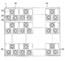
図1は、本発明に係る照明装置の平面図である。本発明に係る照明装置は、矩形状の支持基板1と、この支持基板1にマトリックス状に配列された複数の発光デバイス2とを含む。
FIG. 1 is a plan view of a lighting device according to the present invention. The illumination device according to the present invention includes a
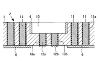
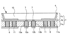
各発光デバイス2は、所定の色相の光を発する発光素子3と、発光素子3を電気的に接続するための2個の貫通電極12a,12bと、放熱のために発光素子3の周囲に配置された複数の柱状ヒートシンク11とを有する。各発光素子3は、支持基板1の板面に形成された発光素子設置領域となる凹部10内に設けられている。なお、支持基板1の形状、発光デバイス2の数、及び、配置形態、並びに柱状ヒートシンク11の数、及び配置形態は、図1に示された形態に限られず、適宜に決定すべきものである。
Each
図2〜図4には上記の発光デバイス2が詳細に示されている。支持基板1は、いわゆるパッケージとなるものであって、複数の貫通電極12a,12bと、複数の柱状ヒートシンク11とを含み、板面に凹部10を有している。支持基板1は、Siを主成分とするものを採用すると好適であるが、これに限られず、絶縁樹脂基板、又は絶縁性セラミック基板を採用してもよい。更には、金属基板等の導電性基板であってもよい。本実施形態では、支持基板1がシリコン層の場合を例にとって説明する。
2 to 4 show the
支持基板1の凹部10の形状は、図4に示されるような直方体形状に限られることはなく、他の形状であってもよい。この凹部10は、支持基板1を平面視したときに、貫通電極12a,12bを、間隔をおいて囲むように形成されていて、その内側面のほぼ全周に、例えば、Al膜、Ag膜又はCr膜等でなる反射膜4がスパッタ等によって形成されている。反射膜4は、上述した形態に限定されず、例えば発光素子3の側面に付着されてもよく、また、反射膜4の下側に酸化膜等の絶縁膜を設けてもよい。
The shape of the
発光素子3は、凹部10に、微小なクリアランスをもって嵌めこまれている。この構造によれば、支持基板1に対する発光素子3の位置決め・配置を、容易、かつ、確実に実行することができる。
The
また、発光素子3は、凹部10内において、上面を蛍光層5により覆われている。これにより、発光素子3の発する光の輝度を向上することができる。蛍光層5に用いられる蛍光物質としては、例えばリン酸カルシウムがある。また、蛍光層5の色相は、用途に応じて適宜に決定すべきものである。
Further, the upper surface of the
貫通電極12a,12bのそれぞれは、凹部10の底面内において、支持基板1を厚み方向に貫通し、一端が凹部10の内面に露出し、他端が支持基板1の他面に露出する。貫通電極12a,12bは、中身の詰まった中実柱状体であって、角形状、円形状等、任意の断面形状をとることができる。また、貫通電極12a,12bの端面形状を、接続される発光素子3の電極形状と対応させてもよく、この場合、貫通電極12a,12bの端面形状は、それぞれ円形状と四角形状になる。
Each of the through
本実施形態における支持基板1は、シリコン層であるので、貫通電極12a、12bは支持基板1から電気絶縁されている。電気絶縁の手段として、貫通電極12a、12bの外周面と、貫通電極12a、12bが配置された縦孔の内周面との間に、電気絶縁層13a、13bが設けられている。電気絶縁層13a、13bは、シリコン層でなる支持基板1の縦孔内壁面を酸化または窒化して得られた酸化膜または窒化膜であってもよいし、縦孔内に充填された有機絶縁物またはガラス等の無機絶縁物から構成された層であってもよい。
Since the
貫通電極12a,12bは、例えば、凝固金属体でなる。凝固金属体を用いることの利点は、支持基板1に設けられた縦孔内に溶融金属を流し込み、凝固させる溶融金属充填法を適用できることである。溶融金属充填法は、特許第4278007号公報に開示されている。この溶融金属充填法を適用することにより、縦孔内に流し込まれた溶融金属に、機械的な力、例えばプレス板を用いたプレス圧、射出圧または転圧を印加しながら、冷却し、凝固させ、それによって、巣、空隙、空洞のない緻密な構造を持つ貫通電極12a,12bを、短時間で、効率よく形成することができる。
The through
貫通電極12a,12bを、溶融金属充填法を用いて形成する場合に用いられる金属材料の主なものとしては、Bi、In、Sn及びCuを例示することができる。特に、Biを含有させると、Biの持つ凝固時の体積膨張特性により、縦孔の内部で、空洞や空隙を生じることのない緻密な貫通電極12a,12bを形成することができる。もっとも、Bi等を含有させると、電気抵抗が増大する傾向にあるので、要求される電気抵抗値を満たす限度で、Biを使用することが好ましい。
Bi, In, Sn, and Cu can be exemplified as the main metal materials used when the through
溶融金属としては、上述した金属材料を用いて、粒径1μm以下の多結晶体の集合体でなるナノコンポジット結晶構造をもつナノ粒子の粉体を溶融したものを用いることができる。このように、大きさが、ナノレベルに制限されたナノ粒子を含むことにより、微細な縦孔内に溶融金属を充填して貫通電極12a,12bを形成することができる。ナノコンポジット結晶構造には、(a)非共晶組織の内部に共晶組織でなるナノ粒子を分散させたもの、(b)非共晶組織の粒界に共晶組織でなるナノ粒子を分散させたもの、(c)共晶組織の粒界に非共晶組織でなるナノ粒子を分散させたもの、(d)非共晶組織の内部に共晶組織でなるナノ粒子を分散させるとともに、非共晶組織の粒界に共晶組織でなるナノ粒子を分散させたもの、(e)共晶組織及び非共晶組織が、共にナノサイズであるものなどが含まれる。なお、ナノコンポジット結晶構造を有するナノ粒子を用いて形成した貫通電極12a,12bも、ナノコンポジット結晶構造となる。
As the molten metal, it is possible to use a material obtained by melting a nanoparticle powder having a nanocomposite crystal structure composed of an aggregate of polycrystals having a particle size of 1 μm or less using the above-described metal material. As described above, by including nanoparticles whose size is limited to the nano level, it is possible to form the through
さらに、溶融金属充填法の他に、上述した金属材料の金属微粉末を、液状分散媒に分散した液状分散系を、縦孔内に充填し、液状分散媒を蒸発させた後に、熱処理によって金属微粉末を熱溶解させ、加圧しながら硬化させる方法(液状分散系充填法)を採用することもできる。 Further, in addition to the molten metal filling method, the liquid dispersion system in which the metal fine powder of the above-described metal material is dispersed in the liquid dispersion medium is filled in the vertical holes, and after the liquid dispersion medium is evaporated, the metal is processed by heat treatment. It is also possible to employ a method (liquid dispersion filling method) in which fine powder is melted with heat and cured while being pressed.
柱状ヒートシンク11は、支持基板1の厚み方向に設けられ、板面に対して所定の面積占有率をもって分布している。柱状ヒートシンク11に適した材料は、熱抵抗の低い材料である。柱状ヒートシンク11も、貫通電極12a,12bと同様に、溶融金属充填法や液状分散系充填法を利用したナノコンポジット結晶構造を有する金属体で構成することができる。限定するものではないが、具体例として、Al、Cu又はZn等に、Sn、Ga又はIn等の低融点金属材料を添加したものを挙げることができる。もっとも、柱状ヒートシンク11は、熱抵抗ができるだけ小さいこと好ましいから、材料及び組成比等は、そのような視点から選定する必要がある。本実施形態では、柱状ヒートシンク11は、中身の詰まった中実柱状体であって、断面円形状であるが、角形状であってもよい。また、柱状ヒートシンク11についても、その周りを、電気絶縁層11aによって覆い、柱状ヒートシンク11を、シリコン層である支持基板1から電気的に絶縁される。
The
柱状ヒートシンク11は、支持基板1の厚み方向に貫通し、互いに微小間隔を隔てて、マトリクス状に多数配置され、支持基板1の裏面(他面)に設けられた放熱体6に接続されている。これにより、柱状ヒートシンク11は、基板1から効果的に熱を逃がすことができる。
The
支持基板1は、シリコン層であり、複数の柱状ヒートシンク11は、シリコン層を貫通し、互いに間隔を隔てて、発光素子3の周囲に多数配置されており、複数の柱状ヒートシンク11のそれぞれの一端及び前記シリコン層は、支持基板1の他面に設けられた放熱体6に共通に接続されている。この構造によれば、シリコン層の良好な放熱特性により、3次元的放熱経路が構成され、照明装置全体としての放熱特性を向上させることができる。即ち、発光素子3で発生した熱を、シリコン層によって集熱し、シリコン層から柱状ヒートシンク11に伝達し、更に柱状ヒートシンク11からシリコン層を介して、他のヒートシンク11に伝達し、ヒートシンク11から支持基板1の他面に設けられた放熱体6に伝達し、放熱体6から、支持基板1の面方向に向かって外部に拡散放出することができる。
The
放熱体6は、例えばアルミニウムなどの比較的に熱伝導率の高い物質からなり、支持基板1の裏面に、複数個に分けて設けてもよいし、あるいは、全てのヒートシンク3に対して共通に接続される単一の部材として設けてもよい。また、放熱体6の形態は、図示の膜状に限らず、拡大された放熱面積を有する3次元的構造であってもよい。
The
柱状ヒートシンク11の奏する放熱特性は、基本的には、その組成材料の持つ熱伝導率(又は熱抵抗)と、支持基板1の平面積に対して、柱状ヒートシンク11の全体が占める占有率とによって定まる。例えば、柱状ヒートシンク11として、熱抵抗の低い材料を用いた場合には、占有率を低下させ、熱抵抗の高い材料を用いた場合には、占有率を上げる。即ち、柱状ヒートシンク11の占有率は、その組成材料の熱伝導率を考慮して定めることになる。逆に、占有率に制限がある場合には、求められる放熱特性を考慮して、適合する熱伝導率の材料を選択することになる。
The heat dissipation characteristics of the
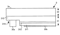
図4と図5には、発光素子3の詳細が示されている。発光素子3は、発光ダイオードであって、白色発光素子、赤色発光素子、緑色発光素子、青色発光素子、橙色発光素子の何れであってもよい。発光素子3の光出射面3aの高さ位置は、支持基板1の表面の高さ位置より低くなっており、蛍光層5は、その両者の段差を埋めるように充填されている。
4 and 5 show details of the light-emitting
発光素子3は、透明結晶層32と、P型半導体層311、及びN型半導体層313を積層した半導体積層構造31とを含んでいる。さらに、P型半導体層311、及びN型半導体層313の間には活性層312が設けられている。
The
透明結晶層32は、代表的にはサファイアであり、その一面が光出射面3aとなる。この光出射面3aに、微細凹凸形状を有する透明光学部品(図示せず)を配置した場合、光出射面3aで、光を拡散又は分散させ、均一な面発光を実現することができる。なお、該透明光学部品を設ける代わりに、光出射面3a自体に微細凹凸形状が形成されていてもよい。
The
一方、光出射面3aの反対面にはバッファ層(図示せず)があり、このバッファ層を介して、半導体積層構造31が透明結晶層32の上に成長させてある。半導体積層構造31は、典型的にはIII−V族化合物半導体であるが、これに限定されず、PN接合を有する他の化合物半導体も採用し得る。
On the other hand, a buffer layer (not shown) is provided on the surface opposite to the
透明結晶層32の側に位置するN型半導体層313は、P型半導体層311と重ならない部分314を有しており、N側電極30aが、その重ならない部分314の表面に設けられている。一方、P側電極30bは、重なる部分において、P型半導体層311の表面に設けられている。なお、N側電極30aは、円形状に限らず、角形状であってもよい。
The N-
本実施形態において、重ならない部分314に設けられたN側電極30aの平面積は、重なる部分に設けられたP側電極30bの平面積よりも小さい。より詳しくは、N側電極30a及びP側電極30bの配置方向で見た電極幅について、N側電極30aの電極幅がP側電極30bの電極幅よりも小さい。このような電極配置によれば、重ならない部分314の幅を小さくし、反射的に、発光領域となる重なる部分の幅及び面積を拡大できるから、発光量を増大することができる。
In the present embodiment, the plane area of the N-
発光素子3は、図2と図3に示されるように、凹部10内において、P型半導体層311のP側電極30bが一方の貫通電極12bの一端に接続され、N型半導体層313のN側電極30aが他方の貫通電極21aの一端に接続されている。P側電極30b、及びN側電極30aは、間隔を隔てて互いに対向している。P側電極30bと貫通電極12bとの接合、及び、N側電極30aと貫通電極12aとの接合にあたっては、両者の接合界面に接合膜を介在させる。接合膜は、Sn、In、Bi、Ga又はSbの群から選択された少なくても1種の低融点金属成分と、Cr、Ag、Cu、Au、Pt、Pd、Ni、Ni−P合金、Ni−B合金の群から選択された少なくとも1種を含む高融点金属材料からなる。低融点金属は、P側電極30b及び貫通電極12b、N側電極30a及び貫通電極12aと反応して、金属間化合物を形成して消費され、接合後は融点が大幅に上昇する。
As shown in FIGS. 2 and 3, in the
本実施形態における発光素子3は、本発明に適用可能な一例を示すものであって、これに限定されるものではない。例えば、発光素子3は、透明結晶層32と半導体積層構造31との上下関係が逆転した構造を有してもよいし、また、その電極面積は電流拡散を考慮して適宜に定められるものである。
The
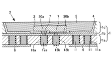
図7には、発光デバイス2の他の形態が示されている。本形態の発光デバイスと、先に述べた実施形態の相違点は、支持基板1が3つの層1a〜1cから構成されている点、及び、凹部11の平面積が拡張されている点である。
FIG. 7 shows another form of the
本実施形態において、支持基板1は、SOI基板であり、第1基板層を構成する第1シリコン層1a、絶縁層を構成する酸化層1b、及び、第2基板層を構成する第2シリコン層1cを、この順序で積層した構造となっている。
In this embodiment, the
SOI基板としては、その製造法により、SIMOX(Separation by Implantation of Oxygen)方式のものと、貼り合わせ方式の2種類のものが知られているが、何れの方式のSOI基板を用いてもよい。 SIMOX方式のSOI基板として、酸素分子をイオン注入によりシリコン結晶表面から埋め込み、それを高熱で酸化させることにより、シリコン結晶中に酸化シリコンの絶縁層を形成する手法が知られている。このような絶縁層は、埋め込み酸化(BOX;Buried Oxide)層と称される。 As an SOI substrate, two types of substrates, a SIMOX (Separation by Implantation of Oxygen) method and a bonding method, are known depending on the manufacturing method, but any type of SOI substrate may be used. As a SIMOX SOI substrate, a technique is known in which oxygen molecules are implanted from the surface of a silicon crystal by ion implantation and oxidized with high heat to form an insulating layer of silicon oxide in the silicon crystal. Such an insulating layer is referred to as a buried oxide (BOX) layer.
凹部10は、第2シリコン層13の表面を切り抜いて形成されており、その内側面は、開口端に向かうに従って開口面積の拡大する傾斜面となっている。この凹部10は、発光素子3の平面積よりかなり大きい平面積を有しており、発光素子6の外周と、凹部10の内周面との間に蛍光層5が充填されている。また、凹部10の内壁面には、先の実施形態と同様に、反射膜4が付着されている。
The
貫通電極12a,12bは、電気絶縁層13a、13bによって電気絶縁された状態で、第1シリコン層1aを貫通しており、その凹部10側の端部は、酸化層1bを貫通する接続部7とそれぞれ接続されている。接続部7は、発光素子3の両端子30a,30bと接続される。この接続部7も、貫通電極12a,12bと同様に、上記の溶融金属充填法や液状分散系充填法を利用したを用いて形成されたCuなどの金属体であると好ましい。なお、接続部7の形状は、円柱状に限られず、四角柱などの他の形状も採り得る。
The through-
柱状ヒートシンク11は、貫通電極12a,12bと同様に、支持基板1の厚み方向において、第1シリコン層1aを貫通するように設けられて、放熱体6に接続されている。すなわち、柱状ヒートシンク11は、支持基板1の裏面から第1シリコン層1aと酸化層1bとの境界まで延在するように設けられている。また、柱状ヒートシンク11も、上記の溶融金属充填法や液状分散系充填法を利用して形成できる。この構成によると、柱状ヒートシンク11の形成にあたって、酸化層1bをエッチング阻止層として機能させることができる。このため、柱状ヒートシンク11の深さ寸法が、第1シリコン層1aの層厚により画定されるので、エッチングの工程管理が極めて容易になるという利点が得られる。
The
上述したように、本発明に係る照明装置は、支持基板1を含んでおり、この支持基板1は、複数の柱状ヒートシンク11を含んでいる。柱状ヒートシンク11は、支持基板1の厚み方向に設けられているため、発光素子3の発光動作によって生じた熱を、柱状ヒートシンク11によって、支持基板1の外部に放熱し、発光素子3の電極30a,30bと貫通電極12a,12bとを接続する接合部分の接合強度を保存し、電気的接続の信頼性を維持することができ、また、発熱による発光素子3の発光特性の変動を回避することもできる。
As described above, the lighting device according to the present invention includes the
柱状ヒートシンク11は、支持基板1の板面に対して所定の面積占有率をもって分布している。したがって、柱状ヒートシンク11を構成する材料の熱抵抗、及び、柱状ヒートシンク11の占有率を適切に選ぶことにより、発光素子3の発光動作によって生じた熱を、柱状ヒートシンク11によって、支持基板1の外部に効率よく放熱し得る。さらに、柱状ヒートシンク11は、その一端が支持基板1の他面側に導出され、支持基板1の他面に設けられた放熱体6に接続されているため、支持基板1の放熱特性は更に向上し得る。
The
さらに、支持基板1は、第1シリコン層1a及び第2シリコン層1cを含み、複数の柱状ヒートシンク11は、第1シリコン層1aを貫通し、互いに間隔を隔てて、発光素子3の周囲に多数配置されており、複数の柱状ヒートシンク11のそれぞれの一端及び前記第1シリコン層1aは、支持基板1の他面に設けられた放熱体6に共通に接続されている。この構造によれば、シリコン層の良好な放熱特性により、3次元的放熱経路が構成され、照明装置全体としての放熱特性を向上させることができる。即ち、発光素子3で発生した熱を、第1シリコン層1a及び第2シリコン層1cによって集熱し、第1シリコン層1a及び第2シリコン層1cから柱状ヒートシンク11に伝達し、更に、柱状ヒートシンク11から第1シリコン層1aを介して、他のヒートシンク11に伝達し、ヒートシンク11から支持基板1の他面に設けられた放熱体6に伝達し、放熱体6から、支持基板1の面方向に向かって外部に拡散放出することができる。
Furthermore, the
また、複数の柱状ヒートシンク11間は、シリコン層なので、支持基板1は、電導性を有する。従って、柱状ヒートシンク11は、その周りを、電気絶縁層11aによって覆い、柱状ヒートシンク11を、支持基板1から電気的に絶縁する。
Since the space between the plurality of columnar heat sinks 11 is a silicon layer, the
本発明に係る照明装置において、支持基板1は、複数の貫通電極12a,12bを含み、板面に凹部10を有している。貫通電極12a,12bは、支持基板1を厚み方向に貫通し、複数の凹部10のそれぞれに、一端が該凹部10の底面に露出するように2個ずつ配置されている。この支持基板1の凹部10内に発光素子3が配置されている。
In the lighting device according to the present invention, the
発光素子3は、透明結晶層32の光出射面3aの反対側の他面に、P型半導体層311及びN型半導体層313を積層した構造である。そして、凹部10の内部で、P型半導体層311のP側電極30bが一方の貫通電極12bの一端に接続され、N型半導体層313のN側電極30aが、貫通電極12a,12bの他方の一端に接続されている。
The
したがって、発光素子3は、積層方向における透明結晶層32の反対側から電流が注入され、発光素子3の電極30a,30bが光出射面3aに現れない構造を有するから、出射した光を効率よく外部に放射させ得る。さらに、半導体層31で生じた光は、反射膜4によって透明結晶層62における光散乱・吸収作用が抑制され、透明結晶層32の光出射面3aに効果的に導かれる。
Therefore, the
次に、本発明に係る液晶ディスプレイを、図9を参照して説明する。液晶ディスプレイは、液晶パネル8と、バックライト9とを含み、概念上、一般的なコンピュータ用の表示装置や汎用電化製品の液晶表示部に限られず、液晶テレビ、あるいは携帯電話機、携帯ゲーム機、携帯情報端末といった携帯型電子機器にも適用され得る。
Next, a liquid crystal display according to the present invention will be described with reference to FIG. The liquid crystal display includes a
液晶パネル8は、偏向フィルタ、ガラス基板、及び液晶層などから構成された液晶モジュールであって、画像信号に基づき、駆動回路(図示せず)からの電気信号によって駆動される。バックライト9は、図8に示された照明装置であり、複数の発光デバイス2により液晶パネル8をその背面側から照明する。もっとも、バックライト9の形態は、これに限定されず、例えば図3に示された照明装置でもよく、本発明に係る照明装置の何れの形態も取り得ることは言うまでもない。
The
バックライト9において、貫通電極12a,12bはバンプ電極や配線基板を介して電源部と接続され、これにより電力を供給された発光素子3が液晶パネル8に対して光を照射する。また、柱状ヒートシンク11は、放熱体6と接続されて、支持基板1内部の熱を液晶ディスプレイの背面側へと排出する。
In the backlight 9, the through
本発明に係る液晶ディスプレイは、上述した照明装置を含むから、既に述べた作用効果を奏する。 Since the liquid crystal display according to the present invention includes the above-described illumination device, the above-described effects can be obtained.
次に、本発明に係る発光ダイオードディスプレイを、図10と図11とを参照して説明する。発光ダイオードディスプレイは、発光素子自体を画素として用いることから、バックライトを必要とせず、消費電力を低減し得るという利点を有する。 Next, a light emitting diode display according to the present invention will be described with reference to FIGS. Since the light emitting diode display uses the light emitting element itself as a pixel, it does not require a backlight and has an advantage that power consumption can be reduced.
図10には、発光ダイオードディスプレイの画素20が平面視で示されており、一方、図11には、この画素20を支持基板1にマトリックス状に配置した発光ダイオードディスプレイが示されている。
FIG. 10 shows a
1個の画素20は、3個の上記発光デバイス2を有しており、これらの発光デバイス20は、赤色光を発する発光素子3R、緑色光を発する発光素子3R、及び青色光を発する発光素子3Rをそれぞれ有している。本実施形態の発光ダイオードディスプレイは、フルカラー表示を前提としているため、このように3色の発光素子3R,3G,3Bを有するが、これに限定されるものではない。例えば、1色のみの表示を前提とする場合、画素20は、3色の発光素子3R,3G,3Bのいずれか1個で構成すればよい。すなわち、画素20は、表示機能に応じた発光素子を有する発光デバイス2を、適宜に選択して構成される。
One
また、本実施形態の画素20は、図示されるように、3個の発光デバイス2が三角形の各頂点の位置に配置されているが、これに限定されず、3色の発光素子3R,3G,3Bの特性に応じて適宜な配置態様を採り得る。
Further, in the
本発明に係る発光ダイオードディスプレイは、各発光素子3R,3G,3Bの貫通電極12a,12bが薄膜トランジスタ(TFT)などと接続され、これにより、各画素20は、画像信号に基づき、駆動回路によって発光制御される。また、柱状ヒートシンク11は、図9に示された構成と同様に、放熱体6と接続されて、支持基板1内部の熱をディスプレイの背面側へと排出する。
In the light emitting diode display according to the present invention, the through
本発明に係る発光ダイオードディスプレイは、上述した照明装置と同じ構成を含むから、既に述べた作用効果を奏する。 Since the light-emitting diode display according to the present invention includes the same configuration as that of the above-described illumination device, the above-described effects can be obtained.
また、本発明に係る信号灯は、例えば鉄道信号機や交通信号機に適用されるものであり、上述した発光ダイオードディスプレイのように、複数の発光デバイス20が配列されて構成され、例えば複数色の発光素子3R,3G,3Bを備える。
The signal lamp according to the present invention is applied to, for example, a railway traffic signal or a traffic signal, and includes a plurality of light emitting
本発明に係る信号灯は、上述した照明装置と同様の構成を含むから、既に述べた作用効果を奏する。 Since the signal lamp according to the present invention includes the same configuration as that of the lighting device described above, the above-described effects can be obtained.
以上、好ましい実施例を参照して本発明の内容を具体的に説明したが、本発明の基本的技術思想及び教示に基づいて、当業者であれば、種々の変形態様を採り得ることは自明である。 Although the contents of the present invention have been specifically described above with reference to the preferred embodiments, it is obvious that those skilled in the art can take various modifications based on the basic technical idea and teachings of the present invention. It is.
1 支持基板
2 発光デバイス
3 発光素子
10 凹部
11 柱状ヒートシンク
12a,12b 貫通電極
20 画素
30a N側電極
30b P側電極
311 P型半導体層
312 N型半導体層
DESCRIPTION OF
Claims (5)
前記支持基板は、板面に複数の発光素子設置領域が設けられ、複数の貫通電極と、複数の柱状ヒートシンクとを含んでおり、
前記複数の貫通電極は、前記支持基板を厚み方向に貫通し、前記複数の発光素子設置領域のそれぞれに、一端が露出するように2個ずつ配置されており、
前記複数の柱状ヒートシンクは、前記支持基板の厚み方向に設けられており、
前記複数の発光素子は、それぞれ、P型半導体層及びN型半導体層を積層した構造を含み、前記支持基板の前記発光素子設置領域に配置され、前記P型半導体層のP側電極が、前記貫通電極の一方の前記一端に接続され、前記N型半導体層のN側電極が、前記貫通電極の他方の前記一端に接続されており、
更に、前記支持基板は、シリコン層を含み、
前記複数の柱状ヒートシンクは、前記シリコン層を貫通し、互いに間隔を隔てて、前記発光素子の周囲に多数配置されており、前記支持基板との間に設けられた電気絶縁層によって前記支持基板から電気絶縁されており、
前記複数の柱状ヒートシンクのそれぞれの一端は、前記支持基板の他面に設けられた放熱体に共通に接続されている、
照明装置。 A lighting device including a support substrate and a plurality of light emitting elements,
The support substrate is provided with a plurality of light emitting element installation regions on a plate surface, and includes a plurality of through electrodes and a plurality of columnar heat sinks,
The plurality of through electrodes are arranged in two so as to penetrate the support substrate in the thickness direction, and to expose one end of each of the plurality of light emitting element installation regions,
The plurality of columnar heat sinks are provided in the thickness direction of the support substrate,
Each of the plurality of light-emitting elements includes a structure in which a P-type semiconductor layer and an N-type semiconductor layer are stacked, and is disposed in the light-emitting element installation region of the support substrate. Connected to one end of the through electrode, and the N-side electrode of the N-type semiconductor layer is connected to the other end of the through electrode,
Further, the support substrate includes a silicon layer,
The plurality of columnar heat sinks penetrates the silicon layer and is arranged around the light emitting element at a distance from each other, and is separated from the support substrate by an electrical insulating layer provided between the support substrate and the plurality of columnar heat sinks. Is electrically insulated,
One end of each of the plurality of columnar heat sinks is commonly connected to a heat radiator provided on the other surface of the support substrate.
Lighting device.
前記バックライトは、請求項1又は2に記載された照明装置であり、前記液晶パネルを背面から照明する、
液晶ディスプレイ。 A liquid crystal display including a liquid crystal panel and a backlight,
The backlight is an illumination device according to claim 1 or 2, and illuminates the liquid crystal panel from the back.
LCD display.
前記支持基板は、板面に複数の発光素子設置領域が設けられ、複数の貫通電極と、複数の柱状ヒートシンクとを含んでおり、
前記複数の貫通電極は、前記支持基板を厚み方向に貫通し、前記複数の発光素子設置領域のそれぞれに、一端が露出するように2個ずつ配置されており、
前記複数の柱状ヒートシンクは、前記支持基板の厚み方向に設けられており、
前記複数の発光素子は、それぞれ、P型半導体層及びN型半導体層を積層した構造を含み、前記支持基板の前記発光素子設置領域に配置され、前記P型半導体層のP側電極が、前記貫通電極の一方の前記一端に接続され、前記N型半導体層のN側電極が、前記貫通電極の他方の前記一端に接続されており、
更に、前記支持基板は、シリコン層を含み、
前記複数の柱状ヒートシンクは、前記シリコン層を貫通し、互いに間隔を隔てて、前記発光素子の周囲に多数配置されており、前記支持基板との間に設けられた電気絶縁層によって前記支持基板から電気絶縁されており、
前記複数の柱状ヒートシンクのそれぞれの一端は、前記支持基板の他面に設けられた放熱体に共通に接続されている、発光ダイオードディスプレイ。 A light-emitting diode display including a support substrate and a plurality of light-emitting elements,
The support substrate is provided with a plurality of light emitting element installation regions on a plate surface, and includes a plurality of through electrodes and a plurality of columnar heat sinks,
The plurality of through electrodes are arranged in two so as to penetrate the support substrate in the thickness direction, and to expose one end of each of the plurality of light emitting element installation regions,
The plurality of columnar heat sinks are provided in the thickness direction of the support substrate,
Each of the plurality of light-emitting elements includes a structure in which a P-type semiconductor layer and an N-type semiconductor layer are stacked, and is disposed in the light-emitting element installation region of the support substrate. Connected to one end of the through electrode, and the N-side electrode of the N-type semiconductor layer is connected to the other end of the through electrode,
Further, the support substrate includes a silicon layer,
The plurality of columnar heat sinks penetrates the silicon layer and is arranged around the light emitting element at a distance from each other, and is separated from the support substrate by an electrical insulating layer provided between the support substrate and the plurality of columnar heat sinks. Is electrically insulated,
One end of each of the plurality of columnar heat sinks is a light emitting diode display commonly connected to a heat radiator provided on the other surface of the support substrate.
前記支持基板は、板面に複数の発光素子設置領域が設けられ、複数の貫通電極と、複数の柱状ヒートシンクとを含んでおり、
前記複数の貫通電極は、前記支持基板を厚み方向に貫通し、前記複数の発光素子設置領域のそれぞれに、一端が露出するように2個ずつ配置されており、
前記複数の柱状ヒートシンクは、前記支持基板の厚み方向に設けられており、
前記複数の発光素子は、それぞれ、P型半導体層及びN型半導体層を積層した構造を含み、前記支持基板の前記発光素子設置領域に配置され、前記P型半導体層のP側電極が、前記貫通電極の一方の前記一端に接続され、前記N型半導体層のN側電極が、前記貫通電極の他方の前記一端に接続されており、
更に、前記支持基板は、シリコン層を含み、
前記複数の柱状ヒートシンクは、前記シリコン層を貫通し、互いに間隔を隔てて、前記発光素子の周囲に多数配置され、前記支持基板との間に設けられた電気絶縁層によって前記支持基板から電気絶縁されており、
前記複数の柱状ヒートシンクのそれぞれの一端は、前記支持基板の他面に設けられた放熱体に共通に接続されている、
信号灯。 A signal lamp including a support substrate and a plurality of light emitting elements,
The support substrate is provided with a plurality of light emitting element installation regions on a plate surface, and includes a plurality of through electrodes and a plurality of columnar heat sinks,
The plurality of through electrodes are arranged in two so as to penetrate the support substrate in the thickness direction, and to expose one end of each of the plurality of light emitting element installation regions,
The plurality of columnar heat sinks are provided in the thickness direction of the support substrate,
Each of the plurality of light-emitting elements includes a structure in which a P-type semiconductor layer and an N-type semiconductor layer are stacked, and is disposed in the light-emitting element installation region of the support substrate. Connected to one end of the through electrode, and the N-side electrode of the N-type semiconductor layer is connected to the other end of the through electrode,
Further, the support substrate includes a silicon layer,
The plurality of columnar heat sinks penetrates the silicon layer, and is arranged around the light emitting element at a distance from each other, and is electrically insulated from the support substrate by an electrical insulation layer provided between the support substrate and the plurality of column heat sinks. Has been
One end of each of the plurality of columnar heat sinks is commonly connected to a heat radiator provided on the other surface of the support substrate.
Signal light.
Priority Applications (1)
| Application Number | Priority Date | Filing Date | Title |
|---|---|---|---|
| JP2012018290A JP5124688B2 (en) | 2011-03-16 | 2012-01-31 | Lighting device, display, and signal lamp |
Applications Claiming Priority (3)
| Application Number | Priority Date | Filing Date | Title |
|---|---|---|---|
| JP2011057542 | 2011-03-16 | ||
| JP2011057542 | 2011-03-16 | ||
| JP2012018290A JP5124688B2 (en) | 2011-03-16 | 2012-01-31 | Lighting device, display, and signal lamp |
Publications (2)
| Publication Number | Publication Date |
|---|---|
| JP2012209537A true JP2012209537A (en) | 2012-10-25 |
| JP5124688B2 JP5124688B2 (en) | 2013-01-23 |
Family
ID=47189005
Family Applications (1)
| Application Number | Title | Priority Date | Filing Date |
|---|---|---|---|
| JP2012018290A Expired - Fee Related JP5124688B2 (en) | 2011-03-16 | 2012-01-31 | Lighting device, display, and signal lamp |
Country Status (1)
| Country | Link |
|---|---|
| JP (1) | JP5124688B2 (en) |
Cited By (6)
| Publication number | Priority date | Publication date | Assignee | Title |
|---|---|---|---|---|
| JP5450780B1 (en) * | 2012-12-21 | 2014-03-26 | 有限会社 ナプラ | Method for forming a conductor in a minute space |
| KR101402177B1 (en) | 2013-11-18 | 2014-06-27 | 김인호 | LED PCB with flat panel type cooling fin |
| WO2017057927A1 (en) * | 2015-10-01 | 2017-04-06 | 엘지이노텍 주식회사 | Light emitting device, method for producing light emitting device, and light emitting module |
| JP2019029673A (en) * | 2017-08-02 | 2019-02-21 | エルジー イノテック カンパニー リミテッド | Light-emitting element package |
| JP2019515507A (en) * | 2016-05-06 | 2019-06-06 | テーデーカー エレクトロニクス アーゲー | Multi LED system |
| JP2020047745A (en) * | 2018-09-19 | 2020-03-26 | パナソニックIpマネジメント株式会社 | Light-emitting device and mobile body comprising the same |
Citations (8)
| Publication number | Priority date | Publication date | Assignee | Title |
|---|---|---|---|---|
| JPH1098127A (en) * | 1996-09-24 | 1998-04-14 | Matsushita Electric Works Ltd | Semiconductor package for surface mounting |
| JP2005158957A (en) * | 2003-11-25 | 2005-06-16 | Matsushita Electric Works Ltd | Light emitting device |
| JP2007134645A (en) * | 2005-11-14 | 2007-05-31 | Shinko Electric Ind Co Ltd | Semiconductor device and method of manufacturing the same |
| JP2007294834A (en) * | 2006-03-28 | 2007-11-08 | Matsushita Electric Works Ltd | Light emitting device |
| JP2007318050A (en) * | 2006-05-29 | 2007-12-06 | Sharp Corp | Light-emitting device, and display apparatus method for controlling the same |
| JP2008294253A (en) * | 2007-05-25 | 2008-12-04 | Ngk Spark Plug Co Ltd | Wiring board for packaging light emitting element |
| JP2010238941A (en) * | 2009-03-31 | 2010-10-21 | Sanyo Electric Co Ltd | Light emitting device |
| JP2011044612A (en) * | 2009-08-21 | 2011-03-03 | Panasonic Electric Works Co Ltd | Light emitting device |
-
2012
- 2012-01-31 JP JP2012018290A patent/JP5124688B2/en not_active Expired - Fee Related
Patent Citations (8)
| Publication number | Priority date | Publication date | Assignee | Title |
|---|---|---|---|---|
| JPH1098127A (en) * | 1996-09-24 | 1998-04-14 | Matsushita Electric Works Ltd | Semiconductor package for surface mounting |
| JP2005158957A (en) * | 2003-11-25 | 2005-06-16 | Matsushita Electric Works Ltd | Light emitting device |
| JP2007134645A (en) * | 2005-11-14 | 2007-05-31 | Shinko Electric Ind Co Ltd | Semiconductor device and method of manufacturing the same |
| JP2007294834A (en) * | 2006-03-28 | 2007-11-08 | Matsushita Electric Works Ltd | Light emitting device |
| JP2007318050A (en) * | 2006-05-29 | 2007-12-06 | Sharp Corp | Light-emitting device, and display apparatus method for controlling the same |
| JP2008294253A (en) * | 2007-05-25 | 2008-12-04 | Ngk Spark Plug Co Ltd | Wiring board for packaging light emitting element |
| JP2010238941A (en) * | 2009-03-31 | 2010-10-21 | Sanyo Electric Co Ltd | Light emitting device |
| JP2011044612A (en) * | 2009-08-21 | 2011-03-03 | Panasonic Electric Works Co Ltd | Light emitting device |
Cited By (12)
| Publication number | Priority date | Publication date | Assignee | Title |
|---|---|---|---|---|
| JP5450780B1 (en) * | 2012-12-21 | 2014-03-26 | 有限会社 ナプラ | Method for forming a conductor in a minute space |
| KR101402177B1 (en) | 2013-11-18 | 2014-06-27 | 김인호 | LED PCB with flat panel type cooling fin |
| WO2017057927A1 (en) * | 2015-10-01 | 2017-04-06 | 엘지이노텍 주식회사 | Light emitting device, method for producing light emitting device, and light emitting module |
| US10811566B2 (en) | 2015-10-01 | 2020-10-20 | Lg Innotek Co., Ltd. | Light emitting device, method for producing light emitting device, and light emitting module |
| JP2019515507A (en) * | 2016-05-06 | 2019-06-06 | テーデーカー エレクトロニクス アーゲー | Multi LED system |
| US10714458B2 (en) | 2016-05-06 | 2020-07-14 | Tdk Electronics Ag | Multi-LED system |
| JP2019029673A (en) * | 2017-08-02 | 2019-02-21 | エルジー イノテック カンパニー リミテッド | Light-emitting element package |
| CN109390449A (en) * | 2017-08-02 | 2019-02-26 | Lg 伊诺特有限公司 | Light emitting device package |
| JP7228871B2 (en) | 2017-08-02 | 2023-02-27 | スージョウ レキン セミコンダクター カンパニー リミテッド | light emitting device package |
| CN109390449B (en) * | 2017-08-02 | 2023-03-28 | 苏州立琻半导体有限公司 | Light emitting device package |
| JP2020047745A (en) * | 2018-09-19 | 2020-03-26 | パナソニックIpマネジメント株式会社 | Light-emitting device and mobile body comprising the same |
| JP7199048B2 (en) | 2018-09-19 | 2023-01-05 | パナソニックIpマネジメント株式会社 | LIGHT-EMITTING DEVICE AND MOVING OBJECT INCLUDING THE SAME |
Also Published As
| Publication number | Publication date |
|---|---|
| JP5124688B2 (en) | 2013-01-23 |
Similar Documents
| Publication | Publication Date | Title |
|---|---|---|
| CN102779932B (en) | Light emitting device package and ultraviolet lamp having the same | |
| JP5124688B2 (en) | Lighting device, display, and signal lamp | |
| KR102031967B1 (en) | Light emitting device package | |
| KR101768720B1 (en) | Surface-mounted led module and method for producing a surface-mounted led module | |
| TWI431819B (en) | Rgb thermal isolation substrate | |
| JP5873108B2 (en) | Wiring board and electronic device | |
| KR20120079445A (en) | Substrate for electronic device and electronic device | |
| JP2012515440A (en) | Multiple light emitting device package | |
| US10629790B2 (en) | Light-emitting device | |
| JP5288642B2 (en) | Light emitting element | |
| EP2533312B1 (en) | Light-emitting diode package | |
| US9425373B2 (en) | Light emitting module | |
| JP2015050303A (en) | Light-emitting device | |
| WO2017188237A1 (en) | Led light source device | |
| JP5888236B2 (en) | LIGHT EMITTING DEVICE, CIRCUIT BOARD, LIGHT EMITTING DEVICE PACKAGE ARRAY, AND LIGHT EMITTING DEVICE PACKAGE ARRAY MANUFACTURING METHOD | |
| CN103579129B (en) | Semiconductor component support and semiconductor device | |
| TWI395346B (en) | Light emitting device package structure and fabricating method thereof | |
| JP2009010308A (en) | Light emitting device | |
| US7943430B2 (en) | Semiconductor device with heat sink and method for manufacturing the same | |
| JP6210720B2 (en) | LED package | |
| JP5709718B2 (en) | Light emitting device | |
| KR101135580B1 (en) | Light Emitting Diode lamp module | |
| JP4657374B1 (en) | Light emitting diode, light emitting device, lighting device, and display | |
| JP2009038156A (en) | Circuit board, and lighting device | |
| JP6569217B2 (en) | Light emitting device |
Legal Events
| Date | Code | Title | Description |
|---|---|---|---|
| A975 | Report on accelerated examination |
Free format text: JAPANESE INTERMEDIATE CODE: A971005 Effective date: 20120727 |
|
| A131 | Notification of reasons for refusal |
Free format text: JAPANESE INTERMEDIATE CODE: A131 Effective date: 20120801 |
|
| A521 | Request for written amendment filed |
Free format text: JAPANESE INTERMEDIATE CODE: A523 Effective date: 20120924 |
|
| TRDD | Decision of grant or rejection written | ||
| A01 | Written decision to grant a patent or to grant a registration (utility model) |
Free format text: JAPANESE INTERMEDIATE CODE: A01 Effective date: 20121017 |
|
| A01 | Written decision to grant a patent or to grant a registration (utility model) |
Free format text: JAPANESE INTERMEDIATE CODE: A01 |
|
| A61 | First payment of annual fees (during grant procedure) |
Free format text: JAPANESE INTERMEDIATE CODE: A61 Effective date: 20121029 |
|
| FPAY | Renewal fee payment (event date is renewal date of database) |
Free format text: PAYMENT UNTIL: 20151102 Year of fee payment: 3 |
|
| R150 | Certificate of patent or registration of utility model |
Ref document number: 5124688 Country of ref document: JP Free format text: JAPANESE INTERMEDIATE CODE: R150 Free format text: JAPANESE INTERMEDIATE CODE: R150 |
|
| R250 | Receipt of annual fees |
Free format text: JAPANESE INTERMEDIATE CODE: R250 |
|
| R250 | Receipt of annual fees |
Free format text: JAPANESE INTERMEDIATE CODE: R250 |
|
| R250 | Receipt of annual fees |
Free format text: JAPANESE INTERMEDIATE CODE: R250 |
|
| R250 | Receipt of annual fees |
Free format text: JAPANESE INTERMEDIATE CODE: R250 |
|
| R250 | Receipt of annual fees |
Free format text: JAPANESE INTERMEDIATE CODE: R250 |
|
| R250 | Receipt of annual fees |
Free format text: JAPANESE INTERMEDIATE CODE: R250 |
|
| LAPS | Cancellation because of no payment of annual fees |