JP2012167174A - Adhesive composition, adhesive sheet, and method of manufacturing semiconductor device - Google Patents
Adhesive composition, adhesive sheet, and method of manufacturing semiconductor device Download PDFInfo
- Publication number
- JP2012167174A JP2012167174A JP2011028835A JP2011028835A JP2012167174A JP 2012167174 A JP2012167174 A JP 2012167174A JP 2011028835 A JP2011028835 A JP 2011028835A JP 2011028835 A JP2011028835 A JP 2011028835A JP 2012167174 A JP2012167174 A JP 2012167174A
- Authority
- JP
- Japan
- Prior art keywords
- adhesive
- adhesive composition
- adhesive layer
- chip
- thermosetting
- Prior art date
- Legal status (The legal status is an assumption and is not a legal conclusion. Google has not performed a legal analysis and makes no representation as to the accuracy of the status listed.)
- Pending
Links
Classifications
-
- H—ELECTRICITY
- H10—SEMICONDUCTOR DEVICES; ELECTRIC SOLID-STATE DEVICES NOT OTHERWISE PROVIDED FOR
- H10W—GENERIC PACKAGES, INTERCONNECTIONS, CONNECTORS OR OTHER CONSTRUCTIONAL DETAILS OF DEVICES COVERED BY CLASS H10
- H10W72/00—Interconnections or connectors in packages
- H10W72/30—Die-attach connectors
-
- H—ELECTRICITY
- H10—SEMICONDUCTOR DEVICES; ELECTRIC SOLID-STATE DEVICES NOT OTHERWISE PROVIDED FOR
- H10W—GENERIC PACKAGES, INTERCONNECTIONS, CONNECTORS OR OTHER CONSTRUCTIONAL DETAILS OF DEVICES COVERED BY CLASS H10
- H10W74/00—Encapsulations, e.g. protective coatings
Landscapes
- Adhesive Tapes (AREA)
- Adhesives Or Adhesive Processes (AREA)
- Die Bonding (AREA)
- Dicing (AREA)
Abstract
Description
本発明は、半導体ウエハなどをダイシングし半導体チップを得て、半導体チップを有機基板やリードフレーム上にダイボンディングする工程で使用するのに特に適した接着剤組成物、および該接着剤組成物からなる接着剤層を有する接着シート、ならびに該接着シートを用いた半導体装置の製造方法に関する。 The present invention relates to an adhesive composition particularly suitable for use in a process of dicing a semiconductor wafer or the like to obtain a semiconductor chip and die-bonding the semiconductor chip on an organic substrate or a lead frame, and the adhesive composition. The present invention relates to an adhesive sheet having an adhesive layer and a method for manufacturing a semiconductor device using the adhesive sheet.
シリコン、ガリウムヒ素などの半導体ウエハは大径の状態で製造され、この半導体ウエハは、素子小片(半導体チップ)に切断分離(ダイシング)された後に次の工程であるボンディング工程に移されている。この際、半導体ウエハは予め粘着シートに貼着された状態でダイシング、洗浄、乾燥、エキスパンディング、ピックアップの各工程が加えられた後、次工程のボンディング工程に移送される。 A semiconductor wafer made of silicon, gallium arsenide, or the like is manufactured in a large diameter state, and the semiconductor wafer is cut and separated (diced) into element pieces (semiconductor chips) and then transferred to a bonding process which is the next process. At this time, the semiconductor wafer is subjected to dicing, cleaning, drying, expanding, and pick-up processes in a state where it is adhered to the adhesive sheet in advance, and then transferred to the next bonding process.
これらの工程の中でピックアップ工程とボンディング工程のプロセスを簡略化するために、ウエハ固定機能とダイ接着機能とを同時に兼ね備えたダイシング・ダイボンディング用接着シートが種々提案されている(たとえば、特許文献1〜4参照)。ダイシング・ダイボンディング用接着シートの接着剤層は、ウエハのダイシング時にはウエハを固定し、ダイシング時にウエハとともにダイシングされ、チップと同形状の接着剤に切断される。その後、チップのピックアップを行うと、チップ裏面に接着剤層が残着した状態でピックアップされる。チップ裏面に残着した接着剤層を介して、チップをリードフレーム等のチップ搭載部に載置し、接着剤層を熱硬化することで、ダイボンドが完了する。次いで、樹脂封止して半導体装置が得られる。その後、半田リフローなどにより半導体装置を所望の箇所に実装する。
上記のように、半導体チップは接着剤層を介してリードフレームに固着されるが、近年接着剤層の変形による種々の不具合が指摘されるようになった。チップと同形状であるべき接着剤層が変形し、チップ端部において、チップと接着剤層との接触面積が減少し、チップとリードフレームとの間に隙間が発生することがある。チップとリードフレームとの間に隙間が発生すると、封止樹脂がこの隙間に浸入する。その結果、樹脂封止の充填具合が不均一になり、熱衝撃に対する耐性が低下し、チップクラックの要因となる。 As described above, the semiconductor chip is fixed to the lead frame via the adhesive layer, but recently various problems due to deformation of the adhesive layer have been pointed out. The adhesive layer that should have the same shape as the chip may be deformed, the contact area between the chip and the adhesive layer may be reduced at the chip end, and a gap may be generated between the chip and the lead frame. When a gap is generated between the chip and the lead frame, the sealing resin enters the gap. As a result, the filling condition of the resin sealing becomes non-uniform, the resistance to thermal shock is lowered, and this causes a chip crack.
また、接着剤層が変形する結果、接着剤層の厚みが不均一になり、ダイボンドされたチップが傾くことがあった。チップが傾くと、ワイヤボンドが困難ないし不可能になり、半導体装置の製造歩留まりが低下する。 Further, as a result of the deformation of the adhesive layer, the thickness of the adhesive layer becomes non-uniform, and the die-bonded chip sometimes tilts. When the chip is tilted, wire bonding becomes difficult or impossible, and the manufacturing yield of the semiconductor device decreases.
このような接着剤層の変形による不具合は、特に半導体装置の小型化のために、チップが薄型化、微小化したために、近年に至って顕在化したと考えられる。チップを薄型化、微小化すると、ダイシングソーにより切断される接着剤層の割合が相対的に増加する。すなわち、ウエハが薄くなると、ウエハと接着剤層の全厚に対する接着剤層の相対厚が増加する。 It is considered that such a problem due to the deformation of the adhesive layer has become apparent in recent years because the chip is thinned and miniaturized especially for downsizing of the semiconductor device. When the chip is thinned and miniaturized, the ratio of the adhesive layer cut by the dicing saw relatively increases. That is, as the wafer becomes thinner, the relative thickness of the adhesive layer with respect to the total thickness of the wafer and the adhesive layer increases.
半導体ウエハをダイシングする際には、ウエハ表面に水を噴霧することで、ダイシング時に発生した熱や屑を除去している。しかし、水はウエハ表面に噴霧されるため、接着剤層における熱の除去効率は低い。切断される接着剤層の量が増加する結果、接着剤層で発生する摩擦熱も増大し、摩擦熱により接着剤層が溶融、変形するために、上記の問題が顕在化したと考えられる。 When dicing a semiconductor wafer, water and spray generated on the wafer surface are removed by spraying water onto the wafer surface. However, since water is sprayed on the wafer surface, the heat removal efficiency in the adhesive layer is low. As a result of the increase in the amount of the adhesive layer to be cut, the frictional heat generated in the adhesive layer also increases, and the adhesive layer is melted and deformed by the frictional heat, so that the above problem is considered to be obvious.
接着剤層の溶融による変形を抑制するためには、接着剤層を構成する接着剤組成物の熱硬化前の溶融粘度を増大させることが有効であり、そのためには、接着剤組成物中のアクリル重合体の量を増加させればよい。しかし、アクリル重合体は、三次元的な高次構造の生成には寄与しないため、アクリル重合体の量を増加させると、接着剤組成物の熱硬化後の貯蔵弾性率が低下してしまう。また、アクリル重合体の量を増加させると、チップの固着に関与する成分、具体的にはエポキシ系熱硬化性樹脂の相対的な量が減少し、チップの固着が不十分になり、最終的に得られる半導体装置のパッケージ信頼性が低下することがある。 In order to suppress deformation due to melting of the adhesive layer, it is effective to increase the melt viscosity before thermosetting of the adhesive composition constituting the adhesive layer. For that purpose, in the adhesive composition What is necessary is just to increase the quantity of an acrylic polymer. However, since the acrylic polymer does not contribute to the generation of a three-dimensional higher order structure, when the amount of the acrylic polymer is increased, the storage elastic modulus of the adhesive composition after thermosetting is lowered. In addition, when the amount of the acrylic polymer is increased, the components involved in chip fixation, specifically, the relative amount of the epoxy-based thermosetting resin is reduced, and the chip fixation becomes insufficient. The package reliability of the obtained semiconductor device may be reduced.
このように、接着剤組成物の熱硬化前における溶融粘度の増加と、熱硬化後の貯蔵弾性率の維持は両立し難い特性であるため、接着剤層の変形を抑制しつつ、ワイヤボンディング適性を維持することは、困難であった。 As described above, since the increase in melt viscosity before thermosetting of the adhesive composition and the maintenance of the storage elastic modulus after thermosetting are difficult to achieve at the same time, it is suitable for wire bonding while suppressing deformation of the adhesive layer. It was difficult to maintain.
したがって、本発明は、ウエハ固定機能とダイ接着機能とを同時に兼ね備えたダイシング・ダイボンディング用接着シートの接着剤層に用いられる接着剤組成物において、熱硬化前の溶融粘度および熱硬化後の貯蔵弾性率を適切に制御することにより、接着剤層の変形を抑制しつつ、ワイヤボンディング適性を維持し、得られる半導体パッケージの信頼性向上を図ることを目的としている。 Accordingly, the present invention relates to an adhesive composition used for an adhesive layer of an adhesive sheet for dicing die bonding that has both a wafer fixing function and a die bonding function at the same time, and a melt viscosity before thermosetting and storage after thermosetting. An object of the present invention is to maintain the wire bonding suitability while suppressing the deformation of the adhesive layer by appropriately controlling the elastic modulus and to improve the reliability of the obtained semiconductor package.
上記課題を解決する本発明は、以下の要旨を要旨として含む。
(1)アクリル重合体(A)、エポキシ系熱硬化性樹脂(B)、および熱硬化剤(C)を含む接着剤組成物であって、
熱硬化前の接着剤組成物の80℃における溶融粘度が1.0×10⁴Pa・s以上であり、かつ、熱硬化後の接着剤組成物の170℃における貯蔵弾性率E’が1.0×10⁷Pa以上である接着用組成物。
The present invention for solving the above problems includes the following gist as a gist.
(1) An adhesive composition comprising an acrylic polymer (A), an epoxy thermosetting resin (B), and a thermosetting agent (C),
The melt viscosity at 80 ° C. of the adhesive composition before thermosetting is 1.0 × 10 4 Pa · s or more, and the storage elastic modulus E ′ at 170 ° C. of the adhesive composition after thermosetting is 1. An adhesive composition that is 0 × 10 7 Pa or more.
(2)上記(1)に記載の接着剤組成物をフィルム状に成膜してなるフィルム状接着剤組成物。 (2) A film adhesive composition obtained by forming the adhesive composition according to (1) into a film.
(3)上記(2)に記載のフィルム状接着剤組成物からなる接着剤層が基材上に剥離可能に形成されてなる接着シート。 (3) An adhesive sheet in which an adhesive layer made of the film adhesive composition according to (2) is formed on a substrate so as to be peelable.
(4)上記(3)に記載の接着シートの接着剤層に半導体ウエハを貼着し、該半導体ウエハをダイシングして半導体チップとし、該半導体チップ裏面に該接着剤層を固着残存させて基材から剥離し、該半導体チップをダイパッド部上、または別の半導体チップ上に該接着剤層を介して載置する工程を含む半導体装置の製造方法。 (4) A semiconductor wafer is attached to the adhesive layer of the adhesive sheet described in (3) above, and the semiconductor wafer is diced to form a semiconductor chip, and the adhesive layer is fixed and left on the back surface of the semiconductor chip. A method for manufacturing a semiconductor device, comprising a step of peeling from a material and placing the semiconductor chip on a die pad portion or another semiconductor chip via the adhesive layer.
本発明によれば、ダイシング・ダイボンディング用接着シートの接着剤層の変形を抑制しつつ、ワイヤボンディング適性を維持することができ、半導体パッケージの信頼性、歩留まりの向上が可能になる。 ADVANTAGE OF THE INVENTION According to this invention, wire bonding aptitude can be maintained, suppressing the deformation | transformation of the adhesive bond layer of the adhesive sheet for dicing die bonding, and the reliability of a semiconductor package and a yield can be improved.
以下、本発明について、その最良の形態も含めてさらに具体的に説明する。本発明に係る接着剤組成物は、アクリル重合体(A)、エポキシ系熱硬化性樹脂(B)、および熱硬化剤(C)を含み、熱硬化前の溶融粘度および熱硬化後の貯蔵弾性率E’が特定範囲に制御されてなることを特徴としている。接着剤組成物には、さらに、各種物性を改良するため、必要に応じ他の成分が含まれていてもよい。まず、これら各成分について具体的に説明する。 Hereinafter, the present invention will be described more specifically, including its best mode. The adhesive composition according to the present invention includes an acrylic polymer (A), an epoxy thermosetting resin (B), and a thermosetting agent (C), and includes a melt viscosity before thermosetting and storage elasticity after thermosetting. It is characterized in that the rate E ′ is controlled within a specific range. In order to improve various physical properties, the adhesive composition may further contain other components as necessary. First, each of these components will be specifically described.
(A)アクリル重合体
接着剤組成物に十分な接着性および造膜性(シート加工性)を付与するためにアクリル重合体(A)が用いられる。アクリル重合体(A)としては、従来公知のアクリル重合体を用いることができる。
(A) Acrylic polymer The acrylic polymer (A) is used to impart sufficient adhesiveness and film forming property (sheet processability) to the adhesive composition. A conventionally well-known acrylic polymer can be used as an acrylic polymer (A).
アクリル重合体(A)の重量平均分子量(Mw)は、1万〜200万であることが望ましく、10万〜150万であることがより望ましく、20万〜120万であることが最も好ましい。アクリル重合体(A)の重量平均分子量が低過ぎると接着剤層と基材との粘着力が高くなり、ピックアップ不良が起こることがあり、また、熱硬化前の接着剤組成物の溶融粘度が低下する傾向にある。一方、アクリル重合体(A)の重量平均分子量が高過ぎると、溶融粘度は増大するものの、チップ搭載部の凹凸へ接着剤層が追従できないことがあり、ボイドなどの発生要因になることがある。 The weight average molecular weight (Mw) of the acrylic polymer (A) is preferably 10,000 to 2,000,000, more preferably 100,000 to 1,500,000, and most preferably 200,000 to 1,200,000. If the weight average molecular weight of the acrylic polymer (A) is too low, the adhesive force between the adhesive layer and the substrate becomes high, and pick-up failure may occur, and the melt viscosity of the adhesive composition before thermosetting is low. It tends to decrease. On the other hand, if the weight average molecular weight of the acrylic polymer (A) is too high, the melt viscosity increases, but the adhesive layer may not follow the irregularities of the chip mounting portion, which may cause voids and the like. .
アクリル重合体(A)のガラス転移温度(Tg)は、好ましくは−60〜50℃、さらに好ましくは−50〜40℃、特に好ましくは−40〜30℃の範囲にある。アクリル重合体(A)のガラス転移温度が低過ぎると接着剤層と基材との剥離力が大きくなってチップのピックアップ不良が起こることがある。一方、アクリル重合体(A)の重量平均分子量が高過ぎると、ウエハを固定するための接着力が不十分となるおそれがある。 The glass transition temperature (Tg) of the acrylic polymer (A) is preferably -60 to 50 ° C, more preferably -50 to 40 ° C, and particularly preferably -40 to 30 ° C. If the glass transition temperature of the acrylic polymer (A) is too low, the peeling force between the adhesive layer and the substrate may be increased, resulting in chip pickup failure. On the other hand, when the weight average molecular weight of the acrylic polymer (A) is too high, the adhesive force for fixing the wafer may be insufficient.
上記アクリル重合体(A)を構成するモノマーとしては、(メタ)アクリル酸エステルモノマーまたはその誘導体が挙げられる。例えば、アルキル基の炭素数が1〜18であるアルキル(メタ)アクリレート、例えばメチル(メタ)アクリレート、エチル(メタ)アクリレート、プロピル(メタ)アクリレート、ブチル(メタ)アクリレート、2−エチルヘキシル(メタ)アクリレートなどが挙げられ;環状骨格を有する(メタ)アクリレート、例えばシクロアルキル(メタ)アクリレート、ベンジル(メタ)アクリレート、イソボルニル(メタ)アクリレート、ジシクロペンタニル(メタ)アクリレート、ジシクロペンテニル(メタ)アクリレート、ジシクロペンテニルオキシエチル(メタ)アクリレート、イミド(メタ)アクリレートなどが挙げられ;水酸基を有するヒドロキシメチル(メタ)アクリレート、2−ヒドロキシエチル(メタ)アクリレート、2−ヒドロキシプロピル(メタ)アクリレートなどが挙げられ;その他、エポキシ基を有するグリシジル(メタ)アクリレートなどが挙げられる。これらの中では、水酸基を有しているモノマーを重合して得られるアクリル重合体が、後述するエポキシ系熱硬化性樹脂(B)との相溶性が良いため好ましい。アクリル重合体を構成するモノマーとして、グリシジル(メタ)アクリレートを含有することにより、後述するエポキシ系熱硬化性樹脂と熱硬化剤との熱硬化による生成される三次元的な高次構造に取り込まれ、熱硬化後の接着剤組成物の貯蔵弾性率が高くなることがある。また、上記アクリル重合体(A)は、アクリル酸、メタクリル酸、イタコン酸、酢酸ビニル、アクリロニトリル、スチレンなどが共重合されていてもよい。 As a monomer which comprises the said acrylic polymer (A), a (meth) acrylic acid ester monomer or its derivative (s) is mentioned. For example, an alkyl (meth) acrylate having an alkyl group having 1 to 18 carbon atoms, such as methyl (meth) acrylate, ethyl (meth) acrylate, propyl (meth) acrylate, butyl (meth) acrylate, 2-ethylhexyl (meth) (Meth) acrylates having a cyclic skeleton such as cycloalkyl (meth) acrylate, benzyl (meth) acrylate, isobornyl (meth) acrylate, dicyclopentanyl (meth) acrylate, dicyclopentenyl (meth) Acrylate, dicyclopentenyloxyethyl (meth) acrylate, imide (meth) acrylate, and the like; hydroxymethyl (meth) acrylate having a hydroxyl group, 2-hydroxyethyl (meth) acrylate, 2-hydride Kishipuropiru (meth) acrylate and the like; other, such as glycidyl (meth) acrylate having an epoxy group. In these, the acrylic polymer obtained by superposing | polymerizing the monomer which has a hydroxyl group has preferable compatibility with the epoxy-type thermosetting resin (B) mentioned later. By containing glycidyl (meth) acrylate as a monomer that constitutes the acrylic polymer, it is incorporated into a three-dimensional higher-order structure that is generated by thermal curing of an epoxy-based thermosetting resin and a thermosetting agent described later. The storage elastic modulus of the adhesive composition after heat curing may be increased. The acrylic polymer (A) may be copolymerized with acrylic acid, methacrylic acid, itaconic acid, vinyl acetate, acrylonitrile, styrene, or the like.
(B)エポキシ系熱硬化性樹脂
エポキシ系熱硬化性樹脂(B)としては、種々のエポキシ樹脂を用いることができ、具体的には、多官能系エポキシ樹脂や、ビフェニル化合物、ビスフェノールAジグリシジルエーテルやその水添物、オルソクレゾールノボラックエポキシ樹脂、ジシクロペンタジエン型エポキシ樹脂、ビフェニル型エポキシ樹脂、ビスフェノールA型エポキシ樹脂、ビスフェノールF型エポキシ樹脂、フェニレン骨格型エポキシ樹脂など、分子中に2官能以上有するエポキシ化合物が挙げられる。これらは1種単独で、または2種以上を組み合わせて用いることができる。
(B) Epoxy thermosetting resin As the epoxy thermosetting resin (B), various epoxy resins can be used. Specifically, polyfunctional epoxy resins, biphenyl compounds, bisphenol A diglycidyl are used. Ether or its hydrogenated product, orthocresol novolac epoxy resin, dicyclopentadiene type epoxy resin, biphenyl type epoxy resin, bisphenol A type epoxy resin, bisphenol F type epoxy resin, phenylene skeleton type epoxy resin, etc. The epoxy compound which has is mentioned. These can be used individually by 1 type or in combination of 2 or more types.
本発明の接着剤組成物には、アクリル重合体(A)100質量部に対して、エポキシ系熱硬化性樹脂(B)が、好ましくは1〜1500質量部含まれ、より好ましくは10〜1000質量部、特に好ましくは100〜500質量部含まれる。エポキシ系熱硬化性樹脂(B)の含有量が1質量部未満であると十分な接着性が得られないことがあり、また、熱硬化後の接着剤組成物の貯蔵弾性率が低くなる傾向がある。一方、エポキシ系熱硬化性樹脂(B)の含有量が1500質量部を超えると接着剤層と基材との剥離力が高くなり、ピックアップ不良が起こることがあり、また、アクリル重合体(A)の含有量が相対的に低下するため、熱硬化前の接着剤組成物の溶融粘度が低下する傾向にある。 In the adhesive composition of the present invention, the epoxy thermosetting resin (B) is preferably contained in an amount of 1 to 1500 parts by mass, more preferably 10 to 1000 parts per 100 parts by mass of the acrylic polymer (A). Part by mass, particularly preferably 100 to 500 parts by mass is contained. When the content of the epoxy thermosetting resin (B) is less than 1 part by mass, sufficient adhesiveness may not be obtained, and the storage elastic modulus of the adhesive composition after thermosetting tends to be low. There is. On the other hand, when the content of the epoxy-based thermosetting resin (B) exceeds 1500 parts by mass, the peeling force between the adhesive layer and the base material is increased, and pickup failure may occur, and the acrylic polymer (A ) Content relatively decreases, the melt viscosity of the adhesive composition before thermosetting tends to decrease.
(C)熱硬化剤
熱硬化剤(C)は、エポキシ系熱硬化性樹脂(B)に対する硬化剤として機能する。好ましい熱硬化剤(C)としては、1分子中にエポキシ基と反応しうる官能基を2個以上有する化合物が挙げられる。その官能基としてはフェノール性水酸基、アルコール性水酸基、アミノ基、カルボキシル基および酸無水物などが挙げられる。これらのうち好ましくはフェノール性水酸基、アミノ基、酸無水物などが挙げられ、さらに好ましくはフェノール性水酸基、アミノ基が挙げられる。
(C) Thermosetting agent The thermosetting agent (C) functions as a curing agent for the epoxy thermosetting resin (B). Preferred examples of the thermosetting agent (C) include compounds having two or more functional groups capable of reacting with an epoxy group in one molecule. Examples of the functional group include a phenolic hydroxyl group, an alcoholic hydroxyl group, an amino group, a carboxyl group, and an acid anhydride. Of these, phenolic hydroxyl groups, amino groups, acid anhydrides and the like are preferable, and phenolic hydroxyl groups and amino groups are more preferable.
フェノール系硬化剤の具体的な例としては、多官能系フェノール樹脂、ビフェノール、ノボラック型フェノール樹脂、ジシクロペンタジエン系フェノール樹脂、ザイロック型フェノール樹脂、アラルキルフェノール樹脂が挙げられる。アミン系硬化剤の具体的な例としては、DICY(ジシアンジアミド)が挙げられる。これらは、1種単独で、または2種以上混合して使用することができる。 Specific examples of the phenolic curing agent include polyfunctional phenolic resin, biphenol, novolac type phenolic resin, dicyclopentadiene type phenolic resin, zylock type phenolic resin, and aralkylphenolic resin. A specific example of the amine curing agent is DICY (dicyandiamide). These can be used individually by 1 type or in mixture of 2 or more types.
熱硬化剤(C)の含有量は、エポキシ系熱硬化性樹脂(B)100質量部に対して、0.1〜500質量部であることが好ましく、1〜200質量部であることがより好ましい。熱硬化剤(C)の含有量が少ないと硬化不足で接着性が得られないことがあり、また、熱硬化後の接着剤組成物の貯蔵弾性率が低くなる傾向がある。熱硬化剤(C)の含有量が過剰であると接着剤組成物の吸湿率が高まりパッケージ信頼性を低下させることがある。 The content of the thermosetting agent (C) is preferably 0.1 to 500 parts by mass and more preferably 1 to 200 parts by mass with respect to 100 parts by mass of the epoxy thermosetting resin (B). preferable. If the content of the thermosetting agent (C) is small, the adhesiveness may not be obtained due to insufficient curing, and the storage elastic modulus of the adhesive composition after thermosetting tends to be low. If the content of the thermosetting agent (C) is excessive, the moisture absorption rate of the adhesive composition is increased and the package reliability may be lowered.
(その他の成分)
本発明に係る接着剤組成物は、上記アクリル重合体(A)、エポキシ系熱硬化性樹脂(B)および熱硬化剤(C)に加えて下記成分を含むことができる。
(Other ingredients)
The adhesive composition according to the present invention can contain the following components in addition to the acrylic polymer (A), the epoxy thermosetting resin (B), and the thermosetting agent (C).
(D)硬化促進剤
硬化促進剤(D)は、接着剤組成物の硬化速度を調整するために用いられる。好ましい硬化促進剤としては、トリエチレンジアミン、ベンジルジメチルアミン、トリエタノールアミン、ジメチルアミノエタノール、トリス(ジメチルアミノメチル)フェノールなどの3級アミン類;2−メチルイミダゾール、2−フェニルイミダゾール、2−フェニル−4−メチルイミダゾール、2−フェニル−4,5−ジヒドロキシメチルイミダゾール、2−フェニル−4−メチル−5−ヒドロキシメチルイミダゾールなどのイミダゾール類;トリブチルホスフィン、ジフェニルホスフィン、トリフェニルホスフィンなどの有機ホスフィン類;テトラフェニルホスホニウムテトラフェニルボレート、トリフェニルホスフィンテトラフェニルボレートなどのテトラフェニルボロン塩などが挙げられる。これらは1種単独で、または2種以上混合して使用することができる。
(D) Curing accelerator The curing accelerator (D) is used to adjust the curing rate of the adhesive composition. Preferred curing accelerators include tertiary amines such as triethylenediamine, benzyldimethylamine, triethanolamine, dimethylaminoethanol, tris (dimethylaminomethyl) phenol; 2-methylimidazole, 2-phenylimidazole, 2-phenyl- Imidazoles such as 4-methylimidazole, 2-phenyl-4,5-dihydroxymethylimidazole, 2-phenyl-4-methyl-5-hydroxymethylimidazole; Organic phosphines such as tributylphosphine, diphenylphosphine, triphenylphosphine; And tetraphenylboron salts such as tetraphenylphosphonium tetraphenylborate and triphenylphosphinetetraphenylborate. These can be used individually by 1 type or in mixture of 2 or more types.
硬化促進剤(D)は、エポキシ系熱硬化性樹脂(B)および熱硬化剤(C)の合計100質量部に対して、好ましくは0.01〜10質量部、さらに好ましくは0.1〜1質量部の量で含まれる。硬化促進剤(D)を上記範囲の量で含有することにより、高温度高湿度下に曝されても優れた接着特性を有し、厳しいリフロー条件に曝された場合であっても高いパッケージ信頼性を達成することができる。硬化促進剤(D)の含有量が少ないと硬化不足で十分な接着特性が得られず、過剰であると高い極性をもつ硬化促進剤は高温度高湿度下で接着剤層中を接着界面側に移動し、偏析することによりパッケージの信頼性を低下させる。 The curing accelerator (D) is preferably 0.01 to 10 parts by mass, more preferably 0.1 to 0.1 parts by mass with respect to a total of 100 parts by mass of the epoxy thermosetting resin (B) and the thermosetting agent (C). It is included in an amount of 1 part by mass. By containing the curing accelerator (D) in an amount within the above range, it has excellent adhesive properties even when exposed to high temperatures and high humidity, and high package reliability even when exposed to severe reflow conditions. Sex can be achieved. If the content of the curing accelerator (D) is small, sufficient adhesive properties cannot be obtained due to insufficient curing, and if it is excessive, the curing accelerator having a high polarity will pass through the adhesive layer under high temperature and high humidity. The reliability of the package is lowered by segregation and segregation.
(E)カップリング剤
カップリング剤(E)は、接着剤組成物の被着体に対する接着性、密着性を向上させるために用いてもよい。また、カップリング剤(E)を使用することで、接着剤組成物を硬化して得られる硬化物の耐熱性を損なうことなく、その耐水性を向上することができる。
(E) Coupling agent The coupling agent (E) may be used to improve the adhesion and adhesion of the adhesive composition to the adherend. Moreover, the water resistance can be improved by using a coupling agent (E), without impairing the heat resistance of the hardened | cured material obtained by hardening | curing adhesive composition.
カップリング剤(E)としては、上記アクリル重合体(A)、エポキシ系熱硬化性樹脂(B)などが有する官能基と反応する基を有する化合物が好ましく使用される。カップリング剤(E)としては、シランカップリング剤が望ましい。このようなカップリング剤としてはγ−グリシドキシプロピルトリメトキシシラン、γ−グリシドキシプロピルメチルジエトキシシラン、β−(3,4−エポキシシクロヘキシル)エチルトリメトキシシラン、γ−(メタクリロキシプロピル)トリメトキシシラン、γ−アミノプロピルトリメトキシシラン、N−6−(アミノエチル)−γ−アミノプロピルトリメトキシシラン、N−6−(アミノエチル)−γ−アミノプロピルメチルジエトキシシラン、N−フェニル−γ−アミノプロピルトリメトキシシラン、γ−ウレイドプロピルトリエトキシシラン、γ−メルカプトプロピルトリメトキシシラン、γ−メルカプトプロピルメチルジメトキシシラン、ビス(3−トリエトキシシリルプロピル)テトラスルファン、メチルトリメトキシシラン、メチルトリエトキシシラン、ビニルトリメトキシシラン、ビニルトリアセトキシシラン、イミダゾールシランなどが挙げられる。これらは1種単独で、または2種以上混合して使用することができる。 As the coupling agent (E), a compound having a group that reacts with a functional group of the acrylic polymer (A), the epoxy thermosetting resin (B), or the like is preferably used. As the coupling agent (E), a silane coupling agent is desirable. Such coupling agents include γ-glycidoxypropyltrimethoxysilane, γ-glycidoxypropylmethyldiethoxysilane, β- (3,4-epoxycyclohexyl) ethyltrimethoxysilane, γ- (methacryloxypropyl). ) Trimethoxysilane, γ-aminopropyltrimethoxysilane, N-6- (aminoethyl) -γ-aminopropyltrimethoxysilane, N-6- (aminoethyl) -γ-aminopropylmethyldiethoxysilane, N- Phenyl-γ-aminopropyltrimethoxysilane, γ-ureidopropyltriethoxysilane, γ-mercaptopropyltrimethoxysilane, γ-mercaptopropylmethyldimethoxysilane, bis (3-triethoxysilylpropyl) tetrasulfane, methyltrimethoxy Silane, meth Examples include rutriethoxysilane, vinyltrimethoxysilane, vinyltriacetoxysilane, and imidazolesilane. These can be used individually by 1 type or in mixture of 2 or more types.
カップリング剤(E)は、アクリル重合体(A)およびエポキシ系熱硬化性樹脂(B)の合計100質量部に対して、通常0.1〜20質量部、好ましくは0.2〜10質量部、より好ましくは0.3〜5質量部の割合で含まれる。カップリング剤(E)の含有量が0.1質量部未満だと上記の効果が得られない可能性があり、20質量部を超えるとアウトガスの原因となる可能性がある。 A coupling agent (E) is 0.1-20 mass parts normally with respect to a total of 100 mass parts of an acrylic polymer (A) and an epoxy-type thermosetting resin (B), Preferably it is 0.2-10 mass. Part, more preferably 0.3 to 5 parts by weight. If the content of the coupling agent (E) is less than 0.1 parts by mass, the above effect may not be obtained, and if it exceeds 20 parts by mass, it may cause outgassing.
(F)架橋剤
接着剤組成物の初期接着力および凝集力を調節するために、架橋剤を添加することもできる。架橋剤(F)としては有機多価イソシアネート化合物、有機多価イミン化合物などが挙げられる。
(F) Crosslinking agent A crosslinking agent may be added to adjust the initial adhesive force and cohesive strength of the adhesive composition. Examples of the crosslinking agent (F) include organic polyvalent isocyanate compounds and organic polyvalent imine compounds.
上記有機多価イソシアネート化合物としては、芳香族多価イソシアネート化合物、脂肪族多価イソシアネート化合物、脂環族多価イソシアネート化合物およびこれらの有機多価イソシアネート化合物の三量体、ならびにこれら有機多価イソシアネート化合物とポリオール化合物とを反応させて得られる末端イソシアネートウレタンプレポリマー等を挙げることができる。 Examples of the organic polyvalent isocyanate compound include aromatic polyvalent isocyanate compounds, aliphatic polyvalent isocyanate compounds, alicyclic polyvalent isocyanate compounds, trimers of these organic polyvalent isocyanate compounds, and these organic polyvalent isocyanate compounds. And a terminal isocyanate urethane prepolymer obtained by reacting a polyol compound with a polyol compound.
有機多価イソシアネート化合物としては、たとえば2,4−トリレンジイソシアネート、2,6−トリレンジイソシアネート、1,3−キシレンジイソシアネート、1,4−キシレンジイソシアネート、ジフェニルメタン−4,4’−ジイソシアネート、ジフェニルメタン−2,4’−ジイソシアネート、3−メチルジフェニルメタンジイソシアネート、ヘキサメチレンジイソシアネート、イソホロンジイソシアネート、ジシクロヘキシルメタン−4,4’−ジイソシアネート、ジシクロヘキシルメタン−2,4’−ジイソシアネート、トリメチロールプロパンアダクトトリレンジイソシアネートおよびリジンイソシアネートが挙げられる。 Examples of the organic polyvalent isocyanate compound include 2,4-tolylene diisocyanate, 2,6-tolylene diisocyanate, 1,3-xylene diisocyanate, 1,4-xylene diisocyanate, diphenylmethane-4,4′-diisocyanate, diphenylmethane- 2,4′-diisocyanate, 3-methyldiphenylmethane diisocyanate, hexamethylene diisocyanate, isophorone diisocyanate, dicyclohexylmethane-4,4′-diisocyanate, dicyclohexylmethane-2,4′-diisocyanate, trimethylolpropane adduct tolylene diisocyanate and lysine isocyanate Is mentioned.
上記有機多価イミン化合物としては、N,N’−ジフェニルメタン−4,4’−ビス(1−アジリジンカルボキシアミド)、トリメチロールプロパン−トリ−β−アジリジニルプロピオネート、テトラメチロールメタン−トリ−β−アジリジニルプロピオネートおよびN,N’−トルエン−2,4−ビス(1−アジリジンカルボキシアミド)トリエチレンメラミン等を挙げることができる。 Examples of the organic polyvalent imine compound include N, N′-diphenylmethane-4,4′-bis (1-aziridinecarboxamide), trimethylolpropane-tri-β-aziridinylpropionate, tetramethylolmethane-tri -Β-aziridinylpropionate and N, N′-toluene-2,4-bis (1-aziridinecarboxyamide) triethylenemelamine can be exemplified.
架橋剤(F)はアクリル重合体(A)100質量部に対して通常0.1〜50質量部、好ましくは1〜40質量部、より好ましくは10〜30質量部の比率で用いられる。架橋剤(F)の配合量を増加することで、組成物中に架橋構造が導入され、組成物の溶融粘度は増加する傾向にある。 A crosslinking agent (F) is 0.1-50 mass parts normally with respect to 100 mass parts of acrylic polymers (A), Preferably it is 1-40 mass parts, More preferably, it is used in the ratio of 10-30 mass parts. By increasing the amount of the crosslinking agent (F), a crosslinked structure is introduced into the composition, and the melt viscosity of the composition tends to increase.
(G)エネルギー線重合性化合物
本発明の接着剤組成物において、エネルギー線重合性化合物が配合されていてもよい。エネルギー線重合性化合物(G)を硬化することで、接着剤組成物の接着力を低減でき、後述する基材からの接着剤層の剥離力を適宜に調整することが可能になる。エネルギー線重合性化合物(G)は、エネルギー線重合性基を含み、紫外線、電子線等のエネルギー線の照射を受けると重合硬化する。このようなエネルギー線重合性化合物(G)として具体的には、トリメチロールプロパントリアクリレート、ペンタエリスリトールトリアクリレート、ペンタエリスリトールテトラアクリレート、ジペンタエリスリトールモノヒドロキシペンタアクリレート、ジペンタエリスリトールヘキサアクリレートあるいは1,4−ブチレングリコールジアクリレート、1,6−ヘキサンジオールジアクリレート、ポリエチレングリコールジアクリレート、オリゴエステルアクリレート、ウレタンアクリレート系オリゴマー、エポキシ変性アクリレート、ポリエーテルアクリレートおよびイタコン酸オリゴマーなどのアクリレート系化合物が挙げられる。また、エネルギー線重合性化合物(G)は、ジシクロペンタジエン骨格含有エネルギー線重合性化合物であってもよい。このような化合物は、分子内に少なくとも1つの重合性二重結合を有し、通常は、重量平均分子量が100〜30000、好ましくは300〜10000程度である。
(G) Energy beam polymerizable compound In the adhesive composition of the present invention, an energy beam polymerizable compound may be blended. By curing the energy beam polymerizable compound (G), the adhesive force of the adhesive composition can be reduced, and the peeling force of the adhesive layer from the base material described later can be appropriately adjusted. The energy beam polymerizable compound (G) contains an energy beam polymerizable group and is polymerized and cured when irradiated with energy rays such as ultraviolet rays and electron beams. Specific examples of the energy ray polymerizable compound (G) include trimethylolpropane triacrylate, pentaerythritol triacrylate, pentaerythritol tetraacrylate, dipentaerythritol monohydroxypentaacrylate, dipentaerythritol hexaacrylate, and 1,4. Examples include acrylate compounds such as butylene glycol diacrylate, 1,6-hexanediol diacrylate, polyethylene glycol diacrylate, oligoester acrylate, urethane acrylate oligomer, epoxy-modified acrylate, polyether acrylate, and itaconic acid oligomer. The energy beam polymerizable compound (G) may be a dicyclopentadiene skeleton-containing energy beam polymerizable compound. Such a compound has at least one polymerizable double bond in the molecule, and usually has a weight average molecular weight of about 100 to 30,000, preferably about 300 to 10,000.
エネルギー線重合性化合物(G)の配合量は、特に限定はされないが、接着剤組成物の全量100質量部に対して、1〜50質量部程度の割合で用いることが好ましい。 Although the compounding quantity of an energy-beam polymeric compound (G) is not specifically limited, It is preferable to use in the ratio of about 1-50 mass parts with respect to 100 mass parts of whole quantity of an adhesive composition.
なお、上記アクリル重合体(A)およびエネルギー線重合性化合物(G)の性質を兼ね備えるものとして、主鎖または側鎖に、エネルギー線重合性基が結合されてなるエネルギー線硬化型粘着性重合体を用いてもよい。このようなエネルギー線硬化型粘着性重合体は、粘着性とエネルギー線硬化性とを兼ね備える性質を有する。 In addition, the energy ray-curable pressure-sensitive adhesive polymer in which an energy ray-polymerizable group is bonded to the main chain or the side chain as having the properties of the acrylic polymer (A) and the energy ray-polymerizable compound (G). May be used. Such an energy beam curable adhesive polymer has the property of having both adhesiveness and energy beam curable properties.
(H)光重合開始剤
本発明の接着剤組成物が、前述したエネルギー線重合性化合物(G)等のエネルギー線硬化成分を含有する場合には、その使用に際して、紫外線等のエネルギー線を照射して、エネルギー線重合性化合物を硬化させる。この際、該組成物中に光重合開始剤(H)を含有させることで、重合硬化時間ならびに光線照射量を少なくすることができる。
(H) Photopolymerization initiator When the adhesive composition of the present invention contains an energy ray-curable component such as the energy ray-polymerizable compound (G) described above, energy rays such as ultraviolet rays are irradiated when used. Then, the energy beam polymerizable compound is cured. At this time, by including the photopolymerization initiator (H) in the composition, the polymerization curing time and the amount of light irradiation can be reduced.
このような光重合開始剤(H)として具体的には、ベンゾフェノン、アセトフェノン、ベンゾイン、ベンゾインメチルエーテル、ベンゾインエチルエーテル、ベンゾインイソプロピルエーテル、ベンゾインイソブチルエーテル、ベンゾイン安息香酸、ベンゾイン安息香酸メチル、ベンゾインジメチルケタール、2,4−ジエチルチオキサンソン、α−ヒドロキシシクロヘキシルフェニルケトン、ベンジルジフェニルサルファイド、テトラメチルチウラムモノサルファイド、アゾビスイソブチロニトリル、ベンジル、ジベンジル、ジアセチル、1,2−ジフェニルメタン、2−ヒドロキシ−2−メチル−1−[4−(1−メチルビニル)フェニル]プロパノン、2,4,6−トリメチルベンゾイルジフェニルフォスフィンオキサイドおよびβ−クロールアンスラキノンなどが挙げられる。光重合開始剤(H)は1種類単独で、または2種類以上を組み合わせて用いることができる。 Specific examples of such a photopolymerization initiator (H) include benzophenone, acetophenone, benzoin, benzoin methyl ether, benzoin ethyl ether, benzoin isopropyl ether, benzoin isobutyl ether, benzoin benzoic acid, benzoin methyl benzoate, and benzoin dimethyl ketal. 2,4-diethylthioxanthone, α-hydroxycyclohexyl phenyl ketone, benzyldiphenyl sulfide, tetramethylthiuram monosulfide, azobisisobutyronitrile, benzyl, dibenzyl, diacetyl, 1,2-diphenylmethane, 2-hydroxy- 2-methyl-1- [4- (1-methylvinyl) phenyl] propanone, 2,4,6-trimethylbenzoyldiphenylphosphine oxide and β-alkyl Examples thereof include roll anthraquinone. A photoinitiator (H) can be used individually by 1 type or in combination of 2 or more types.
光重合開始剤(H)の配合割合は、エネルギー線重合性化合物(G)100質量部に対して0.1〜10質量部含まれることが好ましく、1〜5質量部含まれることがより好ましい。0.1質量部未満であると光重合の不足で満足なピックアップ性が得られないことがあり、10質量部を超えると光重合に寄与しない残留物が生成し、接着剤組成物の硬化性が不十分となることがある。 It is preferable that 0.1-10 mass parts is contained with respect to 100 mass parts of energy beam polymeric compounds (G), and, as for the mixture ratio of a photoinitiator (H), it is more preferable that 1-5 mass parts is contained. . If the amount is less than 0.1 parts by mass, a satisfactory pick-up property may not be obtained due to insufficient photopolymerization. If the amount exceeds 10 parts by mass, a residue that does not contribute to photopolymerization is generated, and the curability of the adhesive composition. May be insufficient.
(汎用添加剤)
本発明の接着剤組成物には、上記の他に、必要に応じて各種添加剤が配合されてもよい。各種添加剤としては、熱可塑性樹脂、可塑剤、帯電防止剤、酸化防止剤、無機充填剤、顔料、染料などが挙げられる。
(General-purpose additive)
In addition to the above, various additives may be blended in the adhesive composition of the present invention as necessary. Examples of the various additives include thermoplastic resins, plasticizers, antistatic agents, antioxidants, inorganic fillers, pigments, and dyes.
(接着剤組成物)
本発明に係る接着剤組成物は、上記各成分を適宜の割合で混合して得られる。混合に際しては、各成分を予め溶媒で希釈しておいてもよく、また混合時に溶媒を加えてもよい。
(Adhesive composition)
The adhesive composition according to the present invention is obtained by mixing the above-described components at an appropriate ratio. In mixing, each component may be diluted with a solvent in advance, or a solvent may be added during mixing.
上記のような各成分からなる接着剤組成物は、熱硬化性であり、硬化前には適度な感圧接着性と形状保持性とを有する。そして熱硬化を経て最終的には耐衝撃性の高い硬化物を与えることができ、接着強度にも優れ、厳しい高温度高湿度条件下においても十分な接着特性を保持し得る。 The adhesive composition comprising the above components is thermosetting and has appropriate pressure-sensitive adhesiveness and shape retention before curing. Finally, a cured product having high impact resistance can be obtained through heat curing, and the adhesive strength is excellent, and sufficient adhesive properties can be maintained even under severe high temperature and high humidity conditions.
熱硬化前の接着剤組成物の80℃における溶融粘度は、1.0×10⁴Pa・s以上であり、好ましくは2.0×10⁴Pa・s以上、さらに好ましくは4.0×10⁴Pa・s以上である。ここで、80℃における溶融粘度を規定した理由は、ブレードダイシング時の摩擦熱により、接着剤層が80℃程度までに加熱されることを考慮したものであるが、実際のダイシング時における接着剤層の温度が80℃に限定されることはない。熱硬化前の接着剤組成物の80℃における溶融粘度が上記範囲にあると、ダイシング時の摩擦により接着剤層が加熱された場合であっても、接着剤層の変形を抑制することができる。一方、溶融粘度が高すぎる場合には、感圧接着性が低下することがある。 The melt viscosity at 80 ° C. of the adhesive composition before thermosetting is 1.0 × 10 4 Pa · s or more, preferably 2.0 × 10 4 Pa · s or more, more preferably 4.0 × 10. 4 Pa · s or more. Here, the reason why the melt viscosity at 80 ° C. is specified is that the adhesive layer is heated to about 80 ° C. by frictional heat at the time of blade dicing. The temperature of the layer is not limited to 80 ° C. When the melt viscosity at 80 ° C. of the adhesive composition before thermosetting is in the above range, deformation of the adhesive layer can be suppressed even when the adhesive layer is heated by friction during dicing. . On the other hand, when the melt viscosity is too high, the pressure-sensitive adhesiveness may decrease.
なお、接着剤組成物が、エネルギー線重合性化合物(G)等のエネルギー線硬化成分を含有する場合には、上記溶融粘度は、接着剤組成物のエネルギー線硬化前の溶融粘度であってもよく、エネルギー線硬化後の溶融粘度であってもよい。溶融粘度は、ダイシング時の接着剤層の変形を抑制することを目的として規定されたものであるので、実際のプロセスにおいては、ダイシング時の接着剤層の溶融粘度を意味する。したがって、ダイシングに先立って接着剤層のエネルギー線硬化を行う場合には、溶融粘度は、エネルギー線硬化後、熱硬化前の接着剤層の溶融粘度を意味する。また、貯蔵弾性率E’は、エネルギー線硬化後および熱硬化後の貯蔵弾性率E’を意味する。通常は、ダイシング前にエネルギー線硬化を行うことが多い。 In the case where the adhesive composition contains an energy beam curing component such as an energy beam polymerizable compound (G), the melt viscosity may be the melt viscosity before energy beam curing of the adhesive composition. It may be a melt viscosity after energy beam curing. Since the melt viscosity is defined for the purpose of suppressing deformation of the adhesive layer during dicing, in the actual process, it means the melt viscosity of the adhesive layer during dicing. Therefore, when energy beam curing of the adhesive layer is performed prior to dicing, the melt viscosity means the melt viscosity of the adhesive layer after energy beam curing and before heat curing. The storage elastic modulus E ′ means the storage elastic modulus E ′ after energy beam curing and after heat curing. Usually, energy beam curing is often performed before dicing.
また、熱硬化後の接着剤組成物の170℃における貯蔵弾性率E’は、1.0×10⁷Pa以上、好ましくは2.0×10⁷Pa以上、さらに好ましくは5.0×10⁷Pa以上の範囲にある。ここで、170℃における貯蔵弾性率E’を規定した理由は、ワイヤボンド時における接着剤層の温度を考慮したものであるが、実際のワイヤボンド時における接着剤層が170℃に限定されることはない。熱硬化後の接着剤組成物の170℃における貯蔵弾性率E’が上記範囲にあると、ワイヤボンド時に接着剤層が加熱された場合であっても、接着剤層の振動を抑制でき、ワイヤボンディングを安定して行うことができる。一方、貯蔵弾性率が高すぎる場合には、硬化性化合物が多量に含まれることを意味し、アクリル重合体(A)の相対的な割合が減少するため、熱硬化前の接着剤組成物の溶融粘度が低下する傾向にある。 Further, the storage elastic modulus E ′ at 170 ° C. of the adhesive composition after thermosetting is 1.0 × 10 7 Pa or more, preferably 2.0 × 10 7 Pa or more, more preferably 5.0 × 10 7. It is in the range of Pa or higher. Here, the reason for defining the storage elastic modulus E ′ at 170 ° C. is that the temperature of the adhesive layer at the time of wire bonding is taken into consideration, but the adhesive layer at the time of actual wire bonding is limited to 170 ° C. There is nothing. When the storage elastic modulus E ′ at 170 ° C. of the adhesive composition after thermosetting is in the above range, vibration of the adhesive layer can be suppressed even when the adhesive layer is heated at the time of wire bonding. Bonding can be performed stably. On the other hand, when the storage elastic modulus is too high, it means that a large amount of the curable compound is contained, and the relative proportion of the acrylic polymer (A) is decreased. The melt viscosity tends to decrease.
本発明の接着剤組成物は、アクリル重合体(A)、エポキシ系熱硬化性樹脂(B)および熱硬化剤(C)を含み、熱硬化前の溶融粘度および熱硬化後の貯蔵弾性率E’が特定範囲にある限り、各成分の組成比、各成分の物性、組成物の製法等は特に限定はされない。本発明で使用するアクリル重合体(A)、エポキシ系熱硬化性樹脂(B)および熱硬化剤(C)は何れも公知の範囲から適宜に選択され、その組成比も公知の範囲にある。しかし、アクリル重合体(A)、エポキシ系熱硬化性樹脂(B)および熱硬化剤(C)を含む公知の接着剤組成物では、本発明で規定する溶融粘度および貯蔵弾性率E’が同時に満足されることは無かった。本発明では、成分の組成比を公知の範囲において選択、特定することにより、上記した溶融粘度および貯蔵弾性率E’を達成した。しかしながら、接着剤組成物の溶融粘度および貯蔵弾性率E’は、使用する各成分の特性により変動するので、一義的に組成比を特定することは困難である。 The adhesive composition of the present invention comprises an acrylic polymer (A), an epoxy thermosetting resin (B), and a thermosetting agent (C), and has a melt viscosity before thermosetting and a storage elastic modulus E after thermosetting. As long as' is in the specific range, the composition ratio of each component, the physical properties of each component, the production method of the composition, etc. are not particularly limited. The acrylic polymer (A), epoxy-based thermosetting resin (B) and thermosetting agent (C) used in the present invention are all appropriately selected from a known range, and the composition ratio is also in a known range. However, in the known adhesive composition containing the acrylic polymer (A), the epoxy thermosetting resin (B) and the thermosetting agent (C), the melt viscosity and the storage elastic modulus E ′ specified in the present invention are simultaneously I was never satisfied. In the present invention, the above-described melt viscosity and storage elastic modulus E ′ are achieved by selecting and specifying the composition ratio of the components within a known range. However, since the melt viscosity and the storage elastic modulus E ′ of the adhesive composition vary depending on the characteristics of each component used, it is difficult to uniquely identify the composition ratio.
以下に、本発明で規定する溶融粘度および貯蔵弾性率E’を制御する具体的指針を説明するが、これらは接着剤組成物の物性を特定範囲に制御するための具体的手段の一例であり、何ら限定的に解釈されるべきではない。 Hereinafter, specific guidelines for controlling the melt viscosity and the storage elastic modulus E ′ defined in the present invention will be described. These are examples of specific means for controlling the physical properties of the adhesive composition within a specific range. It should not be interpreted in a limited way.
アクリル重合体(A)の重量平均分子量(Mw)が低下するにつれて、熱硬化前の接着剤組成物の溶融粘度が低下する傾向にある。 As the weight average molecular weight (Mw) of the acrylic polymer (A) decreases, the melt viscosity of the adhesive composition before thermosetting tends to decrease.
また、接着剤組成物中のアクリル重合体(A)の含有割合が多くなると、熱硬化前の接着剤組成物の溶融粘度は増大する傾向にあるが、エポキシ系熱硬化性樹脂(B)の相対的な割合が少なくなるため、熱硬化後の三次元的な高次構造の密度が低下し、貯蔵弾性率が低くなる傾向がある。 Moreover, when the content ratio of the acrylic polymer (A) in the adhesive composition increases, the melt viscosity of the adhesive composition before thermosetting tends to increase, but the epoxy thermosetting resin (B) Since the relative proportion decreases, the density of the three-dimensional higher order structure after thermosetting tends to decrease and the storage elastic modulus tends to decrease.
接着剤組成物中のエポキシ系熱硬化性樹脂(B)の含有割合が少ない場合には、上記のように、熱硬化後の三次元的な高次構造の密度が低下し、貯蔵弾性率が低くなる傾向がある。一方、エポキシ系熱硬化性樹脂(B)の含有割合が多くなると、アクリル重合体(A)の含有量が相対的に低下するため、熱硬化前の接着剤組成物の溶融粘度が低下する傾向にある。 When the content ratio of the epoxy thermosetting resin (B) in the adhesive composition is small, as described above, the density of the three-dimensional higher-order structure after thermosetting is lowered, and the storage elastic modulus is Tend to be lower. On the other hand, when the content ratio of the epoxy-based thermosetting resin (B) increases, the content of the acrylic polymer (A) relatively decreases, so that the melt viscosity of the adhesive composition before thermosetting tends to decrease. It is in.
また、前述したように、接着剤組成物中の架橋剤(F)の配合量を増加することで、組成物中に架橋構造が導入され、組成物の溶融粘度は増加する。したがって、架橋剤の種類および配合量を適宜に選択することで、溶融粘度を調整することができる。 Further, as described above, by increasing the blending amount of the crosslinking agent (F) in the adhesive composition, a crosslinked structure is introduced into the composition, and the melt viscosity of the composition increases. Therefore, the melt viscosity can be adjusted by appropriately selecting the type and blending amount of the crosslinking agent.
(フィルム状接着剤組成物および接着シート)
本発明に係る接着剤組成物は、その形態は特に限定はされないが、取り扱い性等の観点から、フィルム状に成膜して用いることが好ましい。フィルム状の接着剤組成物は、単層品として使用することもできるが、通常は、フィルム状の接着剤組成物(以下、接着剤層と呼ぶ)を基材上に剥離可能に形成してなる接着シートとして用いることが好ましい。本発明に係る接着シートの形状は、テープ状、ラベル状などあらゆる形状をとり得る。
(Film adhesive composition and adhesive sheet)
The form of the adhesive composition according to the present invention is not particularly limited, but it is preferably used after being formed into a film from the viewpoint of handleability and the like. The film-like adhesive composition can be used as a single-layer product, but usually, a film-like adhesive composition (hereinafter referred to as an adhesive layer) is formed on a substrate so as to be peelable. It is preferable to use it as an adhesive sheet. The shape of the adhesive sheet according to the present invention can be any shape such as a tape shape or a label shape.
接着シートの基材は、接着剤層が基材上に剥離可能に形成されていればよく、フィルム上に接着剤層を形成してもよく、粘着シート上に接着剤層を形成してもよい。 As long as the base material of the adhesive sheet is formed so that the adhesive layer can be peeled on the base material, the adhesive layer may be formed on the film, or the adhesive layer may be formed on the pressure-sensitive adhesive sheet. Good.
接着シートの基材としては、たとえば、ポリエチレンフィルム、ポリプロピレンフィルム、ポリブテンフィルム、ポリブタジエンフィルム、ポリメチルペンテンフィルム、ポリ塩化ビニルフィルム、塩化ビニル共重合体フィルム、ポリエチレンテレフタレートフィルム、ポリエチレンナフタレートフィルム、ポリブチレンテレフタレートフィルム、ポリウレタンフィルム、エチレン酢酸ビニル共重合体フィルム、アイオノマー樹脂フィルム、エチレン・(メタ)アクリル酸共重合体フィルム、エチレン・(メタ)アクリル酸エステル共重合体フィルム、ポリスチレンフィルム、ポリカーボネートフィルム、ポリイミドフィルム、フッ素樹脂フィルムなどの透明フィルムが用いられる。またこれらの架橋フィルムも用いられる。さらにこれらの積層フィルムであってもよい。また、これらを着色したフィルム、不透明フィルムなどを用いることができる。 Examples of the base material of the adhesive sheet include polyethylene film, polypropylene film, polybutene film, polybutadiene film, polymethylpentene film, polyvinyl chloride film, vinyl chloride copolymer film, polyethylene terephthalate film, polyethylene naphthalate film, and polybutylene. Terephthalate film, polyurethane film, ethylene vinyl acetate copolymer film, ionomer resin film, ethylene / (meth) acrylic acid copolymer film, ethylene / (meth) acrylic acid ester copolymer film, polystyrene film, polycarbonate film, polyimide A transparent film such as a film or a fluororesin film is used. These crosslinked films are also used. Furthermore, these laminated films may be sufficient. Moreover, the film which colored these, an opaque film, etc. can be used.
本発明に係る接着シートは、各種の被着体に貼付され、被着体に所要の加工を施した後、接着剤層は、被着体に固着残存させて基材から剥離される。すなわち、接着剤層を、基材から被着体に転写する工程を含むプロセスに使用される。このため、基材の接着剤層に接する面の表面張力は、好ましくは40mN/m以下、さらに好ましくは37mN/m以下、特に好ましくは35mN/m以下である。下限値は通常25mN/m程度である。このような表面張力が低い基材は、材質を適宜に選択して得ることが可能であるし、また基材の表面に剥離剤を塗布して剥離処理を施すことで得ることもできる。 The adhesive sheet according to the present invention is affixed to various adherends, and after subjecting the adherend to required processing, the adhesive layer is peeled off from the substrate while remaining adhered to the adherend. That is, it is used in a process including a step of transferring an adhesive layer from a substrate to an adherend. For this reason, the surface tension of the surface in contact with the adhesive layer of the substrate is preferably 40 mN / m or less, more preferably 37 mN / m or less, and particularly preferably 35 mN / m or less. The lower limit is usually about 25 mN / m. Such a substrate having a low surface tension can be obtained by appropriately selecting the material, and can also be obtained by applying a release agent to the surface of the substrate and performing a release treatment.
基材の剥離処理に用いられる剥離剤としては、アルキッド系、シリコーン系、フッ素系、不飽和ポリエステル系、ポリオレフィン系、ワックス系などが用いられるが、特にアルキッド系、シリコーン系、フッ素系の剥離剤が耐熱性を有するので好ましい。 As the release agent used for the substrate release treatment, alkyd, silicone, fluorine, unsaturated polyester, polyolefin, wax, and the like are used. In particular, alkyd, silicone, and fluorine release agents are used. Is preferable because it has heat resistance.
上記の剥離剤を用いて基材の表面を剥離処理するためには、剥離剤をそのまま無溶剤で、または溶剤希釈やエマルション化して、グラビアコーター、メイヤーバーコーター、エアナイフコーター、ロールコーターなどにより塗布して、常温もしくは加熱または電子線硬化させたり、ウェットラミネーションやドライラミネーション、熱溶融ラミネーション、溶融押出ラミネーション、共押出加工などで積層体を形成すればよい。 In order to release the surface of the substrate using the above release agent, the release agent can be applied as it is without solvent, or after solvent dilution or emulsification, using a gravure coater, Mayer bar coater, air knife coater, roll coater, etc. Then, the laminate may be formed by room temperature or heating or electron beam curing, wet lamination, dry lamination, hot melt lamination, melt extrusion lamination, coextrusion processing, or the like.
また、接着シートの基材としては、たとえば、弱粘着力性の再剥離型粘着シートや、エネルギー線照射により粘着力が低下するエネルギー線硬化型粘着シートを用いることができる。 In addition, as the base material of the adhesive sheet, for example, a weakly adhesive re-peelable adhesive sheet or an energy ray curable adhesive sheet whose adhesive strength is reduced by irradiation with energy rays can be used.
基材の厚さは、通常は10〜500μm、好ましくは15〜300μm、特に好ましくは20〜250μm程度である。また、接着剤層の厚みは、通常は1〜500μm、好ましくは5〜300μm、特に好ましくは10〜150μm程度である。 The thickness of the substrate is usually about 10 to 500 μm, preferably about 15 to 300 μm, and particularly preferably about 20 to 250 μm. Moreover, the thickness of an adhesive bond layer is 1-500 micrometers normally, Preferably it is 5-300 micrometers, Most preferably, it is about 10-150 micrometers.
接着シートの製造方法は、特に限定はされず、基材上に、接着剤層を構成する組成物を塗布乾燥することで製造してもよく、また接着剤組成物を剥離フィルム上に塗布乾燥して、フィルム状の接着剤組成物を得て、これを上記基材に転写することで製造してもよい。なお、接着シートの使用前に、接着剤層を保護するために、接着剤層の上面に剥離フィルムを積層しておいてもよい。該剥離フィルムは、ポリエチレンテレフタレートフィルムやポリプロピレンフィルムなどのプラスチック材料にシリコーン樹脂などの剥離剤が塗布されているものが使用される。また、接着剤層の表面外周部には、リングフレームなどの他の治具を固定するために別途粘着剤層や粘着テープが設けられていてもよい。 The method for producing the adhesive sheet is not particularly limited, and the adhesive sheet may be produced by applying and drying the composition constituting the adhesive layer on the substrate, and the adhesive composition may be applied and dried on the release film. And you may manufacture by obtaining a film-form adhesive composition and transferring this to the said base material. In addition, in order to protect an adhesive bond layer before using an adhesive sheet, you may laminate | stack a peeling film on the upper surface of an adhesive bond layer. As the release film, one in which a release agent such as a silicone resin is applied to a plastic material such as a polyethylene terephthalate film or a polypropylene film is used. Further, a pressure-sensitive adhesive layer or a pressure-sensitive adhesive tape may be separately provided on the outer peripheral portion of the surface of the adhesive layer in order to fix another jig such as a ring frame.
次に本発明に係る接着シートの利用方法について、該接着シートを半導体装置の製造に適用した場合を例にとって説明する。 Next, a method of using the adhesive sheet according to the present invention will be described taking as an example the case where the adhesive sheet is applied to the manufacture of a semiconductor device.
(半導体装置の製造方法)
本発明に係る半導体装置の製造方法は、上記接着シートの接着剤層に半導体ウエハを貼着し、該半導体ウエハをダイシングして半導体チップとし、該半導体チップ裏面に接着剤層を固着残存させて基材から剥離し、該半導体チップを有機基板やリードフレームのダイパッド部上、またはチップを積層する場合に別の半導体チップ上に該接着剤層を介して載置する工程を含む。
(Method for manufacturing semiconductor device)
In the method for manufacturing a semiconductor device according to the present invention, a semiconductor wafer is attached to the adhesive layer of the adhesive sheet, the semiconductor wafer is diced into a semiconductor chip, and the adhesive layer is fixedly left on the back surface of the semiconductor chip. A step of peeling from the substrate and placing the semiconductor chip on the die pad portion of the organic substrate or the lead frame, or on another semiconductor chip when the chips are stacked, via the adhesive layer.
以下、本発明に係る半導体装置の製造方法について詳述する。
本発明に係る半導体装置の製造方法においては、まず、表面に回路が形成され、裏面が研削された半導体ウエハを準備する。
Hereinafter, a method for manufacturing a semiconductor device according to the present invention will be described in detail.
In the method for manufacturing a semiconductor device according to the present invention, first, a semiconductor wafer having a circuit formed on the front surface and a ground back surface is prepared.
半導体ウエハはシリコンウエハであってもよく、またガリウム・砒素などの化合物半導体ウエハであってもよい。ウエハ表面への回路の形成はエッチング法、リフトオフ法などの従来より汎用されている方法を含む様々な方法により行うことができる。次いで、半導体ウエハの回路面の反対面(裏面)を研削する。研削法は特に限定はされず、グラインダーなどを用いた公知の手段で研削してもよい。裏面研削時には、表面の回路を保護するために回路面に、表面保護シートと呼ばれる粘着シートを貼付する。裏面研削は、ウエハの回路面側(すなわち表面保護シート側)をチャックテーブル等により固定し、回路が形成されていない裏面側をグラインダーにより研削する。ウエハの研削後の厚みは特に限定はされないが、通常は20〜500μm程度である。 The semiconductor wafer may be a silicon wafer or a compound semiconductor wafer such as gallium / arsenic. Formation of a circuit on the wafer surface can be performed by various methods including conventionally used methods such as an etching method and a lift-off method. Next, the opposite surface (back surface) of the circuit surface of the semiconductor wafer is ground. The grinding method is not particularly limited, and grinding may be performed by a known means using a grinder or the like. At the time of back surface grinding, an adhesive sheet called a surface protection sheet is attached to the circuit surface in order to protect the circuit on the surface. In the back surface grinding, the circuit surface side (that is, the surface protection sheet side) of the wafer is fixed by a chuck table or the like, and the back surface side on which no circuit is formed is ground by a grinder. The thickness of the wafer after grinding is not particularly limited, but is usually about 20 to 500 μm.
その後、必要に応じ、裏面研削時に生じた破砕層を除去する。破砕層の除去は、ケミカルエッチングや、プラズマエッチングなどにより行われる。 Thereafter, if necessary, the crushed layer generated during back grinding is removed. The crushed layer is removed by chemical etching, plasma etching, or the like.
次いで、リングフレームおよび半導体ウエハの裏面側を本発明に係る接着シートの接着剤層上に載置し、軽く押圧し、半導体ウエハを固定する。次いで、接着剤層にエネルギー線重合性化合物(G)が配合されている場合には、接着剤層に基材側からエネルギー線を照射し、エネルギー線重合性化合物(G)を硬化し、接着剤層の凝集力を上げ、接着剤層と基材との間の接着力を低下させておく。照射されるエネルギー線としては、紫外線(UV)または電子線(EB)等が挙げられ、好ましくは紫外線が用いられる。次いで、ダイシングソーなどの切断手段を用いて、上記の半導体ウエハを切断し半導体チップを得る。この際の切断深さは、半導体ウエハの厚みと、接着剤層の厚みとの合計およびダイシングソーの磨耗分を加味した深さにする。接着剤層を本発明の接着剤組成物で構成することで、ダイシング時における接着剤層の変形を抑制することができる。なお、エネルギー線照射は、半導体ウエハの貼付後、半導体チップの剥離(ピックアップ)前のいずれの段階で行ってもよく、たとえばダイシングの後に行ってもよく、また下記のエキスパンド工程の後に行ってもよい。さらにエネルギー線照射を複数回に分けて行ってもよい。 Next, the back side of the ring frame and the semiconductor wafer is placed on the adhesive layer of the adhesive sheet according to the present invention, and lightly pressed to fix the semiconductor wafer. Next, when the energy ray polymerizable compound (G) is blended in the adhesive layer, the energy ray polymerizable compound (G) is cured by irradiating the adhesive layer with energy rays from the substrate side. The cohesive force of the agent layer is increased, and the adhesive force between the adhesive layer and the substrate is lowered. Examples of the energy rays to be irradiated include ultraviolet rays (UV) and electron beams (EB), and preferably ultraviolet rays are used. Next, the semiconductor wafer is cut using a cutting means such as a dicing saw to obtain a semiconductor chip. The cutting depth at this time is a depth that takes into account the sum of the thickness of the semiconductor wafer and the adhesive layer and the wear of the dicing saw. By constituting the adhesive layer with the adhesive composition of the present invention, deformation of the adhesive layer during dicing can be suppressed. The energy beam irradiation may be performed at any stage after the semiconductor wafer is pasted and before the semiconductor chip is peeled off (pickup). For example, the irradiation may be performed after dicing or after the following expanding step. Good. Further, the energy beam irradiation may be performed in a plurality of times.
次いで必要に応じ、接着シートのエキスパンドを行うと、半導体チップ間隔が拡張し、半導体チップのピックアップをさらに容易に行えるようになる。この際、接着剤層と基材との間にずれが発生することになり、接着剤層と基材との間の接着力が減少し、半導体チップのピックアップ性が向上する。このようにして半導体チップのピックアップを行うと、切断された接着剤層を半導体チップ裏面に固着残存させて基材から剥離することができる。 Then, if necessary, when the adhesive sheet is expanded, the interval between the semiconductor chips is expanded, and the semiconductor chips can be picked up more easily. At this time, a deviation occurs between the adhesive layer and the base material, the adhesive force between the adhesive layer and the base material is reduced, and the pick-up property of the semiconductor chip is improved. When the semiconductor chip is picked up in this manner, the cut adhesive layer can be fixedly left on the back surface of the semiconductor chip and peeled off from the substrate.
次いで接着剤層を介して半導体チップを、リードフレームのダイパッド上または別の半導体チップ(下段チップ)表面に載置する(以下、チップが搭載されるダイパッドまたは下段チップ表面を「チップ搭載部」と記載する)。チップ搭載部は、半導体チップを載置する前に加熱するか載置直後に加熱される。加熱温度は、通常は80〜200℃、好ましくは100〜180℃であり、加熱時間は、通常は0.1秒〜5分、好ましくは0.5秒〜3分であり、載置するときの圧力は、通常1kPa〜200MPaである。 Next, the semiconductor chip is placed on the die pad of the lead frame or the surface of another semiconductor chip (lower chip) via the adhesive layer (hereinafter, the die pad or lower chip surface on which the chip is mounted is referred to as “chip mounting portion”. To describe). The chip mounting portion is heated before or after the semiconductor chip is placed. The heating temperature is usually 80 to 200 ° C., preferably 100 to 180 ° C., and the heating time is usually 0.1 seconds to 5 minutes, preferably 0.5 seconds to 3 minutes. The pressure is usually 1 kPa to 200 MPa.
半導体チップをチップ搭載部に載置した後、必要に応じさらに加熱を行ってもよい。この際の加熱条件は、上記加熱温度の範囲であって、加熱時間は通常1〜180分、好ましくは10〜120分である。半導体チップをチップ搭載部に載置した後にワイヤボンディングを行う。この際、接着剤層は加熱され軟化するが、接着剤層を本発明の接着剤組成物で構成することで、ダイボンド時の振動が抑制され、ダイボンドを安定して行うことができる。 After placing the semiconductor chip on the chip mounting portion, further heating may be performed as necessary. The heating conditions at this time are in the above heating temperature range, and the heating time is usually 1 to 180 minutes, preferably 10 to 120 minutes. Wire bonding is performed after the semiconductor chip is placed on the chip mounting portion. Under the present circumstances, although an adhesive bond layer is heated and softened, the vibration at the time of die-bonding can be suppressed and die-bonding can be performed stably by comprising an adhesive bond layer by the adhesive composition of this invention.
また、載置後の加熱処理は行わずに仮接着状態としておき、パッケージ製造において通常行われる樹脂封止での加熱を利用して接着剤層を硬化させてもよい。このような工程を経ることで、接着剤層が硬化し、半導体チップとチップ搭載部とを強固に接着することができる。接着剤層はダイボンド条件下ではフィルム形状を維持しつつもある程度軟化しているため、チップ搭載部の凹凸にも十分に埋め込まれ、ボイドの発生を防止できパッケージの信頼性が高くなる。 Alternatively, the adhesive layer may be cured by using heat in resin sealing that is normally performed in package manufacturing, without temporarily performing the heat treatment after placement. Through such a process, the adhesive layer is cured, and the semiconductor chip and the chip mounting portion can be firmly bonded. Since the adhesive layer is softened to some extent while maintaining the film shape under die-bonding conditions, the adhesive layer is sufficiently embedded in the unevenness of the chip mounting portion, and generation of voids can be prevented and the reliability of the package is improved.
本発明の接着剤組成物および接着シートは、上記のような使用方法の他、半導体化合物、ガラス、セラミックス、金属などの接着に使用することもできる。 The adhesive composition and adhesive sheet of the present invention can be used for bonding semiconductor compounds, glass, ceramics, metals, etc., in addition to the above-described methods of use.
以下、本発明を実施例により説明するが、本発明はこれら実施例に限定されるものではない。なお、以下の実施例および比較例において、<溶融粘度>、<貯蔵弾性率>、<パッケージ信頼性>、<接着剤層の変形>および<ワイヤボンディング適性>は次のように評価した。 EXAMPLES Hereinafter, although an Example demonstrates this invention, this invention is not limited to these Examples. In the following examples and comparative examples, <melt viscosity>, <storage modulus>, <package reliability>, <deformation of adhesive layer>, and <wire bonding aptitude> were evaluated as follows.
<溶融粘度>
実施例、比較例で作成した接着シートの接着剤層(フィルム状接着剤組成物)を、厚さ0.2mmまで積層したのち、その後、直径10mmに打ち抜いたものをさらに厚さ15mmまで積層することで、測定用のサンプルを作成した。なお、接着剤層がエネルギー線重合性化合物(G)を含有する場合には、接着剤層を0.2mmまで積層したのちにエネルギー線(紫外線:230mW/cm2、240mJ/cm2)を照射し、エネルギー線重合性化合物を硬化し、その後、直径10mmに打ち抜いたものをさらに厚さ15mmまで積層することで、測定用のサンプルを作成した。次いで、キャピラリーレオメーター(島津製作所社製,CFT−100D)を用いて、試験開始温度50℃、昇温速度10℃/分、試験力50kgf、ダイ穴径0.5mmφ、ダイ長さ1.0mmの条件で溶融粘度を測定し、熱硬化前の接着剤組成物の80℃における溶融粘度を求めた。
<Melt viscosity>
After laminating the adhesive layer (film adhesive composition) of the adhesive sheet prepared in the examples and comparative examples to a thickness of 0.2 mm, the material punched to a diameter of 10 mm is further laminated to a thickness of 15 mm. Thus, a sample for measurement was created. When the adhesive layer contains the energy beam polymerizable compound (G), the energy layer (ultraviolet rays: 230 mW / cm 2 , 240 mJ / cm 2 ) is irradiated after the adhesive layer is laminated to 0.2 mm. Then, the energy ray-polymerizable compound was cured, and then a sample for measurement was prepared by stacking a material punched to a diameter of 10 mm to a thickness of 15 mm. Next, using a capillary rheometer (manufactured by Shimadzu Corp., CFT-100D), the test start temperature is 50 ° C., the heating rate is 10 ° C./min, the test force is 50 kgf, the die hole diameter is 0.5 mmφ, and the die length is 1.0 mm. The melt viscosity was measured under the above conditions, and the melt viscosity at 80 ° C. of the adhesive composition before thermosetting was determined.
<貯蔵弾性率>
実施例、比較例で作成した接着シートの接着剤層(フィルム状接着剤組成物)を、厚さ0.2mmまで積層し、140℃の環境下に1時間放置し、エポキシ系熱硬化性樹脂を完全に硬化させた。その後、5mm×25mmに切断することで測定用サンプルを作成した。最終的に、5mm×25mm×0.2mmの直方体の測定用サンプルを得た。なお、接着剤層がエネルギー線重合性化合物(G)を含有する場合には、接着剤層を0.2mmまで積層し、エネルギー線(紫外線:230mW/cm2、240mJ/cm2)を照射した後、140℃の環境下に1時間放置し、エポキシ系熱硬化性樹脂を完全に硬化させた。その後、5mm×25mmに切断することで測定用サンプルを作成した。
次いで、動的粘弾性測定装置(TAインスツルメント社製,DMA Q800)を用いて、試験開始温度0℃、試験終了温度300℃、昇温速度3℃/分、振動数11Hz、振幅20μmの条件で貯蔵弾性率E’を測定し、熱硬化後の接着剤組成物の170℃における貯蔵弾性率を求めた。
<Storage modulus>
The adhesive layer (film adhesive composition) of the adhesive sheet prepared in Examples and Comparative Examples is laminated to a thickness of 0.2 mm and left in an environment of 140 ° C. for 1 hour, and an epoxy thermosetting resin. Was completely cured. Then, the sample for a measurement was created by cutting to 5 mm x 25 mm. Finally, a rectangular parallelepiped measurement sample of 5 mm × 25 mm × 0.2 mm was obtained. In addition, when the adhesive layer contains the energy beam polymerizable compound (G), the adhesive layer was laminated to 0.2 mm and irradiated with energy rays (ultraviolet rays: 230 mW / cm 2 , 240 mJ / cm 2 ). Thereafter, the epoxy thermosetting resin was completely cured by leaving it in an environment of 140 ° C. for 1 hour. Then, the sample for a measurement was created by cutting to 5 mm x 25 mm.
Next, using a dynamic viscoelasticity measuring device (TA Instruments, DMA Q800), a test start temperature of 0 ° C., a test end temperature of 300 ° C., a temperature increase rate of 3 ° C./min, a frequency of 11 Hz, and an amplitude of 20 μm. The storage elastic modulus E ′ was measured under the conditions, and the storage elastic modulus at 170 ° C. of the adhesive composition after thermosetting was determined.
<パッケージ信頼性>
(1)半導体チップの製造
ドライポリッシュ処理したシリコンウエハ(150mm径、厚さ75μm)の研磨面に、実施例および比較例の接着シートの貼付をテープマウンター(リンテック社製、Adwill RAD2500)により行い、ウエハダイシング用リングフレームに固定した。その後、紫外線照射装置(リンテック社製、Adwill RAD2000)を用いて接着シートの基材面から紫外線を照射(350mW/cm2、190mJ/cm2)した。次いで、ダイシング装置(ディスコ社製、DFD651)を使用して8mm×8mmおよび6mm×6mmのチップサイズにダイシングし、接着剤層を有するシリコンチップを作成した。ダイシングの際の切り込み量については、接着シートの基材を20μm切り込むようにした。続いて、この接着剤層を有するシリコンチップを、接着シート側よりニードルで突き上げてピックアップした。
<Package reliability>
(1) Manufacture of a semiconductor chip A tape mounter (Adwill RAD2500, manufactured by Lintec Co., Ltd.) was used to affix the adhesive sheets of Examples and Comparative Examples on the polished surface of a dry-polished silicon wafer (150 mm diameter, 75 μm thick). Fixed to a ring frame for wafer dicing. Thereafter, ultraviolet rays were irradiated (350 mW / cm 2 , 190 mJ / cm 2 ) from the substrate surface of the adhesive sheet using an ultraviolet irradiation device (Adwill RAD2000, manufactured by Lintec Corporation). Next, dicing was performed using a dicing apparatus (DFD651, manufactured by Disco Corporation) into chip sizes of 8 mm × 8 mm and 6 mm × 6 mm, and silicon chips having an adhesive layer were produced. About the cut amount in the case of dicing, the base material of the adhesive sheet was cut by 20 μm. Subsequently, the silicon chip having this adhesive layer was picked up from the adhesive sheet side with a needle and picked up.
(2)チップ積層体の製造
基板として、銅箔張り積層板(三菱ガス化学株式会社製、CCL-HL832HS)の銅箔に回路パターンが形成され、パターン上にソルダーレジスト(太陽インキ製 PSR4000 AUS303)を有しているBT基板を用いた(株式会社日立超LSI製)。上記(1)で得た8mm角のチップ(1段目チップ)を接着剤層とともにピックアップし、BT基板上に、該接着剤層を介して120℃、250gf、0.5秒間の条件で圧着した。上記(1)で得た6mm角のチップ(2段目チップ)を接着剤層とともにピックアップし、1段目チップ上に、120℃、250gf、0.5秒間の条件で圧着し、次いで140℃で1時間加熱して、接着剤層を充分に熱硬化させた。
(2) Manufacture of chip laminate As a substrate, a circuit pattern is formed on the copper foil of a copper foil-clad laminate (Mitsubishi Gas Chemical Co., Ltd., CCL-HL832HS), and a solder resist (PSR4000 AUS303 made by Taiyo Ink) A BT substrate having the same structure was used (manufactured by Hitachi Ultra LSI Co., Ltd.). The 8-mm square chip (first-stage chip) obtained in (1) above is picked up together with the adhesive layer, and is pressed onto the BT substrate through the adhesive layer at 120 ° C., 250 gf, for 0.5 seconds. did. The 6 mm square chip (second-stage chip) obtained in (1) above is picked up together with the adhesive layer, and is pressure-bonded onto the first-stage chip under the conditions of 120 ° C., 250 gf, 0.5 seconds, and then 140 ° C. For 1 hour to fully heat cure the adhesive layer.
(3)樹脂封止
その後、モールド樹脂(京セラケミカル株式会社製、KE-G1250)で封止厚400μmになるようにチップが搭載されたBT基板を封止した(封止装置:アピックヤマダ株式会社製 MPC-06M Trial Press)。その後、175℃で5時間かけてモールド樹脂を硬化させた。次いで、封止されたBT基板をダイシングテープ(リンテック株式会社製、Adwill D-510T)に貼付して、ダイシング装置(ディスコ社製、DFD651)を使用して12mm×12mmサイズにダイシングすることで表面実装性評価用の半導体パッケージを得た。
(3) Resin sealing Thereafter, the BT substrate on which the chip is mounted is sealed with a mold resin (KE-G1250, manufactured by Kyocera Chemical Co., Ltd.) so that the sealing thickness is 400 μm (sealing device: manufactured by Apic Yamada Corporation). MPC-06M Trial Press). Thereafter, the mold resin was cured at 175 ° C. for 5 hours. Next, the sealed BT substrate is affixed to a dicing tape (Adwill D-510T, manufactured by Lintec Corporation), and then dicing into a size of 12 mm × 12 mm using a dicing apparatus (DFD, manufactured by Disco Corporation). A semiconductor package for mountability evaluation was obtained.
(4)パッケージ信頼性の評価
得られた半導体パッケージを85℃、85%RH条件下に168時間放置し、吸湿させた後、最高温度260℃、加熱時間1分間のIRリフロー条件での加熱を3回行った(リフロー炉:相模理工製WL-15-20DNX型)。この際に、接合部の浮き・剥がれの有無、パッケージクラック発生の有無を、断面観察および走査型超音波探傷装置(日立建機ファインテック株式会社製Hye-Focus)により評価した。
(4) Evaluation of package reliability The obtained semiconductor package was left to stand for 168 hours under 85 ° C. and 85% RH conditions to absorb moisture, and then heated under IR reflow conditions of a maximum temperature of 260 ° C. and a heating time of 1 minute. This was performed three times (reflow furnace: Sagami Riko WL-15-20DNX type). At this time, the presence / absence of floating / peeling of the joints and occurrence of package cracks were evaluated by cross-sectional observation and a scanning ultrasonic flaw detector (Hye-Focus manufactured by Hitachi Construction Machinery Finetech Co., Ltd.).
基板またはチップとの接合部に面積0.5mm2以上の剥離を観察した場合を剥離していると判断して、パッケージを25個試験に投入したときの接合部の浮き・剥がれ、パッケージクラックなどが発生していないサンプルの個数を数えた。 Judgment of peeling of an area of 0.5 mm 2 or more at the junction with the substrate or chip is judged as peeling, and when the 25 pieces of the package are put into the test, floating / peeling of the junction, package cracking, etc. The number of samples in which no occurrence occurred was counted.
<接着剤層の変形評価>
前記パッケージ信頼性評価の(1)および(2)と同様にしてチップ積層体を製造した。次いで、汎用の透明エポキシ樹脂でチップ積層体を埋包し、エポキシ樹脂を硬化後に、接着剤層の断面を観察できるように、樹脂封止されたチップ積層体を切断し、断面研磨した。得られたサンプルを顕微鏡観察して接着剤層の変形を評価した(キーエンス社製:VHX-1000)。サンプル20個中、チップ側面に対して接着剤層が内側に変形しているもの(エポキシ樹脂が1段目チップと2段目チップとの間の間隙または基板と1段目チップとの間の間隙に浸入したもの)を不良とし、変形が起きていないか、あるいはチップ側面に対して接着剤層が外側に変形しているものを良品として評価し、良品の個数を数えた。
<Evaluation of deformation of adhesive layer>
A chip stack was manufactured in the same manner as in the package reliability evaluation (1) and (2). Next, the chip laminate was embedded with a general-purpose transparent epoxy resin, and after curing the epoxy resin, the resin-sealed chip laminate was cut and polished in cross section so that the cross section of the adhesive layer could be observed. The obtained sample was observed with a microscope to evaluate the deformation of the adhesive layer (manufactured by Keyence Corporation: VHX-1000). Among 20 samples, the adhesive layer is deformed inward with respect to the chip side surface (the epoxy resin is between the first chip and the second chip or between the substrate and the first chip) A product that was not penetrated into the gap) was evaluated as defective and no deformation occurred, or a product in which the adhesive layer was deformed outward with respect to the chip side surface was evaluated as a good product, and the number of good products was counted.
<ワイヤボンディング適性>
#2000研磨したTEGウエハ(日立超LSIシステムズ製;PHASE0(ポリイミド塗布、アルミパッド開口部80μm角、150mm径、厚さ350μm))の研磨面に、実施例および比較例の接着シートをテープマウンター(リンテック社製;Adwill RAD250)により貼付し、ウエハダイシング用リングフレームに固定した。その後、紫外線照射装置(リンテック社製、Adwill RAD2000)を用いて接着シートの基材面から紫外線を照射(350mW/cm2、190mJ/cm2)した。次いで、ダイシング装置(ディスコ社製、DFD651)を使用して8mm×8mmのチップサイズにダイシングし、接着剤層を有するチップを作成した。得られたチップを、BT基板上に、接着剤層を介して120℃、250gf、0.5秒間の条件で圧着し、次いで140℃で1時間加熱して、接着剤層を充分に熱硬化させた。次いで、ワイヤーボンダ((株)新川製;UTC-470(φ25μm Au線ワイヤー、K&S社製;486FC-2052-R34キャピラリー))を用いて180℃、0.01秒間、荷重25gf、超音波出力30PLSでチップと基板間を50本のワイヤーでボンディングし、ぐらつきや位置ズレなどなくボンディングが可能なワイヤーの個数を求めた。
<Applicability to wire bonding>
Adhesive sheets of Examples and Comparative Examples were mounted on a polished surface of a # 2000 polished TEG wafer (manufactured by Hitachi Ultra LSI Systems; PHASE0 (polyimide coating, aluminum pad opening 80 μm square, 150 mm diameter, 350 μm thick)) as a tape mounter ( It was affixed to the ring frame for wafer dicing. Thereafter, ultraviolet rays were irradiated (350 mW / cm 2 and 190 mJ / cm 2 ) from the base material surface of the adhesive sheet using an ultraviolet irradiation device (Adwill RAD2000, manufactured by Lintec Corporation). Next, dicing was performed using a dicing apparatus (DFD 651, manufactured by Disco Corporation) to a chip size of 8 mm × 8 mm, and a chip having an adhesive layer was created. The obtained chip is pressure-bonded on the BT substrate through the adhesive layer under the conditions of 120 ° C., 250 gf, 0.5 second, and then heated at 140 ° C. for 1 hour to sufficiently heat-cure the adhesive layer. I let you. Next, using wire bonder (manufactured by Shinkawa Co., Ltd .; UTC-470 (φ25 μm Au wire wire, manufactured by K &S; 486FC-2052-R34 capillary)), 180 ° C., 0.01 second, load 25 gf, ultrasonic output 30 PLS Then, the chip and the substrate were bonded with 50 wires, and the number of wires that could be bonded without wobbling or misalignment was determined.
<接着剤組成物>
接着剤組成物を構成する各成分を下記に示す。
(A)アクリル重合体:n−ブチルアクリレート55質量部、メチルアクリレート10質量部、グリシジルメタクリレート20質量部、及び2−ヒドロキシエチルアクリレート15質量部からなる共重合体(重量平均分子量:90万、ガラス転移温度:−28℃)
(B)エポキシ系熱硬化性樹脂:
(B1)ビスフェノールF型エポキシ樹脂(三菱化学社製:YL983U, エポキシ当量170g/eq)
(B2)フェニレン骨格型エポキシ樹脂(日本化薬社製:EPPN-502H, エポキシ当量167g/eq)
(C)熱硬化剤:
(C1)ノボラック型フェノール樹脂(昭和高分子製:BRG-556, フェノール性水酸基当量103g/eq)
(C2)ノボラック型フェノール樹脂;(旭有機材社製:PAPS-PN4, フェノール性水酸基当量103g/eq)
(D)硬化促進剤:2−フェニル−4,5−ジヒドロキシメチルイミダゾール(四国化成工業株式会社製、キュアゾール2PHZ-PW)
(E)カップリング剤:γ−グリシドキシプロピルトリエトキシシラン(信越化学社製:KBE-403)
(F)架橋剤:トリレンジイソシアナート系架橋剤 (東洋インキ社製:BHS-8515)
(G)エネルギー線重合性化合物:ジシクロペンタジエン骨格を有するエネルギー線硬化性化合物(日本化薬製:KAYARAD R-684)
(H)光重合開始剤:1−ヒドロキシ−シクロヘキシル−フェニルケトン(チバ・スペシャリティ・ケミカルズ社製:イルガキュア184)
<Adhesive composition>
Each component which comprises an adhesive composition is shown below.
(A) Acrylic polymer: copolymer consisting of 55 parts by mass of n-butyl acrylate, 10 parts by mass of methyl acrylate, 20 parts by mass of glycidyl methacrylate, and 15 parts by mass of 2-hydroxyethyl acrylate (weight average molecular weight: 900,000, glass (Transition temperature: -28 ° C)
(B) Epoxy thermosetting resin:
(B1) Bisphenol F type epoxy resin (Mitsubishi Chemical Corporation: YL983U, epoxy equivalent 170 g / eq)
(B2) Phenylene skeleton type epoxy resin (Nippon Kayaku Co., Ltd .: EPPN-502H, epoxy equivalent 167 g / eq)
(C) Thermosetting agent:
(C1) Novolac-type phenolic resin (Showa Polymer: BRG-556, phenolic hydroxyl group equivalent 103 g / eq)
(C2) Novolac-type phenolic resin (Asahi Organic Materials Co., Ltd .: PAPS-PN4, phenolic hydroxyl group equivalent 103 g / eq)
(D) Curing accelerator: 2-phenyl-4,5-dihydroxymethylimidazole (manufactured by Shikoku Chemicals Co., Ltd., Curesol 2PHZ-PW)
(E) Coupling agent: γ-glycidoxypropyltriethoxysilane (manufactured by Shin-Etsu Chemical Co., Ltd .: KBE-403)
(F) Crosslinking agent: Tolylene diisocyanate crosslinking agent (Toyo Ink Co., Ltd .: BHS-8515)
(G) Energy ray polymerizable compound: Energy ray curable compound having a dicyclopentadiene skeleton (Nippon Kayaku: KAYARAD R-684)
(H) Photopolymerization initiator: 1-hydroxy-cyclohexyl-phenyl ketone (manufactured by Ciba Specialty Chemicals: Irgacure 184)
(実施例および比較例)
上記各成分を表1に記載の量(固形分量)で配合し、接着剤組成物を得た。得られた接着剤組成物のメチルエチルケトン溶液(固形濃度61質量%)を、シリコーン処理された剥離フィルム(リンテック株式会社製、SP−PET381031)上に乾燥後20μmの厚みになるように塗布、乾燥(乾燥条件:オーブンにて100℃、1分間)した後に基材(ポリエチレンフィルム、厚さ100μm、表面張力33mN/m)と貼り合せて、接着剤層を基材上に転写することで接着シートを得た。
(Examples and Comparative Examples)
The above components were blended in the amounts shown in Table 1 (solid content) to obtain an adhesive composition. A methyl ethyl ketone solution (solid concentration 61% by mass) of the obtained adhesive composition was applied on a silicone-treated release film (SP-PET 381031 manufactured by Lintec Corporation) and dried to a thickness of 20 μm and dried ( Drying conditions: oven at 100 ° C. for 1 minute, and then bonded to a substrate (polyethylene film, thickness 100 μm, surface tension 33 mN / m), and the adhesive layer is transferred onto the substrate to transfer the adhesive sheet Obtained.
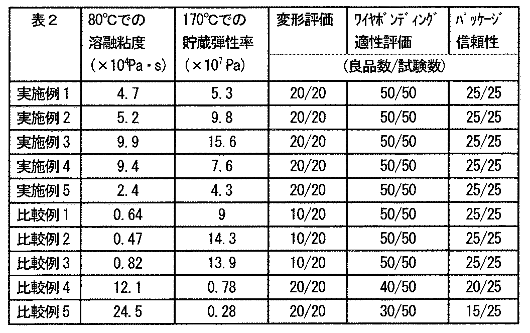
得られた接着シートを用いて<溶融粘度>、<貯蔵弾性率>、<パッケージ信頼性>、<接着剤層の変形>および<ワイヤボンディング適性>を評価した。結果を表2に示す。
本発明の接着剤組成物を用いることで、ダイシング時およびダイボンド時の接着剤層の変形を抑制しつつ、ワイヤボンディング適性を維持することができ、半導体パッケージの信頼性、歩留まりが向上することが確認できた。 By using the adhesive composition of the present invention, wire bonding suitability can be maintained while suppressing deformation of the adhesive layer during dicing and die bonding, and the reliability and yield of the semiconductor package can be improved. It could be confirmed.
Claims (4)
熱硬化前の接着剤組成物の80℃における溶融粘度が1.0×10⁴Pa・s以上であり、かつ、熱硬化後の接着剤組成物の170℃における貯蔵弾性率E’が1.0×10⁷Pa以上である接着用組成物。 An adhesive composition comprising an acrylic polymer (A), an epoxy thermosetting resin (B), and a thermosetting agent (C),
The melt viscosity at 80 ° C. of the adhesive composition before thermosetting is 1.0 × 10 4 Pa · s or more, and the storage elastic modulus E ′ at 170 ° C. of the adhesive composition after thermosetting is 1. An adhesive composition that is 0 × 10 7 Pa or more.
Priority Applications (1)
| Application Number | Priority Date | Filing Date | Title |
|---|---|---|---|
| JP2011028835A JP2012167174A (en) | 2011-02-14 | 2011-02-14 | Adhesive composition, adhesive sheet, and method of manufacturing semiconductor device |
Applications Claiming Priority (1)
| Application Number | Priority Date | Filing Date | Title |
|---|---|---|---|
| JP2011028835A JP2012167174A (en) | 2011-02-14 | 2011-02-14 | Adhesive composition, adhesive sheet, and method of manufacturing semiconductor device |
Publications (1)
| Publication Number | Publication Date |
|---|---|
| JP2012167174A true JP2012167174A (en) | 2012-09-06 |
Family
ID=46971627
Family Applications (1)
| Application Number | Title | Priority Date | Filing Date |
|---|---|---|---|
| JP2011028835A Pending JP2012167174A (en) | 2011-02-14 | 2011-02-14 | Adhesive composition, adhesive sheet, and method of manufacturing semiconductor device |
Country Status (1)
| Country | Link |
|---|---|
| JP (1) | JP2012167174A (en) |
Cited By (10)
| Publication number | Priority date | Publication date | Assignee | Title |
|---|---|---|---|---|
| JP2015140408A (en) * | 2014-01-29 | 2015-08-03 | 日立化成株式会社 | Adhesive composition, electronic member using the adhesive composition and manufacturing method of semiconductor device |
| WO2015115553A1 (en) * | 2014-01-29 | 2015-08-06 | 日立化成株式会社 | Adhesive composition, method for manufacturing semiconductor device using adhesive composition, and solid-state imaging element |
| JP2015229744A (en) * | 2014-06-06 | 2015-12-21 | 東亞合成株式会社 | Active energy ray-curable adhesive composition for plastic film or sheet |
| JP2016135856A (en) * | 2015-01-15 | 2016-07-28 | リンテック株式会社 | Adhesive composition, film adhesive and method for producing laminate |
| US9920227B2 (en) | 2014-01-29 | 2018-03-20 | Hitachi Chemical Company, Ltd. | Resin composition, method for manufacturing semiconductor device using resin composition, and solid-state imaging element |
| US10358580B2 (en) | 2014-01-29 | 2019-07-23 | Hitachi Chemical Company, Ltd. | Adhesive composition, resin cured product obtained from adhesive composition, method for manufacturing semiconductor device using adhesive composition, and solid-state imaging element |
| WO2020196156A1 (en) * | 2019-03-22 | 2020-10-01 | リンテック株式会社 | Film adhesive and sheet for semiconductor processing |
| US11174415B2 (en) | 2015-11-09 | 2021-11-16 | Nitto Denko Corporation | Adhesion method, adhesion-structure, and adhesion kit |
| JP2023148426A (en) * | 2022-03-30 | 2023-10-13 | リンテック株式会社 | Use of protective film-forming film, protective film-forming composite sheet, kit, and protective film-forming film |
| WO2024116451A1 (en) * | 2022-11-29 | 2024-06-06 | 株式会社レゾナック | Adhesive film, adhesive tape, adhesive tape with release film, semiconductor device manufacturing method and semiconductor device |
Citations (9)
| Publication number | Priority date | Publication date | Assignee | Title |
|---|---|---|---|---|
| JP2002265888A (en) * | 2001-03-15 | 2002-09-18 | Hitachi Chem Co Ltd | Adhesive film, use thereof, and method of manufacturing semiconductor device |
| JP2004043762A (en) * | 2001-08-27 | 2004-02-12 | Hitachi Chem Co Ltd | Adhesive sheet, semiconductor device and method of manufacturing the same |
| WO2005103180A1 (en) * | 2004-04-20 | 2005-11-03 | Hitachi Chemical Co., Ltd. | Adhesive sheet, semiconductor device and process for producing semiconductor device |
| JP2007270125A (en) * | 2006-03-08 | 2007-10-18 | Hitachi Chem Co Ltd | Adhesive sheet, integrated sheet, semiconductor device, and method for manufacturing semiconductor device |
| JP2009120830A (en) * | 2007-10-24 | 2009-06-04 | Hitachi Chem Co Ltd | Adhesive sheet, semiconductor device using the same, and manufacturing method thereof |
| JP2009135506A (en) * | 2008-12-17 | 2009-06-18 | Hitachi Chem Co Ltd | Adhesive film, use thereof, and method for manufacturing semiconductor device |
| JP2009267321A (en) * | 2008-04-04 | 2009-11-12 | Hitachi Chem Co Ltd | Adhesive sheet, one-piece sheet, semiconductor device, and method of manufacturing semiconductor device |
| JP2010182816A (en) * | 2009-02-04 | 2010-08-19 | Nitto Denko Corp | Thermoset die bond film |
| JP2011214006A (en) * | 2011-06-17 | 2011-10-27 | Hitachi Chem Co Ltd | Adhesive film, its application, and method for manufacturing semiconductor device |
-
2011
- 2011-02-14 JP JP2011028835A patent/JP2012167174A/en active Pending
Patent Citations (9)
| Publication number | Priority date | Publication date | Assignee | Title |
|---|---|---|---|---|
| JP2002265888A (en) * | 2001-03-15 | 2002-09-18 | Hitachi Chem Co Ltd | Adhesive film, use thereof, and method of manufacturing semiconductor device |
| JP2004043762A (en) * | 2001-08-27 | 2004-02-12 | Hitachi Chem Co Ltd | Adhesive sheet, semiconductor device and method of manufacturing the same |
| WO2005103180A1 (en) * | 2004-04-20 | 2005-11-03 | Hitachi Chemical Co., Ltd. | Adhesive sheet, semiconductor device and process for producing semiconductor device |
| JP2007270125A (en) * | 2006-03-08 | 2007-10-18 | Hitachi Chem Co Ltd | Adhesive sheet, integrated sheet, semiconductor device, and method for manufacturing semiconductor device |
| JP2009120830A (en) * | 2007-10-24 | 2009-06-04 | Hitachi Chem Co Ltd | Adhesive sheet, semiconductor device using the same, and manufacturing method thereof |
| JP2009267321A (en) * | 2008-04-04 | 2009-11-12 | Hitachi Chem Co Ltd | Adhesive sheet, one-piece sheet, semiconductor device, and method of manufacturing semiconductor device |
| JP2009135506A (en) * | 2008-12-17 | 2009-06-18 | Hitachi Chem Co Ltd | Adhesive film, use thereof, and method for manufacturing semiconductor device |
| JP2010182816A (en) * | 2009-02-04 | 2010-08-19 | Nitto Denko Corp | Thermoset die bond film |
| JP2011214006A (en) * | 2011-06-17 | 2011-10-27 | Hitachi Chem Co Ltd | Adhesive film, its application, and method for manufacturing semiconductor device |
Cited By (18)
| Publication number | Priority date | Publication date | Assignee | Title |
|---|---|---|---|---|
| US10808150B2 (en) | 2014-01-29 | 2020-10-20 | Hitachi Chemical Company, Ltd. | Resin composition, method for manufacturing semiconductor device using resin composition, and solid-state imaging element |
| WO2015115553A1 (en) * | 2014-01-29 | 2015-08-06 | 日立化成株式会社 | Adhesive composition, method for manufacturing semiconductor device using adhesive composition, and solid-state imaging element |
| JPWO2015115553A1 (en) * | 2014-01-29 | 2017-03-23 | 日立化成株式会社 | Adhesive composition, method for manufacturing semiconductor device using adhesive composition, and solid-state imaging device |
| US9868884B2 (en) | 2014-01-29 | 2018-01-16 | Hitachi Chemical Company, Ltd. | Adhesive composition, method for manufacturing semiconductor device using adhesive composition, and solid-state imaging element |
| US9920227B2 (en) | 2014-01-29 | 2018-03-20 | Hitachi Chemical Company, Ltd. | Resin composition, method for manufacturing semiconductor device using resin composition, and solid-state imaging element |
| US10358580B2 (en) | 2014-01-29 | 2019-07-23 | Hitachi Chemical Company, Ltd. | Adhesive composition, resin cured product obtained from adhesive composition, method for manufacturing semiconductor device using adhesive composition, and solid-state imaging element |
| JP2015140408A (en) * | 2014-01-29 | 2015-08-03 | 日立化成株式会社 | Adhesive composition, electronic member using the adhesive composition and manufacturing method of semiconductor device |
| JP2015229744A (en) * | 2014-06-06 | 2015-12-21 | 東亞合成株式会社 | Active energy ray-curable adhesive composition for plastic film or sheet |
| JP2016135856A (en) * | 2015-01-15 | 2016-07-28 | リンテック株式会社 | Adhesive composition, film adhesive and method for producing laminate |
| US11174415B2 (en) | 2015-11-09 | 2021-11-16 | Nitto Denko Corporation | Adhesion method, adhesion-structure, and adhesion kit |
| US11649379B2 (en) | 2015-11-09 | 2023-05-16 | Nitto Denko Corporation | Adhesion method, adhesion-structure, and adhesion kit |
| JPWO2020196156A1 (en) * | 2019-03-22 | 2020-10-01 | ||
| CN112930380A (en) * | 2019-03-22 | 2021-06-08 | 琳得科株式会社 | Film-like adhesive and sheet for semiconductor processing |
| WO2020196156A1 (en) * | 2019-03-22 | 2020-10-01 | リンテック株式会社 | Film adhesive and sheet for semiconductor processing |
| CN112930380B (en) * | 2019-03-22 | 2022-10-28 | 琳得科株式会社 | Film-like adhesive and sheet for semiconductor processing |
| JP7413356B2 (en) | 2019-03-22 | 2024-01-15 | リンテック株式会社 | Film adhesives and sheets for semiconductor processing |
| JP2023148426A (en) * | 2022-03-30 | 2023-10-13 | リンテック株式会社 | Use of protective film-forming film, protective film-forming composite sheet, kit, and protective film-forming film |
| WO2024116451A1 (en) * | 2022-11-29 | 2024-06-06 | 株式会社レゾナック | Adhesive film, adhesive tape, adhesive tape with release film, semiconductor device manufacturing method and semiconductor device |
Similar Documents
| Publication | Publication Date | Title |
|---|---|---|
| KR102143744B1 (en) | Composite sheet for resin film formation | |
| JP5917215B2 (en) | Adhesive composition, adhesive sheet, and method for manufacturing semiconductor device | |
| JP6393449B2 (en) | Adhesive composition, adhesive sheet, and method for manufacturing semiconductor device | |
| JP2012167174A (en) | Adhesive composition, adhesive sheet, and method of manufacturing semiconductor device | |
| JP6250265B2 (en) | Adhesive composition, adhesive sheet, and method for manufacturing semiconductor device | |
| JP5774322B2 (en) | Adhesive composition for semiconductor, adhesive sheet for semiconductor, and method for manufacturing semiconductor device | |
| JP5951207B2 (en) | Dicing die bonding sheet | |
| CN101275062A (en) | Adhesive composition, adhesive sheet, and method for producing semiconductor device | |
| JP6833083B2 (en) | Manufacturing method for film-like adhesives, adhesive sheets and semiconductor devices | |
| WO2014192745A1 (en) | Adhesive agent composition, adhesive sheet, and method for manufacturing semiconductor device | |
| JP2008231366A (en) | Pressure-sensitive adhesive composition, pressure-sensitive adhesive sheet, and method for manufacturing semiconductor device | |
| JP2010189485A (en) | Adhesive composition, adhesive sheet, and method for producing semiconductor device | |
| WO2013157567A1 (en) | Adhesive composition, adhesive sheet and method for manufacturing semiconductor device | |
| JP6029544B2 (en) | Adhesive composition, adhesive sheet, and method for manufacturing semiconductor device | |
| JP5237647B2 (en) | Adhesive composition, adhesive sheet and method for producing semiconductor device | |
| JP5662810B2 (en) | Adhesive composition, adhesive sheet, and method for manufacturing semiconductor device | |
| JP5513734B2 (en) | Adhesive composition, adhesive sheet, and method for manufacturing semiconductor device | |
| JP5414256B2 (en) | Adhesive composition, adhesive sheet, and method for manufacturing semiconductor device | |
| JP5005258B2 (en) | Adhesive composition, adhesive sheet and method for producing semiconductor device | |
| JP6279319B2 (en) | Composite sheet for resin film formation | |
| JP2010189484A (en) | Adhesive composition, adhesive sheet and method for manufacturing semiconductor device | |
| JP5005325B2 (en) | Adhesive composition, adhesive sheet and method for producing semiconductor device | |
| JP5727811B2 (en) | Semiconductor chip pickup method and semiconductor device manufacturing method | |
| JP6029536B2 (en) | Adhesive composition, adhesive sheet, and method for manufacturing semiconductor device | |
| JP2009227892A (en) | Tacky adhesive composition, tacky adhesive sheet, and method for producing semiconductor device |
Legal Events
| Date | Code | Title | Description |
|---|---|---|---|
| A621 | Written request for application examination |
Free format text: JAPANESE INTERMEDIATE CODE: A621 Effective date: 20131008 |
|
| RD02 | Notification of acceptance of power of attorney |
Free format text: JAPANESE INTERMEDIATE CODE: A7422 Effective date: 20131008 |
|
| A977 | Report on retrieval |
Free format text: JAPANESE INTERMEDIATE CODE: A971007 Effective date: 20140519 |
|
| A131 | Notification of reasons for refusal |
Free format text: JAPANESE INTERMEDIATE CODE: A131 Effective date: 20140527 |
|
| A521 | Request for written amendment filed |
Free format text: JAPANESE INTERMEDIATE CODE: A523 Effective date: 20140725 |
|
| A02 | Decision of refusal |
Free format text: JAPANESE INTERMEDIATE CODE: A02 Effective date: 20150120 |