JP2012159448A - Defect inspection method and manufacturing method of semiconductor device - Google Patents
Defect inspection method and manufacturing method of semiconductor device Download PDFInfo
- Publication number
- JP2012159448A JP2012159448A JP2011020375A JP2011020375A JP2012159448A JP 2012159448 A JP2012159448 A JP 2012159448A JP 2011020375 A JP2011020375 A JP 2011020375A JP 2011020375 A JP2011020375 A JP 2011020375A JP 2012159448 A JP2012159448 A JP 2012159448A
- Authority
- JP
- Japan
- Prior art keywords
- electrode
- conductive layer
- imprint pattern
- shot
- defect
- Prior art date
- Legal status (The legal status is an assumption and is not a legal conclusion. Google has not performed a legal analysis and makes no representation as to the accuracy of the status listed.)
- Abandoned
Links
- 230000007547 defect Effects 0.000 title claims abstract description 88
- 238000007689 inspection Methods 0.000 title claims abstract description 68
- 238000000034 method Methods 0.000 title claims description 69
- 239000004065 semiconductor Substances 0.000 title description 6
- 238000004519 manufacturing process Methods 0.000 title description 5
- 239000008151 electrolyte solution Substances 0.000 claims abstract description 38
- 238000005259 measurement Methods 0.000 claims abstract description 7
- 239000003792 electrolyte Substances 0.000 claims description 8
- 238000012545 processing Methods 0.000 claims description 3
- 239000000243 solution Substances 0.000 abstract description 2
- 239000010410 layer Substances 0.000 description 40
- 239000000463 material Substances 0.000 description 12
- 239000000758 substrate Substances 0.000 description 9
- 230000002950 deficient Effects 0.000 description 6
- 239000011248 coating agent Substances 0.000 description 5
- 238000000576 coating method Methods 0.000 description 5
- 229910052751 metal Inorganic materials 0.000 description 4
- 239000002184 metal Substances 0.000 description 4
- HEMHJVSKTPXQMS-UHFFFAOYSA-M Sodium hydroxide Chemical compound [OH-].[Na+] HEMHJVSKTPXQMS-UHFFFAOYSA-M 0.000 description 3
- 239000012790 adhesive layer Substances 0.000 description 3
- 239000012212 insulator Substances 0.000 description 3
- 238000012544 monitoring process Methods 0.000 description 3
- 239000004020 conductor Substances 0.000 description 2
- 229910052802 copper Inorganic materials 0.000 description 2
- 239000000428 dust Substances 0.000 description 2
- 238000003825 pressing Methods 0.000 description 2
- 238000004904 shortening Methods 0.000 description 2
- 239000000853 adhesive Substances 0.000 description 1
- 230000001070 adhesive effect Effects 0.000 description 1
- 238000001035 drying Methods 0.000 description 1
- 239000010419 fine particle Substances 0.000 description 1
- -1 for example Substances 0.000 description 1
- 230000006870 function Effects 0.000 description 1
- 239000011521 glass Substances 0.000 description 1
- 239000011229 interlayer Substances 0.000 description 1
- 238000005468 ion implantation Methods 0.000 description 1
- 230000001678 irradiating effect Effects 0.000 description 1
- 238000012986 modification Methods 0.000 description 1
- 230000004048 modification Effects 0.000 description 1
- 230000002093 peripheral effect Effects 0.000 description 1
- 239000010453 quartz Substances 0.000 description 1
- 239000011347 resin Substances 0.000 description 1
- 229920005989 resin Polymers 0.000 description 1
- 239000000523 sample Substances 0.000 description 1
- VYPSYNLAJGMNEJ-UHFFFAOYSA-N silicon dioxide Inorganic materials O=[Si]=O VYPSYNLAJGMNEJ-UHFFFAOYSA-N 0.000 description 1
- 238000004528 spin coating Methods 0.000 description 1
- 238000004544 sputter deposition Methods 0.000 description 1
- 229920001187 thermosetting polymer Polymers 0.000 description 1
- 238000013518 transcription Methods 0.000 description 1
- 230000035897 transcription Effects 0.000 description 1
- 238000012546 transfer Methods 0.000 description 1
Images


Classifications
-
- H—ELECTRICITY
- H01—ELECTRIC ELEMENTS
- H01L—SEMICONDUCTOR DEVICES NOT COVERED BY CLASS H10
- H01L22/00—Testing or measuring during manufacture or treatment; Reliability measurements, i.e. testing of parts without further processing to modify the parts as such; Structural arrangements therefor
- H01L22/10—Measuring as part of the manufacturing process
- H01L22/12—Measuring as part of the manufacturing process for structural parameters, e.g. thickness, line width, refractive index, temperature, warp, bond strength, defects, optical inspection, electrical measurement of structural dimensions, metallurgic measurement of diffusions
-
- B—PERFORMING OPERATIONS; TRANSPORTING
- B82—NANOTECHNOLOGY
- B82Y—SPECIFIC USES OR APPLICATIONS OF NANOSTRUCTURES; MEASUREMENT OR ANALYSIS OF NANOSTRUCTURES; MANUFACTURE OR TREATMENT OF NANOSTRUCTURES
- B82Y10/00—Nanotechnology for information processing, storage or transmission, e.g. quantum computing or single electron logic
-
- B—PERFORMING OPERATIONS; TRANSPORTING
- B82—NANOTECHNOLOGY
- B82Y—SPECIFIC USES OR APPLICATIONS OF NANOSTRUCTURES; MEASUREMENT OR ANALYSIS OF NANOSTRUCTURES; MANUFACTURE OR TREATMENT OF NANOSTRUCTURES
- B82Y40/00—Manufacture or treatment of nanostructures
-
- G—PHYSICS
- G03—PHOTOGRAPHY; CINEMATOGRAPHY; ANALOGOUS TECHNIQUES USING WAVES OTHER THAN OPTICAL WAVES; ELECTROGRAPHY; HOLOGRAPHY
- G03F—PHOTOMECHANICAL PRODUCTION OF TEXTURED OR PATTERNED SURFACES, e.g. FOR PRINTING, FOR PROCESSING OF SEMICONDUCTOR DEVICES; MATERIALS THEREFOR; ORIGINALS THEREFOR; APPARATUS SPECIALLY ADAPTED THEREFOR
- G03F7/00—Photomechanical, e.g. photolithographic, production of textured or patterned surfaces, e.g. printing surfaces; Materials therefor, e.g. comprising photoresists; Apparatus specially adapted therefor
- G03F7/0002—Lithographic processes using patterning methods other than those involving the exposure to radiation, e.g. by stamping
-
- G—PHYSICS
- G03—PHOTOGRAPHY; CINEMATOGRAPHY; ANALOGOUS TECHNIQUES USING WAVES OTHER THAN OPTICAL WAVES; ELECTROGRAPHY; HOLOGRAPHY
- G03F—PHOTOMECHANICAL PRODUCTION OF TEXTURED OR PATTERNED SURFACES, e.g. FOR PRINTING, FOR PROCESSING OF SEMICONDUCTOR DEVICES; MATERIALS THEREFOR; ORIGINALS THEREFOR; APPARATUS SPECIALLY ADAPTED THEREFOR
- G03F9/00—Registration or positioning of originals, masks, frames, photographic sheets or textured or patterned surfaces, e.g. automatically
- G03F9/70—Registration or positioning of originals, masks, frames, photographic sheets or textured or patterned surfaces, e.g. automatically for microlithography
- G03F9/7003—Alignment type or strategy, e.g. leveling, global alignment
- G03F9/7007—Alignment other than original with workpiece
- G03F9/7011—Pre-exposure scan; original with original holder alignment; Prealignment, i.e. workpiece with workpiece holder
-
- H—ELECTRICITY
- H01—ELECTRIC ELEMENTS
- H01L—SEMICONDUCTOR DEVICES NOT COVERED BY CLASS H10
- H01L22/00—Testing or measuring during manufacture or treatment; Reliability measurements, i.e. testing of parts without further processing to modify the parts as such; Structural arrangements therefor
- H01L22/10—Measuring as part of the manufacturing process
- H01L22/14—Measuring as part of the manufacturing process for electrical parameters, e.g. resistance, deep-levels, CV, diffusions by electrical means
Abstract
Description
本発明の実施形態は欠陥検査方法および半導体装置の製造方法に関する。 FIELD Embodiments described herein relate generally to a defect inspection method and a semiconductor device manufacturing method.
半導体装置の製造工程において被転写基板に原版の型を転写するナノインプリント露光法が注目されている。ナノインプリント法は、転写されるパターンが形成された原版の型(テンプレート)を、基板上に塗布されているインプリント材料からなるレジスト層に押し付け、レジスト層を硬化させることにより、レジスト層にパターンを転写する方法である。 Attention has been focused on a nanoimprint exposure method in which a master mold is transferred to a substrate to be transferred in a manufacturing process of a semiconductor device. In the nanoimprint method, an original mold (template) on which a pattern to be transferred is formed is pressed against a resist layer made of an imprint material applied on a substrate, and the resist layer is cured to form a pattern on the resist layer. It is a method of transcription.
このナノインプリントのパターン形成方法は、テンプレートとウェハが密着してインプリントされるため、テンプレートの破損や欠陥が突発的に発生する。このようなテンプレートの破損や欠陥を放置したままインプリント処理を継続すると、大量の不良品が発生するため、テンプレートの破損や欠陥を早期に発見することが望まれる。 In this nanoimprint pattern forming method, since the template and the wafer are imprinted in close contact with each other, the template is suddenly damaged or defective. If the imprint process is continued while leaving such a template breakage or defect, a large number of defective products are generated. Therefore, it is desired to find the template breakage or defect at an early stage.
本発明の一つの実施形態の目的は、インプリントパターンの欠陥の有無の検査を効率化することが可能な欠陥検査方法および半導体装置の製造方法を提供することである。 An object of one embodiment of the present invention is to provide a defect inspection method and a semiconductor device manufacturing method capable of improving the efficiency of inspection for the presence or absence of imprint pattern defects.
実施形態の欠陥検査方法によれば、下地層上に導電層を形成する。次に、前記導電層上にインプリントパターンを形成する。次に、前記インプリントパターンに電解液を接触させる。次に、前記電解液に電極を接触させる。次に、前記導電層と前記電極との間に電圧を印加する。次に、前記導電層と前記電極との間に電圧が印加された時に前記導電層と前記電極との間に流れる電流を計測する。次に、前記電流の計測結果に基づいて前記インプリントパターンの欠陥の有無を判定する。 According to the defect inspection method of the embodiment, the conductive layer is formed on the base layer. Next, an imprint pattern is formed on the conductive layer. Next, an electrolytic solution is brought into contact with the imprint pattern. Next, an electrode is brought into contact with the electrolytic solution. Next, a voltage is applied between the conductive layer and the electrode. Next, a current flowing between the conductive layer and the electrode is measured when a voltage is applied between the conductive layer and the electrode. Next, the presence or absence of a defect in the imprint pattern is determined based on the measurement result of the current.
以下、実施形態に係る欠陥検査方法について図面を参照しながら説明する。なお、これらの実施形態により本発明が限定されるものではない。 Hereinafter, a defect inspection method according to an embodiment will be described with reference to the drawings. Note that the present invention is not limited to these embodiments.
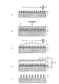
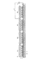
(第1実施形態)
図1は、第1実施形態に係る欠陥検査方法の概略構成を示す断面図である。
図1(a)において、下地層1上に導電層2を形成する。なお、下地層1としては、例えば、半導体基板を用いることができる。あるいは、下地層1は、半導体基板上の絶縁層であってもよいし、絶縁層上の導電層であってもよい。導電層2としては、例えば、レジストパターンの接着強度を上げる接着層に導電体を混入した膜を用いることができる。この接着層としては、例えば、low−k(低誘電率)膜等の層間絶縁膜または有機膜を用いることができる。接着層に混入される導電体としては、例えば、金属微粒子を用いることができる。また、導電層2の形成方法としては、スピンコートなどを用いるようにしてもよい。あるいは、下地層1との密着性が確保できるならば、金属のスパッタなどの方法にて導電層2を形成するようにしてもよい。
(First embodiment)
FIG. 1 is a cross-sectional view showing a schematic configuration of the defect inspection method according to the first embodiment.
In FIG. 1A, a
次に、インクジェット法などの方法を用いることにより、ノズル3を介してインプリント材4´を導電層2上に吐出させる。なお、インプリント材4´としては、例えば、紫外線硬化型レジストを用いることができる。また、インプリント材4´は、絶縁体にて構成することができる。
Next, the
次に、図1(b)に示すように、テンプレート5をインプリント材4´に押し当てることにより、導電層2上にインプリントパターン4を形成する。なお、テンプレート5は、例えば、石英にて構成することができる。ここで、テンプレート5には、インプリントパターン4に対応した凹部5aが形成されている。そして、テンプレート5をインプリント材4´に押し当てると、毛細管現象によってインプリント材4´が凹部5aに吸い上げられ、凹部5aの形状に対応したインプリントパターン4が形成される。
Next, as shown in FIG. 1B, the
そして、テンプレート5をインプリントパターン4に押し当てたまま、テンプレート5を通して紫外線をインプリントパターン4に照射することにより、インプリントパターン4を硬化させる。
Then, the
なお、図1(b)の例では、インプリントパターン4を硬化させるために、インプリント材4´として紫外線硬化型レジストを用いるようにしてもよいが、熱硬化型レジストを用いるようにしてもよい。
In the example of FIG. 1B, an ultraviolet curable resist may be used as the
次に、図1(c)に示すように、テンプレート5をインプリントパターン4から除去した後、インクジェット法などの方法を用いることにより、ノズル3を介して電解液6をインプリントパターン4上に吐出させる。なお、電解液6としては、例えば、水酸化ナトリウム溶液を用いることができる。
Next, as shown in FIG. 1C, after removing the template 5 from the
次に、図1(d)に示すように、電解液6に電極7を接触させるとともに、導電層2に電極8を接触させる。なお、電極7、8は、プローブ電極であってもよいし、プレート電極であってもよい。また、電極7、8は、CuやAlなどの金属を用いることができる。
Next, as shown in FIG. 1 (d), the
そして、電源9を介して電極7、8間に電圧を印加し、その時に電極7、8間に流れる電流を電流計10にて計測する。この時、インプリントパターン4は絶縁体にて構成されているので、インプリントパターン4に欠陥が無い時は電極7、8間に電流は流れない。
Then, a voltage is applied between the
そして、電流計10にて計測された電流の計測値をしきい値と比較し、その計測値がしきい値以下の場合、インプリントパターン4に欠陥が無いと判定する。
Then, the measured value of the current measured by the
次に、図1(e)に示すように、電解液6および電極7をインプリントパターン4上から除去するとともに、電極8を導電層2から除去する。なお、電解液6をインプリントパターン4上から除去する方法としては、自然乾燥であってもよいし、ブロワー処理を行うようにしてもよい。また、電解液6をインプリントパターン4上から除去した後、インプリントパターン4の表面を洗浄するようにしてもよい。
Next, as shown in FIG. 1 (e), the
そして、インプリントパターン4の欠陥が無いと判定された場合、インプリントパターン4を介して下地層1を処理する。なお、下地層1の処理としては、インプリントパターン4を介して下地層1にイオン注入を行うようにしてもよいし、インプリントパターン4をマスクとして下地層1をエッチングするようにしてもよい。その後、下地層1上に残った導電層2およびインプリントパターン4を除去する。
When it is determined that there is no defect in the
図2は、第1実施形態に係るテンプレートの欠陥がある時の欠陥検査方法を示す断面図である。
図2(a)において、図1(a)と同様に、下地層1上に導電層2を形成した後、ノズル3を介してインプリント材4´を導電層2上に吐出させる。
FIG. 2 is a cross-sectional view showing a defect inspection method when there is a template defect according to the first embodiment.
In FIG. 2A, as in FIG. 1A, the
次に、図2(b)に示すように、テンプレート5をインプリント材4´に押し当てることにより、導電層2上にインプリントパターン4を形成する。この時、テンプレート5の表面に塵などの異物11が付着している場合、異物11もインプリントパターン4に転写され、インプリントパターン4に欠陥12が発生する。
Next, as shown in FIG. 2B, the
なお、インプリントパターン4の欠陥12の発生原因としては、例えば、レジストの充填不良(ダスト、離形時のレジスト剥がれ)、気泡、微小泡、インクジェットバブル、テンプレート凹部異物詰まりおよびウェハ基板上の異物などを挙げることができる。
Note that the
次に、図2(c)に示すように、テンプレート5をインプリントパターン4から除去した後、ノズル3を介して電解液6をインプリントパターン4上に吐出させる。この時、電解液6は欠陥12に入り込み、導電層2と接触する。
Next, as shown in FIG. 2C, after removing the template 5 from the
次に、図2(d)に示すように、電解液6に電極7を接触させるとともに、導電層2に電極8を接触させる。そして、電源9を介して電極7、8間に電圧を印加し、その時に電極7、8間に流れる電流を電流計10にて計測する。この時、電解液6は欠陥12を介して導電層2と接触するので、電流パスPAを介して電極7、8間に電流が流れる。そして、電流計10にて計測された電流の計測値をしきい値と比較し、その計測値がしきい値を超える場合、インプリントパターン4に欠陥が有ると判定する。
Next, as shown in FIG. 2 (d), the
ここで、インプリントパターン4に欠陥が有ると判定された場合、それ以降の工程を止めることにより、大量の不良品が発生するのを防止することができる。
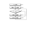
図3は、第1実施形態に係る欠陥検査方法を示すフローチャートである。
図3において、インプリントパターンが形成されたウェハ上の検査領域を指定する(S1)。なお、検査領域は検査レシピにて設定することができる。
Here, when it is determined that the
FIG. 3 is a flowchart showing the defect inspection method according to the first embodiment.
In FIG. 3, the inspection area on the wafer on which the imprint pattern is formed is designated (S1). The inspection area can be set by an inspection recipe.
次に、インクジェット法にて検査領域上に電解液を塗布する(S2)。なお、インクジェット法では、検査領域を1滴分の面積ごとに指定することができ、例えば、1滴分の面積は20μmΦとすることができる。 Next, an electrolytic solution is applied on the inspection region by the ink jet method (S2). In the inkjet method, the inspection region can be specified for each area of one drop, and for example, the area of one drop can be set to 20 μmΦ.
次に、電極用テンプレート対極を準備し(S3)、テンプレート電極と対極間に電圧を印加する(S4)。 Next, an electrode template counter electrode is prepared (S3), and a voltage is applied between the template electrode and the counter electrode (S4).
次に、テンプレート電極を電解液上に設置し(S5)、テンプレート電極と対極との間の電流をモニタする(S6)。テンプレート電極は、その自重のみで電解液上に設置するようにしてもよい。テンプレート電極と対極との間の電流のモニタ結果に基づいてインプリントパターンの欠陥の有無を判定する(S7)。 Next, the template electrode is placed on the electrolytic solution (S5), and the current between the template electrode and the counter electrode is monitored (S6). You may make it install a template electrode on electrolyte solution only with the dead weight. Based on the result of monitoring the current between the template electrode and the counter electrode, the presence or absence of imprint pattern defects is determined (S7).
(第2実施形態)
図4は、第2実施形態に係る欠陥検査方法を示す断面図である。
図4において、ウェハW上には導電層2を介してインプリントパターン4がショット領域Sh1〜Sh4ごとに形成されている。そして、インクジェット法にて電解液6をショット領域Sh1〜Sh4ごとに塗布する。
(Second Embodiment)
FIG. 4 is a cross-sectional view illustrating the defect inspection method according to the second embodiment.
In FIG. 4, an
そして、ショット領域Sh1〜Sh4ごとに電極7を移動させながら、電極7を電解液6に接触させることにより、ショット領域Sh1〜Sh4ごとに電極7、8間に流れる電流を電流計10にて計測する。そして、電流計10にて計測された電流の計測値をショット領域Sh1〜Sh4ごとにしきい値と比較することにより、インプリントパターン4の欠陥の有無をショット領域Sh1〜Sh4ごとに判定する。
Then, while the
これにより、インプリントパターン4の欠陥の有無をショット領域Sh1〜Sh4ごとに特定することが可能となり、インプリントパターン4の欠陥の発生原因の解明を容易化することができる。
Accordingly, it is possible to specify the presence or absence of defects in the
図5は、第2実施形態に係る欠陥検査方法を示す平面図である。
図5において、ウェハWはショット領域Shごとに区画されている。そして、インクジェット法にて電解液をショット領域Shごとに塗布した後、ショット領域Shごとに電流リークをモニタすることで、欠陥の有無をショット領域Shごとに判定することができる。
FIG. 5 is a plan view showing the defect inspection method according to the second embodiment.
In FIG. 5, the wafer W is partitioned for each shot area Sh. And after apply | coating electrolyte solution for every shot area | region Sh with the inkjet method, the presence or absence of a defect can be determined for every shot area | region Sh by monitoring a current leak for every shot area | region Sh.
図6は、第2実施形態に係る欠陥検査方法のショット位置と電流との関係を示す平面図である。
図6において、各ショット領域Shごとに電流リーク量IRがしきい値LHと比較される。そして、電流リーク量IRがしきい値LH以下のショット領域Shについては欠陥がないと判定され、電流リーク量IRがしきい値LHを越えるショット領域Shについては欠陥があると判定される。
FIG. 6 is a plan view showing the relationship between the shot position and the current in the defect inspection method according to the second embodiment.
In FIG. 6, the current leak amount IR is compared with the threshold value LH for each shot region Sh. Then, it is determined that there is no defect in the shot region Sh where the current leak amount IR is equal to or less than the threshold value LH, and it is determined that there is a defect in the shot region Sh where the current leak amount IR exceeds the threshold value LH.
図7は、第2実施形態に係る欠陥検査方法を示すフローチャートである。
図7において、ショット検査が行われるものとすると(S11)、ショット領域Shごとに電流リークがモニタされる(S12)。そして、電流リーク量がしきい値LHを越える場合(S13)、そのショット領域Shが欠陥ショットとして登録された後(S14)、次のショット領域Shが検査される(S15)。
FIG. 7 is a flowchart showing the defect inspection method according to the second embodiment.
In FIG. 7, when a shot inspection is performed (S11), current leakage is monitored for each shot region Sh (S12). If the current leak amount exceeds the threshold LH (S13), the shot area Sh is registered as a defective shot (S14), and then the next shot area Sh is inspected (S15).
(第3実施形態)
図8は、第3実施形態に係る欠陥検査方法を示す断面図である。
図8において、ウェハW上には導電層2を介してインプリントパターン4がショット領域Sh1〜Sh4ごとに形成されている。そして、インクジェット法にて電解液6をショット領域Sh1〜Sh4ごとに塗布する。この時、電解液6は、各ショット領域Sh1〜Sh4の一部に選択的に塗布される。例えば、NAND型フラッシュメモリにおいてセル領域と周辺回路領域とで別個に電解液6を塗布することができる。
(Third embodiment)
FIG. 8 is a cross-sectional view illustrating the defect inspection method according to the third embodiment.
In FIG. 8, an
そして、ショット領域Sh1〜Sh4ごとに電極7を移動させながら、電極7を電解液6に接触させることにより、ショット領域Sh1〜Sh4ごとに電極7、8間に流れる電流を電流計10にて計測する。そして、電流計10にて計測された電流の計測値をショット領域Sh1〜Sh4ごとにしきい値と比較することにより、インプリントパターン4の特定の部分の欠陥の有無をショット領域Sh1〜Sh4ごとに判定する。
Then, while the
これにより、インプリントパターン4の欠陥の有無を回路機能ごとに特定することが可能となり、インプリントパターン4の欠陥の発生原因の解明を容易化することができる。
As a result, it is possible to specify the presence or absence of a defect in the
例えば、図4の方法でインプリントパターン4の欠陥検査を行い、その欠陥検査で欠陥の有ったショット領域Sh1〜Sh4を対象として電解液6を塗布する領域を狭くすることにより、インプリントパターン4の欠陥の発生位置を絞り込むことができる。
For example, the
図9は、第3実施形態に係る欠陥検査方法を示す平面図である。
図9において、ウェハWはショット領域Shごとに区画されている。また、各ショット領域Shは、チップ領域CP1〜CP4ごとに区画されている。そして、インクジェット法にて電解液6をチップ領域CP1の一部のみにショット領域Shごとに塗布した後、ショット領域Shごとに電流リークをモニタすることで、欠陥の有無をショット領域Shの特定の部分ごとに判定することができる。
FIG. 9 is a plan view showing the defect inspection method according to the third embodiment.
In FIG. 9, the wafer W is partitioned for each shot area Sh. Each shot area Sh is divided into chip areas CP1 to CP4. And after apply | coating the
(第4実施形態)
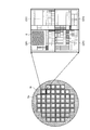
図10は、第4実施形態に係る欠陥検査装置の概略構成を示す平面図である。
図10において、インプリント装置21には、ウェハWの温度を調整するウェハ温調ステージ22、ウェハWの搬送位置を調整するプリアライメントステージ23、ウェハWを一時的に退避させる退避ステージ24、インプリント処理されるウェハWが配置されるn(nは2以上の整数)個のインプリントステージ25−1〜25−n、インライン検査されるウェハWが配置されるインライン検査ステージ26、インライン検査ステージ26上に配置されたウェハWをインライン検査するインライン検査装置27およびインライン検査結果に基づいてインプリント装置21の制御を行う制御装置28が設けられている。
(Fourth embodiment)
FIG. 10 is a plan view showing a schematic configuration of the defect inspection apparatus according to the fourth embodiment.
In FIG. 10, an
なお、インプリントステージ25−1〜25−nには、図1(a)のノズル3および図1(b)のテンプレート5および紫外線照射装置を個別に設けることができる。また、インライン検査ステージ26には、図1(d)のノズル3、電極7、8、電源9および電流計10を設けることができる。
The imprint stages 25-1 to 25-n can be individually provided with the nozzle 3 in FIG. 1A, the template 5 in FIG. 1B, and the ultraviolet irradiation device. Further, the
そして、導電層2が形成されたウェハWがウェハ温調ステージ22に搬送され、ウェハWの温度調節が行われた後、プリアライメントステージ23に搬送される。そして、プリアライメントステージ23を介してインプリントステージ25−1〜25−nのうちの空いているステージにウェハWが搬送され、ウェハWのインプリント処理が行われることで、導電層2上にインプリントパターン4が形成されるとともに、インプリントステージ25−1〜25−nのうちのインプリント処理が終わったステージからウェハWが搬出され、インライン検査ステージ26に搬入される。そして、インライン検査ステージ26においてインライン検査が行われ、導電層2上のインプリントパターン4の電流リークがモニタされる。
そして、インライン検査が終了したウェハWは、インライン検査ステージ26から搬出され、インプリントステージ25−1〜25−nへのウェハWの搬入の妨げになる場合は、プリアライメントステージ23を介して退避ステージ24に一時的に退避される。
Then, the wafer W on which the
Then, the wafer W that has been subjected to the inline inspection is unloaded from the
また、インライン検査装置27において、電流リーク量に基づいてインプリントパターン4の欠陥の有無が判定され、ウェハWごとに欠陥の有無が登録される。そして、制御装置28において、欠陥の有ったウェハWのインプリント処理が行われたインプリントステージ25−1〜25−nが特定され、そのインプリントステージ25−1〜25−nの使用が停止される。
Further, the
これにより、複数のインプリントステージ25−1〜25−nに対して1台のインライン検査ステージ26を共用させることができ、インライン検査ステージ26の稼働率を向上させることが可能となるとともに、インプリント処理後の待機時間を短くしつつインライン検査を行うことができ、量産時に不良品が大量に発生する危険性を減らすことができる。
As a result, one
(第5実施形態)
図11は、第5実施形態に係る欠陥検査方法を示す断面図である。
図11において、この欠陥検査方法では、図4の電極7の代わりに電極31が用いられている。なお、電極7は、1つのショット領域の電解液に接触されるのに対し、電極31は、ウェハW上の複数のショット領域Sh1〜Sh4に一括して接触される。例えば、ウェハW上の全てのショット領域Sh1〜Sh4に一括して接触できるようにするため、電極31の形状は、例えば、ウェハWと同様の形状に設定することができる。
(Fifth embodiment)
FIG. 11 is a cross-sectional view illustrating the defect inspection method according to the fifth embodiment.
11, in this defect inspection method, an
そして、インクジェット法にて電解液6をショット領域Sh1〜Sh4ごとに塗布した後、複数のショット領域Sh1〜Sh4の電解液6に電極31を一括して接触させることにより、電極31、8間に流れる電流を電流計10にて計測する。そして、電流計10にて計測された電流の計測値をしきい値と比較することにより、インプリントパターン4の欠陥の有無を複数のショット領域Sh1〜Sh4について一括して判定する。
And after apply | coating the
これにより、1回の電流計測処理によって、インプリントパターン4の欠陥の有無を複数のショット領域Sh1〜Sh4について判定することが可能となり、欠陥検査処理にかかる時間を短縮することができる。
Accordingly, it is possible to determine the presence or absence of defects in the
(第6実施形態)
図12は、第6実施形態に係る欠陥検査方法を示す断面図である。
図11の欠陥検査方法では、ショット領域Sh1〜Sh4ごとにインプリントパターン4が分離されているのに対し、図12の欠陥検査方法では、ショット領域Sh1〜Sh4に渡ってインプリントパターン4が連続して形成され、ショット領域Sh1〜Sh4間で導電層2がインプリントパターン4から露出しないようにされている。
(Sixth embodiment)
FIG. 12 is a cross-sectional view illustrating the defect inspection method according to the sixth embodiment.
In the defect inspection method of FIG. 11, the
そして、インクジェット法にて電解液6をショット領域Sh1〜Sh4に渡って連続して塗布した後、その電解液6に電極31を接触させることにより、電極31、8間に流れる電流を電流計10にて計測する。そして、電流計10にて計測された電流の計測値をしきい値と比較することにより、インプリントパターン4の欠陥の有無を複数のショット領域Sh1〜Sh4について一括して判定する。
And after apply | coating the
これにより、電解液6をショット領域Sh1〜Sh4ごとに分離することなく、1回の電流計測処理によって、インプリントパターン4の欠陥の有無を複数のショット領域Sh1〜Sh4について判定することが可能となり、欠陥検査処理にかかる時間を短縮することができる。
This makes it possible to determine the presence or absence of defects in the
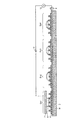
(第7実施形態)
図13は、第7実施形態に係る欠陥検査方法を示す断面図である。
図13において、この欠陥検査方法では、図11の電極31の代わりに電極31−1〜31−4が用いられている。そして、電極31−1〜31−4は支持基板32にて支持されている。なお、支持基板32としては、例えば、ガラスや樹脂などの絶縁体を用いることができる。また、電極31−1〜31−4としては、例えば、CuやAlなどの金属膜を用いることができる。また、電極31は、ウェハW上の複数のショット領域Sh1〜Sh4に一括して接触されるのに対し、電極31−1〜31−4は、ショット領域Sh1〜Sh4の電解液にそれぞれ接触される。また、電極31−1〜31−4がウェハW上の全てのショット領域Sh1〜Sh4にそれぞれ一括して接触できるようにするため、支持基板32の形状は、例えば、ウェハWと同様の形状に設定することができる。そして、電極31−1〜31−4は、切替部34を介して電源9に接続されている。なお、切替部34は、電極31−1〜31−4のうちのいずれか1個の電極を選択して電源9に接続することができる。
(Seventh embodiment)
FIG. 13 is a cross-sectional view showing the defect inspection method according to the seventh embodiment.
13, in this defect inspection method, electrodes 31-1 to 31-4 are used instead of the
そして、インクジェット法にて電解液6をショット領域Sh1〜Sh4ごとに塗布した後、ショット領域Sh1〜Sh4の電解液6に電極31−1〜31−4をそれぞれ接触させる。そして、切替部34にて電極31−1〜31−4を順次切り替えさせながら、各電極31−1〜31−4と電極8との間に流れる電流を電流計10にて計測する。そして、電流計10にて計測された各電流の計測値をしきい値と比較することにより、インプリントパターン4の欠陥の有無をショット領域Sh1〜Sh4ごとに判定する。
And after apply | coating the
これにより、電極31−1〜31−4の位置を固定したまま、インプリントパターン4の欠陥の有無をショット領域Sh1〜Sh4ごとに特定することが可能となり、処理にかかる時間を短縮しつつ、インプリントパターン4の欠陥の発生原因の解明を容易化することができる。
This makes it possible to specify the presence or absence of defects in the
本発明のいくつかの実施形態を説明したが、これらの実施形態は、例として提示したものであり、発明の範囲を限定することは意図していない。これら新規な実施形態は、その他の様々な形態で実施されることが可能であり、発明の要旨を逸脱しない範囲で、種々の省略、置き換え、変更を行うことができる。これら実施形態やその変形は、発明の範囲や要旨に含まれるとともに、特許請求の範囲に記載された発明とその均等の範囲に含まれる。 Although several embodiments of the present invention have been described, these embodiments are presented by way of example and are not intended to limit the scope of the invention. These novel embodiments can be implemented in various other forms, and various omissions, replacements, and changes can be made without departing from the scope of the invention. These embodiments and modifications thereof are included in the scope and gist of the invention, and are included in the invention described in the claims and the equivalents thereof.
1 下地層、2 導電層、3 ノズル、4´ インプリント材、4 インプリントパターン、5 テンプレート、6 電解液、7、8、31、31−1〜31−4 電極、9 電源 10 電流計、11 異物、12 欠陥、Sh、Sh1〜Sh4 ショット領域、CP1〜CP4 チップ領域、21 インプリント装置、22 ウェハ温調ステージ、23 プリアライメントステージ、24 退避ステージ、25−1〜25−n インプリントステージ、26 インライン検査ステージ、27 インライン検査装置、28 制御装置、32 支持基板、34 切替部
DESCRIPTION OF
Claims (6)
前記導電層上にインプリントパターンを形成するステップと、
前記インプリントパターンに電解液を接触させるステップと、
前記電解液に電極を接触させるステップと、
前記導電層と前記電極との間に電圧を印加するステップと、
前記導電層と前記電極との間に電圧が印加された時に前記導電層と前記電極との間に流れる電流を計測するステップと、
前記電流の計測結果に基づいて前記インプリントパターンの欠陥の有無を判定するステップとを備え、
前記インプリントパターン上に前記電解液を選択的に吐出させ、前記電解液をショット単位または前記ショット内の一部の領域に吐出させ、前記電極はショットごとに分離され、検査対象となるショットに応じて前記電極を切り替えることを特徴とする欠陥検査方法。 Forming a conductive layer on the underlayer;
Forming an imprint pattern on the conductive layer;
Contacting the electrolyte with the imprint pattern;
Contacting an electrode with the electrolyte;
Applying a voltage between the conductive layer and the electrode;
Measuring a current flowing between the conductive layer and the electrode when a voltage is applied between the conductive layer and the electrode;
Determining the presence or absence of defects in the imprint pattern based on the measurement result of the current,
The electrolyte solution is selectively discharged onto the imprint pattern, the electrolyte solution is discharged to a shot unit or a partial area in the shot, and the electrode is separated for each shot to be a shot to be inspected. A defect inspection method, wherein the electrodes are switched in response.
前記導電層上にインプリントパターンを形成するステップと、
前記インプリントパターンに電解液を接触させるステップと、
前記電解液に電極を接触させるステップと、
前記導電層と前記電極との間に電圧を印加するステップと、
前記導電層と前記電極との間に電圧が印加された時に前記導電層と前記電極との間に流れる電流を計測するステップと、
前記電流の計測結果に基づいて前記インプリントパターンの欠陥の有無を判定するステップとを備えることを特徴とする欠陥検査方法。 Forming a conductive layer on the underlayer;
Forming an imprint pattern on the conductive layer;
Contacting the electrolyte with the imprint pattern;
Contacting an electrode with the electrolyte;
Applying a voltage between the conductive layer and the electrode;
Measuring a current flowing between the conductive layer and the electrode when a voltage is applied between the conductive layer and the electrode;
And a step of determining the presence or absence of a defect in the imprint pattern based on the measurement result of the current.
前記導電層上にインプリントパターンを形成するステップと、
前記インプリントパターンに電解液を接触させるステップと、
前記電解液に電極を接触させるステップと、
前記導電層と前記電極との間に電圧を印加するステップと、
前記導電層と前記電極との間に電圧が印加された時に前記導電層と前記電極との間に流れる電流を計測するステップと、
前記電流の計測結果に基づいて前記インプリントパターンの欠陥の有無を判定するステップと、
前記インプリントパターンの欠陥が無いと判定された場合、前記インプリントパターンを介して前記下地層を処理するステップとを備えることを特徴とする半導体装置の製造方法。 Forming a conductive layer on the underlayer;
Forming an imprint pattern on the conductive layer;
Contacting the electrolyte with the imprint pattern;
Contacting an electrode with the electrolyte;
Applying a voltage between the conductive layer and the electrode;
Measuring a current flowing between the conductive layer and the electrode when a voltage is applied between the conductive layer and the electrode;
Determining the presence or absence of defects in the imprint pattern based on the measurement result of the current;
And a step of processing the underlayer through the imprint pattern when it is determined that there is no defect in the imprint pattern.
Priority Applications (2)
| Application Number | Priority Date | Filing Date | Title |
|---|---|---|---|
| JP2011020375A JP2012159448A (en) | 2011-02-02 | 2011-02-02 | Defect inspection method and manufacturing method of semiconductor device |
| US13/329,718 US20120196389A1 (en) | 2011-02-02 | 2011-12-19 | Defect inspection method and manufacturing method of semiconductor device |
Applications Claiming Priority (1)
| Application Number | Priority Date | Filing Date | Title |
|---|---|---|---|
| JP2011020375A JP2012159448A (en) | 2011-02-02 | 2011-02-02 | Defect inspection method and manufacturing method of semiconductor device |
Publications (1)
| Publication Number | Publication Date |
|---|---|
| JP2012159448A true JP2012159448A (en) | 2012-08-23 |
Family
ID=46577692
Family Applications (1)
| Application Number | Title | Priority Date | Filing Date |
|---|---|---|---|
| JP2011020375A Abandoned JP2012159448A (en) | 2011-02-02 | 2011-02-02 | Defect inspection method and manufacturing method of semiconductor device |
Country Status (2)
| Country | Link |
|---|---|
| US (1) | US20120196389A1 (en) |
| JP (1) | JP2012159448A (en) |
Cited By (3)
| Publication number | Priority date | Publication date | Assignee | Title |
|---|---|---|---|---|
| JP2015043369A (en) * | 2013-08-26 | 2015-03-05 | 大日本印刷株式会社 | Film inspection method, imprint method, manufacturing method for pattern structure body, mold for imprint, transfer substrate for imprint, and imprint device |
| JP2018067718A (en) * | 2017-11-16 | 2018-04-26 | 大日本印刷株式会社 | Transfer substrate for imprint |
| RU196221U1 (en) * | 2019-10-31 | 2020-02-19 | Акционерное общество "Научно-производственное предприятие "Пульсар" | DEVICE FOR MONITORING DEFECTS IN DIELECTRIC FILMS |
Families Citing this family (4)
| Publication number | Priority date | Publication date | Assignee | Title |
|---|---|---|---|---|
| JP6333039B2 (en) | 2013-05-16 | 2018-05-30 | キヤノン株式会社 | Imprint apparatus, device manufacturing method, and imprint method |
| JP6315904B2 (en) * | 2013-06-28 | 2018-04-25 | キヤノン株式会社 | Imprint method, imprint apparatus, and device manufacturing method |
| JP6626283B2 (en) * | 2015-07-24 | 2019-12-25 | キオクシア株式会社 | Imprint equipment |
| CN206671707U (en) * | 2017-02-22 | 2017-11-24 | 合肥鑫晟光电科技有限公司 | Modulator and array substrate detection system |
Family Cites Families (4)
| Publication number | Priority date | Publication date | Assignee | Title |
|---|---|---|---|---|
| US20070256937A1 (en) * | 2006-05-04 | 2007-11-08 | International Business Machines Corporation | Apparatus and method for electrochemical processing of thin films on resistive substrates |
| JP2012069701A (en) * | 2010-09-22 | 2012-04-05 | Toshiba Corp | Imprint method, semiconductor integrated circuit manufacturing method, and drop recipe preparation method |
| JP2012114157A (en) * | 2010-11-22 | 2012-06-14 | Toshiba Corp | Drop recipe preparation method and database generating method |
| JP2012169475A (en) * | 2011-02-15 | 2012-09-06 | Toshiba Corp | Imprint device and manufacturing method of semiconductor substrate |
-
2011
- 2011-02-02 JP JP2011020375A patent/JP2012159448A/en not_active Abandoned
- 2011-12-19 US US13/329,718 patent/US20120196389A1/en not_active Abandoned
Cited By (3)
| Publication number | Priority date | Publication date | Assignee | Title |
|---|---|---|---|---|
| JP2015043369A (en) * | 2013-08-26 | 2015-03-05 | 大日本印刷株式会社 | Film inspection method, imprint method, manufacturing method for pattern structure body, mold for imprint, transfer substrate for imprint, and imprint device |
| JP2018067718A (en) * | 2017-11-16 | 2018-04-26 | 大日本印刷株式会社 | Transfer substrate for imprint |
| RU196221U1 (en) * | 2019-10-31 | 2020-02-19 | Акционерное общество "Научно-производственное предприятие "Пульсар" | DEVICE FOR MONITORING DEFECTS IN DIELECTRIC FILMS |
Also Published As
| Publication number | Publication date |
|---|---|
| US20120196389A1 (en) | 2012-08-02 |
Similar Documents
| Publication | Publication Date | Title |
|---|---|---|
| JP2012159448A (en) | Defect inspection method and manufacturing method of semiconductor device | |
| KR101415551B1 (en) | Electrostatic chuck, method of manufacturing the same and apparatus for processing a substrate including the same | |
| US9880463B2 (en) | Imprint method, imprint apparatus, and article manufacturing method | |
| TWI649183B (en) | Imprinting device, imprinting method, and method of manufacturing the article | |
| KR101869671B1 (en) | Imprint method, imprint apparatus, and method for manufacturing device | |
| JP2011009250A (en) | Substrate processing method, method of manufacturing semiconductor device and imprint device | |
| KR102172881B1 (en) | Imprint apparatus and method of manufacturing article | |
| US20200176275A1 (en) | Container, processing apparatus, particle removing method, and method of manufacturing article | |
| JP5632633B2 (en) | Imprint apparatus, imprint method, and article manufacturing method | |
| US8921015B2 (en) | Mask repair with passivation | |
| KR20120047628A (en) | A device for printing resist ink | |
| US20230347391A1 (en) | Foreign particle removing method, formation method, article manufacturing method, foreign particle removing apparatus, system, and template | |
| US20230347390A1 (en) | Foreign particle removing method, formation method, article manufacturing method, foreign particle removing apparatus, and system | |
| JP2019036620A (en) | Imprint device and article manufacturing method | |
| JP2015037169A (en) | Imprint system and imprint method | |
| US11520226B2 (en) | Imprint method, imprint apparatus, imprint system, and method of manufacturing article | |
| KR100631422B1 (en) | Method for dechucking substrate from esc | |
| KR102388618B1 (en) | Imprint apparatus, imprint method, and article manufacturing method | |
| TW201915480A (en) | Method for inspecting semiconductor device structure | |
| KR20080029425A (en) | Electrostatic chuck | |
| JP2010074046A (en) | Charged particle beam-drawing method and charged particle beam-drawing device | |
| JP4222074B2 (en) | Circuit board manufacturing method and manufacturing apparatus | |
| JPH05251197A (en) | Dry etching method | |
| US20090239158A1 (en) | Method of maintaining mask for semiconductor process | |
| JP2021009959A (en) | Substrate processing apparatus and substrate processing method |
Legal Events
| Date | Code | Title | Description |
|---|---|---|---|
| A621 | Written request for application examination |
Free format text: JAPANESE INTERMEDIATE CODE: A621 Effective date: 20130220 |
|
| A762 | Written abandonment of application |
Free format text: JAPANESE INTERMEDIATE CODE: A762 Effective date: 20130415 |