JP2012155195A - Buzzer driving circuit - Google Patents
Buzzer driving circuit Download PDFInfo
- Publication number
- JP2012155195A JP2012155195A JP2011015275A JP2011015275A JP2012155195A JP 2012155195 A JP2012155195 A JP 2012155195A JP 2011015275 A JP2011015275 A JP 2011015275A JP 2011015275 A JP2011015275 A JP 2011015275A JP 2012155195 A JP2012155195 A JP 2012155195A
- Authority
- JP
- Japan
- Prior art keywords
- transistors
- pair
- voltage
- power supply
- transistor
- Prior art date
- Legal status (The legal status is an assumption and is not a legal conclusion. Google has not performed a legal analysis and makes no representation as to the accuracy of the status listed.)
- Abandoned
Links
- 238000010586 diagram Methods 0.000 description 10
- 230000000694 effects Effects 0.000 description 1
- 230000005669 field effect Effects 0.000 description 1
- 230000004048 modification Effects 0.000 description 1
- 238000012986 modification Methods 0.000 description 1
Images


Landscapes
- Electronic Switches (AREA)
Abstract
【課題】ブザーの両端に印加されるブザー電圧を高くしてブザーの音圧を高くしつつ回路電流の低減を図ることにより、小型化できるブザー駆動回路を提供する。
【解決手段】互いに極性の異なる一対のトランジスタTr1及びTr2が、10V系の電源電圧VDD間に直列接続される。互いに極性の異なる一対のトランジスタTr3及びTr4が、電源電圧VDD間に直列接続されると共に一対のトランジスタTr1及びTr2に並列接続される。ブザーBZが、トランジスタTr1及びTr2の接続点と、トランジスタTr3及びTr4の接続点と、の間に接続される。第1レベルシフト回路31が、5V系の駆動電圧VD1を10V系の駆動電圧Vb1にレベルアップしてトランジスタTr1及びTr2のベースに供給する。第2レベルシフト回路32が、5V系の駆動電圧VD2を10V系の駆動電圧Vb2にレベルアップしてトランジスタTr3及びTr4のベースに供給する。
【選択図】図1A buzzer drive circuit that can be miniaturized by increasing a buzzer voltage applied to both ends of a buzzer to reduce a circuit current while increasing a sound pressure of the buzzer.
A pair of transistors Tr1 and Tr2 having different polarities are connected in series between a 10V power supply voltage VDD . A pair of transistors Tr3 and Tr4 having different polarities are connected in series between the power supply voltage V DD and in parallel to the pair of transistors Tr1 and Tr2. The buzzer BZ is connected between the connection point of the transistors Tr1 and Tr2 and the connection point of the transistors Tr3 and Tr4. The first level shift circuit 31 raises the level of the 5V drive voltage V D1 to the 10V drive voltage V b1 and supplies it to the bases of the transistors Tr1 and Tr2. The second level shift circuit 32 raises the level of the 5V drive voltage V D2 to the 10V drive voltage V b2 and supplies it to the bases of the transistors Tr3 and Tr4.
[Selection] Figure 1
Description
本発明は、ブザー駆動回路に係り、特に、ブザーを駆動するためのブザー駆動回路に関するものである。 The present invention relates to a buzzer driving circuit, and more particularly to a buzzer driving circuit for driving a buzzer.
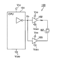
上述したブザー駆動回路として、例えば、図9に示されたものが提案されている。同図に示すように、ブザー駆動回路100は、ブザーBZと、ブザーBZを駆動するためのパルス状の駆動電圧VDを出力するCPU101と、駆動信号VDが入力されるバッファ102及びインバータ103と、を備えている。そして、上記ブザーBZは、これらバッファ102及びインバータ103の出力間に接続されている。
For example, the buzzer driving circuit shown in FIG. 9 has been proposed. As shown in the figure, the
上記ブザーBZは、その両端に印加されるパルス状のブザー電圧の振幅に応じた音圧のブザー音を出力する。上記CPU101は、5Vの電源電圧VCCの供給を受けて動作するものであり、この5V以下のパルス状の駆動電圧VDを出力する。上記バッファ102及びインバータ103は、CPU101と同様に5Vの電源電圧VDDの供給を受けて動作する。
The buzzer BZ outputs a buzzer sound having a sound pressure corresponding to the amplitude of the pulsed buzzer voltage applied to both ends thereof. The
以上の構成によれば、CPU101から出力される駆動電圧VDがHレベル(5V)のとき、バッファ102からは電源電圧VDDが出力されると共にインバータ103からはグランド電圧VGNDが出力される。これにより、ブザーBZのバッファ102側が電源電圧VDD、インバータ103側がグランド電圧VGNDとなる。
According to the above configuration, when the drive voltage V D output from the
一方、CPU101から出力される駆動電圧VDがLレベル(0V)のとき、バッファ102からはグランド電圧VGNDが出力されると共にインバータ103からは電源電圧VDDが出力される。これにより、ブザーBZのバッファ102側がグランド電圧VGND、インバータ103側が電源電圧VDDとなる。従って、ブザーBZの両端に印加されるブザー電圧の振幅は、バッファ102及びインバータ103の電源電圧VDD=5Vの2倍の10Vとなる。
On the other hand, when the drive voltage V D output from the
しかしながら、ブザー電圧の振幅が10Vだけでは、十分な音圧が確保できない。そこで、バッファ102及びインバータ103の電源電圧VDDを2倍の10Vにすることにより、ブザー電圧の振幅も2倍の20Vとして、十分な音圧が得られるようにすることが考えられる。
However, if the amplitude of the buzzer voltage is only 10V, sufficient sound pressure cannot be secured. Therefore, it is conceivable that the power voltage V DD of the
しかしながら、バッファ102及びインバータ103は、1/2VDD(VDD=10Vの場合は5V)以上の電圧が入力されないと、その出力をグランド電圧VGNDから電源電圧VDD、電源電圧VDDからグランド電圧VGNDに切り替えることができない。上述したようにCPU101から出力される駆動電圧VDは最大で5Vであり、1/2VDD以上の電圧とすることが難しい。このため、単にバッファ102及びインバータ103の電源電圧VDDを倍の10Vにしただけではバッファ102及びインバータ103の出力を切り替えることができず音を出すことができない。
However, if the voltage of 1/2 V DD (5 V when V DD = 10 V) or more is not inputted, the output of the
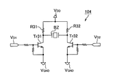
この問題を解決するために例えば図10に示されたブザー駆動回路104が考えられる。同図に示すように、ブザー駆動回路104は、ブザーBZと、10Vの電源電圧VDD間に互いに直列接続された抵抗R31及びトランジスタTr31と、電源電圧VDD間に互いに直列接続された抵抗R32及びトランジスタTr32と、を備えている。上記抵抗R31及びトランジスタTr31と、抵抗R32及びトランジスタTr32と、は互いに並列接続されている。そして、ブザーBZは、抵抗R31及びトランジスタTr31の接続点と、抵抗R32及びトランジスタTr32の接続点と、の間に接続されている。
In order to solve this problem, for example, the
また、トランジスタTr31のベースには、図示しないCPUからの5Vのパルス状の駆動電圧VD1が供給され、トランジスタTr32のベースには、図示しないCPUからの5Vのパルス状の駆動電圧VD2が供給されている。これら駆動電圧VD1及びVD2は、互いにHレベル、Lレベルが反転したパルス状の駆動電圧である。 Further, a 5 V pulsed drive voltage V D1 from a CPU (not shown) is supplied to the base of the transistor Tr31, and a 5 V pulsed drive voltage V D2 from a CPU (not shown) is supplied to the base of the transistor Tr32. Has been. These drive voltages V D1 and V D2 are pulsed drive voltages in which the H level and the L level are inverted from each other.
以上の構成によれば、図示しないCPUから出力される駆動電圧VD1がHレベル(5V)、駆動電圧VD2がLレベル(0V)のとき、トランジスタTr31がオン、トランジスタTr32がオフとなる。これにより、ブザーBZの抵抗R32側が、この抵抗R32を介して電源電圧VDDに接続され、ブザーBZの抵抗R31側がグランドに接続される。 According to the above configuration, when the drive voltage V D1 output from the CPU (not shown) is at the H level (5 V) and the drive voltage V D2 is at the L level (0 V), the transistor Tr31 is turned on and the transistor Tr32 is turned off. Thereby, the resistor R32 side of the buzzer BZ is connected to the power supply voltage V DD via the resistor R32, and the resistor R31 side of the buzzer BZ is connected to the ground.
一方、図示しないCPUから出力される駆動電圧VD1がLレベル(0V)、駆動電圧VD2がHレベル(5V)のとき、トランジスタTr31がオフ、トランジスタTr32がオンとなる。これにより、ブザーBZの抵抗R31側が、この抵抗R31を介して電源電圧VDDに接続され、抵抗R32側がグランドに接続される。従って、5Vの駆動電圧VD1、VD2でブザーBZの両端に10Vの電源電圧VDDを印加することができる。
On the other hand, when the drive voltage V D1 output from the CPU (not shown) is L level (0 V) and the drive voltage V D2 is H level (5 V), the transistor Tr31 is turned off and the transistor Tr32 is turned on. Thereby, the resistor R31 side of the buzzer BZ is connected to the power supply voltage V DD via the resistor R31, and the resistor R32 side is connected to the ground. Therefore, the power
しかしながら、上述したブザー駆動回路104によれば、例えばトランジスタTr31がオン、トランジスタTr32がオフしたときは、ブザーBZ及び抵抗R32が直列接続され、この直列接続されたブザーBZ及び抵抗R32に抵抗R31が並列接続されるため、抵抗R32を介してブザーBZに流れる電流に加えて、抵抗R31にも電流が流れるため、回路電流が増えてしまう。一方、トランジスタTr31がオフ、トランジスタTr32がオンしたときは、ブザーBZ及び抵抗R31が直列接続され、この直列接続されたブザーBZ及び抵抗R31に抵抗R32が並列接続されるため、抵抗R31を介してブザーBZに流れる電流に加えて、抵抗R32にも電流が流れるため、回路電流が増えてしまう。
However, according to the
結果、電源電圧VDDを発生する電源(ACトランス)が大きくなり、ブザー駆動回路104を小型化できない、という問題があった。このため、上記電源をスイッチング電源にすれば、ブザー駆動回路104での電流増加はトランスの大型に直結しないが電源回路のコストが上がってしまう。
As a result, there is a problem that the power supply (AC transformer) that generates the power supply voltage V DD becomes large and the
そこで、本発明は、ブザーの両端に印加されるブザー電圧を高くしてブザーの音圧を高くしつつ回路電流の低減を図ることにより、小型化できるブザー駆動回路を提供することを課題とする。 Accordingly, an object of the present invention is to provide a buzzer drive circuit that can be reduced in size by increasing the buzzer voltage applied to both ends of the buzzer and reducing the circuit current while increasing the sound pressure of the buzzer. .
上述した課題を解決するための請求項1記載の発明は、パルス状の駆動電圧を出力する出力手段と、前記駆動電圧の出力に応じて鳴動するブザーと、前記駆動電圧よりも高い電源電圧を供給する電圧源と、互いに極性が異なりかつ前記電源電圧間に直列接続された一対の第1トランジスタと、互いに極性が異なりかつ前記電源電圧間に直列接続されると共に前記一対の第1トランジスタに並列接続された一対の第2トランジスタと、を備え、前記ブザーが、前記一対の第1トランジスタ同士の接続点と前記一対の第2トランジスタ同士の接続点との間に接続され、前記一対の第1トランジスタの前記電源電圧プラス側及び前記一対の第2トランジスタの前記電源電圧マイナス側と、前記一対の第1トランジスタの前記電源電圧マイナス側及び前記一対の第2トランジスタの前記電源電圧プラス側と、のオンオフが互いに反転するように、前記一対の第1トランジスタ及び前記一対の第2トランジスタのベースに前記パルス状の駆動電圧が供給されたブザー駆動回路であって、前記出力手段からの駆動電圧を前記電源電圧系の電圧にシフトアップして前記一対の第1トランジスタのうち少なくとも前記電源電圧プラス側のベースに出力する第1レベルシフト回路と、前記出力手段からの駆動電圧を前記電源電圧系の電圧にシフトアップして前記一対の第2トランジスタのうち少なくとも前記電源電圧プラス側のベースに出力する第2レベルシフト回路と、をさらに備えたことを特徴とするブザー駆動回路に存する。 The invention described in claim 1 for solving the above-described problem is characterized in that an output means for outputting a pulsed drive voltage, a buzzer that rings in response to the output of the drive voltage, and a power supply voltage higher than the drive voltage. A voltage source to be supplied, a pair of first transistors having different polarities and connected in series between the power supply voltages, and a pair of first transistors having different polarities and connected in series between the power supply voltages and parallel to the pair of first transistors A pair of connected second transistors, wherein the buzzer is connected between a connection point between the pair of first transistors and a connection point between the pair of second transistors, and the pair of first transistors. The power supply voltage plus side of the transistor, the power supply voltage minus side of the pair of second transistors, the power supply voltage minus side of the pair of first transistors, and A buzzer in which the pulsed drive voltage is supplied to the bases of the pair of first transistors and the pair of second transistors so that the on / off state of the pair of second transistors with the power supply voltage plus side is reversed. A first level shift circuit for driving up the drive voltage from the output means to a voltage of the power supply voltage system and outputting it to at least the base on the power supply voltage plus side of the pair of first transistors; A second level shift circuit that shifts up the drive voltage from the output means to a voltage of the power supply voltage system and outputs it to at least the base on the power supply voltage plus side of the pair of second transistors. The present invention resides in a buzzer driving circuit.
請求項2記載の発明は、前記一対の第1トランジスタのうち前記電源電圧プラス側が、PNP型トランジスタで構成され、前記一対の第1トランジスタのうち前記電源電圧マイナス側が、NPN型トランジスタで構成され、前記一対の第2トランジスタのうち前記電源電圧プラス側が、PNP型トランジスタで構成され、前記一対の第2トランジスタのうち前記電源電圧マイナス側が、NPN型トランジスタで構成されていることを特徴とする請求項1記載のブザー駆動回路に存する。 According to the second aspect of the present invention, the power supply voltage plus side of the pair of first transistors is configured by a PNP transistor, and the power supply voltage minus side of the pair of first transistors is configured by an NPN transistor. The power supply voltage plus side of the pair of second transistors is configured by a PNP transistor, and the power supply voltage minus side of the pair of second transistors is configured by an NPN transistor. 1 is a buzzer driving circuit.
請求項3記載の発明は、前記出力手段が、互いにHレベル、Lレベルが反転した一対の前記パルス状の駆動電圧を出力し、前記第1レベルシフト回路が、前記一対の駆動電圧の一方をシフトアップすると共に当該一方の駆動電圧のHレベル、Lレベルを反転させて前記一対の第1トランジスタのうち前記電源電圧プラス側のベースのみに出力し、前記第2レベルシフト回路が、前記一対の駆動電圧の他方をシフトアップすると共に当該他方の駆動電圧のHレベル、Lレベルを反転させて前記一対の第2トランジスタのうち前記電源電圧プラス側のベースのみに出力し、前記一対の第1トランジスタのうち前記電源電圧マイナス側のベースには、前記一対の駆動電圧の他方が供給され、前記一対の第2トランジスタのうち前記電源電圧のマイナス側のベースには、前記一対の駆動電圧の一方が供給されていることを特徴とする請求項2に記載のブザー駆動回路に存する。 According to a third aspect of the present invention, the output means outputs a pair of pulsed drive voltages whose H level and L level are inverted with each other, and the first level shift circuit outputs one of the pair of drive voltages. Shifting up and inverting the H level and L level of the one drive voltage to output only to the base on the positive side of the power supply voltage of the pair of first transistors, and the second level shift circuit Shifting up the other of the drive voltages and inverting the H level and L level of the other drive voltage to output only to the base on the power supply voltage plus side of the pair of second transistors, and the pair of first transistors The other of the pair of drive voltages is supplied to the base on the negative side of the power supply voltage, and the minor of the power supply voltage of the pair of second transistors is supplied. The side of the base lies in the buzzer driving circuit according to claim 2, one of the pair of drive voltages is characterized in that it is supplied.
請求項4記載の発明は、前記一対の第1トランジスタ間に設けられた第1抵抗と、前記一対の第2トランジスタ間に設けられた第2抵抗と、をさらに備えたことを特徴とする請求項2又は3に記載のブザー駆動回路に存する。 The invention described in claim 4 further includes a first resistor provided between the pair of first transistors and a second resistor provided between the pair of second transistors. Item 4 or 3 is a buzzer driving circuit.
以上説明したように請求項1記載の発明によれば、駆動電圧よりも高い電源電圧間に一対の第1トランジスタ及び一対の第2トランジスタを設け、第1トランジスタ同士の接続点と第2トランジスタ同士の接続点との間にブザーを接続することにより、電源電圧の2倍に近い振幅をブザーの両端に印加することができ、ブザーの音圧を高くすることができる。また、このとき従来のようにブザーの両端に抵抗R31及びR32を設ける必要がなくなり回路電流を少なくして、電圧源の小型化を図ることができる。さらに、一対の第1トランジスタ及び一対の第2トランジスタのうち電源電圧プラス側は、この電源電圧の1/2よりも小さい出力手段からの駆動電圧がベースに供給されてもオンオフすることができないが、第1レベルシフト回路及び第2レベルシフト回路により駆動電圧をシフトアップすることにより、これら第1トランジスタ及び第2トランジスタに1/2電源電圧よりも大きい電圧をベースに供給することができ、第1トランジスタ及び第2トランジスタのオンオフが制御できるようになる。 As described above, according to the first aspect of the present invention, the pair of first transistors and the pair of second transistors are provided between the power supply voltages higher than the drive voltage, and the connection point between the first transistors and the second transistors are connected to each other. By connecting the buzzer between the two, the amplitude close to twice the power supply voltage can be applied to both ends of the buzzer, and the sound pressure of the buzzer can be increased. At this time, it is not necessary to provide the resistors R31 and R32 at both ends of the buzzer as in the prior art, and the circuit current can be reduced to reduce the size of the voltage source. Furthermore, the power supply voltage plus side of the pair of first transistors and the pair of second transistors cannot be turned on / off even when the drive voltage from the output means smaller than ½ of the power supply voltage is supplied to the base. By shifting up the drive voltage by the first level shift circuit and the second level shift circuit, it is possible to supply the first transistor and the second transistor with a voltage higher than the ½ power supply voltage as a base, The on / off state of the first transistor and the second transistor can be controlled.
請求項2記載の発明によれば、ブザーに印加されるブザー電圧の振幅を大きくすることができる。 According to invention of Claim 2, the amplitude of the buzzer voltage applied to a buzzer can be enlarged.
請求項3記載の発明によれば、一対の第1トランジスタのベース同士、一対の第2トランジスタのベース同士を共通接続しなくてもよいので、共通接続されたベースを通じて電流が流れることがなく、回路電流をさらに抑えることができる。 According to the invention of claim 3, since it is not necessary to connect the bases of the pair of first transistors and the bases of the pair of second transistors, current does not flow through the commonly connected bases. The circuit current can be further suppressed.
請求項4記載の発明によれば、一対の第1トランジスタ同士が同時にオンしても第1抵抗により一対の第1トランジスタに流れる電流を抑えることができる。また、一対の第2トランジスタ同士が同時にオンしても第2抵抗により一対の第2トランジスタに流れる電流を抑えることができる。 According to the fourth aspect of the present invention, even if the pair of first transistors are turned on at the same time, the current flowing through the pair of first transistors can be suppressed by the first resistor. Further, even when the pair of second transistors are turned on at the same time, the current flowing through the pair of second transistors can be suppressed by the second resistor.
第1実施形態
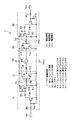
以下、第1実施形態における本発明のブザー駆動回路を図1及び図2に基づいて説明する。図1は、第1実施形態における本発明のブザー駆動回路を示す回路図である。図2(A)〜(H)は、図1に示すブザー駆動回路を構成するCPUから出力される駆動電圧VD1及びVD2、トランジスタTr5〜Tr8のオンオフ状態、駆動電圧Vb1及びVb2、トランジスタTr1〜Tr4のオンオフ状態を示すタイムチャートである。
First Embodiment Hereinafter, a buzzer driving circuit of the present invention in the first embodiment will be described with reference to FIGS. FIG. 1 is a circuit diagram showing a buzzer driving circuit of the present invention in the first embodiment. 2A to 2H show drive voltages V D1 and V D2 output from the CPU constituting the buzzer drive circuit shown in FIG. 1, the on / off states of the transistors Tr5 to Tr8, the drive voltages V b1 and V b2 , It is a time chart which shows the on-off state of transistor Tr1-Tr4.
上記ブザー駆動回路1は、パルス状の駆動電圧VD1、VD2を出力する図示しない出力手段としてのCPUと、この駆動電圧VD1、VD2の出力に応じて鳴動するブザーBZと、上記駆動電圧VD1、VD2の2倍以上の電源電圧VDDを供給する図示しない電圧源と、この電源電圧VDD間に互いに並列接続された第1プッシュプル回路21及び第2プッシュプル回路22と、第1レベルシフト回路31及び第2レベルシフト回路32と、抵抗Rと、を備えている。
The buzzer driving circuit 1 includes a CPU as output means (not shown) that outputs pulsed driving voltages V D1 and V D2 , a buzzer BZ that rings according to the outputs of the driving voltages V D1 and V D2 , and the driving A voltage source (not shown) that supplies a power supply voltage V DD that is twice or more the voltages V D1 and V D2 , and a first push-
上記図示しないCPUは、5Vの電源電圧の供給を受けて動作するものであり、約5Vのパルス状の駆動電圧VD1、VD2を出力する。上記駆動電圧VD1、VD2は、図2(A)及び(B)に示すように、互いにHレベル、Lレベルが反転している。上記ブザーBZは、その両端に印加されたパルス状のブザー電圧の振幅に応じた音圧のブザー音を出力する。上記図示しない電圧源は、5Vの駆動電圧VD1、VD2の2倍である10Vの電源電圧VDDを出力する。
The CPU (not shown) operates by receiving a power supply voltage of 5 V, and outputs about 5 V pulsed drive voltages V D1 and V D2 . As shown in FIGS. 2A and 2B, the driving voltages V D1 and V D2 are inverted in H level and L level. The buzzer BZ outputs a buzzer sound having a sound pressure corresponding to the amplitude of the pulsed buzzer voltage applied to both ends thereof. The voltage source (not shown) outputs a power
上記第1プッシュプル回路21は、互いに極性が異なりかつ電源電圧VDD間に直列接続された一対のNPN型のトランジスタTr1及びPNP型のトランジスタTr2(第1トランジスタ)から構成されている。これらトランジスタTr1及びトランジスタTr2は、その接続点を中心に対称配置されている。
The first push-
即ち、トランジスタTr1及びトランジスタTr2のエミッタ同士が接続され、トランジスタTr1のコレクタが電源電圧VDDに接続され、トランジスタTr2のコレクタがグランド電圧VGNDに接続されている。また、これらトランジスタTr1及びTr2のベースは互いに共通接続されて、後述する第1レベルシフト回路31から出力される駆動電圧Vb1が供給されている。
That is, the emitters of the transistor Tr1 and the transistor Tr2 are connected to each other, the collector of the transistor Tr1 is connected to the power supply voltage VDD, and the collector of the transistor Tr2 is connected to the ground voltage VGND . The bases of the transistors Tr1 and Tr2 are commonly connected to each other and supplied with a drive voltage V b1 output from a first
上記第2プッシュプル回路22は、互いに極性が異なりかつ電源電圧VDD間に直列接続された一対のNPN型のトランジスタTr3及びPNP型のトランジスタTr4(第2トランジスタ)から構成されている。これらトランジスタTr3及びトランジスタTr4は、その接続点を中心に対称配置されている。
The second push-
即ち、トランジスタTr3及びトランジスタTr4のエミッタ同士が接続され、トランジスタTr3のコレクタが電源電圧VDDに接続され、トランジスタTr4のコレクタがグランド電圧VGNDに接続されている。また、これらトランジスタTr3及びTr4のベースは互いに共通接続されて、後述する第2レベルシフト回路32から出力される駆動電圧Vb2が供給されている。上記ブザーBZは、トランジスタTr1及びTr2の接続点と、トランジスタTr3及びTr4の接続点と、の間に接続されている。
That is, emitters of the transistors Tr3 and the transistor Tr4 is connected, the collector of the transistor Tr3 is connected to the power supply voltage V DD, the collector of the transistor Tr4 is connected to the ground voltage V GND. The bases of the transistors Tr3 and Tr4 are commonly connected to each other, and supplied with a drive voltage V b2 output from a second
上記第1レベルシフト回路31は、5Vの駆動電圧VD1を電源電圧VDD系のHレベルがほぼ10V、Lレベルが0Vの駆動電圧Vb1にシフトアップして一対のトランジスタTr1及びTr2のベースに供給する回路である。上記第1レベルシフト回路31は、トランジスタTr5及びTr6と、抵抗R1〜R5と、を備えている。
The first
上記トランジスタTr5は、そのエミッタが電源電圧VDDに接続され、コレクタが抵抗R1を介してグランド電圧VGNDに接続されている。そして、このトランジスタTr5のコレクタと抵抗R1との接続点が、抵抗R6を介してトランジスタTr1及びTr2のベースに接続されている。また、トランジスタTr5のベース−エミッタ間には上記抵抗R2が接続されている。 The transistor Tr5 has an emitter connected to the power supply voltage V DD and a collector connected to the ground voltage V GND via the resistor R1. The connection point between the collector of the transistor Tr5 and the resistor R1 is connected to the bases of the transistors Tr1 and Tr2 via the resistor R6. The resistor R2 is connected between the base and emitter of the transistor Tr5.
上記トランジスタTr6は、そのエミッタがグランド電圧VGNDに接続され、コレクタが抵抗R3を介してトランジスタTr5のベースに接続されている。また、トランジスタTr6のベース−エミッタ間に抵抗R4が接続されていて、トランジスタTr6のベースには抵抗R5を介して駆動電圧VD1が出力される。 The emitter of the transistor Tr6 is connected to the ground voltage VGND , and the collector is connected to the base of the transistor Tr5 via the resistor R3. A resistor R4 is connected between the base and emitter of the transistor Tr6, and the drive voltage V D1 is output to the base of the transistor Tr6 via the resistor R5.
以上の構成によれば、図2(A)及び(C)に示すように、駆動電圧VD1がH(5V)のときはトランジスタTr6のエミッタ−ベース間にバイアス電圧が印加されトランジスタTr6がオンする。このトランジスタTr6のオンにより抵抗R2及びR3の両端に電源電圧VDDが供給されるため、抵抗R2に発生する電圧降下分、トランジスタTr5のベースがエミッタよりも低くなりエミッタ−ベース間にバイアス電圧が印加されトランジスタTr5がオンする。このトランジスタTr5のオンによりほぼ電源電圧VDDに等しい10Vの駆動電圧Vb1がトランジスタTr1及びTr2のベースに出力される。 According to the above configuration, as shown in FIGS. 2A and 2C, when the drive voltage V D1 is H (5 V), a bias voltage is applied between the emitter and base of the transistor Tr6, and the transistor Tr6 is turned on. To do. Since the power supply voltage V DD is supplied to both ends of the resistors R2 and R3 by turning on the transistor Tr6, the base of the transistor Tr5 becomes lower than the emitter by the voltage drop generated in the resistor R2, and a bias voltage is generated between the emitter and the base. Applied, transistor Tr5 is turned on. The 10V drive voltage V b1 is equal to approximately the power supply voltage V DD by turning on the transistor Tr5 is output to the base of the transistor Tr1 and Tr2.
一方、駆動電圧VD1がL(0V)のときはトランジスタTr6のエミッタ−ベース間電圧が0となりトランジスタTr6がオフする。このトランジスタTr6のオフにより抵抗R2及びR3の両端に供給された電源電圧VDDが遮断されるため、トランジスタTr5のエミッタ−ベース電圧が0となりトランジスタTr5がオフする。 On the other hand, when the drive voltage V D1 is L (0 V), the emitter-base voltage of the transistor Tr6 becomes 0 and the transistor Tr6 is turned off. Since the transistor Tr6 is turned off, the power supply voltage V DD supplied to both ends of the resistors R2 and R3 is cut off, so that the emitter-base voltage of the transistor Tr5 becomes 0 and the transistor Tr5 is turned off.
このトランジスタTr5のオフによりグランド電圧VGNDに等しい0Vの駆動電圧Vb1がトランジスタTr1及びTr2のベースに出力される。よって、図2(A)及び(E)に示すように、トランジスタTr1及びTr2のベースには、駆動電圧VD1と同位相であり、振幅が10Vのパルス状の駆動電圧Vb1が供給される。 The driving voltage V b1 off by the 0V equal to ground voltage V GND of the transistor Tr5 is output to the base of the transistor Tr1 and Tr2. Therefore, as shown in FIGS. 2A and 2E, the bases of the transistors Tr1 and Tr2 are supplied with a pulsed drive voltage V b1 having the same phase as the drive voltage V D1 and an amplitude of 10 V. .
上記第2レベルシフト回路32は、5Vの駆動電圧VD2を電源電圧VDD系のほぼ10Vの駆動電圧Vb2にシフトアップして一対のトランジスタTr3及びTr4のベースに供給する回路である。上記第2レベルシフト回路32は、トランジスタTr7及びTr8と、抵抗R7〜R11と、を備えている。
The second
上記トランジスタTr7は、そのエミッタが電源電圧VDDに接続され、コレクタが抵抗R7を介してグランド電圧VGNDに接続されている。そして、このトランジスタTr7のコレクタと抵抗R7との接続点が、抵抗R12を介してトランジスタTr3及びTr4のベースに接続されている。また、トランジスタTr7のベース−エミッタ間には上記抵抗R8が接続されている。 The transistor Tr7 has its emitter connected to the power supply voltage V DD, is connected to the ground voltage V GND collector through a resistor R7. The connection point between the collector of the transistor Tr7 and the resistor R7 is connected to the bases of the transistors Tr3 and Tr4 via the resistor R12. The resistor R8 is connected between the base and emitter of the transistor Tr7.
上記トランジスタTr8は、そのエミッタがグランド電圧VGNDに接続され、コレクタが抵抗R9を介してトランジスタTr7のベースに接続されている。また、トランジスタTr8のベース−エミッタ間に抵抗R10が接続されていて、トランジスタTr8のベースには抵抗R11を介して駆動電圧VD2が出力される。 The transistor Tr8 has its emitter connected to the ground voltage V GND, and is connected collector through a resistor R9 to the base of the transistor Tr7. A resistor R10 is connected between the base and emitter of the transistor Tr8, and the drive voltage V D2 is output to the base of the transistor Tr8 via the resistor R11.
以上の構成によれば、図2(B)及び(D)に示すように、駆動電圧VD2がH(5V)のときはトランジスタTr8のエミッタ−ベース間にバイアス電圧が印加されトランジスタTr8がオンする。このトランジスタTr8のオンにより抵抗R8及びR9の両端に電源電圧VDDが供給されるため、抵抗R8に発生する電圧降下分、トランジスタTr7のベースがエミッタよりも低くなりエミッタ−ベース間にバイアス電圧が印加されトランジスタTr7がオンする。このトランジスタTr7のオンによりほぼ電源電圧VDDに等しい10Vの駆動電圧Vb2がトランジスタTr3及びTr4のベースに出力される。 According to the above configuration, as shown in FIGS. 2B and 2D, when the drive voltage V D2 is H (5 V), a bias voltage is applied between the emitter and base of the transistor Tr8 and the transistor Tr8 is turned on. To do. Since the power supply voltage V DD is supplied to both ends of the resistors R8 and R9 by turning on the transistor Tr8, the base of the transistor Tr7 is lower than the emitter by the voltage drop generated in the resistor R8, and the bias voltage is set between the emitter and the base. Applied, transistor Tr7 is turned on. The 10V drive voltage V b2 is equal to approximately the power supply voltage V DD by turning on the transistor Tr7 is output to the base of the transistor Tr3 and Tr4.
一方、駆動電圧VD2がL(0V)のときはトランジスタTr8のエミッタ−ベース間電圧が0となりトランジスタTr8がオフする。このトランジスタTr8のオフにより抵抗R8及びR9の両端に供給された電源電圧VDDが遮断されるため、トランジスタTr7のエミッタ−ベース電圧が0となりトランジスタTr7がオフする。 On the other hand, when the drive voltage V D2 is L (0 V), the emitter-base voltage of the transistor Tr8 becomes 0 and the transistor Tr8 is turned off. Since the power supply voltage V DD supplied to both ends of the resistors R8 and R9 is cut off by turning off the transistor Tr8, the emitter-base voltage of the transistor Tr7 becomes 0 and the transistor Tr7 is turned off.
このトランジスタTr7のオフによりほぼグランド電圧VGNDに等しい0Vの駆動電圧Vb2がトランジスタTr3及びTr4のベースに出力される。よって、図2(B)及び(F)に示すように、トランジスタTr3及びTr4のベースには、駆動電圧VD2と同位相であり、振幅が10Vのパルス状の駆動電圧Vb2が供給される。また、上記抵抗Rは、音色の歪みをなくすために、トランジスタTr1及びTr2の接続点とブザーBZとの間に接続されている。 The driving voltage V b2 of 0V approximately equal to the ground voltage V GND by turning off the transistor Tr7 is output to the base of the transistor Tr3 and Tr4. Therefore, as shown in FIGS. 2B and 2F, the bases of the transistors Tr3 and Tr4 are supplied with a pulsed drive voltage V b2 having the same phase as the drive voltage V D2 and an amplitude of 10V. . The resistor R is connected between the connection point of the transistors Tr1 and Tr2 and the buzzer BZ in order to eliminate distortion of the timbre.
次に、上述した構成のブザー駆動回路1の動作について、図2のタイムチャートを参照して説明する。CPUから互いにHレベル、Lレベルが反転した駆動電圧VD1、VD2が出力されると、図2(E)に示すように、第1レベルシフト回路31が、5Vの駆動電圧VD1を10Vの駆動電圧Vb1にレベルアップして、トランジスタTr1及びTr2のベースに供給する。また、図2(F)に示すように、第2レベルシフト回路32が、5Vの駆動電圧VD2を10Vの駆動電圧Vb2にレベルアップして、トランジスタTr3及びTr4のベースに供給する。
Next, the operation of the buzzer driving circuit 1 configured as described above will be described with reference to the time chart of FIG. When the drive voltages V D1 and V D2 in which the H level and the L level are inverted from each other are output from the CPU, the first
図2(G)及び(H)に示すように、駆動電圧Vb1がL(0V)、駆動電圧Vb2がH(10V)のときは、トランジスタTr1及びTr4がオフして、トランジスタTr2及びTr3がオンして、ブザーBZの第1プッシュプル回路21側にグランド電圧VGNDが接続され、第2プッシュプル回路22側に電源電圧VDDが接続される。これに対して、駆動電圧Vb1、Vb2が反転して、駆動電圧Vb1がH(10V)、駆動電圧Vb2がL(0V)のときは、トランジスタTr1及びTr4がオンして、トランジスタTr2及びTr3がオフして、ブザーBZの第2プッシュプル回路21側に電源電圧VDDが接続され、第1プッシュプル回路21側にグランド電圧VGNDが接続される。即ち、トランジスタTr1及びTr4のオンオフとトランジスタTr2及びTr3のオンオフとが互いに反転され、ブザーBZの一端及び他端が交互に電源電圧VDDに接続されることにより、ブザーBZに印加されるブザー電圧VBZの振幅はほぼ電源電圧VDDの2倍弱となる。
As shown in FIGS. 2G and 2H , when the drive voltage V b1 is L (0 V) and the drive voltage V b2 is H (10 V), the transistors Tr1 and Tr4 are turned off and the transistors Tr2 and Tr3 are turned off. Is turned on, the ground voltage V GND is connected to the first push-
次に、図3を参照してブザー電圧VBZについて説明する。今、図3に示すように、トランジスタTr1及びTr4がオン、トランジスタTr2及びTr3がオフして、ブザーBZの第1プッシュプル回路21側に電源電圧VDDが接続され、第2プッシュプル回路22側にグランド電圧VGNDが接続された場合について考えて見る。NPN型のトランジスタTr1のベースコレクタ間は、ベースからコレクタに向かう方向が順方向となるダイオードD1に等価でき、ベースエミッタ間は、ベースからエミッタに向かう方向が順方向となるダイオードD2に等価できる。一方、PNP型のトランジスタTr4のエミッタコレクタ間は、エミッタからベースに向かう方向が順方向となるダイオードD3に等価でき、ベースコレクタ間は、コレクタからベースに向かう方向が順方向となるダイオードD4に等価できる。
Next, the buzzer voltage V BZ will be described with reference to FIG. Now, as shown in FIG. 3, the transistors Tr1 and Tr4 are turned on, the transistors Tr2 and Tr3 are turned off, and the power supply voltage V DD is connected to the first push-
よって、ブザーBZの一端にはトランジスタTr1のベースエミッタ間を介して10Vが供給され、他端にはトランジスタTr4のベースエミッタ間を介して0Vが供給されているため、ブザー電圧VBZは下記の式(1)で表す値となる。
VBZ=10V(VDD)−0.8V(トランジスタTr1のベースエミッタ間電圧)−0.8(トランジスタTr4のベースエミッタ間電圧)=8.4V…(1)
結果、ブザー電圧VBZの振幅はその2倍の16.8Vとなる。
Therefore, 10V is supplied to one end of the buzzer BZ via the base emitter of the transistor Tr1, and 0V is supplied to the other end of the buzzer BZ via the base emitter of the transistor Tr4. It becomes a value represented by Formula (1).
V BZ = 10 V (V DD ) −0.8 V (base-emitter voltage of transistor Tr1) −0.8 (base-emitter voltage of transistor Tr4) = 8.4 V (1)
As a result, the amplitude of the buzzer voltage V BZ is 16.8V, which is twice that.
上述したブザー駆動回路1によれば、駆動電圧VD1、VD2よりも高い電源電圧VDD間に一対のトランジスタTr1、Tr2と、一対のトランジスタTr3、Tr4とを並列に設け、トランジスタTr1、Tr2同士の接続点とトランジスタTr3、Tr4の接続点との間にブザーBZを接続することにより、電源電圧VDDの2倍に近い振幅をブザーBZの両端に印加することができ、ブザーBZの音圧を高くすることができる。また、このとき従来のようにブザーBZの両端に抵抗R31及びR32を設ける必要がなくなり回路電流を少なくして、電圧源の小型化を図ることができる。さらに、トランジスタTr1、Tr2の接続点、トランジスタTr3、Tr4の接続点の電圧は、ほぼ1/2VDDとなる。従って、トランジスタTr1及びTr3は、この1/2VDDよりも低い5Vの駆動電圧VD1、VD2がベースに供給されてもオンオフすることができないが、第1レベルシフト回路21及び第2レベルシフト回路22を設けることにより、これらトランジスタTr1及びTr3に1/2VDDよりも大きい駆動電圧Vb1、Vb2をベースに供給することができ、トランジスタTr1及びTr3のオンオフが制御できるようになる。
According to the buzzer driving circuit 1 described above, a pair of transistors Tr1, Tr2 and a pair of transistors Tr3, Tr4 are provided in parallel between the power supply voltages V DD higher than the driving voltages V D1 , V D2 , and the transistors Tr1, Tr2 By connecting the buzzer BZ between the connection point between the transistors Tr3 and Tr4, an amplitude close to twice the power supply voltage V DD can be applied to both ends of the buzzer BZ. The pressure can be increased. At this time, it is not necessary to provide the resistors R31 and R32 at both ends of the buzzer BZ as in the prior art, so that the circuit current can be reduced and the voltage source can be downsized. Further, the voltage at the connection point between the transistors Tr1 and Tr2 and the connection point between the transistors Tr3 and Tr4 is approximately 1 / 2V DD . Therefore, the transistors Tr1 and Tr3 cannot be turned on / off even when the drive voltages V D1 and
第2実施形態
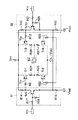
次に、第2実施形態における本発明のブザー駆動回路を図4に基づいて説明する。図4は、第2実施形態における本発明のブザー駆動回路を示す回路図である。第1実施形態と第2実施形態とで大きく異なる点は、トランジスタTr1〜Tr1の極性である。即ち、第1実施形態では、NPN型のトランジスタTr1及びTr3、PNP型のトランジスタTr2及びTr4を用いていたが、第2実施形態ではプッシュプル回路を廃止してPNP型のトランジスタTr1及びTr3、NPN型のトランジスタTr2及びTr4を用いている。なお、トランジスタTr1〜Tr4の極性を変えることにより、第2実施形態においては、駆動電圧VD1がHレベル、駆動電圧VD2がLレベルのときは、第1実施形態とは逆に、トランジスタTr1及びTr4がオフ、トランジスタTr2及びTr3がオンし、駆動電圧VD1がLレベル、駆動電圧VD2がHレベルのときは、トランジスタTr1及びTr4がオン、トランジスタTr2及びTr3がオフする。
Second Embodiment Next, a buzzer driving circuit of the present invention in a second embodiment will be described with reference to FIG. FIG. 4 is a circuit diagram showing a buzzer driving circuit of the present invention in the second embodiment. A major difference between the first embodiment and the second embodiment is the polarity of the transistors Tr1 to Tr1. That is, in the first embodiment, the NPN transistors Tr1 and Tr3 and the PNP transistors Tr2 and Tr4 are used. However, in the second embodiment, the push-pull circuit is eliminated and the PNP transistors Tr1 and Tr3, NPN are used. Type transistors Tr2 and Tr4 are used. Note that by changing the polarity of the transistors Tr1 to Tr4, in the second embodiment, when the drive voltage V D1 is at the H level and the drive voltage V D2 is at the L level, the transistor Tr1 is opposite to the first embodiment. And Tr4 are off, transistors Tr2 and Tr3 are on, drive voltage V D1 is L level, and drive voltage V D2 is H level, transistors Tr1 and Tr4 are on and transistors Tr2 and Tr3 are off.
これにより、ブザー電圧VBZの振幅を第1実施形態よりも大きくすることができる。この効果について説明する。今、図5に示すように、トランジスタTr1及びTr4がオン、トランジスタTr2及びTr3がオフして、ブザーBZのトランジスタTr1側に電源電圧VDDが接続され、トランジスタTr4側にグランド電圧VGNDが接続された場合について考えて見る。PNP型のトランジスタTr1のベースエミッタ間は、エミッタからベースに向かう方向が順方向となるダイオードD5に等価でき、ベースコレクタ間は、コレクタからベースに向かう方向が順方向となるダイオードD6に等価できる。一方、NPN型のトランジスタTr4のベースコレクタ間は、ベースからコレクタに向かう方向が順方向となるダイオードD7に等価でき、ベースエミッタ間は、ベースからエミッタに向かう方向が順方向となるダイオードD8に等価できる。 Thereby, the amplitude of the buzzer voltage V BZ can be made larger than that in the first embodiment. This effect will be described. As shown in FIG. 5, the transistors Tr1 and Tr4 are turned on, the transistors Tr2 and Tr3 are turned off, the power supply voltage V DD is connected to the transistor Tr1 side of the buzzer BZ, and the ground voltage V GND is connected to the transistor Tr4 side. See if you think about it. The distance between the base and emitter of the PNP transistor Tr1 can be equivalent to a diode D5 whose forward direction is from the emitter to the base, and the distance between the base and collector can be equivalent to a diode D6 whose forward direction is from the collector to the base. On the other hand, the distance between the base and collector of the NPN transistor Tr4 can be equivalent to a diode D7 whose forward direction is from the base to the collector, and the distance between the base and emitter is equivalent to a diode D8 whose forward direction is from the base to the emitter. it can.
よって、ブザーBZの一端にはトランジスタTr1のコレクタエミッタ間を介して10Vが供給され、他端にはトランジスタTr4のコレクタエミッタ間を介して0Vが供給されているため、ブザー電圧VBZは下記の式(2)で表す値となる。
VBZ=10V(VDD)−0.1V(トランジスタTr1のコレクタエミッタ間電圧Vce)−0.1(トランジスタTr4のコレクタエミッタ間電圧Vce)=9.8V…(2)
結果、ブザー電圧VBZの振幅はその2倍の19.6Vとなり、第1実施形態よりも振幅を大きくして音圧を高くできる。
Therefore, the one end of the buzzer BZ is supplied with 10V via the collector-emitter of the transistors Tr1, because it is supplied with 0V via the collector-emitter of the transistor Tr4 is on the other end, the buzzer voltage V BZ is below It becomes a value represented by Formula (2).
V BZ = 10 V (V DD ) −0.1 V (the collector-emitter voltage Vce of the transistor Tr1) −0.1 (the collector-emitter voltage Vce of the transistor Tr4) = 9.8 V (2)
As a result, the amplitude of the buzzer voltage V BZ is 19.6 V, twice that of the buzzer voltage V BZ , and the sound pressure can be increased by making the amplitude larger than in the first embodiment.
第3実施形態
次に、第3実施形態について説明する。ところで、上述した第2実施形態では、図6に示すように、トランジスタTr1及びT2のベース、トランジスタTr3及びTr4のベースを共通接続すると、トランジスタTr1、Tr3のベースエミッタ間に等価されるダイオードD5と、トランジスタTr2、Tr4のベースエミッタ間に等価されるダイオードD8と、の順方向が電源電圧VDDの印加方向と同一になってしまうため、図中点線で示すように、トランジスタTr1〜Tr4がオフのときに共通接続されたベースを介して電流が流れてしまう。
Third Embodiment Next, a third embodiment will be described. By the way, in the second embodiment described above, as shown in FIG. 6, when the bases of the transistors Tr1 and T2 and the bases of the transistors Tr3 and Tr4 are connected in common, the diode D5 equivalent between the base emitters of the transistors Tr1 and Tr3 Since the forward direction of the diode D8 equivalent between the base emitters of the transistors Tr2 and Tr4 becomes the same as the application direction of the power supply voltage V DD , the transistors Tr1 to Tr4 are turned off as indicated by the dotted line in the figure. In this case, current flows through the commonly connected bases.
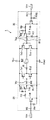
第3実施形態では、図7に示すように、第2実施形態と同様にPNP型のトランジスタTr1及びTr2、NPN型のトランジスタTr3及びTr4を用いて、トランジスタTr1及びTr2のベース同士、トランジスタTr3及びTr4のベース同士を共通接続しない構成にしている。即ち、トランジスタTr1のベースには後述する第1レベルシフト回路31から出力される駆動電圧Vb1が供給され、トランジスタTr2のベースには駆動電圧VD2が抵抗R21、R20、R22を介して供給されている。また、トランジスタTr3のベースには後述する第2レベルシフト回路32から出力される駆動電圧Vb2が供給され、トランジスタTr4のベースには駆動電圧VD1が抵抗R17、R16、R23を介して供給されている。
In the third embodiment, as shown in FIG. 7, using the PNP transistors Tr1 and Tr2 and the NPN transistors Tr3 and Tr4 as in the second embodiment, the bases of the transistors Tr1 and Tr2, the transistors Tr3 and The Tr4 bases are not connected in common. That is, the drive voltage V b1 output from the first
また、第2実施形態と第3実施形態とで大きく異なる点は、第1レベルシフト回路31と第2レベルシフト回路32との構成である。上記第1レベルシフト回路31は、Hレベルが5V、Lレベルが0Vの駆動電圧VD1をHレベルが10V(≒VDD)、Lレベルが電源電圧VDDを抵抗R14及びR15で分圧した分圧値(例えば5V)となる駆動電圧Vb1にシフトアップする。さらに、第1レベルシフト回路31は、駆動電圧VD1のHレベル、Lレベルを反転させてトランジスタTr1のベースに出力する。上記第1レベルシフト回路31は、NPN型のトランジスタTr9と、抵抗R14〜R17と、を備えている。
A significant difference between the second embodiment and the third embodiment is the configuration of the first
上記トランジスタTr9は、そのコレクタが抵抗R14を介して電源電圧VDDに接続され、エミッタが抵抗R15を介してグランド電圧VGNDに接続されている。そして、このトランジスタTr9のコレクタと抵抗R14との接続点が、抵抗R6を介してトランジスタTr1のベースに接続されている。また、トランジスタTr9のベース−エミッタ間には上記抵抗R16が接続され、トランジスタTr9のベースには抵抗R17を介して駆動電圧VD1が供給されている。 The transistor Tr9 has a collector connected to the power supply voltage V DD via the resistor R14, and an emitter connected to the ground voltage V GND via the resistor R15. A connection point between the collector of the transistor Tr9 and the resistor R14 is connected to the base of the transistor Tr1 through the resistor R6. The resistor R16 is connected between the base and emitter of the transistor Tr9, and the drive voltage V D1 is supplied to the base of the transistor Tr9 via the resistor R17.
以上の構成によれば、図8(A)及び(C)に示すように、駆動電圧VD1がH(5V)のときはトランジスタTr9のエミッタ−ベース間にバイアス電圧が印加されトランジスタTr9がオンする。このトランジスタTr9のオンにより電源電圧VDDを抵抗14及びR15で分圧した値(例えば5V)となる駆動電圧Vb1がトランジスタTr1のベースに出力される。 According to the above configuration, as shown in FIGS. 8A and 8C, when the drive voltage V D1 is H (5 V), a bias voltage is applied between the emitter and base of the transistor Tr9 and the transistor Tr9 is turned on. To do. This on the power supply voltage V DD resistors 14 and divided by the value in R15 of the transistor Tr9 (eg 5V) to become the driving voltage V b1 is outputted to the base of the transistor Tr1.
一方、駆動電圧VD1がL(0V)のときはトランジスタTr9のエミッタ−ベース間電圧が0となりトランジスタTr9がオフする。このトランジスタTr9のオフによりほぼ電源電圧VDDに等しい10Vの駆動電圧Vb1がトランジスタTr1のベースに出力される。よって、図8(A)及び(E)に示すように、トランジスタTr1のベースには、駆動電圧VD1のHレベル、Lレベルを反転させた即ち、駆動電圧VD2と同位相であり、Lレベルが5V、Hレベルが10Vのパルス状の駆動電圧Vb1が供給される。 On the other hand, when the drive voltage V D1 is L (0 V), the emitter-base voltage of the transistor Tr9 becomes 0 and the transistor Tr9 is turned off. The 10V drive voltage V b1 is equal to approximately the power supply voltage V DD by turning off the transistor Tr9 is output to the base of the transistor Tr1. Therefore, as shown in FIGS. 8A and 8E, the H level and L level of the drive voltage V D1 are inverted at the base of the transistor Tr1, that is, in phase with the drive voltage V D2 and L A pulsed drive voltage V b1 having a level of 5 V and an H level of 10 V is supplied.
上記第2レベルシフト回路32は、Hレベルが5V、Lレベルが0Vの駆動電圧VD2をHレベルが10V(≒VDD)、Lレベルが電源電圧VDDを抵抗R18及びR19で分圧した分圧値(例えば5V)となる駆動電圧Vb2にシフトアップする。さらに、第2レベルシフト回路32は、駆動電圧VD2のHレベル、Lレベルを反転させてトランジスタTr3のベースに出力する。上記第1レベルシフト回路32は、NPN型のトランジスタTr10と、抵抗R18〜R21と、を備えている。
The second
上記トランジスタTr10は、そのコレクタが抵抗R18を介して電源電圧VDDに接続され、エミッタが抵抗R19を介してグランド電圧VGNDに接続されている。そして、このトランジスタTr10のコレクタと抵抗R18との接続点が、抵抗R12を介してトランジスタTr3のベースに接続されている。また、トランジスタTr10のベース−エミッタ間には上記抵抗R20が接続され、トランジスタTr10のベースには抵抗R21を介して駆動電圧VD2が供給されている。 The transistor Tr10 has a collector connected to the power supply voltage V DD via the resistor R18, and an emitter connected to the ground voltage V GND via the resistor R19. The connection point between the collector of the transistor Tr10 and the resistor R18 is connected to the base of the transistor Tr3 via the resistor R12. The resistor R20 is connected between the base and emitter of the transistor Tr10, and the drive voltage V D2 is supplied to the base of the transistor Tr10 via the resistor R21.
以上の構成によれば、図8(B)及び(D)に示すように、駆動電圧VD2がH(5V)のときはトランジスタTr10のエミッタ−ベース間にバイアス電圧が印加されトランジスタTr10がオンする。このトランジスタTr10のオンにより電源電圧VDDを抵抗R18及びR19で分圧した値(例えば5V)となる駆動電圧Vb2がトランジスタTr3のベースに出力される。 According to the above configuration, as shown in FIGS. 8B and 8D, when the drive voltage V D2 is H (5 V), a bias voltage is applied between the emitter and base of the transistor Tr10 and the transistor Tr10 is turned on. To do. When the transistor Tr10 is turned on, a drive voltage V b2 having a value (for example, 5 V) obtained by dividing the power supply voltage V DD by the resistors R18 and R19 is output to the base of the transistor Tr3.
一方、駆動電圧VD2がL(0V)のときはトランジスタTr10のエミッタ−ベース間電圧が0となりトランジスタTr10がオフする。このトランジスタTr10のオフによりほぼ電源電圧VDDに等しい10Vの駆動電圧Vb2がトランジスタTr3のベースに出力される。よって、図8(B)及び(F)に示すように、トランジスタTr3のベースには、駆動電圧VD2のHレベル、Lレベルを反転させた即ち、駆動電圧VD1と同位相であり、Lレベルが5V、Hレベルが10Vのパルス状の駆動電圧Vb2が供給される。 On the other hand, when the drive voltage V D2 is L (0 V), the emitter-base voltage of the transistor Tr10 becomes 0 and the transistor Tr10 is turned off. The 10V drive voltage V b2 is equal to approximately the power supply voltage V DD by turning off the transistor Tr10 is output to the base of the transistor Tr3. Therefore, as shown in FIGS. 8B and 8F, the H level and L level of the drive voltage V D2 are inverted at the base of the transistor Tr3, that is, in phase with the drive voltage V D1 , L A pulsed drive voltage V b2 having a level of 5 V and an H level of 10 V is supplied.
また、上記トランジスタTr1及びTr2の間には第1抵抗としての抵抗R24及びR25が接続され、トランジスタTr3及びTr4の間には第2抵抗としての抵抗R26及びR27が接続されている。これら抵抗R24〜R27は、音色の歪みをなくすために設けられている。 Further, resistors R24 and R25 as first resistors are connected between the transistors Tr1 and Tr2, and resistors R26 and R27 as second resistors are connected between the transistors Tr3 and Tr4. These resistors R24 to R27 are provided to eliminate timbre distortion.
次に、上述した構成のブザー駆動回路1の動作について、図8のタイムチャートを参照して説明する。CPUから互いにH、Lが反転した駆動電圧VD1、VD2が出力されると、図8(E)に示すように、トランジスタTr1のベースには、第1レベルシフト回路31から出力される駆動電圧Vb1が供給される。また、図8(B)に示すように、トランジスタTr2のベースには、第2レベルシフト回路32から出力される駆動電圧Vb2が供給される。
Next, the operation of the buzzer driving circuit 1 configured as described above will be described with reference to the time chart of FIG. When the drive voltages V D1 and V D2 in which H and L are inverted from each other are output from the CPU, the drive output from the first
駆動電圧Vb1がLレベル(5V)、駆動電圧Vb2がHレベル(10V)のときは、トランジスタTr1及びTr4がオンして、トランジスタTr2及びTr3がオフして、ブザーBZのトランジスタTr1側に電源電圧VDDが接続され、トランジスタTr4側にグランド電圧VGNDが接続される。これに対して、駆動電圧Vb1、Vb2が反転して、駆動電圧Vb1がHレベル(10V)、駆動電圧Vb2がLレベル(5V)のときは、トランジスタTr2及びTr3がオンして、トランジスタTr1及びTr4がオフして、ブザーBZのトランジスタTr3側に電源電圧VDDが接続され、トランジスタTr2側にグランド電圧VGNDが接続される。このようにブザーBZの一端及び他端が交互に電源電圧VDDに接続されることにより、ブザーBZに印加される電圧の振幅はほぼ電源電圧VDDの2倍弱となる。 When the drive voltage V b1 is L level (5 V) and the drive voltage V b2 is H level (10 V), the transistors Tr1 and Tr4 are turned on, the transistors Tr2 and Tr3 are turned off, and the buzzer BZ is turned to the transistor Tr1 side. The power supply voltage V DD is connected, and the ground voltage V GND is connected to the transistor Tr4 side. On the other hand, when the drive voltages V b1 and V b2 are inverted, the drive voltage V b1 is H level (10 V), and the drive voltage V b2 is L level (5 V), the transistors Tr2 and Tr3 are turned on. The transistors Tr1 and Tr4 are turned off, the power supply voltage V DD is connected to the transistor Tr3 side of the buzzer BZ, and the ground voltage V GND is connected to the transistor Tr2 side. Thus, by alternately connecting one end and the other end of the buzzer BZ to the power supply voltage V DD , the amplitude of the voltage applied to the buzzer BZ is almost less than twice the power supply voltage V DD .
上述した第3実施形態のブザー駆動回路1によれば、一対のトランジスタTr1、Tr2のベース同士、一対のトランジスタTr3、Tr4のベース同士を共通接続しなくても良いので、共通接続されたベースを通じて電流が流れることなく、回路電流をさらに抑えることができる。 According to the buzzer driving circuit 1 of the third embodiment described above, the bases of the pair of transistors Tr1 and Tr2 and the bases of the pair of transistors Tr3 and Tr4 do not have to be commonly connected. The circuit current can be further suppressed without current flowing.
上述した第3実施形態のブザー駆動回路1によれば、抵抗R24及びR25を設けることにより、トランジスタTr1、Tr2のターンオン、ターンオフのタイミングでトランジスタTr1及びTr2同士が同時にオンしても抵抗R26及びR27によりトランジスタTr1及びTr2に流れる電流を抑えることができる。また、抵抗R24及びR25を設けることにより、トランジスタTr3、Tr4のターンオン、ターンオフのタイミングでトランジスタTr3及びTr4同士が同時にオンしても抵抗R26及びR27によりトランジスタTr3及びTr4に流れる電流を抑えることができる。 According to the buzzer driving circuit 1 of the third embodiment described above, by providing the resistors R24 and R25, even if the transistors Tr1 and Tr2 are simultaneously turned on at the turn-on and turn-off timings of the transistors Tr1 and Tr2, the resistors R26 and R27 are provided. Thus, the current flowing through the transistors Tr1 and Tr2 can be suppressed. Further, by providing the resistors R24 and R25, even if the transistors Tr3 and Tr4 are simultaneously turned on at the turn-on and turn-off timings of the transistors Tr3 and Tr4, the current flowing through the transistors Tr3 and Tr4 can be suppressed by the resistors R26 and R27. .
なお、上述した第1〜第3実施形態によれば、第1トランジスタ及び第2トランジスタとしてはバイポーラ型を挙げて説明していたが、本発明はこれに限ったものではない。第1トランジスタ及び第2トランジスタとしては、電界効果トランジスタであってもよい。 In addition, according to 1st-3rd embodiment mentioned above, although the bipolar type was mentioned and demonstrated as a 1st transistor and a 2nd transistor, this invention is not limited to this. The first transistor and the second transistor may be field effect transistors.
また、上述した第1〜第3実施形態に記載された第1及び第2レベルシフト回路31、32の構成としては、これに限ったものではない。第1及び第2レベルシフト回路31、32としては、他の公知の構成であってもよい。
Further, the configuration of the first and second
また、上述した第1〜第3実施形態によれば、一対のトランジスタTr1及びTr2と、一対のトランジスタTr3及びTr4と、が同じ構成であったが本発明はこれに限ったものではない。例えば、トランジスタTr1及びトランジスタTr4をNPN型、トランジスタTr2及びトランジスタTr3をPNP型にして、互いに異なる構成にしてもよい。 Further, according to the first to third embodiments described above, the pair of transistors Tr1 and Tr2 and the pair of transistors Tr3 and Tr4 have the same configuration, but the present invention is not limited to this. For example, the transistor Tr1 and the transistor Tr4 may be NPN type, and the transistor Tr2 and the transistor Tr3 may be PNP type, which may be different from each other.
また、第1〜第3実施形態によれば、図示しない出力手段としてのCPUから一対の駆動電圧VD1、VD2を出力していたが、本発明はこれに限ったものではない。例えば、CPUから駆動電圧VD1のみを出力して、この駆動電圧VD1をインバータなどで反転させて駆動電圧VD2を得るようにしてもよい。 Further, according to the first to third embodiments, the pair of drive voltages V D1 and V D2 are output from the CPU as output means (not shown), but the present invention is not limited to this. For example, and outputs only the driving voltage V D1 from CPU, may be obtained a driving voltage V D2 by inverting the driving voltage V D1 inverter or the like.
また、前述した実施形態は本発明の代表的な形態を示したに過ぎず、本発明は、実施形態に限定されるものではない。即ち、本発明の骨子を逸脱しない範囲で種々変形して実施することができる。 Further, the above-described embodiments are merely representative forms of the present invention, and the present invention is not limited to the embodiments. That is, various modifications can be made without departing from the scope of the present invention.
1 ブザー駆動回路
31 第1レベルシフト回路
32 第2レベルシフト回路
BZ ブザー
R24 第1抵抗
R25 第1抵抗
R26 第2抵抗
R27 第2抵抗
Tr1 トランジスタ(第1トランジスタ)
Tr2 トランジスタ(第1トランジスタ)
Tr3 トランジスタ(第2トランジスタ)
Tr4 トランジスタ(第2トランジスタ)
VD1 駆動電圧
VD2 駆動電圧
VDD 電源電圧
DESCRIPTION OF SYMBOLS 1
Tr2 transistor (first transistor)
Tr3 transistor (second transistor)
Tr4 transistor (second transistor)
V D1 drive voltage V D2 drive voltage V DD power supply voltage
Claims (4)
前記出力手段からの駆動電圧を前記電源電圧系の電圧にシフトアップして前記一対の第1トランジスタのうち少なくとも前記電源電圧プラス側のベースに出力する第1レベルシフト回路と、
前記出力手段からの駆動電圧を前記電源電圧系の電圧にシフトアップして前記一対の第2トランジスタのうち少なくとも前記電源電圧プラス側のベースに出力する第2レベルシフト回路と、
をさらに備えたことを特徴とするブザー駆動回路。 An output means for outputting a pulsed drive voltage, a buzzer that rings in response to the output of the drive voltage, a voltage source that supplies a power supply voltage higher than the drive voltage, and different in polarity and between the power supply voltages A pair of first transistors connected in series and a pair of second transistors having different polarities and connected in series between the power supply voltages and connected in parallel to the pair of first transistors, the buzzer comprising: , Connected between a connection point between the pair of first transistors and a connection point between the pair of second transistors, the power supply voltage plus side of the pair of first transistors and the pair of second transistors. A power supply voltage negative side, the power supply voltage negative side of the pair of first transistors, and the power supply voltage positive side of the pair of second transistors. A on-off such that mutually inverted, a buzzer drive circuit driving voltage is supplied to the pulse-like to the base of said pair of first transistors and said pair of second transistors,
A first level shift circuit that shifts up the drive voltage from the output means to a voltage of the power supply voltage system and outputs it to at least the base on the power supply voltage plus side of the pair of first transistors;
A second level shift circuit that shifts up the drive voltage from the output means to a voltage of the power supply voltage system and outputs it to at least the base on the power supply voltage plus side of the pair of second transistors;
A buzzer driving circuit further comprising:
前記一対の第2トランジスタのうち前記電源電圧プラス側が、PNP型トランジスタで構成され、前記一対の第2トランジスタのうち前記電源電圧マイナス側が、NPN型トランジスタで構成されている
ことを特徴とする請求項1記載のブザー駆動回路。 The power supply voltage plus side of the pair of first transistors is configured by a PNP transistor, and the power supply voltage minus side of the pair of first transistors is configured by an NPN transistor.
The power supply voltage plus side of the pair of second transistors is configured by a PNP transistor, and the power supply voltage minus side of the pair of second transistors is configured by an NPN transistor. The buzzer drive circuit according to 1.
前記第1レベルシフト回路が、前記一対の駆動電圧の一方をシフトアップすると共に当該一方の駆動電圧のHレベル、Lレベルを反転させて前記一対の第1トランジスタのうち前記電源電圧プラス側のベースのみに出力し、
前記第2レベルシフト回路が、前記一対の駆動電圧の他方をシフトアップすると共に当該他方の駆動電圧のHレベル、Lレベルを反転させて前記一対の第2トランジスタのうち前記電源電圧プラス側のベースのみに出力し、
前記一対の第1トランジスタのうち前記電源電圧マイナス側のベースには、前記一対の駆動電圧の他方が供給され、
前記一対の第2トランジスタのうち前記電源電圧のマイナス側のベースには、前記一対の駆動電圧の一方が供給されている
ことを特徴とする請求項2に記載のブザー駆動回路。 The output means outputs a pair of pulsed drive voltages in which the H level and the L level are mutually inverted;
The first level shift circuit shifts up one of the pair of drive voltages and inverts the H level and the L level of the one drive voltage, so that the base on the power supply voltage plus side of the pair of first transistors. Output only
The second level shift circuit shifts up the other of the pair of drive voltages and inverts the H level and the L level of the other drive voltage, so that the base on the power supply voltage plus side of the pair of second transistors. Output only
The other of the pair of drive voltages is supplied to the base on the negative side of the power supply voltage among the pair of first transistors,
3. The buzzer drive circuit according to claim 2, wherein one of the pair of drive voltages is supplied to a negative base of the power supply voltage of the pair of second transistors.
前記一対の第2トランジスタ間に設けられた第2抵抗と、
をさらに備えたことを特徴とする請求項2又は3に記載のブザー駆動回路。 A first resistor provided between the pair of first transistors;
A second resistor provided between the pair of second transistors;
The buzzer drive circuit according to claim 2, further comprising:
Priority Applications (1)
| Application Number | Priority Date | Filing Date | Title |
|---|---|---|---|
| JP2011015275A JP2012155195A (en) | 2011-01-27 | 2011-01-27 | Buzzer driving circuit |
Applications Claiming Priority (1)
| Application Number | Priority Date | Filing Date | Title |
|---|---|---|---|
| JP2011015275A JP2012155195A (en) | 2011-01-27 | 2011-01-27 | Buzzer driving circuit |
Publications (1)
| Publication Number | Publication Date |
|---|---|
| JP2012155195A true JP2012155195A (en) | 2012-08-16 |
Family
ID=46836960
Family Applications (1)
| Application Number | Title | Priority Date | Filing Date |
|---|---|---|---|
| JP2011015275A Abandoned JP2012155195A (en) | 2011-01-27 | 2011-01-27 | Buzzer driving circuit |
Country Status (1)
| Country | Link |
|---|---|
| JP (1) | JP2012155195A (en) |
Cited By (5)
| Publication number | Priority date | Publication date | Assignee | Title |
|---|---|---|---|---|
| CN103281652A (en) * | 2013-04-22 | 2013-09-04 | 无锡艾柯威科技有限公司 | Buzzer drive circuit |
| CN104575479A (en) * | 2015-02-04 | 2015-04-29 | 常州东村电子有限公司 | Initiative square wave driving circuit of electromagnetic buzzer |
| CN107680573A (en) * | 2017-10-30 | 2018-02-09 | 联合汽车电子有限公司 | Buzzer drive circuit |
| CN108470558A (en) * | 2018-05-30 | 2018-08-31 | 杭州百隆电子有限公司 | A kind of buzzer drive circuit and drive system |
| CN111063330A (en) * | 2020-01-22 | 2020-04-24 | 无锡十顶电子科技有限公司 | A buzzer drive circuit with enhanced drive capability at low voltage |
Citations (3)
| Publication number | Priority date | Publication date | Assignee | Title |
|---|---|---|---|---|
| JPS53129074A (en) * | 1977-04-18 | 1978-11-10 | Ricoh Watch | Alarm drive device for electronic timepiece |
| JPH08294177A (en) * | 1995-04-20 | 1996-11-05 | Matsushita Electric Works Ltd | Operation system of motor-driven switchgear |
| JP2000261262A (en) * | 1999-03-10 | 2000-09-22 | Yrp Kokino Idotai Tsushin Kenkyusho:Kk | Linear amplifier circuit |
-
2011
- 2011-01-27 JP JP2011015275A patent/JP2012155195A/en not_active Abandoned
Patent Citations (3)
| Publication number | Priority date | Publication date | Assignee | Title |
|---|---|---|---|---|
| JPS53129074A (en) * | 1977-04-18 | 1978-11-10 | Ricoh Watch | Alarm drive device for electronic timepiece |
| JPH08294177A (en) * | 1995-04-20 | 1996-11-05 | Matsushita Electric Works Ltd | Operation system of motor-driven switchgear |
| JP2000261262A (en) * | 1999-03-10 | 2000-09-22 | Yrp Kokino Idotai Tsushin Kenkyusho:Kk | Linear amplifier circuit |
Cited By (7)
| Publication number | Priority date | Publication date | Assignee | Title |
|---|---|---|---|---|
| CN103281652A (en) * | 2013-04-22 | 2013-09-04 | 无锡艾柯威科技有限公司 | Buzzer drive circuit |
| CN104575479A (en) * | 2015-02-04 | 2015-04-29 | 常州东村电子有限公司 | Initiative square wave driving circuit of electromagnetic buzzer |
| CN104575479B (en) * | 2015-02-04 | 2018-06-05 | 常州东村电子有限公司 | A kind of electromagnetic buzzer active square wave driving circuit |
| CN107680573A (en) * | 2017-10-30 | 2018-02-09 | 联合汽车电子有限公司 | Buzzer drive circuit |
| CN107680573B (en) * | 2017-10-30 | 2024-04-16 | 联合汽车电子有限公司 | Buzzer driving circuit |
| CN108470558A (en) * | 2018-05-30 | 2018-08-31 | 杭州百隆电子有限公司 | A kind of buzzer drive circuit and drive system |
| CN111063330A (en) * | 2020-01-22 | 2020-04-24 | 无锡十顶电子科技有限公司 | A buzzer drive circuit with enhanced drive capability at low voltage |
Similar Documents
| Publication | Publication Date | Title |
|---|---|---|
| JP2012155195A (en) | Buzzer driving circuit | |
| KR960014972A (en) | Write driver circuit | |
| JP2008079276A (en) | Voltage level conversion circuit and display device including the same | |
| JP5348115B2 (en) | Load drive device | |
| JP2009230842A (en) | Sample-hold circuit | |
| JP2004032619A (en) | Operational amplifier circuit | |
| JPH0644705B2 (en) | Semiconductor circuit | |
| JP6500511B2 (en) | Switching element drive circuit | |
| JP6600207B2 (en) | Reference current source circuit | |
| JP2011155497A (en) | Level shift circuit | |
| JP5014910B2 (en) | Output circuit | |
| JP3087237B2 (en) | Level conversion circuit | |
| JP2002043915A (en) | Driver circuit | |
| JP2783797B2 (en) | Differential output comparator | |
| JP2006229501A (en) | Amplitude setting circuit | |
| JP4768653B2 (en) | Operational amplifier | |
| JP2026018110A (en) | Audio output device | |
| JP3097593B2 (en) | Semiconductor device | |
| JP4784210B2 (en) | Current switch | |
| JPS63128814A (en) | Level conversion circuit | |
| JP4990750B2 (en) | Module circuit | |
| JPS6011608Y2 (en) | solenoid drive circuit | |
| JP5350882B2 (en) | Capacity multiplier circuit | |
| JP4465419B2 (en) | Polarity inversion circuit | |
| JP2009296414A (en) | Emitter coupled type astable multivibrator |
Legal Events
| Date | Code | Title | Description |
|---|---|---|---|
| A711 | Notification of change in applicant |
Free format text: JAPANESE INTERMEDIATE CODE: A712 Effective date: 20120926 |
|
| RD03 | Notification of appointment of power of attorney |
Free format text: JAPANESE INTERMEDIATE CODE: A7423 Effective date: 20120927 |
|
| RD04 | Notification of resignation of power of attorney |
Free format text: JAPANESE INTERMEDIATE CODE: A7424 Effective date: 20121005 |
|
| A621 | Written request for application examination |
Free format text: JAPANESE INTERMEDIATE CODE: A621 Effective date: 20131218 |
|
| A977 | Report on retrieval |
Free format text: JAPANESE INTERMEDIATE CODE: A971007 Effective date: 20140421 |
|
| A131 | Notification of reasons for refusal |
Free format text: JAPANESE INTERMEDIATE CODE: A131 Effective date: 20140507 |
|
| A762 | Written abandonment of application |
Free format text: JAPANESE INTERMEDIATE CODE: A762 Effective date: 20140611 |