JP2011507719A - Control and optimization of nanotopography using feedback from distortion data - Google Patents
Control and optimization of nanotopography using feedback from distortion data Download PDFInfo
- Publication number
- JP2011507719A JP2011507719A JP2010540928A JP2010540928A JP2011507719A JP 2011507719 A JP2011507719 A JP 2011507719A JP 2010540928 A JP2010540928 A JP 2010540928A JP 2010540928 A JP2010540928 A JP 2010540928A JP 2011507719 A JP2011507719 A JP 2011507719A
- Authority
- JP
- Japan
- Prior art keywords
- wafer
- nanotopography
- ground
- double side
- grinding
- Prior art date
- Legal status (The legal status is an assumption and is not a legal conclusion. Google has not performed a legal analysis and makes no representation as to the accuracy of the status listed.)
- Pending
Links
Images


Classifications
-
- B—PERFORMING OPERATIONS; TRANSPORTING
- B24—GRINDING; POLISHING
- B24B—MACHINES, DEVICES, OR PROCESSES FOR GRINDING OR POLISHING; DRESSING OR CONDITIONING OF ABRADING SURFACES; FEEDING OF GRINDING, POLISHING, OR LAPPING AGENTS
- B24B37/00—Lapping machines or devices; Accessories
- B24B37/27—Work carriers
- B24B37/28—Work carriers for double side lapping of plane surfaces
-
- B—PERFORMING OPERATIONS; TRANSPORTING
- B24—GRINDING; POLISHING
- B24B—MACHINES, DEVICES, OR PROCESSES FOR GRINDING OR POLISHING; DRESSING OR CONDITIONING OF ABRADING SURFACES; FEEDING OF GRINDING, POLISHING, OR LAPPING AGENTS
- B24B37/00—Lapping machines or devices; Accessories
- B24B37/005—Control means for lapping machines or devices
-
- B—PERFORMING OPERATIONS; TRANSPORTING
- B24—GRINDING; POLISHING
- B24B—MACHINES, DEVICES, OR PROCESSES FOR GRINDING OR POLISHING; DRESSING OR CONDITIONING OF ABRADING SURFACES; FEEDING OF GRINDING, POLISHING, OR LAPPING AGENTS
- B24B51/00—Arrangements for automatic control of a series of individual steps in grinding a workpiece
-
- B—PERFORMING OPERATIONS; TRANSPORTING
- B24—GRINDING; POLISHING
- B24B—MACHINES, DEVICES, OR PROCESSES FOR GRINDING OR POLISHING; DRESSING OR CONDITIONING OF ABRADING SURFACES; FEEDING OF GRINDING, POLISHING, OR LAPPING AGENTS
- B24B7/00—Machines or devices designed for grinding plane surfaces on work, including polishing plane glass surfaces; Accessories therefor
- B24B7/20—Machines or devices designed for grinding plane surfaces on work, including polishing plane glass surfaces; Accessories therefor characterised by a special design with respect to properties of the material of non-metallic articles to be ground
- B24B7/22—Machines or devices designed for grinding plane surfaces on work, including polishing plane glass surfaces; Accessories therefor characterised by a special design with respect to properties of the material of non-metallic articles to be ground for grinding inorganic material, e.g. stone, ceramics, porcelain
- B24B7/228—Machines or devices designed for grinding plane surfaces on work, including polishing plane glass surfaces; Accessories therefor characterised by a special design with respect to properties of the material of non-metallic articles to be ground for grinding inorganic material, e.g. stone, ceramics, porcelain for grinding thin, brittle parts, e.g. semiconductors, wafers
Abstract
1組の研削ホイール(209)を有するダブルサイドグラインダ(101)を用いてウェーハを処理する。ゆがみデータは、ダブルサイドグラインダ(101)によって研削したままのウェーハのゆがみを測定するためのゆがみ測定装置(103)により得られる。ゆがみデータを受信し、そして受信したゆがみデータに基づいて、ウェーハのナノトポグラフィーを予測する。研削パラメータは、予測されたウェーハのナノトポグラフィーに基づいて決定される。ダブルサイドグラインダ(101)の操作は、決定した研削パラメータに基づいて調節される。The wafer is processed using a double side grinder (101) having a set of grinding wheels (209). The distortion data is obtained by the distortion measuring device (103) for measuring the distortion of the wafer that has been ground by the double side grinder (101). The distortion data is received and the nanotopography of the wafer is predicted based on the received distortion data. Grinding parameters are determined based on the predicted nanotopography of the wafer. The operation of the double side grinder (101) is adjusted based on the determined grinding parameters.
Description
<本発明の背景>
本発明の態様は、概して半導体ウェーハの加工に関し、特に、加工中に、ウェーハナノトポグラフィー(wafer nanotopography)を制御し、最適化することに関する。
<Background of the present invention>
Aspects of the invention relate generally to semiconductor wafer processing, and more particularly to controlling and optimizing wafer nanotopography during processing.
半導体ウェーハは、集積回路(IC)チップの製造において、基板として一般的に用いられている。半導体メーカーは、各ウェーハから最大数のチップを確実に作成できるように、極めて平坦で平行な面を有するウェーハを要求する。インゴットからスライスされた後に、ウェーハは、典型的には、例えば平坦性及び平行性などの特定の表面特徴を改善することを目的とした研削(grinding)工程及び研磨(polishing)工程を受ける。 Semiconductor wafers are commonly used as substrates in the manufacture of integrated circuit (IC) chips. Semiconductor manufacturers require wafers with extremely flat and parallel surfaces to ensure that the maximum number of chips can be made from each wafer. After being sliced from the ingot, the wafer typically undergoes a grinding and polishing process aimed at improving certain surface features, such as flatness and parallelism.
同時両面研削(simultaneous double side grinding)は、ウェーハの両面上に同時に作用し、高度に平坦化された表面のウェーハを製造する。両面研削を行うグラインダには、例えば、光洋機械工業株式会社によって製造されたものが含まれる。これらのグラインダは、ウェーハクランプデバイス(wafer clamping device)を用いて、研削中に半導体ウェーハを保持する。クランプデバイスは、典型的には、1組の静水圧パッド(hydrostatic pads)と1組の研削ホイール(grinding wheels)とを含む。パッドとホイールとは対向関係に方向付けられて、それらの間で垂直方向にウェーハを保持する。研削中に、ウェーハと物理的に接触する固いパッドなしにウェーハを保持するために、静水圧パッドは、パッドとウェーハ表面との間に流体バリア(fluid barrier)を有利に生じる。これにより、物理的なクランプにより生じるであろうウェーハへのダメージが低減され、ウェーハは、少ない摩擦で、パッド表面に対して接線方向に移動(回転する)することができる。この研削工程は、研削したウェーハ表面の平坦性及び/又は平行性を改善できるが、ウェーハ表面のトポロジーの低下を引き起こす可能性がある。具体的には、静水圧パッドと研削ホイールとのミスアラインメントが、そのような低下をもたらすことが知られている。研削後の研磨は、研削したウェーハ上に、高反射性で鏡面仕上げのウェーハ表面を生じるが、トポロジー低下には対処しない。 Simultaneous double side grinding works simultaneously on both sides of the wafer to produce a highly planar surface wafer. Examples of the grinder that performs double-side grinding include those manufactured by Koyo Machine Industry Co., Ltd. These grinders use a wafer clamping device to hold the semiconductor wafer during grinding. The clamping device typically includes a set of hydrostatic pads and a set of grinding wheels. The pad and wheel are oriented in an opposing relationship to hold the wafer vertically between them. In order to hold the wafer without a rigid pad in physical contact with the wafer during grinding, the hydrostatic pad advantageously creates a fluid barrier between the pad and the wafer surface. This reduces damage to the wafer that would be caused by physical clamping and allows the wafer to move (rotate) tangentially to the pad surface with little friction. This grinding process can improve the flatness and / or parallelism of the ground wafer surface, but can cause a degradation in the topology of the wafer surface. Specifically, it is known that misalignment between the hydrostatic pad and the grinding wheel results in such a decrease. Polishing after grinding produces a highly reflective, mirror-finished wafer surface on the ground wafer, but does not address topology degradation.
トポロジー低下の懸念を確認し対処するために、装置メーカー及び半導体材料メーカーは、ウェーハ表面のナノトポグラフィーを考慮する。例えば、半導体産業の世界的な貿易協会(SEMIドキュメント3089)である国際半導体製造装置材料協会(SEMI)は、ナノトポグラフィーを、空間波長約0.2mm〜約20mmの範囲内のウェーハ表面の偏差(deviation)として定義する。この空間波長は、加工した半導体ウェーハのナノメートルスケールの表面特徴(surface features)に非常に緊密に対応している。ナノトポグラフィーは、ウェーハの1つの表面の高さ偏差(elevational deviation)を測定するものであり、従来の平坦度測定のようにウェーハの厚さの変動を考慮しない。一般に、光散乱法と干渉分光法の2つの技術を用いて、ナノトポグラフィーを測定する。これらの技術は、研磨したウェーハの表面で反射された光を用いて、非常に小さな表面変化を検出する。 In order to identify and address the concern of topology degradation, device manufacturers and semiconductor material manufacturers consider nanotopography on the wafer surface. For example, the International Semiconductor Manufacturing Equipment Materials Association (SEMI), the global trade association of the semiconductor industry (SEMI Document 3089), has developed nanotopography with wafer surface deviations in the spatial wavelength range of about 0.2 mm to about 20 mm. Define as (deviation). This spatial wavelength corresponds very closely to the nanometer-scale surface features of the processed semiconductor wafer. Nanotopography measures the elevational deviation of one surface of a wafer and does not take into account variations in wafer thickness as in conventional flatness measurements. In general, nanotopography is measured using two techniques: light scattering and interferometry. These techniques detect very small surface changes using light reflected from the surface of the polished wafer.
ナノトポグラフィー(NT)は仕上げ研磨後まで測定されないが、両面研削は、完成したウェーハのNTに影響するプロセスの1つである。特に、CマークやBリングなどのNT欠陥は、静水圧パッドと研削ホイールとのクランプ面のミスアラインメントによって、研削工程中に形成され、実質的な歩留り損失をもたらす。静水圧パッドと研削ホイールとのクランプ面のミスアラインメントに起因するNT欠陥を低減することを目的とした現在の技術は、クランプ面を手作業で再アライメントすることを含んでいる。残念なことに、研削操作のダイナミクスと、研削ホイール上の異なる摩耗(differential wear)の影響とにより、比較的少ない回数の操作後には、アラインメントからそれてしまう。アラインメント工程は、オペレーターによって行わる場合には非常に時間がかかるが、その工程を、商業的に実用的でないグラインダの制御操作法となってしまうほどに、頻繁に繰り返さなければならない。さらに、現在の技術は、クランプ面に行うべき特定の調整について、オペレーターに通知しない。その代わりに、オペレーターは、ウェーハ表面について記述しているデータを単に提供されて、そして次に、ナノトポグラフィー低下を低減するアラインメントを探すために試行錯誤を行う。従って、手作業でのアラインメントは、オペレーターの間で一貫性がなく、ウェーハナノトポグラフィーを改善できないことが多い。 Nanotopography (NT) is not measured until after final polishing, but double-sided grinding is one of the processes that affects the NT of the finished wafer. In particular, NT defects such as C marks and B rings are formed during the grinding process due to misalignment of the clamping surfaces of the hydrostatic pad and the grinding wheel, resulting in substantial yield loss. Current techniques aimed at reducing NT defects resulting from misalignment of the clamping surface between the hydrostatic pad and the grinding wheel include manually realigning the clamping surface. Unfortunately, the dynamics of the grinding operation and the effects of differential wear on the grinding wheel can deviate from alignment after a relatively small number of operations. The alignment process is very time consuming when performed by an operator, but it must be repeated so frequently that it becomes a commercially impractical grinder control procedure. Furthermore, current technology does not inform the operator about specific adjustments to be made to the clamping surface. Instead, the operator is simply provided with data describing the wafer surface, and then performs trial and error to look for alignments that reduce nanotopography degradation. Therefore, manual alignment is often inconsistent among operators and often cannot improve wafer nanotopography.
さらに、通常は、望ましくないナノトポグラフィーの特徴がダブルサイドグラインダ(double side grinder)によってウェーハに導入される時点と、それらが発見される時点との間に、いくらかの遅延がある。両面研削の後で、ナノマッパー(nanomapper)等によってNTをチェックする前に、ウェーハは、平坦度とエッジ欠陥の測定だけでなく、エッジ研磨、両側研磨、仕上げ研磨などの様々な後加工(downstream processes)を受ける。このように、ウェーハがグラインダから取り出された時点の近くでのウェーハナノトポグラフィーは知られていない。その代わりに、ナノトポグラフィーは、研削したウェーハを研磨装置で研磨した後に従来のプロセスによってのみ決定される。そのようなわけで、ダブルサイドグラインダによってウェーハに導入された望ましくないナノトポグラフィーの特徴は、研磨後まで確認することができない。さらに、ウェーハのカセットが機械加工されるまで、ウェーハは測定されない。そして、グラインダの準最適な設定(suboptimal settings)が、NT欠陥を引き起こす場合には、カセット内の全てのウェーハが、大きな歩留り損失をもたらすこの欠陥を有するだろう。従来のウェハプロセスにおけるこのような不可避の遅延に加えて、オペレーターは、測定結果からフィードバックを得るまでに、各カセットが加工されるのを待たなければならない。このことは、相当な量のダウンタイムをもたらす。もし、フィードバックを受け取る前に次のカセットがすでに研削された場合には、不適当な研削設定によって次のカセット内でのさらなる歩留り損失のリスクがある。 Furthermore, there is usually some delay between the time when undesirable nanotopography features are introduced into the wafer by a double side grinder and the time they are discovered. After double-sided grinding, before checking NT by nanomapper etc., the wafer is not only measured for flatness and edge defects, but also various downstream processes such as edge polishing, double-side polishing, finish polishing, etc. ) Thus, wafer nanotopography near the time when the wafer is removed from the grinder is not known. Instead, nanotopography is determined only by conventional processes after the ground wafer is polished with a polishing apparatus. As such, undesirable nanotopographic features introduced into the wafer by the double side grinder cannot be confirmed until after polishing. Further, the wafer is not measured until the wafer cassette is machined. And if the grinder's suboptimal settings cause an NT defect, all wafers in the cassette will have this defect resulting in a large yield loss. In addition to such inevitable delays in conventional wafer processes, the operator must wait for each cassette to be processed before obtaining feedback from the measurement results. This results in a significant amount of downtime. If the next cassette is already ground before receiving feedback, there is a risk of further yield loss in the next cassette due to improper grinding settings.
本発明の態様は、より短時間でナノトポグラフィーのフィードバックを可能にして、改善された品質制御及び/又はウェーハ歩留まりのために、ナノトポグラフィーを改善するための調整を、より短い遅延時間で認識し実施することを可能にする。発明の1つの態様により、ダブルサイドグラインダを用いて研削されたウェーハのプロファイルを示すデータは、研削したウェーハのナノトポグラフィーを予測するために用いられる。その後に切削されるウェ−ハのナノトポグラフィーを改善するための研削パラメータは、予測されたナノトポグラフィーに基づいて決定される。ダブルサイドグラインダの操作は、決定した研削パラメータに従って調節される。このようにして、本発明の態様は、ダブルサイドグラインダによってその後に研削されるウェーハに、改善されたナノトポグラフィーを提供する。別の態様では、本発明は、ゆがみデータ(warp data)を利用して、ナノトポグラフィーのフィードバックを提供する。例えば、本発明は、ウェーハ加工で一般に用いられているゆがみ測定装置から得られたゆがみデータを用いてもよい。このようにして、本発明は、ナノトポグラフィーを改善するための、コスト効率が良く便利な方法を、有利に提供する。 Aspects of the present invention allow for nanotopography feedback in a shorter time and allow adjustments to improve nanotopography with shorter delay times for improved quality control and / or wafer yield. Make it possible to recognize and implement. In accordance with one aspect of the invention, data indicative of the profile of a wafer ground using a double side grinder is used to predict the nanotopography of the ground wafer. Grinding parameters for improving the nanotopography of the wafer being subsequently cut are determined based on the predicted nanotopography. The operation of the double side grinder is adjusted according to the determined grinding parameters. Thus, aspects of the present invention provide improved nanotopography for wafers that are subsequently ground by a double side grinder. In another aspect, the present invention utilizes warp data to provide nanotopographic feedback. For example, the present invention may use distortion data obtained from a distortion measuring apparatus generally used in wafer processing. Thus, the present invention advantageously provides a cost-effective and convenient way to improve nanotopography.
発明の態様を具体化するウェーハ加工方法では、少なくとも1組の研削ホイールを有するダブルサイドグラインダを用いる。本方法は、ダブルサイドグラインダによって研削されたままのウェーハのゆがみを測定するためのゆがみ測定装置により得られたデータを受信する工程を含んでいる。受信したゆがみデータは、測定されたゆがみを示す。本方法は、受信したゆがみデータに基づいて、ウェーハのナノトポグラフィーを予測する工程と、予測されたウェーハのナノトポグラフィーに基づいて、研削パラメータを決定する工程と、もまた含んでいる。本方法によれば、ダブルサイドグラインダの操作は、決定した研削パラメータに基づいて調節される。 In a wafer processing method embodying an aspect of the invention, a double side grinder having at least one set of grinding wheels is used. The method includes receiving data obtained by a distortion measuring device for measuring distortion of a wafer as ground by a double side grinder. The received distortion data indicates the measured distortion. The method also includes predicting a nanotopography of the wafer based on the received distortion data and determining grinding parameters based on the predicted nanotopography of the wafer. According to the method, the operation of the double side grinder is adjusted based on the determined grinding parameters.
別の態様では、コンピュータで実施される方法によって、ダブルサイドグラインダによって研削されたウェーハのナノトポグラフィーを改善する。本方法は、ダブルサイドグラインダによって研削されたままのウェーハのプロファイルを示すデータを受信する工程と、ファジー論理アルゴリズムを実行して、受信したデータの関数として研削パラメータを決定する工程と、を含んでいる。本方法は、ダブルサイドグラインダにフィードバックを提供する工程も含んでいる。フィードバックは、グラインダの操作を調節するために決定した研削パラメータを含んでいる。 In another aspect, a computer-implemented method improves the nanotopography of a wafer ground by a double side grinder. The method includes receiving data indicative of a profile of a wafer as ground by a double side grinder, and executing a fuzzy logic algorithm to determine grinding parameters as a function of the received data. Yes. The method also includes providing feedback to the double side grinder. The feedback includes grinding parameters determined to adjust the operation of the grinder.
半導体ウェーハを加工するためのシステムも、本発明の態様を具体化する。システムは、ウェーハを研削するための1組のホイールを有するダブルサイドグラインダと、研削したウェーハのプロファイルを示すデータを測定するための測定装置と、ファジー論理アルゴリズムを実行して、測定したデータの関数として研削パラメータを決定するように構成されたプロセッサと、を含んでいる。このシステムでは、ダブルサイドグラインダのホイールの少なくとも1つは、決定した研削パラメータに基づいて調節される。 A system for processing a semiconductor wafer also embodies aspects of the invention. The system includes a double side grinder having a set of wheels for grinding the wafer, a measuring device for measuring data indicative of the profile of the ground wafer, a fuzzy logic algorithm, and a function of the measured data And a processor configured to determine the grinding parameters. In this system, at least one of the wheels of the double side grinder is adjusted based on the determined grinding parameters.
他の目的及び特徴は、一部は明確になり、一部は以下に指摘されるだろう。 Other objectives and features will be partly clear and some will be pointed out below.
対応する引用文字は、いくつかの図面の全体を通して対応する部分を示している。 Corresponding reference characters indicate corresponding parts throughout the several views.
<発明の詳細な説明>
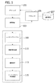
ここで図面を参照すると、本発明の態様は、より短時間でナノトポグラフィーのフィードバックを可能にして、改善された品質制御及び/又はウェーハ歩留まりのために、ナノトポグラフィーを改善するための調整を、より短い遅延時間で認識し実施することを可能にする。図1では、ブロック図は、本発明の実施形態に係る半導体ウェーハを加工するためのシステムを示している。限定ではなく例示の目的のために、システムは、グラインダ101と、測定装置103と、関連する記憶装置107を有するプロセッサ105とを含んでいる。グラインダ101はウェーハを研削し、測定装置103は、研磨したウェーハのプロファイルを示すデータを測定する。この時点での研削したウェーハは、未エッチング、未研磨である。プロセッサ105は、測定データに基づいた研削パラメータを調節するためのフィードバックを提供するように構成される。例えば、グラインダによって次に研削されるウェーハのナノトポグラフィーを改善するために、グラインダ101の1つ以上の研削ホイールを移動することができる。
<Detailed Description of the Invention>
Referring now to the drawings, aspects of the present invention allow for nanotopography feedback in a shorter time, and adjustments to improve nanotopography for improved quality control and / or wafer yield. Can be recognized and implemented with a shorter delay time. In FIG. 1, a block diagram shows a system for processing a semiconductor wafer according to an embodiment of the present invention. For purposes of illustration and not limitation, the system includes a
代わりの実施形態では、システムは複数のグラインダ101を含んでおり、各グラインダは、図1のシステムによるさらなる加工のために、ウェーハを研削する。測定装置103は、複数のグラインダ101の各々によって研削されたウェーハのプロファイルを示すデータを測定する。プロセッサ105は、複数のグラインダ101の各々にそれぞれ対応する測定データに基づいて、複数のグラインダ101の各々にフィードバックを提供するように構成される。
In an alternative embodiment, the system includes a plurality of
図1に示された実施形態では、システムは、次のような研削後の装置---研削したウェーハをエッチングするためのエッチング装置109、エッチングしたウェーハの表面を測定するための表面測定装置111(例えば、表面平坦度測定ツール)、エッチングしたウェーハを研磨するための研磨装置113、及び研磨したウェーハのナノトポグラフィーを測定するためのナノトポグラフィー測定装置115---の1つ以上を、さらに含んでいる。例えば、適したエッチング装置109としては、Atlas社から入手可能なXS300-0100 rev Cがある。適した表面測定装置111としては、Lapmaster SFT社から入手可能なWafercom 300がある。適したポリッシング装置113としては、ドイツのPeter Wolters社から入手可能なMICROLINER(登録商標) AC 2000-P2がある。適したナノトポグラフィー測定装置115は、ADE Phase Shift社から入手可能なNANOMAPPER(登録商標)がある。グラインダ101は、研磨したウェーハについて測定されたナノトポグラフィーに基づいて、さらに調節することができる。
In the embodiment shown in FIG. 1, the system includes a post-grinding device such as: an
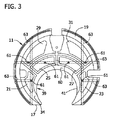
ある実施形態では、グラインダ101は、ダブルサイドグラインダである。図2は、そのようなダブルサイドグラインダのウェーハクランプデバイス201を示す。クランプデバイス201は、1組の静水圧パッド211と、1組の研削ホイール209とを含んでいる。2つの研削ホイール209は実質的に同一であり、各ホイール209は通常は平坦である。研削ホイール209と静水圧パッド211とは、互いに依存することなく半導体ウェーハW(広義には「ワークピース」)を保持しており、それぞれがクランプ面271及び273を規定する。ウェーハW上での研削ホイール209のクランプ圧(clamping pressure)は、ホイールの回転軸267に集中し、その一方、ウェーハ上での静水圧パッド211のクランプ圧は、ウェーハの中心WCの近くに集中する。
In some embodiments, the
操作中に静水圧パッド211は静止しているが、その一方で、符号241で大まかに示された駆動リングがウェーハWを動かして、パッド及び研削ホイール209に対して相対的に回転させている。図3は、典型的な静水圧パッド211を示している。静水圧パッド211(11)は、ポケット内に流体を導入するための流体注入ポート(fluid injection port)61を各々有している静水圧ポケット(hydrostatic pockets)21、23、25、27、29、31を含んでいる。パッド本体17内のチャンネル263(破線で図示)は、流体注入ポート61を相互に連結して、外部の流体源(図示せず)からポケットに流体を供給する。研削中に流体(パッド面29ではない)がウェーハWと接触するように、流体は、操作中に、比較的一定の圧力でポケット21、23、25、27、29、31の中に押し入れる。このように、ポケット21、23、25、27、29、31にある流体は、パッドのクランプ面273内にウェーハWを垂直に保持するが、潤滑されたベアリングエリア(bearing area)、又はスライドバリア(sliding barrier)も提供し、それによって、ウェーハWは、非常に低い摩擦抵抗により、研削中にパッド211に対して相対的に回転できる。パッド211のクランプ力(clamping force)は、主としてポケット21、23、25、27、29、31において提供される。
During operation, the
図2を再び参照すると、本技術分野で知られているように、駆動リング214の戻り止め(detent)又はクーポン(coupon)215が、通常は、ウェーハの周縁に形成されたノッチN(図2に破線で図示されている)の位置でウェーハWに係合して、ウェーハをその中心軸WCの周りに回転運動させる。それと同時に、(2つの)研削ホイール209がウェーハWに係合して、互いに反対方向に回転する。一方のホイール209は、ウェーハWと同じ方向に回転し、他方のホイール209は、ウェーハと反対の方向に回転する。クランプ面271及び273が研削中に同じ位置に維持される限りは、ウェーハは平面のまま(つまり、曲がらない)であり、ホイール209によって均一に研削される。
Referring back to FIG. 2, as is known in the art, a detent or
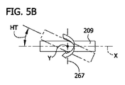
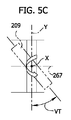
クランプ面271、273のミスアラインメントは、両面研削操作中に発生することがあり、それは一般的に、静水圧パッド211に対する研削ホイール209の移動に起因する。図4及び図5を参照すると、ミスアラインメントの3つのモード又はそれらの組合せを用いて、クランプ面271、273のミスアラインメントを特徴づけている。第1のモードでは、研削ホイールの回転軸267に沿った移動の中に、静水圧パッド211に対する研削ホイール209の横方向シフトSが存在する(図4)。第2のモードでは、それぞれの研削ホイールの中心を通る水平軸Xの周りでの、ホイール209の垂直傾斜VTが特徴である(図4及び図5)。図4は、第1のモードと第2のモードとを示している。第3のモードでは、それぞれの研削ホイール209の中心を通る縦軸Yの周りでの、ホイール209の水平傾斜HTが存在する(図5)。概念を説明するために、これらのモードは、図面中では誇張されているが、当然のことながら、実際のミスアラインメントは比較的小さいであろう。さらに、左のホイールの水平傾斜HTを右のホイールの水平傾斜と異ならせることができるように、そして、2つのホイール209の垂直傾斜VTについても同様にできるように、各ホイール209を、他方に依存せずに動かすことができる。
Misalignment of the clamp surfaces 271, 273 can occur during a double-sided grinding operation, generally due to movement of the
既に記述したように、クランプ面271、273のミスアラインメントは、ナノトポグラフィー測定装置115で測定されたときに、望ましくないナノトポグラフィーの特徴をもたらす。望ましくないナノトポグラフィーの特徴は、ウェーハの不均一な研削及び/又はウェーハの屈曲によって生じるだろう。さらに、クランプ面271、273のミスアラインメントは、研削ホイール209を不均一に摩耗させる可能性があり、そのことがさらに、ウェーハWの研削中に生じる望ましくないナノトポグラフィー特徴の発生に寄与する可能性がある。場合によっては、ウェーハは、その後の加工(例えば研磨)によって除去することのできない、望ましくない特徴を生じる可能性がある。有利なことに、本発明は、クランプ面のミスアラインメントを最小化する。特に、研削ホイール209は、ナノトポグラフィー測定装置115によって望ましくないナノトポグラフィーの特徴が検出されるまで待つのではなく、測定装置103によって研削したウェーハから得られたデータに基づいて、プロセッサ105で調節される。
As already described, misalignment of the clamping surfaces 271, 273 results in undesirable nanotopographic features as measured by the
ある実施形態では、測定装置103は、プロセッサ105と連動するように構成されたゆがみ測定装置103である。半導体ウェーハメーカーに用いられているように、ゆがみ測定装置103は、ウェーハのゆがみデータを取得し(例えば、検知し)、そのゆがみデータに基づいてウェーハのゆがみを測定する。ある実施形態では、ゆがみ測定装置103は、ゆがみデータを得るための1つ以上の容量性センサを含んでいる。得られたゆがみデータは、支持されたウェーハのプロファイル(例えばウェーハ形状)を示す。
In some embodiments, the
例えば、ゆがみ測定装置103は、図6に示されるようなライン走査プロセスを実行してもよい。このライン走査プロセスでは、ウェーハWは、ウェーハの第1の表面605に接触する1つ以上の支持ピン603に支持される。無重力状態のウェーハの形状(符号607で示されている)と、支持された状態のウェーハの形状(符号609で示されている)との間の比較によって示されているように、支持されたウェーハの形状609は、重力の関数及びウェーハWの質量により反らされる。ゆがみ測定装置103は、第1のセンサ621Aと第1の表面605A(例えば前面)との間の複数の距離(例えば「距離B」)を、支持されたウェーハ609の直径に沿って測定するための第1の静電容量センサ621Aを含んでいる。同様に、ゆがみ測定装置103は、第2のセンサ621Bと第2の表面605B(例えば裏面)との間の複数の距離(例えば「距離F」)を、支持されたウェーハ609の直径に沿って測定するための第2の静電容量センサ621Bを含んでいる。得られたゆがみデータは、直径に対応するライン走査データセットを含んでいる。ライン走査データセットは、第1のセンサ621Aで、支持されたウェーハ609の直径に沿って測定された複数の距離と、第2のセンサ621Bで、支持されたウェーハ609の直径に沿って測定された複数の距離と、を含む。ライン走査データセットは、直径に沿ったウェーハプロファイルを示す。
For example, the
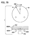
図7A及び図7Bは、複数のライン走査データセットを得るためのゆがみ測定装置103によって実行されたライン走査プロセスを示しており、各データセットは、特定の直径に沿ったウェーハプロファイルを示す。図7Aに示されているように、第1のライン走査(矢印701で示す)は、ウェーハの第1の直径に沿って実行される。特に、第1のセンサ621Aは、第1の表面605Aの上側の面内を、ウェーハの第1の直径に沿った第1の方向に移動する。第1のセンサ621Aは、第1のセンサ621Aとウェーハの第1の表面605Aとの間の距離を、所定の間隔(つまり、ピッチR、測定周波数)で測定する。あらかじめ規定された距離は、図7AのウェーハWの表面にマークを有しているものとして示されている。例えば、第1のセンサ621Aは、ウェーハの第1の直径に沿って1mm又は2mmの間隔で距離を測定してもよい。同様に、第2のセンサ621Bは、第2の表面605Bの下側の面内を第1の方向に移動して、第2のセンサ621Bと第2の表面605Bとの間の距離を、ウェーハの第1の直径に沿って測定する。ウェーハの第1の直径は、基準点の関数として規定されてもよい。例えば、図示されたプロセスでは、第1の直径は、ウェーハの周縁に設けられたノッチNを通過する。
7A and 7B show the line scanning process performed by the
図7Bに示されているように、第1のライン走査701の完了後にウェーハWを回転する(矢印709で示す)。特に、支持ピン603の下側に位置した回転ステージ705を上昇して、ウェーハWを支持ピン603より上側の位置(符号707で示す)までリフトする。回転ステージは、ウェーハをリフト位置707に支持しながら回転する。その結果、ウェーハはいくらかの角度(θ)だけ回転する。回転ステージ705が下降して、回転したウェーハは、支持ピン603の上に再度置かれる。ウェーハの第2の表面に対する支持ピン603の位置は、図7A及び図7Bに破線で示されている。次には、ウェーハの第2の直径に沿ったライン走査(矢印715で示す)が実行される。図示したプロセスによれば、第1のセンサ621A及び第2のセンサ621Bは、第1の表面605A及び第2表面605Bのぞれぞれと対応する面中を、ウェーハの第2の直径に沿った第2の方向(例えば、第1の方向と反対の方向)に移動する。第1のライン走査701に関連して上に説明したように、第1のセンサ621A及び第2のセンサ621Bは、第1のセンサ621A、第2のセンサ621Bと、ウェーハの第1の表面605A、第2表面605Bとの間の距離を、ウェーハの第2の直径に沿って、あらかじめ規定された間隔で、それぞれ測定する。複数のライン走査データセットの各々を得るために、回転709とライン走査の作業701、705とが繰り返される。
As shown in FIG. 7B, the wafer W is rotated after the completion of the first line scan 701 (indicated by arrow 709). In particular, the
ある実施形態では、ゆがみ測定装置103は、自己質量補償アルゴリズム(self mass compensation algorithm)を用いて、無重力状態607でのウェーハ形状を決定する。自己質量補償は、(複数の)ライン走査データセット、ウェーハ密度、弾性定数、ウェーハの直径及び支持ピン603の位置の関数として、ウェーハの形状を決定する。ある実施形態では、ゆがみ測定装置103は、ウェーハ形状に基づいて1つ以上のウェーハパラメータを測定する。ウェーハパラメータには、ワープ(warp)、バウ(bow)、TTV(total thickness variation:全厚み変化量)及び/又はGBIR(global back surface ideal range:グローバル裏面理想範囲)のうちの1つ以上を含むことができる。図8Aを参照すると、ワープ及びバウは、通常は基準面に対して決定される。基準面は、(複数の)支持ピン603とウェーハの表面605Aとの間の(複数の)接点の関数として規定される。具体的には、ワープは、基準面からの平均領域(median area)の最大偏差(maximum deviation)と最少偏差(minimum deviation)との間の差の絶対値として規定される。平均領域は、ウェーハの前面605Bとウェーハの裏面605Aとから等距離にある点の軌跡(locus)である。バウは、ウェーハ中心での基準面からの偏差の量として定義される。図8Bを参照すると、GBIR及びTTVは、ウェーハの線形の厚さ変化量(linear thickness variation)を反映しており、ウェーハの裏面から基準面までの最大距離と最小距離との間の差に基づいて計算することができる。
In some embodiments, the
図1に図示されたシステムを再び参照すると、グラインダ101によって研削されたままのウェーハのゆがみを測定するためのゆがみ測定装置103により得られたデータは、プロセッサ105に伝達される。例えば、ライン走査データセット及び/又は決定したウェーハ形状が、プロセッサ105に伝達されてもよい。プロセッサ105は、ゆがみデータを受信し、そして、受信したゆがみデータ処理のために複数の作業を行うコンピュータ実行可能命令(computer-executable instructions)を実行する。特に、プロセッサ105は、受信したゆがみデータに基づいてウェーハのナノトポグラフィーを予測し、そして予測されたウェーハのナノトポグラフィーに基づいて研削パラメータを決定する。グラインダ101の操作は、適宜調節される。ある実施例では、プロセッサ105は、1つ以上のソフトウェアアプリケーション、アプリケーション又はソフトウェア内のコンポーネント、実行可能ライブラリファイル(executable library file)、実行可能アプレット(executable applets)等によって具体化されたコンピュータ実行可能命令を実行するだろう。プロセッサ105に付随した(associated with)記憶装置107は、プロセッサ105がアクセスするための情報とデータと記憶する。例えば、記憶装置107は、例えばソフトウェア、アプリケーション、データ等のプロセッサ105が使用するデータ又はプロセッサ105がアクセスするデータを記憶してもよい。
Referring back to the system illustrated in FIG. 1, the data obtained by the
ある実施形態では、記憶装置107は、揮発性メディア又は不揮発性メディア(volatile or nonvolatile media)、リムーバブルメディア又はリムーバブルでないメディア(removable and non-removable media)及び/又は、コンピュータ又はコンピュータの集合体(図示せず)がアクセスできる入手可能なメディア(any available medium)であろう。限定ではなく例示として、コンピュータ読取り可能メディアは、コンピュータ記憶メディアを含んでいる。情報を記憶するための方法又は技術におけるコンピュータ記憶メディアは、例えばコンピュータ読取り可能命令、データ構造、プログラムモジュール又は他のデータなどである。例えば、コンピュータ記憶装置メディアは、RAM、ROM、EEPROM、フラッシュメモリ若しくは他のメモリ技術、CD−ROM、デジタル多用途ディスク(DVD)若しくは他の光学ディスク記憶、磁気カセット、磁気テープ、磁気ディスク記憶若しくは他の磁気記憶装置、又は所望の情報を記憶するために用いられてコンピュータにアクセスされるその他の媒体を含んでいる。
In some embodiments, the
ある実施形態では、プロセッサ105と記憶装置107は、1つ以上のコンピュータデバイスに組み入れられてもよい。当業者に知られているように、コンピュータデバイスは、プロセッサ105、1つ以上のコンピュータ読取り可能メディア、コンピュータデバイス内の様々な構成部品と接続した内部バスシステム(internal bus system)、入出力装置、ネットワークデバイス及びその他の装置の組合せを含んでいる。典型的なコンピュータデバイスは、パーソナルコンピュータ(PC)、ワークステーション、デジタルメディアプレイヤー及びその他のデジタルデバイスのうちの1つ又はそれらの組合せを含んでいる。別の実施形態では、プロセッサ105は、ネットワークを経由して、記憶装置107に記憶されたデータにアクセスする。
In certain embodiments,
ある実施形態では、プロセッサ105は、受信したゆがみデータを処理するために、フィードバックプログラムにアクセスする。受信したゆがみデータが、研削したウェーハのライン走査データセット及び/又は決定したウェーハ形状を含んでいてもよい。特に、プロセッサ105は、受信したゆがみデータに基づいて、ウェーハのナノトポグラフィーを予測する。測定装置103でウェーハを測定するときに、ウェーハはまだ研磨が行われていないことから、ウェーハのナノトポグラフィーは、実際に測定されるというよりは、むしろ予測される、といえる。上述のように、現在のナノトポグラフィー測定装置は、研磨状態にされるべきの測定されたウェーハを頼りにする技術を利用している。プロセッサ105は、予測されたウェーハのナノトポグラフィーに基づいて、1つ以上の研削パラメータを決定する。ある実施形態では、プロセッサ105は、シフトパラメータを決定する。シフトパラメータは、研削ホイール209のミスアラインメントに起因するナノトポグラフィー低下を低減するために、1組の研削ホイール209を移動させる大きさ及び方向を示している。別の実施形態では、プロセッサ105は、追加で又はその代わりに、傾斜パラメータ(tilt parameters)を決定する。傾斜パラメータは、研削ホイール209のミスアラインメントに起因するナノトポグラフィー低下を低減するために、ウェーハに対して1組の研削ホイールを位置決めする角度を示す。
In some embodiments, the
グラインダ101の操作は、決定した研削パラメータに基づいて調節される。例えば、研削ホイールは、決定した移動及び/又は傾斜パラメータで特定されているように調節されてもよい。ある実施形態では、研削ホイール209は、決定したシフト及び/又は傾斜パラメータの関数として、及びあらかじめ規定された補償量の関数として、調節される。ある実施形態では、グラインダ101は、決定した研削パラメータを受信し、決定した研削パラメータの関数としてグラインダ101の1つ以上の構成部品を調節するように、構成される。別の実施形態では、決定した研削パラメータがオペレーターに提供され、オペレーターは、決定した研削パラメータの関数としてグラインダ101の1つ以上の構成部品を調節するように、グラインダ101を構成する。
The operation of the
図9Aと図9Bは、本発明の実施形態に係る典型的なウェーハ加工方法を示している。符号903において、グラインダ101はウェーハを研削する。符号905において、研削したウェーハが第1のウェーハであるかどうか、が判断される。研削したウェーハが第1のウェーハであることが確定した場合、符号907において、測定装置103は、第1のウェーハのゆがみ及び/又は厚さを測定するためのデータを取得する。例えば、測定装置103は、図10に図示されるような4つのライン走査データセットを取得してもよい。各ライン走査データセットは、ウェーハの直径のプロファイルを示す。
9A and 9B illustrate an exemplary wafer processing method according to an embodiment of the present invention. At 903, the
図9Aに示された符号909〜915を参照すると、プロセッサ105は、第1のウェーハについて予測されたナノトポグラフィーのプロファイルを計算する作業を行う。具体的には、符号909において、プロセッサ105は、測定装置103で測定されたゆがみデータ(例えばライン走査データセット)をレベリング(level)する。ある実施形態では、測定されたゆがみデータは、規定された移動窓(defined moving window)内で最小二乗フィットを用いてレベリングされる。符号911において、プロセッサ105は、レベリングされたデータの関数として第1のプロファイルを計算するように、構成される。具体的には、レベリングされたデータは、規定された窓寸法を備えた第1のフィルタ(例えばローパスフィルタ)を用いてスムージング(smoothed)される。符号913において、第2のプロファイルは、レベリングされたデータの関数として計算される。具体的には、レベリングされたデータは、規定された窓寸法を備えた第2のフィルタを用いてフィルタリングされる。第2のフィルタは、ナノトポグラフィーではない波長(non-nanotopography wavelengths)を実質的に除去するために機能する。符号915において、ウェーハについて予測されたナノトポグラフィーのプロファイルは、計算された第1及び第2のプロファイルの関数として計算される。ある実施形態では、予測されたNTプロファイルは、第1のプロファイルから第2のプロファイルを減算することにより計算される。
Referring to reference numerals 909-915 shown in FIG. 9A, the
本発明の態様によれば、プロセッサ105は、符号909〜915の作業を繰り返して、測定装置103により得られたライン走査データセットごとに、予測された直径のナノトポグラフィーのプロファイルを計算する。図10に示した実施例では、4つの予測された直径のNTプロファイルが計算される。4つの予測された直径のNTプロファイルの各々は、4つのライン走査データセットのうちの1つから計算される。8つの予測された半径方向のNTプロファイルが、4つの予測された直径のNTプロファイルから決定される。8つの予測された半径方向のプロファイルの各々は、ウェーハの半径(例えば、0〜150mmの範囲)に沿った複数の位置における、予測されたNT高さデータを表わしている。予測された半径方向の平均NTプロファイルは、8つの予測された半径方向のプロファイルごとの予測されたNT高さデータを、半径の関数として平均することによって、計算される。図11は、ゆがみデータから得られた、予測された研削後の半径方向の平均NTプロファイルと、ナノトポグラフィー測定装置により得られた研磨後のNTプロファイルと、を比較したグラフである。
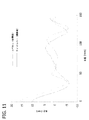
According to an aspect of the present invention, the
図9Bは、予測されたNTプロファイル(例えば、予測した半径方向の平均NTプロファイル)に基づいて研削パラメータを決定するために、プロセッサ105によって実行される作業を図示する。具体的には、図示された作業は、シフトパラメータを決定するために予測されたNTプロファイルに適用されるファジー論理アルゴリズムを表わしている。シフトパラメータは、研削ホイール209のシフトを示す方向成分と大きさ成分とを有している。以下にさらに詳細に説明する作業によれば、研削パラメータは、予測されたNTプロファイルのBリング領域に基づいて決定される。Bリング領域とは、半径が100mm〜150mmの間にあるウェーハの領域を指している。Bリング値(B-Ring value)とは、予測された半径方向の平均NTプロファイルにおける、Bリング領域内での最大ピークバレー値(maximum peak-to-valley value)を指している。一般に、より低いBリング値(例えば5nm未満)が、より望ましいナノトポグラフィーに対応する。図12は、予測された平均NTプロファイルのBリング領域に基づいてシフトパラメータを決定するために用いられる典型的なアルゴリズムを示している。図13は、予測された平均NTプロファイルを、ウェーハのBリング用に実測されたNTプロファイルと比較したグラフである。別の実施形態では、Eマークを最適化するために、同様の方法が行われる(図示せず)。Eマーク領域とは、Bリング領域と同様に、半径が100mm〜150mmの間にあるウェーハの領域を指している。Eマーク値(E-Mark value)とは、(予測された半径方向の平均NTプロファイルというよりは)予測されたNTプロファイルの各々から決定した最大ピークバレー値を指している。さらに別の実施形態では、Cマークを最適化するために、同様の方法が行われる(図示せず)。Cマーク領域とは、半径が0mm〜50mmの間にあるウェーハの領域を指している。Cマーク値(C-Mark value)とは、予測された半径方向の平均NTプロファイルにおける、Cマーク領域内での最大ピークバレー値を指している。図14は、予測された平均NTプロファイルを、Cマーク領域用に実測されたNTプロファイルと比較したグラフである。図15は、Bリング及びCマークの領域を示すウェーハ表面の典型的なトポグラフィーマップである。
FIG. 9B illustrates the operations performed by the
図9Bを再び参照すると、符号921において、プロセッサ105は、予測されたNTプロファイルのBリング値を決定する。符号923において、プロセッサ105は、Bリング値が、低く(つまり5nm)規定されたBリング値未満であるかどうかを判断する。Bリング値が低い場合、プロセッサ105は、符号925において、調整が不要である(つまり、研削パラメータの値がゼロである)、と決定する。あるいは、Bリング値が低くない(つまり5nm以上)場合、最適化サイクルが開始され、そしてこのウェーハは、最適化サイクルにおける第1のウェーハになる。最適化サイクルは、このウェーハのために、図の方法のうち後述する残りの作業を実行し、そして、その後のウェーハのために、前述の作業を繰り返す。研削パラメータに従ってグラインダで研削されたその後のウェーハが、規定された低い値(つまり5nm)より低くなったと判断されたBリング値を有するようになるまで、最適化サイクルが繰り返される。
Referring again to FIG. 9B, at
最適化サイクルによれば、プロセッサ105は、Bリング領域内の予測されたNTプロファイルに基づいて予備的なシフト方向を決定する。符号931を参照すると、プロセッサ105は、予測されたNTプロファイルが、Bリング領域内においてバレー(谷)に続いてピーク(山)(「VPプロファイル」と呼ばれる)を有する(have a valley followed by a peak)かどうか、を判断する。予測されたNTプロファイルが、Bリング領域内においてバレーに続いてピークを有すると判断された場合、研削ホイール209の予備的なシフト方向は右になる。符号933を参照すると、プロセッサ105は、予測されたNTプロファイルが、Bリング領域内においてピークに続いてバレー(「PVプロファイル」と呼ばれる)を有するかどうか、を同様に判断する。予測されたNTプロファイルが、Bリング領域内においてピークに続いてバレーを有すると判断された場合、研削ホイール209の予備的なシフト方向は左になる。
According to the optimization cycle, the
予備的なシフト方向を決定した後、プロセッサ105は、Bリング値に基づいてシフト量(shift magnitude)を決定する。符号941において、プロセッサ105は、ウェーハが最適化サイクルにおける第1のウェーハであるかどうか判断する。このウェーハが、最適化サイクルにおける第1のウェーハであると判断された場合、プロセッサ105は、所定のガイドラインに基づいて、グラインダで研削されたその後のウェーハ(つまり第2のウェーハ)の研削に用いるためのシフト量を決定する。ある実施形態では、所定のガイドラインは複数のBリング値の範囲を含んでおり、その各々は、特定のシフト量の値に関連している。グラインダ101でその後に研削されるウェーハのナノトポグラフィーを改善するために、特定のシフト量の値が選択される。図の方法によれば、符号943において、プロセッサ105は、Bリング値が18nm以上であるかどうかを判断する。Bリング値が18nm以上であると判断された場合、シフト量は15μmであり、そしてシフト方向は、決定した予備的なシフト方向になる。符号945において、プロセッサ105は、Bリング値が8nmより大きく18nm以下であるかどうかを判断する。Bリング値が8nmより大きく18nm以下であると判断された場合、シフト量は10μmであり、そしてシフト方向は、決定した予備的なシフト方向になる。符号947において、プロセッサ105は、Bリング値が5nmより大きく8nm以下であるかどうかを判断する。Bリング値が5nmより大きく8nm以下であると判断された場合、シフト量は1μmであり、そしてシフト方向は、決定した予備的なシフト方向になる。
After determining the preliminary shift direction, the
プロセッサ105が、符号941において、このウェーハは最適化サイクルにおける第1のウェーハではないと判断した場合、プロセッサ105は、符号951において、最適化プログラムを実行して、次のウェーハを研削するのに用いられるシフトパラメータを決定する。特に、最適化サイクルにおける第(n)番目のウェーハを確認し、そして、次の第(n+1)番目のウェーハ用のシフトパラメータを、第n番目のウェーハに対するBリング値と対応するシフトパラメータ値との関数として決定する。ある実施形態では、第n番目のウェーハに対するBリング値と対応するシフトパラメータとは、(n−1)次の多項式フィットティングを用いてフィッティングされる。第n番目のウェーハを用いて決定したシフトパラメータは、Bリング値がゼロ(0)のときの多項式の値に対応する。
If the
図に示されているように、本発明の態様を具体化する典型的な方法によるプロセスは、符号943、945、947又は951でシフトパラメータを決定した後に、符号903に戻る。同様に、符号925において、グラインダ101の調整が不要であるとプロセッサ105が判断した場合、最適化サイクルが終了し、方法は903に戻る。符号903において、グラインダ101は、決定した研削パラメータ(例えば、決定したシフトパラメータ)に従って、次のウェーハを研削する。符号905において、プロセッサ105は、次のウェーハが第1のウェーハであるかどうかを判断する。次のウェーハは第1のウェーハではないので、プロセッサ105は、符号961において、下記の1つ以上の条件が正しいかどうかを判断する。
・前のウェーハのBリングは、所定の値(例えば8nm)より大きい。
・カセット番号は、測定装置103によって最後に測定されたウェーハ用のカセットよりも2つ大きい。1つ以上の条件が正しい場合、測定装置103は、上述した実施方法の符号907において、ウェーハのゆがみデータを取得する。いずれの条件も正しくない場合、そのウェーハに対して図示した方法のウェーハの次の工程(wafer subsequent steps)は行われず、そして本方法は、その後のウェーハを研削するための工程903に戻す。
As shown in the figure, an exemplary method process embodying aspects of the present invention returns to reference numeral 903 after determining shift parameters at
The B ring of the previous wafer is greater than a predetermined value (eg 8 nm).
The cassette number is two larger than the wafer cassette last measured by the measuring
本発明又はその好ましい実施形態の要素を導入するときに、冠詞の「ある("a", "an")」、「前記("the", "said")」は、1つ以上の要素が存在することを意味するように意図している。用語の「含む("comprising")」、「含む("including")」、「有する("having")」は、記載された要素以外の追加の要素が存在しうることを含み且つ意味するように意図している。 When introducing elements of the present invention or preferred embodiments thereof, the articles “a”, “an”), “the” “sai”, “said” ”have one or more elements It is intended to mean to exist. The terms “comprising”, “including”, “having” include and mean that there may be additional elements other than the listed elements. Is intended.
発明の範囲から逸脱することなく上記の方法に様々な変更を行なうことができるとともに、上記の説明に含まれそして添付の図面に図示された全ての事項は、例示として解釈されるべきであり、制限する意味ではないことを意図している。 Various modifications can be made to the above method without departing from the scope of the invention, and all matters included in the above description and illustrated in the accompanying drawings are to be construed as illustrative, It is not meant to be limiting.
Claims (24)
前記方法は、
前記ダブルサイドグラインダによって研削されたままのウェーハのゆがみを測定するためのゆがみ測定装置により得られたデータを受信する工程であって、受信したゆがみデータは、測定された前記ゆがみを示している、データ受信工程と、
受信した前記ゆがみデータに基づいて、前記ウェーハのナノトポグラフィーの予測する工程と、
予測された前記ウェーハの前記ナノトポグラフィーに基づいて、研削パラメータを決定する工程と、
決定した前記研削パラメータに基づいて、前記ダブルサイドグラインダの操作を調節する工程と、を含むことを特徴とするウェーハ加工方法。 A method of processing a wafer using a double side grinder, wherein the double side grinder has at least one set of grinding wheels,
The method
Receiving the data obtained by the distortion measuring device for measuring the distortion of the wafer that has been ground by the double-side grinder, wherein the received distortion data indicates the measured distortion; A data receiving process;
Predicting the nanotopography of the wafer based on the received distortion data;
Determining grinding parameters based on the predicted nanotopography of the wafer;
Adjusting the operation of the double side grinder based on the determined grinding parameter.
前記フィードバックは、決定した前記研削パラメータを含むことを特徴とする請求項1に記載の方法。 Adjusting the operation of the double side grinder includes providing feedback to the double side grinder;
The method of claim 1, wherein the feedback includes the determined grinding parameters.
前記シフトパラメータは、前記ダブルサイドグラインダによってその後に研削されるウェーハのナノトポグラフィーを改善するために、前記1組の研削ホイールを移動させる大きさを示していることを特徴とする請求項1に記載の方法。 The step of determining includes determining a shift parameter based on the predicted nanotopography of the wafer;
The shift parameter indicates a magnitude by which the set of grinding wheels is moved to improve nanotopography of a wafer that is subsequently ground by the double side grinder. The method described.
前記シフトパラメータは、前記ダブルサイドグラインダによってその後に研削されるウェーハのナノトポグラフィーを改善するために、前記1組の研削ホイールを移動させる方向を示していることを特徴とする請求項1に記載の方法。 The step of determining includes determining a shift parameter based on the predicted nanotopography of the wafer;
The shift parameter indicates a direction in which the set of grinding wheels are moved to improve nanotopography of a wafer that is subsequently ground by the double side grinder. the method of.
前記予測する工程が、フィルタリングされた前記ゆがみデータに基づいて、前記ウェーハの前記ナノトポグラフィーを予測する過程を含んでいることを特徴とする請求項1に記載の方法。 Further comprising filtering the received distortion data;
The method of claim 1, wherein the step of predicting includes predicting the nanotopography of the wafer based on the filtered distortion data.
前記決定する工程は、計算された前記プロファイルのBリング領域に基づいて、研削パラメータを決定する過程を含むことを特徴とする請求項1に記載の方法。 The step of predicting includes calculating a profile of the surface of the wafer;
The method of claim 1, wherein the determining step includes determining grinding parameters based on the calculated B-ring region of the profile.
研磨後の前記ウェーハのナノトポグラフィーを測定する工程と、をさらに含むことを特徴とする請求項1に記載の方法。 Polishing the wafer;
The method of claim 1, further comprising: measuring the nanotopography of the wafer after polishing.
前記方法は、
前記ダブルサイドグラインダによって研削されたままのウェーハのプロファイルを示すデータを受信する工程と、
ファジー論理アルゴリズムを実行して、受信した前記データの関数として研削パラメータを決定する工程と、
前記ダブルサイドグラインダの操作を調節するために、前記ダブルサイドグラインダに、決定した前記研削パラメータを含むフィードバックを提供する工程と、を含むことを特徴とするコンピュータで実施される方法。 A computer implemented method for improving the nanotopography of a wafer ground by a double side grinder, said double side grinder having at least one set of grinding wheels;
The method
Receiving data indicative of the profile of the wafer as ground by the double side grinder;
Performing a fuzzy logic algorithm to determine grinding parameters as a function of the received data;
Providing the double side grinder with feedback including the determined grinding parameters to adjust the operation of the double side grinder.
前記シフトパラメータは、前記ダブルサイドグラインダによってその後に研削されるウェーハのナノトポグラフィーを改善するために、前記1組の研削ホイールを移動させる大きさを示していることを特徴とする請求項11に記載のコンピュータで実施される方法。 The step of determining includes determining a shift parameter based on the predicted nanotopography of the wafer;
12. The shift parameter indicates a magnitude of moving the set of grinding wheels to improve nanotopography of a wafer that is subsequently ground by the double side grinder. A computer-implemented method as described.
前記シフトパラメータは、前記ダブルサイドグラインダによってその後に研削されるウェーハのナノトポグラフィーを改善するために、前記1組の研削ホイールを移動させる方向を示していることを特徴とする請求項11に記載のコンピュータで実施される方法。 The step of determining includes determining a shift parameter based on the predicted nanotopography of the wafer;
The shift parameter indicates a direction in which the set of grinding wheels are moved to improve nanotopography of a wafer that is subsequently ground by the double side grinder. Computer-implemented method.
前記ウェーハは、未エッチング及び未研磨であることを特徴とする請求項11に記載のコンピュータで実施される方法。 The step of receiving includes a step of receiving data obtained by a distortion measuring device for measuring distortion of a wafer ground by the double side grinder,
The computer-implemented method of claim 11, wherein the wafer is unetched and unpolished.
前記ウェーハは、未エッチング及び未研磨であることを特徴とする請求項11に記載のコンピュータで実施される方法。 The receiving step includes a step of receiving data obtained by a measuring device for measuring a thickness of a wafer ground by the double side grinder,
The computer-implemented method of claim 11, wherein the wafer is unetched and unpolished.
前記システムは、
ウェーハを研削するための1組のホイールを有するダブルサイドグラインダと、
研削した前記ウェーハのプロファイルを示すデータを測定するための測定装置と、
ファジー論理アルゴリズムを実行して、測定した前記データの関数として研削パラメータを決定するように構成されたプロセッサと、を含み
前記ダブルサイドグラインダの前記ホイールの少なくとも1つは、決定した前記研削パラメータに基づいて調節されることを特徴とするシステム。 A system for processing a semiconductor wafer,
The system
A double side grinder having a set of wheels for grinding the wafer;
A measuring device for measuring data indicating the profile of the ground wafer;
A processor configured to execute a fuzzy logic algorithm to determine grinding parameters as a function of the measured data, wherein at least one of the wheels of the double side grinder is based on the determined grinding parameters System characterized by being adjusted.
前記プロセッサは、ファジー論理アルゴリズムを実行して、測定した前記ゆがみデータの関数として研削パラメータを決定するように構成されたプロセッサであることを特徴とする請求項17に記載のシステム。 The measuring device is a distortion measuring device for obtaining distortion data from the ground wafer, and the ground wafer is unetched and unpolished,
The system of claim 17, wherein the processor is a processor configured to execute a fuzzy logic algorithm to determine grinding parameters as a function of the measured distortion data.
研削した前記ウェーハは、未エッチング及び未研磨であることを特徴とする請求項17に記載のシステム。 The measuring device includes a capacitive sensor for measuring data indicative of the profile of the ground wafer;
The system of claim 17, wherein the ground wafer is unetched and unpolished.
エッチングした前記ウェーハを研磨するための研磨装置と、
研磨した前記ウェーハのナノトポグラフィーを測定するためのナノトポグラフィー測定装置と、をさらに含むことを特徴とする請求項17のシステム。 An etching apparatus for etching the ground wafer;
A polishing apparatus for polishing the etched wafer;
The system of claim 17, further comprising a nanotopography measurement device for measuring the nanotopography of the polished wafer.
前記シフトパラメータは、前記ダブルサイドグラインダによってその後に研削されるウェーハのナノトポグラフィーを改善するために、前記1組の研削ホイールを移動させる大きさを示していることを特徴とする請求項17に記載のシステム。 The processor is a processor configured to execute a fuzzy logic algorithm to determine a shift parameter as a function of the measured data;
18. The shift parameter indicates a magnitude of moving the set of grinding wheels to improve nanotopography of a wafer that is subsequently ground by the double side grinder. The described system.
前記シフトパラメータは、前記ダブルサイドグラインダによってその後に研削されるウェーハのナノトポグラフィーを改善するために、前記1組の研削ホイールを移動させる方向を示していることを特徴とする請求項17に記載のシステム。 The processor is a processor configured to execute a fuzzy logic algorithm to determine a shift parameter as a function of the measured data;
18. The shift parameter indicates a direction in which the set of grinding wheels are moved to improve nanotopography of a wafer that is subsequently ground by the double side grinder. System.
前記測定装置は、研削した前記ウェーハの第1のプロファイルを示すデータと、研削した前記別のウェーハの別のプロファイルを示すデータと、を測定するための1つの測定装置であり、
前記プロセッサは、ファジー論理アルゴリズムを実行して、前記第1のプロファイルを示している測定した前記データの関数として研削パラメータを決定するように、及び前記ファジー論理アルゴリズムを実行して、前記別のプロファイルを示している測定した前記データの関数として前記研削パラメータを決定するように、構成されていることを特徴とする請求項17に記載のシステム。 A second double grinder having a set of wheels for grinding another wafer;
The measuring device is one measuring device for measuring data indicating a first profile of the ground wafer and data indicating another profile of the ground another wafer;
The processor executes a fuzzy logic algorithm to determine grinding parameters as a function of the measured data indicative of the first profile, and executes the fuzzy logic algorithm to execute the another profile. The system of claim 17, wherein the system is configured to determine the grinding parameter as a function of the measured data indicative of
Applications Claiming Priority (2)
| Application Number | Priority Date | Filing Date | Title |
|---|---|---|---|
| US11/967,743 US7930058B2 (en) | 2006-01-30 | 2007-12-31 | Nanotopography control and optimization using feedback from warp data |
| PCT/US2008/088452 WO2009088832A1 (en) | 2007-12-31 | 2008-12-29 | Nanotopography control and optimization using feedback from warp data |
Publications (2)
| Publication Number | Publication Date |
|---|---|
| JP2011507719A true JP2011507719A (en) | 2011-03-10 |
| JP2011507719A5 JP2011507719A5 (en) | 2011-05-26 |
Family
ID=40538746
Family Applications (1)
| Application Number | Title | Priority Date | Filing Date |
|---|---|---|---|
| JP2010540928A Pending JP2011507719A (en) | 2007-12-31 | 2008-12-29 | Control and optimization of nanotopography using feedback from distortion data |
Country Status (7)
| Country | Link |
|---|---|
| US (2) | US7930058B2 (en) |
| EP (1) | EP2225070B1 (en) |
| JP (1) | JP2011507719A (en) |
| KR (1) | KR20100110803A (en) |
| CN (1) | CN101909817A (en) |
| TW (1) | TWI446992B (en) |
| WO (1) | WO2009088832A1 (en) |
Cited By (3)
| Publication number | Priority date | Publication date | Assignee | Title |
|---|---|---|---|---|
| KR20150084764A (en) * | 2012-11-13 | 2015-07-22 | 신에쯔 한도타이 가부시키가이샤 | Double-sided polishing method |
| JP2016505214A (en) * | 2012-12-28 | 2016-02-18 | サンエディソン・セミコンダクター・リミテッドSunEdison Semiconductor Limited | Method for predicting and controlling post-epitaxial warpage |
| JP6443520B1 (en) * | 2017-10-02 | 2018-12-26 | 株式会社Sumco | Semiconductor wafer evaluation method and semiconductor wafer manufacturing method using the method |
Families Citing this family (30)
| Publication number | Priority date | Publication date | Assignee | Title |
|---|---|---|---|---|
| KR101141474B1 (en) * | 2004-03-19 | 2012-05-07 | 엠이엠씨 일렉트로닉 머티리얼즈, 인크. | Wafer clamping device for a double side grinder |
| US7544112B1 (en) * | 2006-12-13 | 2009-06-09 | Huffman Corporation | Method and apparatus for removing coatings from a substrate using multiple sequential steps |
| US8221199B2 (en) * | 2007-01-11 | 2012-07-17 | Smith Abrasives, Inc | Abrasive sharpener |
| DE102007056628B4 (en) * | 2007-03-19 | 2019-03-14 | Siltronic Ag | Method and apparatus for simultaneously grinding a plurality of semiconductor wafers |
| US8214178B2 (en) * | 2008-06-04 | 2012-07-03 | Vibration Technologies, Llc | Method and system for optimizing the vibrational characteristics of a structure |
| US8360817B2 (en) * | 2009-04-01 | 2013-01-29 | Ebara Corporation | Polishing apparatus and polishing method |
| DE102009024125B4 (en) * | 2009-06-06 | 2023-07-27 | Lapmaster Wolters Gmbh | Process for processing flat workpieces |
| US8883034B2 (en) * | 2009-09-16 | 2014-11-11 | Brian Reiss | Composition and method for polishing bulk silicon |
| US8815110B2 (en) * | 2009-09-16 | 2014-08-26 | Cabot Microelectronics Corporation | Composition and method for polishing bulk silicon |
| US8697576B2 (en) * | 2009-09-16 | 2014-04-15 | Cabot Microelectronics Corporation | Composition and method for polishing polysilicon |
| JP5504901B2 (en) | 2010-01-13 | 2014-05-28 | 株式会社Sumco | Polishing pad shape correction method |
| US8712575B2 (en) * | 2010-03-26 | 2014-04-29 | Memc Electronic Materials, Inc. | Hydrostatic pad pressure modulation in a simultaneous double side wafer grinder |
| JP5862492B2 (en) * | 2012-07-09 | 2016-02-16 | 信越半導体株式会社 | Semiconductor wafer evaluation method and manufacturing method |
| US9881783B2 (en) * | 2013-02-19 | 2018-01-30 | Sumco Corporation | Method for processing semiconductor wafer |
| US9375824B2 (en) * | 2013-11-27 | 2016-06-28 | Applied Materials, Inc. | Adjustment of polishing rates during substrate polishing with predictive filters |
| US9490186B2 (en) * | 2013-11-27 | 2016-11-08 | Applied Materials, Inc. | Limiting adjustment of polishing rates during substrate polishing |
| CN104108062B (en) * | 2014-06-17 | 2017-06-06 | 北京石晶光电科技股份有限公司济源分公司 | A kind of ultra thin wafer nanoscale polishing method |
| JP6447472B2 (en) * | 2015-11-26 | 2019-01-09 | 株式会社Sumco | Wafer polishing method |
| TWI779986B (en) | 2016-11-30 | 2022-10-01 | 美商應用材料股份有限公司 | Spectrographic monitoring using a neural network |
| JP6436255B1 (en) * | 2018-02-27 | 2018-12-12 | 株式会社Sumco | Method for predicting warpage of silicon wafer and method for manufacturing silicon wafer |
| CN108493116A (en) * | 2018-03-13 | 2018-09-04 | 英特尔产品(成都)有限公司 | The Place module of manufacturing method and this method manufacture of Place module |
| DE102018221922A1 (en) * | 2018-12-17 | 2020-06-18 | Siltronic Ag | Method for producing semiconductor wafers using a wire saw, wire saw and semiconductor wafer made of single-crystal silicon |
| CN110193776B (en) * | 2019-06-11 | 2020-07-03 | 英特尔半导体(大连)有限公司 | Polishing pressure control method, device and equipment for wafer polishing |
| US11415971B2 (en) | 2020-02-10 | 2022-08-16 | Globalwafers Co., Ltd. | Systems and methods for enhanced wafer manufacturing |
| TWI763112B (en) * | 2020-04-22 | 2022-05-01 | 財團法人工業技術研究院 | Grinding and polishing simulation method, system and grinding and polishing process transferring method |
| US20210331287A1 (en) * | 2020-04-22 | 2021-10-28 | Industrial Technology Research Institute | Grinding and polishing simulation method and system and grinding and polishing process transferring method |
| CN112071765A (en) * | 2020-08-18 | 2020-12-11 | 徐州鑫晶半导体科技有限公司 | Method for determining wafer processing parameters and wafer processing method |
| CN112259442A (en) * | 2020-09-11 | 2021-01-22 | 徐州鑫晶半导体科技有限公司 | Method and device for thinning double surfaces of wafer and storage medium |
| CN115194639B (en) * | 2022-06-30 | 2023-12-29 | 江西兆驰半导体有限公司 | Classification processing method for cut sapphire substrate slice and epitaxial wafer |
| CN116175397A (en) * | 2022-12-13 | 2023-05-30 | 西安奕斯伟材料科技有限公司 | Device and method for grinding silicon wafer |
Citations (1)
| Publication number | Priority date | Publication date | Assignee | Title |
|---|---|---|---|---|
| WO2007130708A1 (en) * | 2006-01-30 | 2007-11-15 | Memc Electronic Materials, Inc. | Double side wafer grinder and methods for assessing workpiece nanotopology |
Family Cites Families (69)
| Publication number | Priority date | Publication date | Assignee | Title |
|---|---|---|---|---|
| US2448751A (en) * | 1946-08-10 | 1948-09-07 | Volkel Bros Machine Works | Record edging lathe |
| KR920002268A (en) * | 1990-07-17 | 1992-02-28 | 유끼노리 가까즈 | Intelligent Processing Equipment |
| US5402354A (en) * | 1990-10-12 | 1995-03-28 | Mitsubishi Jukogyo Kabushiki Kaisha | Control apparatus and control method for machine tools using fuzzy reasoning |
| JPH0577159A (en) * | 1991-09-18 | 1993-03-30 | Mitsubishi Heavy Ind Ltd | Computing method for ground material deflection quantity of grinding machine |
| US5700180A (en) * | 1993-08-25 | 1997-12-23 | Micron Technology, Inc. | System for real-time control of semiconductor wafer polishing |
| JP3386548B2 (en) * | 1994-01-31 | 2003-03-17 | トヨタ自動車株式会社 | Feedback processing condition correction device |
| JP3702496B2 (en) * | 1995-07-10 | 2005-10-05 | 三菱電機株式会社 | Machining method using numerical controller |
| KR100227924B1 (en) | 1995-07-28 | 1999-11-01 | 가이데 히사오 | Wafer fabricating method and polishing method therefor and apparatus thereof |
| JP3620554B2 (en) * | 1996-03-25 | 2005-02-16 | 信越半導体株式会社 | Semiconductor wafer manufacturing method |
| MY121670A (en) * | 1996-09-09 | 2006-02-28 | Koyo Machine Ind Co Ltd | Double side grinding apparatus for flat disklike work |
| AU4673797A (en) * | 1996-10-04 | 1998-04-24 | Exclusive Design Company, Inc. | A method and system for controlling chemical mechanical polishing thickness removal |
| US5816895A (en) * | 1997-01-17 | 1998-10-06 | Tokyo Seimitsu Co., Ltd. | Surface grinding method and apparatus |
| EP0875809A3 (en) * | 1997-04-28 | 2000-09-06 | Seiko Seiki Kabushiki Kaisha | CAD/CAM apparatus and machining apparatus |
| JPH11198009A (en) * | 1998-01-13 | 1999-07-27 | Koyo Mach Ind Co Ltd | Double side grinding device and cross section measuring device for thin plate disk workpiece |
| JPH11254282A (en) * | 1998-03-04 | 1999-09-21 | Super Silicon Kenkyusho:Kk | Duplex grinding device and duplex polishing device |
| JP2000015557A (en) * | 1998-04-27 | 2000-01-18 | Ebara Corp | Polishing device |
| JP3292835B2 (en) * | 1998-05-06 | 2002-06-17 | 信越半導体株式会社 | Surface grinding method for thin work and its grinding device |
| US6875085B2 (en) * | 1998-11-06 | 2005-04-05 | Mosel Vitelic, Inc. | Polishing system including a hydrostatic fluid bearing support |
| US6428388B2 (en) * | 1998-11-06 | 2002-08-06 | Beaver Creek Concepts Inc. | Finishing element with finishing aids |
| JP3951496B2 (en) | 1999-03-30 | 2007-08-01 | 光洋機械工業株式会社 | Double-side grinding machine for thin disk-shaped workpieces |
| EP1118429B1 (en) | 1999-05-07 | 2007-10-24 | Shin-Etsu Handotai Co., Ltd | Method and device for simultaneously grinding double surfaces, and method and device for simultaneously lapping double surfaces |
| US6198294B1 (en) * | 1999-05-17 | 2001-03-06 | Vlsi Technology, Inc. | In-situ backgrind wafer thickness monitor |
| KR100706626B1 (en) * | 1999-09-24 | 2007-04-13 | 신에츠 한도타이 가부시키가이샤 | Method and device for grinding double sides of thin disk work |
| US6479386B1 (en) * | 2000-02-16 | 2002-11-12 | Memc Electronic Materials, Inc. | Process for reducing surface variations for polished wafer |
| US6368881B1 (en) * | 2000-02-29 | 2002-04-09 | International Business Machines Corporation | Wafer thickness control during backside grind |
| US20020052169A1 (en) * | 2000-03-17 | 2002-05-02 | Krishna Vepa | Systems and methods to significantly reduce the grinding marks in surface grinding of semiconductor wafers |
| US6852012B2 (en) * | 2000-03-17 | 2005-02-08 | Wafer Solutions, Inc. | Cluster tool systems and methods for in fab wafer processing |
| DE10023002B4 (en) * | 2000-05-11 | 2006-10-26 | Siltronic Ag | Set of carriers and its use |
| US20020086625A1 (en) * | 2000-05-23 | 2002-07-04 | Wafer Solutions, Inc. | Vacuum mount wafer polishing methods and apparatus |
| US6556884B1 (en) * | 2000-06-16 | 2003-04-29 | Advanced Micro Devices, Inc. | Method and apparatus for interfacing a statistical process control system with a manufacturing process control framework |
| KR100792774B1 (en) * | 2000-06-29 | 2008-01-11 | 신에쯔 한도타이 가부시키가이샤 | Method for processing semiconductor wafer and semiconductor wafer |
| EP1307321A2 (en) | 2000-08-07 | 2003-05-07 | MEMC Electronic Materials, Inc. | Method for processing a semiconductor wafer using double-side polishing |
| US6709981B2 (en) * | 2000-08-16 | 2004-03-23 | Memc Electronic Materials, Inc. | Method and apparatus for processing a semiconductor wafer using novel final polishing method |
| US6556876B1 (en) * | 2000-10-12 | 2003-04-29 | National Semiconductor Corporation | Hybrid fuzzy closed-loop sub-micron critical dimension control in wafer manufacturing |
| GB2368971B (en) * | 2000-11-11 | 2005-01-05 | Pure Wafer Ltd | Process for Reclaimimg Wafer Substrates |
| US6672943B2 (en) * | 2001-01-26 | 2004-01-06 | Wafer Solutions, Inc. | Eccentric abrasive wheel for wafer processing |
| JP2002307303A (en) | 2001-04-10 | 2002-10-23 | Koyo Mach Ind Co Ltd | Both face grinding method for thin plate disclike workpiece and device thereof |
| JP2002343772A (en) * | 2001-05-18 | 2002-11-29 | Speedfam Co Ltd | Local plasma etching method |
| US20020185053A1 (en) * | 2001-05-24 | 2002-12-12 | Lu Fei | Method for calibrating nanotopographic measuring equipment |
| US6594024B1 (en) * | 2001-06-21 | 2003-07-15 | Advanced Micro Devices, Inc. | Monitor CMP process using scatterometry |
| JP4876345B2 (en) * | 2001-08-22 | 2012-02-15 | 株式会社ニコン | Simulation method and apparatus, and polishing method and apparatus using the same |
| DE10142400B4 (en) * | 2001-08-30 | 2009-09-03 | Siltronic Ag | Improved local flatness semiconductor wafer and method of making the same |
| US6914000B2 (en) * | 2001-09-04 | 2005-07-05 | Matsushita Electric Industrial Co., Ltd. | Polishing method, polishing system and process-managing system |
| JP3995926B2 (en) * | 2001-09-18 | 2007-10-24 | 株式会社富士通長野システムエンジニアリング | Structure analysis program, structure analysis method, structure analysis apparatus, and semiconductor integrated circuit manufacturing method |
| US6630360B2 (en) * | 2002-01-10 | 2003-10-07 | Advanced Micro Devices, Inc. | Advanced process control (APC) of copper thickness for chemical mechanical planarization (CMP) optimization |
| DE10208165C1 (en) * | 2002-02-26 | 2003-10-02 | Advanced Micro Devices Inc | Method, control and device for controlling the chemical mechanical polishing of substrates |
| US6613591B1 (en) * | 2002-03-07 | 2003-09-02 | Memc Electronic Materials, Inc. | Method of estimating post-polishing waviness characteristics of a semiconductor wafer |
| DE10314212B4 (en) * | 2002-03-29 | 2010-06-02 | Hoya Corp. | Method for producing a mask blank, method for producing a transfer mask |
| US7363099B2 (en) * | 2002-06-07 | 2008-04-22 | Cadence Design Systems, Inc. | Integrated circuit metrology |
| JP4464033B2 (en) * | 2002-06-13 | 2010-05-19 | 信越半導体株式会社 | Semiconductor wafer shape evaluation method and shape evaluation apparatus |
| US7416962B2 (en) * | 2002-08-30 | 2008-08-26 | Siltronic Corporation | Method for processing a semiconductor wafer including back side grinding |
| US7150674B2 (en) * | 2002-10-09 | 2006-12-19 | Koyo Machine Industries Co., Ltd. | Both-side grinding method and both-side grinding machine for thin disc work |
| EP1457828A3 (en) | 2003-03-10 | 2009-04-22 | ASML Netherlands B.V. | Focus spot monitoring in a lithographic projection apparatus |
| US7118446B2 (en) * | 2003-04-04 | 2006-10-10 | Strasbaugh, A California Corporation | Grinding apparatus and method |
| TWI224037B (en) * | 2003-12-30 | 2004-11-21 | Ind Tech Res Inst | Grinder structure for wafer |
| DE102004005702A1 (en) * | 2004-02-05 | 2005-09-01 | Siltronic Ag | Semiconductor wafer, apparatus and method for producing the semiconductor wafer |
| DE102004011996B4 (en) | 2004-03-11 | 2007-12-06 | Siltronic Ag | Device for simultaneous two-sided grinding of disc-shaped workpieces |
| KR101141474B1 (en) | 2004-03-19 | 2012-05-07 | 엠이엠씨 일렉트로닉 머티리얼즈, 인크. | Wafer clamping device for a double side grinder |
| JP4163145B2 (en) * | 2004-04-30 | 2008-10-08 | 株式会社ルネサステクノロジ | Wafer polishing method |
| JP4994227B2 (en) * | 2004-06-21 | 2012-08-08 | 株式会社荏原製作所 | Polishing apparatus and polishing method |
| US7814456B2 (en) * | 2004-11-22 | 2010-10-12 | Tela Innovations, Inc. | Method and system for topography-aware reticle enhancement |
| JP2006228843A (en) * | 2005-02-16 | 2006-08-31 | Renesas Technology Corp | Process control method and manufacturing method of semiconductor device |
| US7810383B2 (en) * | 2005-04-08 | 2010-10-12 | Shin-Etsu Handotai Co., Ltd. | Method for evaluating semiconductor wafer, apparatus for evaluating semiconductor wafer, and method for manufacturing semiconductor wafer |
| US20070006652A1 (en) | 2005-07-06 | 2007-01-11 | Abnaki Systems, Inc. | Load measuring sensor and method |
| US7636611B2 (en) * | 2005-10-28 | 2009-12-22 | Samsung Austin Semiconductor, L.P. | Fuzzy logic system for process control in chemical mechanical polishing |
| US7601049B2 (en) * | 2006-01-30 | 2009-10-13 | Memc Electronic Materials, Inc. | Double side wafer grinder and methods for assessing workpiece nanotopology |
| JP2008010818A (en) * | 2006-06-01 | 2008-01-17 | Sumitomo Electric Ind Ltd | Substrate, substrate inspecting method and methods of manufacturing element and substrate |
| DE102007056628B4 (en) * | 2007-03-19 | 2019-03-14 | Siltronic Ag | Method and apparatus for simultaneously grinding a plurality of semiconductor wafers |
| JP4985451B2 (en) * | 2008-02-14 | 2012-07-25 | 信越半導体株式会社 | Double-head grinding apparatus for workpiece and double-head grinding method for workpiece |
-
2007
- 2007-12-31 US US11/967,743 patent/US7930058B2/en active Active
-
2008
- 2008-12-29 EP EP08869803.0A patent/EP2225070B1/en active Active
- 2008-12-29 WO PCT/US2008/088452 patent/WO2009088832A1/en active Application Filing
- 2008-12-29 KR KR1020107014398A patent/KR20100110803A/en not_active Application Discontinuation
- 2008-12-29 CN CN2008801235079A patent/CN101909817A/en active Pending
- 2008-12-29 JP JP2010540928A patent/JP2011507719A/en active Pending
- 2008-12-31 TW TW097151687A patent/TWI446992B/en active
-
2010
- 2010-09-27 US US12/891,357 patent/US8145342B2/en active Active
Patent Citations (1)
| Publication number | Priority date | Publication date | Assignee | Title |
|---|---|---|---|---|
| WO2007130708A1 (en) * | 2006-01-30 | 2007-11-15 | Memc Electronic Materials, Inc. | Double side wafer grinder and methods for assessing workpiece nanotopology |
Cited By (5)
| Publication number | Priority date | Publication date | Assignee | Title |
|---|---|---|---|---|
| KR20150084764A (en) * | 2012-11-13 | 2015-07-22 | 신에쯔 한도타이 가부시키가이샤 | Double-sided polishing method |
| KR102004701B1 (en) * | 2012-11-13 | 2019-07-29 | 신에쯔 한도타이 가부시키가이샤 | Double-sided polishing method |
| JP2016505214A (en) * | 2012-12-28 | 2016-02-18 | サンエディソン・セミコンダクター・リミテッドSunEdison Semiconductor Limited | Method for predicting and controlling post-epitaxial warpage |
| JP6443520B1 (en) * | 2017-10-02 | 2018-12-26 | 株式会社Sumco | Semiconductor wafer evaluation method and semiconductor wafer manufacturing method using the method |
| JP2019067952A (en) * | 2017-10-02 | 2019-04-25 | 株式会社Sumco | Evaluating method of semiconductor wafer and manufacturing method of semiconductor wafer using the method |
Also Published As
| Publication number | Publication date |
|---|---|
| TW200946284A (en) | 2009-11-16 |
| WO2009088832A1 (en) | 2009-07-16 |
| TWI446992B (en) | 2014-08-01 |
| US20110045740A1 (en) | 2011-02-24 |
| EP2225070B1 (en) | 2014-02-12 |
| US7930058B2 (en) | 2011-04-19 |
| US8145342B2 (en) | 2012-03-27 |
| EP2225070A1 (en) | 2010-09-08 |
| KR20100110803A (en) | 2010-10-13 |
| US20080166948A1 (en) | 2008-07-10 |
| CN101909817A (en) | 2010-12-08 |
Similar Documents
| Publication | Publication Date | Title |
|---|---|---|
| EP2225070B1 (en) | Nanotopography control and optimization using feedback from warp data | |
| TWI520202B (en) | Hydrostatic pad pressure modulation in a simultaneous double side wafer grinder | |
| JP6146213B2 (en) | Double-side polishing apparatus and double-side polishing method for work | |
| WO2010013390A1 (en) | Wafer polishing method and double side polishing apparatus | |
| JP6166383B2 (en) | Method for predicting and controlling post-epitaxial warpage | |
| KR100642879B1 (en) | Method and device for simultaneously grinding double surfaces, and method and device for simultaneously lapping double surfaces | |
| KR19990045021A (en) | Polishing apparatus having a wear measurement means of a pad and a method of operating the same | |
| CN104428882B (en) | Evaluation method and production method for semiconductor wafers | |
| JP2013524484A5 (en) | ||
| US10180316B2 (en) | Method and device for the contactless assessment of the surface quality of a wafer | |
| KR102041240B1 (en) | Method and apparatus of polishing single-side of single semiconductor wafer | |
| JP5028354B2 (en) | Wafer polishing method | |
| JP2004022676A (en) | Working method and plasma etching equipment of semiconductor wafer | |
| KR101247065B1 (en) | Double side wafer grinder and methods for assessing workpiece nanotopology | |
| CN108153111A (en) | Form the substrate and detection method of template | |
| JPH11245162A (en) | Tool having flat working surface | |
| JP6539467B2 (en) | Grinding machine | |
| TWI740606B (en) | Double side polishing method for workpiece | |
| WO2003107402A1 (en) | Semiconductor wafer | |
| JP5699783B2 (en) | Work polishing method and polishing apparatus | |
| JP6712841B2 (en) | Grinding method | |
| JP2007095987A (en) | Method of manufacturing semiconductor wafer and grinding apparatus |
Legal Events
| Date | Code | Title | Description |
|---|---|---|---|
| A521 | Request for written amendment filed |
Free format text: JAPANESE INTERMEDIATE CODE: A523 Effective date: 20110407 |
|
| A621 | Written request for application examination |
Free format text: JAPANESE INTERMEDIATE CODE: A621 Effective date: 20110407 |
|
| A977 | Report on retrieval |
Free format text: JAPANESE INTERMEDIATE CODE: A971007 Effective date: 20130207 |
|
| A131 | Notification of reasons for refusal |
Free format text: JAPANESE INTERMEDIATE CODE: A131 Effective date: 20130212 |
|
| A601 | Written request for extension of time |
Free format text: JAPANESE INTERMEDIATE CODE: A601 Effective date: 20130513 |
|
| A602 | Written permission of extension of time |
Free format text: JAPANESE INTERMEDIATE CODE: A602 Effective date: 20130520 |
|
| A601 | Written request for extension of time |
Free format text: JAPANESE INTERMEDIATE CODE: A601 Effective date: 20130611 |
|
| A602 | Written permission of extension of time |
Free format text: JAPANESE INTERMEDIATE CODE: A602 Effective date: 20130618 |
|
| A02 | Decision of refusal |
Free format text: JAPANESE INTERMEDIATE CODE: A02 Effective date: 20131008 |