JP2011199579A - Electronic device and method for manufacturing electronic device - Google Patents
Electronic device and method for manufacturing electronic device Download PDFInfo
- Publication number
- JP2011199579A JP2011199579A JP2010063876A JP2010063876A JP2011199579A JP 2011199579 A JP2011199579 A JP 2011199579A JP 2010063876 A JP2010063876 A JP 2010063876A JP 2010063876 A JP2010063876 A JP 2010063876A JP 2011199579 A JP2011199579 A JP 2011199579A
- Authority
- JP
- Japan
- Prior art keywords
- pad
- mounting
- electronic device
- base substrate
- cutting
- Prior art date
- Legal status (The legal status is an assumption and is not a legal conclusion. Google has not performed a legal analysis and makes no representation as to the accuracy of the status listed.)
- Withdrawn
Links
Images


Classifications
-
- H—ELECTRICITY
- H03—ELECTRONIC CIRCUITRY
- H03H—IMPEDANCE NETWORKS, e.g. RESONANT CIRCUITS; RESONATORS
- H03H9/00—Networks comprising electromechanical or electro-acoustic devices; Electromechanical resonators
- H03H9/02—Details
- H03H9/05—Holders; Supports
- H03H9/0538—Constructional combinations of supports or holders with electromechanical or other electronic elements
- H03H9/0542—Constructional combinations of supports or holders with electromechanical or other electronic elements consisting of a lateral arrangement
-
- H—ELECTRICITY
- H01—ELECTRIC ELEMENTS
- H01L—SEMICONDUCTOR DEVICES NOT COVERED BY CLASS H10
- H01L2224/00—Indexing scheme for arrangements for connecting or disconnecting semiconductor or solid-state bodies and methods related thereto as covered by H01L24/00
- H01L2224/01—Means for bonding being attached to, or being formed on, the surface to be connected, e.g. chip-to-package, die-attach, "first-level" interconnects; Manufacturing methods related thereto
- H01L2224/10—Bump connectors; Manufacturing methods related thereto
- H01L2224/15—Structure, shape, material or disposition of the bump connectors after the connecting process
- H01L2224/16—Structure, shape, material or disposition of the bump connectors after the connecting process of an individual bump connector
- H01L2224/161—Disposition
- H01L2224/16151—Disposition the bump connector connecting between a semiconductor or solid-state body and an item not being a semiconductor or solid-state body, e.g. chip-to-substrate, chip-to-passive
- H01L2224/16221—Disposition the bump connector connecting between a semiconductor or solid-state body and an item not being a semiconductor or solid-state body, e.g. chip-to-substrate, chip-to-passive the body and the item being stacked
- H01L2224/16225—Disposition the bump connector connecting between a semiconductor or solid-state body and an item not being a semiconductor or solid-state body, e.g. chip-to-substrate, chip-to-passive the body and the item being stacked the item being non-metallic, e.g. insulating substrate with or without metallisation
Abstract
Description
本発明は、一方の面に振動片と半導体素子とを水平方向に並べて実装可能なベース基板を備えた電子デバイスと、この電子デバイスの製造方法に係り、特に、振動片実装後に前記ベース基板の他方の面から振動特性の検出を行うことを可能としたタイプの電子デバイス、および電子デバイスの製造方法に関する。 The present invention relates to an electronic device including a base substrate on which one side of a resonator element and a semiconductor element can be mounted in a horizontal direction, and a method for manufacturing the electronic device. The present invention relates to a type of electronic device capable of detecting vibration characteristics from the other surface, and a method of manufacturing the electronic device.
水晶発振器やSAWフィルタなどに代表される電子デバイスは、励振が成される振動子と、この振動子を発振させるための発振回路を備えた半導体集積回路(半導体素子)を主要な構成としている。
これらの構成を有する電子デバイスでは、実装面積の小型化や、低背化といった目的に応じて、構成要素の配置形態を異ならせたものが種々開発されている。例えば、実装面積の小型化を主目的とした電子デバイスでは、圧電素子と半導体素子を垂直方向に配置する形態が採られることが多い。一方、低背化を主目的とした電子デバイスでは、圧電素子と半導体素子を水平方向に配置する形態が採られることが多い。このような電子デバイスでは、いずれの配置形態を採る場合であっても、振動片の実装、封止をして振動子を構成した後、この振動子の共振周波数やCI値などの電気的特性を検査し、必要に応じて調整が行われる。このような要求を満たすため、電子デバイスには、振動子固有の振動特性を検出するためのモニター用電極端子が設けられることとなる。こうしたモニター用電極端子は従来、電子デバイスを構成するパッケージの側面に配置されていたが、パッケージの側面に端子を配置することは、電子デバイスの小型化や低背化を妨げる要素となるとして、種々技術開発が進められている。
An electronic device typified by a crystal oscillator or a SAW filter mainly has a semiconductor integrated circuit (semiconductor element) including a vibrator that is excited and an oscillation circuit that oscillates the vibrator.
Various electronic devices having different arrangement forms of components according to the purpose of reducing the mounting area or reducing the height have been developed for electronic devices having these configurations. For example, in an electronic device whose main purpose is to reduce the mounting area, the piezoelectric element and the semiconductor element are often arranged in the vertical direction. On the other hand, in an electronic device whose main purpose is to reduce the height, it is often the case that a piezoelectric element and a semiconductor element are arranged in a horizontal direction. In such an electronic device, regardless of the arrangement form, after configuring the vibrator by mounting and sealing the resonator element, the electrical characteristics such as the resonance frequency and CI value of the vibrator And make adjustments as necessary. In order to satisfy such a requirement, the electronic device is provided with a monitor electrode terminal for detecting the vibration characteristic unique to the vibrator. Conventionally, such an electrode terminal for monitoring has been arranged on the side surface of the package constituting the electronic device, but arranging the terminal on the side surface of the package is an element that hinders downsizing and low profile of the electronic device. Various technological developments are underway.
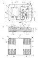
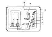
例えば特許文献1に開示されている技術は、図9に示すように、振動子と半導体素子とを垂直方向に配置する構成とし、いわゆるH型構造のパッケージベースを採用した電子デバイスである。この電子デバイス1では、振動片3を実装する中間基板2の裏面側、すなわち半導体素子5を実装する面に、振動片実装用パッド4と、電子デバイス1を実装するための外部端子7とを電気的に接続するパターン(不図示)を形成している。そして、振動子としての振動特性の検査を、外部端子7を介して行うことが可能な構成としている。振動特性の検査調整後には、外部端子7と振動片実装用パッド4を電気的に接続するパターンを切断し、外部端子7を固有の機能を有する端子として独立させることができる。
For example, the technique disclosed in
また、特許文献2に開示されている技術は、図10に示すように、振動子と半導体素子とを水平方向に配置する構成としたものである。なお、図10(A)は電子デバイスの断面構成を示す図であり、図10(B)は電子デバイスの平面構成を示す図である。特許文献2に開示されている電子デバイス1aでは、振動片3aの実装スペースの横に設けられた半導体素子5aの実装スペースに、振動片実装用パッド4aと電気的に接続されたモニター用電極端子8aを形成している。このような配置形態とされるモニター用電極端子8aは、半導体素子5aが実装された後、樹脂9aで被覆されることにより、外部に晒されることが無くなる。
Further, the technique disclosed in
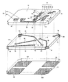
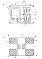
さらに、特許文献3に開示されている技術は、図11に示すような形態をしている。なお、図11(A)は電子デバイスの平面形態を示す図であり、図11(B)は電子デバイスの裏面形態を示す図である。この様な形態を有する電子デバイス1bは、半導体素子の実装スペースに中径パッド6bを形成している。そして、中径パッド6bは、振動片実装用パッド4bと電気的に接続された半導体素子実装用パッド5bと、切断用パターン6b1を介して接続されている。そして、中径パッド6bを設けたベース基板2bの裏面には、外部端子7bの他に、モニター用電極端子8bを形成している。このような形態のパッケージを有する電子デバイス1bでは、振動子を構成した後、モニター用電極端子8bを介して振動子の振動特性の検査調整を行った後、切断用パターン6b1を切断することでモニター用電極端子8bを電気的に切断し、電子デバイス1bを構成する。
Furthermore, the technique disclosed in
上記特許文献に開示されているような技術では、それぞれモニター用電極端子の配置箇所や利用形態に工夫を凝らし、小型化、低背化といったそれぞれの目的に適した構造とされている。しかし、特許文献1に開示されている技術は、本願発明の対象とされる低背化には適さない構造である。また、特許文献2に開示されっている技術は、モニター用電極端子を振動子や半導体素子を実装する側の主面に配置しているため、振動特性を調整する際に、ベース基板の裏面側からモニター用電極端子にプローブを当接させるという事ができない。このため、振動特性の調整を行う際には、端子を備えた専用のホルダが必要となってしまう。
In the techniques disclosed in the above-mentioned patent documents, the arrangement and usage of the monitor electrode terminals are devised, and the structure is suitable for each purpose such as downsizing and low profile. However, the technique disclosed in
特許文献3に開示された技術では、ベース基板の裏面側(他方の主面側)からモニター用電極端子にプローブを当接させることができる構成である。しかし、振動特性の検査、調整を終えた後に切断する切断用パターンの切断が不完全であった場合には、浮遊容量の発生による振動特性の悪化や、実装時の短絡が生ずる虞がある。
In the technique disclosed in
本実施形態では、上記のような問題を解決し、ベース基板に切断用パターンを有する場合に、この切断用パターンの切断状態を確実なものとすることのできる電子デバイスを提供すると共に、この電子デバイスの製造方法を提供することを目的とする。 The present embodiment solves the above problems and provides an electronic device capable of ensuring the cutting state of the cutting pattern when the base substrate has the cutting pattern. An object of the present invention is to provide a device manufacturing method.
本発明は上記課題の少なくとも一部を解決するためになされたものであり、以下の形態または適用例として実現することが可能である。
[適用例1]振動片と半導体素子とを水平方向に並べて実装したベース基板を備える電子デバイスであって、前記ベース基板の一方の主面に、前記振動片を実装するための振動片実装用パッドと、前記振動片実装用パッドと電気的に接続されている第1半導体素子接続用パッドと、前記ベース基板の他方の主面に形成されたモニター用電極端子と電気的に接続されている中継パッドと、前記第1半導体素子接続用パッドと前記中継パッドとを電気的に接続する切断用パターンとを有し、前記切断用パターンは、前記半導体素子を実装した状態において切断されており、前記切断用パターンの切断位置である前記ベース基板の表面に凹陥部を有することを特徴とする電子デバイス。
SUMMARY An advantage of some aspects of the invention is to solve at least a part of the problems described above, and the invention can be implemented as the following forms or application examples.
Application Example 1 An electronic device including a base substrate on which a resonator element and a semiconductor element are mounted in a horizontal direction, and for mounting the resonator element on one main surface of the base substrate A pad, a first semiconductor element connection pad electrically connected to the vibration piece mounting pad, and a monitor electrode terminal formed on the other main surface of the base substrate are electrically connected. A relay pad, and a cutting pattern for electrically connecting the first semiconductor element connection pad and the relay pad, the cutting pattern being cut in a state where the semiconductor element is mounted; An electronic device comprising a recess on a surface of the base substrate, which is a cutting position of the cutting pattern.
このような特徴を有する電子デバイスによれば、切断用パターンの切断状態を確実なものとすることができる。 According to the electronic device having such a feature, the cutting state of the cutting pattern can be ensured.
[適用例2]適用例1に記載の電子デバイスであって、前記中継パッドは、前記半導体素子を実装するための第2半導体素子接続用パッドであり、前記モニター用電極端子は、前記ベース基板の他方の面に形成された実装端子であることを特徴とする電子デバイス。 Application Example 2 In the electronic device according to Application Example 1, the relay pad is a second semiconductor element connection pad for mounting the semiconductor element, and the monitor electrode terminal is the base substrate An electronic device, characterized in that the electronic device is a mounting terminal formed on the other surface.
実装端子(外部実装端子)を、いわゆるモニター用電極端子として利用することとなるため、パッケージが小型化された場合であっても、確実にプローブ当接面を確保することが可能となる。 Since the mounting terminals (external mounting terminals) are used as so-called monitoring electrode terminals, the probe contact surface can be reliably secured even when the package is downsized.
[適用例3]一方の面に、振動片を実装するための振動片実装用パッドと、前記振動片実装用パッドと電気的に接続されている第1半導体素子接続用パッドと、他方の面に形成されたモニター用電極端子と電気的に接続されている中継パッドと、前記第1半導体素子接続用パッドと前記中継パッドとを電気的に接続する切断用パターンを有し、前記振動片と半導体素子とを水平方向に並べて実装可能とするベース基板を備える電子デバイスの製造方法であって、前記振動片実装用パッドに対して振動片を実装する振動片実装工程と、前記モニター用電極端子を介して前記振動片の発振と共振周波数の調整を行う周波数調整工程と、前記周波数調整工程後、前記切断用パターンを切断し、前記ベース基板の表面に凹陥部を形成するパターン切断工程とを有することを特徴とする電子デバイスの製造方法。 Application Example 3 On one surface, a resonator element mounting pad for mounting a resonator element, a first semiconductor element connection pad electrically connected to the resonator element mounting pad, and the other surface A relay pad that is electrically connected to the monitor electrode terminal formed on the substrate, a cutting pattern that electrically connects the first semiconductor element connection pad and the relay pad, A method of manufacturing an electronic device including a base substrate that can be mounted by arranging semiconductor elements in a horizontal direction, the resonator element mounting step for mounting the resonator element on the resonator element mounting pad, and the monitor electrode terminal A frequency adjusting step of adjusting the oscillation of the resonator element and the resonance frequency via the step, and a pattern cutting for cutting the cutting pattern after the frequency adjusting step and forming a concave portion on the surface of the base substrate Method for fabricating an electronic device and having a degree.
このような特徴を有する電子デバイスの製造方法により電子デバイスを製造すれば、切断用パターンの切断状態を確実なものとすることができる。 If an electronic device is manufactured by the manufacturing method of an electronic device having such characteristics, the cutting state of the cutting pattern can be ensured.
以下、本発明の電子デバイス、および電子デバイスの製造方法についての実施の形態を、図面を参照しつつ詳細に説明する。図1(A)は、電子デバイスの平面構造を示す図であり、図1(B)は、同図(A)におけるA−A断面を示す図であり、図1(C)は、電子デバイスの裏面構造を示す図である。 Hereinafter, embodiments of an electronic device and a method for manufacturing the electronic device of the present invention will be described in detail with reference to the drawings. 1A is a diagram illustrating a planar structure of an electronic device, FIG. 1B is a diagram illustrating a cross section taken along the line AA in FIG. 1A, and FIG. 1C is an electronic device. It is a figure which shows the back surface structure of.
本実施形態に係る電子デバイス10は、振動片110と、半導体素子としてのICチップ114、およびパッケージ11を基本として構成される。
振動片110は、ATカット水晶振動片などの水晶振動片を用いることができる。なお振動片110は、この他にも、水晶素板のカット角や主振動の形態に違いを有する音叉型水晶振動片や、弾性表面波水晶振動片などでもよい。また振動片の材料としては水晶以外にもタンタル酸リチウム、ニオブ酸リチウムなどを用いてもよい。さらに水晶振動片の代わりに圧電振動片以外の各種振動片を用いることも可能であり、例えばシリコン基板を加工して形成されたMEMS(Micro Electro Mechanical Systems)振動片等を用いた場合であっても、本実施形態に係る電子デバイス10を構成することができる。
The
As the
ICチップ114としては、振動子(振動片110として圧電素板を実装した場合には圧電振動子)を発振させる回路構造を有する半導体素子から構成された集積回路等を採用することができる。ICチップ114には複数の電極パッド(不図示)が設けられている。
As the
パッケージ11は、ベース基板12と、このベース基板12に実装した振動片110を封止して振動子を構成するための蓋体112を基本として構成される。本実施形態に係るベース基板12は、第1の基板14、第2の基板16、および第3の基板18を積層させて構成される。各基板の構成材料としては、アルミナセラミックスやガラスセラミックス等のセラミックス材料から成り、グリーンシート法により積層焼結されて一体化される。第2の基板16、および第3の基板18には、金属パターンが形成されている。このため図2には、第2の基板16と第3の基板18に形成された金属パターンの構成が明確となるように、第2の基板16、および第3の基板18の分解斜視図を示すこととする。
The
第1の基板14は、ベース基板12を構成する基板の最上層であり、振動片110とICチップ114の外周を囲む第1の凹部20、および第2の凹部22を形成する枠体である。第1の凹部20は、内部に振動片110を収容する内部空間を形成する。第2の凹部22は、内部にICチップ114を収容する空間を形成している。なお第1の基板14の厚みは、少なくとも振動片110の厚みよりも厚く形成している。第1の凹部20に振動片110を収容した後に、詳細を後述する蓋体112により、第1の凹部20を封止することを可能とするためである。
The
第2の基板16は、ベース基板12を構成する基板の中間層であり、上述した第1の基板14との接合面である第1の主面には、金属パターンと、第1の主面に形成された金属パターンを第1の主面の裏面側である第2の主面に落とし込むビアホールを有する。第1の主面に形成された金属パターンには、振動片110を実装するための振動片実装用パッド24やICチップ114を実装するためのICチップ実装パッド30、およびこれらの金属パターンとビアホールを電気的に接続する接続パターン56,58,60,61,62,64が存在する。本実施形態に係る第2の基板16には、振動片実装用パッド24として、第1振動片実装用パッド26と、第2振動片実装用パッド28が存在する。また、ICチップ実装パッド30としては、GNDパッド32、foutパッド34、振動片接続用第1パッド36(第1半導体素子接続用パッド)、振動片接続用第2パッド38(第1半導体素子接続用パッド)、Vcパッド40(第2半導体素子接続用パッド)、およびVddパッド42(第2半導体素子接続用パッド)などを有する。
The
また、ビアホールとしては、第1のビアホール44から第6のビアホール54を有する。ビアホールのうち、第1のビアホール44は、第1振動片実装用パッド26の直下に設けられている。また、第2のビアホール46は、GNDパッド32と振動片接続用第1パッド36との間に設けられ、GNDパッド32と接続パターン58により接続されている。また、第3のビアホール48は、foutパッド34と、このfoutパッド34に最寄の角部との間に設けられ、接続パターン60によりfoutパッド34と接続されている。また、第4のビアホール50は、振動片接続用第1パッド36から振動片実装位置側へ延設された接続パターン61の先端位置に設けられている。また、第5のビアホール52は、Vcパッド40を基点として、振動片接続用第1パッド36と点対称となる位置に設けられ、接続パターン62によりVcパッド40と接続されている。さらに第6のビアホール54は、Vddパッド42を基点として振動片接続用第2パッド38と点対称となる位置に設けられ、接続パターン64によりVddパッド42と接続されている。
In addition, as the via holes, the first via
また、本実施形態に係る電子デバイス10のパッケージ11を構成する第2基板16では、振動片接続用第1パッド36とVcパッド40、および振動片接続用第2パッド38とVddパッド42とをそれぞれ電気的に接続する切断用パターン66,68を有する。
Further, in the
第3の基板18は、ベース基板12を構成する基板の最下層であり、第2の基板16と接合する第1の主面と、パッケージの外部に晒されることとなる第2の主面とを有する。また、第3の基板18の四隅には切欠きが形成され、第1〜第4のキャスタレーション82〜88が形成されている。第3の基板18における第1の主面には、第2の基板16におけるビアホールの落とし込み位置に対応したビアホール対応パッドと、接続パターンが形成されている。ビアホール対応パッドには、第1のビアホール対応パッド70〜第6のビアホール対応パッド80が存在し、それぞれ第1のビアホール44〜第6のビアホール54の対応位置に配置形成される。
The
第1のビアホール対応パッド70と、第4のビアホール対応パッド76とは、接続パターン90により接続されている。これにより、第1振動片実装用パッド26と、振動片接続用第1パッド36とが電気的に接続されることとなる。また、第2のビアホール対応パッド72は、接続パターン92を介して第3のキャスタレーション86と接続されている。また、第3のビアホール対応パッド74は、接続パターン94を介して第2のキャスタレーション84と接続されている。また、第5のビアホール対応パッド78は、接続パターン96を介して第4のキャスタレーション88と接続されている。さらに、第6のビアホール対応パッド80は、接続パターン98を介して第1のキャスタレーション82と接続されている。
The first via
第3の基板18における第2の主面には、4つの外部実装用端子が形成されている。4つの外部実装用端子はそれぞれ、第3の基板18の四隅に形成された第1〜第4のキャスタレーション82〜88のいずれか1つに接続されており、キャスタレーションおよび接続電極を介して電気的に接続されたパッド(GNDパッド32、foutパッド34、Vcパッド40、Vddパッド42)の属性によりそれぞれ、GND端子104、fout端子102、Vc端子106、Vdd端子100を構成する。
Four external mounting terminals are formed on the second main surface of the
蓋体112は、第1の基板14における第1の凹部20の上部開口部を覆う部材である。蓋体112は、平板状又は第1の凹部20の外周に沿ってキャップ状、即ち第1の凹部20を凸状に覆う形状とすることができる。本実施形態では、蓋体112の一例として、板状の金属リッドを採用することとする。なお、蓋体112と第1の基板14との接合には、図示しないシームリングなどの金属ロウ材や、低融点ガラスなどのロウ材などを用いることができる。
The
このような構成とした本実施形態に係るパッケージ11では、切断用パターン66,68が切断されていない状態においては、Vc端子106と第1振動片実装用パッド26、Vdd端子100と第2振動片実装用パッド28がそれぞれ電気的に接続されることとなり、Vc端子106とVdd端子100とが、モニター用電極端子としての役割を担うこととなる。一方、切断用パターン66,68が切断された後には、振動片接続用第1パッド36とVcパッド40、振動片接続用第2パッド38とVddパッド42が、それぞれ電気的に分離されるため、Vc端子106とVdd端子100とは、それぞれ固有の役割を担う端子となり、パッケージ11の外部(外部実装用端子形成面側)から直接、振動片110の振動特性を検出することは出来なくなる。
In the
振動片110は、第1振動片実装用パッド26、および第2振動片実装用パッド28に対し、導電性接着剤等を介して実装される。これにより、振動片接続用第1パッド36と、振動片接続用第2パッド38とが、振動片110における図示しない励振電極と電気的に接続されることとなる。ここで、振動片110を弾性表面波水晶振動片などとした場合には、導電性接着剤を介した実装の替わりに、ワイヤボンディングなどの手法を採るようにすれば良い。
The
ICチップ114は、第2の凹部22に設けられたICチップ実装パッド30(GNDパッド32、foutパッド34、振動片接続用第1パッド36、振動片接続用第2パッド38、Vcパッド40、およびVddパッド42)に対して、金属バンプなどを介したフリップチップボンディングにより実装される。これにより、振動片接続用第1パッド36と振動片接続用第2パッド38と、foutパッド34とVddパッド42とは、ICチップ114を介して接続されることとなり、振動片110は、ICチップ114に記録された動作条件に基づいて発振することとなる。
The
ICチップ114の外周であって、ICチップ114を実装した第2の凹部22の内部領域には、樹脂部材116が充填される。樹脂部材116の充填により、ICチップ114の実装面に水分が付着することによる振動特性の劣化や、塵埃が付着することによる短絡等を防止することができる。このため、樹脂部材116は絶縁性とし、一例としては、一般的なモールド樹脂を採用することができる。
A
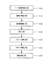
次に、上記のような構成の電子デバイスの製造方法について図3を参照して説明する。
まず、ベース基板12は、各基板形状に形成された第1の基板14、第2の基板16、および第3の基板18のうち、第2の基板16と第3の基板18に対して、金属パターンの形成を行う。金属パターンの形成は、スクリーン印刷などの手法により行われ、金属パターンは、タングステンやモリブデン等を下地層とし、第2、第3の基板16,18は、第1の基板14と共に焼成されることにより一体化される(ベース基板製造工程:S100)。そして焼成後に、金属パターンに対してメッキ処理を施し、ニッケル層、および金層を形成する。
Next, a method for manufacturing the electronic device having the above configuration will be described with reference to FIG.
First, of the
形成されたベース基板12の第1の凹部20に設けられた第1振動片実装用パッド26と第2振動片実装用パッド28に対し、導電性接着剤の塗布を行う。導電性接着剤が塗布された第1振動片実装用パッド26と第2振動片実装用パッド28に対して振動片110を搭載し、振動片110の実装を行う(振動片実装工程:S110)。
A conductive adhesive is applied to the first vibration
振動片110を実装したベース基板12を図4に示すようなホルダ150にセットする。ホルダ150には、底面に開口部152を有する凹部154が形成されており、ベース基板12は、この開口部152から振動片110の励振電極(不図示)が覗くこととなるように、ホルダ150に対してセットされる。このようにセットされたベース基板12のVc端子106とVdd端子100に対して、ネットワークアナライザ等の特性試験装置160のプローブ162を当接させる。ここで、特性試験装置160としては、ベース基板12に実装された振動片110の共振周波数やCI(クリスタルインピーダンス)値、インダクタンス、容量等の等価パラメータを測定することができるものであれば良い。
The
Vc端子106とVdd端子100に対して特性試験装置160のプローブ162を当接させ、振動片110の共振周波数等の特性を検出すると共に、ホルダ150の開口部152を介して振動片110の励振電極に対してレーザーを照射し、共振周波数の調整を行う(周波数調整工程:S120)。
The
周波数調整工程終了後、第1の凹部20における上部開口部を蓋体112で封止する。蓋体112の接合は、図示しないシームリングを用いたシーム溶接や、金属系ロウ材を用いた液相拡散接合法などを採用することができる。第1の凹部20を蓋体112により封止することにより、振動子が構成される。詳細を後述するパターン切断工程の前に第1の凹部20を封止することにより、切断用パターン66,68の切断によって生じた塵埃が振動片110に付着して、振動特性を劣化させることを防止することができる(封止工程:S130)。
After the frequency adjustment step, the upper opening in the
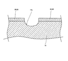
周波数調整工程を終えた後、振動片110を実装したベース基板12をホルダ150から取り外し、切断用パターン66,68の切断を行う。切断用パターン66,68の切断は、Nd−YAGレーザーやNd−YVO4レーザーなどのレーザーを照射することにより行うことができる。レーザーにより切断された切断用パターン66,68の切断痕16aは、図5に示すように、ベース基板12における第2の基板16の一方の主面、すなわち表面をえぐるように凹陥させた形態となる。
After the frequency adjustment process is finished, the
レーザーの照射は、1回であっても、複数回であっても良い。レーザーを複数回照射する場合、照射位置を切断用パターン66,68の配線方向に沿ってずらす事で、切断部の幅を広げる事ができる。なお、レーザーの照射を複数回行う場合には、レーザーの照射により生ずる塵埃を吸引除去しながら行うようにすることが望ましい。レーザーにより切断された切断痕16aが残る箇所に、複数回目のレーザー照射によって生じた金属パターンを含む塵埃が付着し、切断用パターン66,68の電気的な切断が妨げられる可能性が生ずるからである(パターン切断工程:S140)。
Laser irradiation may be performed once or a plurality of times. When the laser is irradiated a plurality of times, the width of the cut portion can be increased by shifting the irradiation position along the wiring direction of the cutting
パターン切断工程の後、第2の凹部22に対してICチップ114を実装する。ICチップ114は、金バンプなどを介したフリップチップボンディングにより実装する(ICチップ実装工程:S150)。ICチップ114を実装した後、第2の凹部22の隙間部分に、樹脂部材116を充填し、固化させる(樹脂充填工程:S160)。
After the pattern cutting step, the
このようにして形成される電子デバイス10によれば、振動片110とICチップ114を水平方向に配置した、低背化に適した構成であると言える。また、振動片110の振動特性の検査、調整時においては、外部実装端子をモニター用電極端子として利用することにより、小型化された場合であっても確実に、プローブ162を当接させる面積を確保することができる。さらに、外部実装端子をモニター用電極端子として利用するため、振動片110を実装したベース基板12をホルダ150にセットした状態で裏面側から、プローブ162をモニター用電極端子に当接させることが可能となる。このため、振動特性等を検出しながら、共振周波数の調整を行うことができる。
According to the
上記実施形態では、切断用パターン66,68のパターン幅も、他の金属パターンのパターン幅と等しいように図に示した。しかしながら、図6に示すように、切断用パターン66,68のパターン幅を、他の金属パターンのパターン幅に比べて狭くするようにしても良い。このような構成とすることにより、切断用パターン66,68の切断が容易となり、切断の確実性を向上させることができる。
In the above embodiment, the pattern widths of the cutting
また、上記実施形態に係る電子デバイスでは、図7に示すように、切断用パターン66(または切断用パターン68)をGNDパッド32に接続するようにしても良い。このような構成とした場合、GNDパッド32が第2半導体素子接続用パッドとしての役割を担い、周波数調整工程においては、GND端子104とVdd端子100が、モニター用電極端子としての役割を担うこととなる。このように、本実施形態に係るパッケージ11では、外部実装端子をモニター用電極端子として利用する構成としたことにより、切断用パターン66,68の接続先の組み合わせを変える事ができ、金属パターンの設計的な規制を緩和することができる。
In the electronic device according to the above embodiment, the cutting pattern 66 (or the cutting pattern 68) may be connected to the
また、上記実施形態に係る電子デバイスは、外部実装端子がモニター用電極端子の役割を担う構成としていた。しかしながら、外部実装端子とモニター用電極端子とを別体として設けた、図8に示すような形態の電子デバイスであっても、本発明の一部とみなすことができる。なお、図8において、図8(A)は電子デバイスの平面構成を示す図であり、図8(B)は電子デバイスの裏面側構成を示す図である。 In the electronic device according to the above embodiment, the external mounting terminal serves as a monitoring electrode terminal. However, even an electronic device having a form as shown in FIG. 8 in which the external mounting terminal and the monitor electrode terminal are provided separately can be regarded as a part of the present invention. 8A is a diagram illustrating a planar configuration of the electronic device, and FIG. 8B is a diagram illustrating a rear surface side configuration of the electronic device.
図8に示す電子デバイス10aは、その基本的構成は、上述した実施形態に係る電子デバイス10と同様である。相違点としてはベース基板の構成において、ICチップ114と電気的に接続されることが無い中径パッド37,39を設けた点にある。そして、中径パッド37,39は、第3の基板18の第2の主面に形成したモニター用電極端子と電気的に接続されている。
The basic configuration of the
さらに、振動片接続用第1パッド36と中径パッド37との間には、切断用パターン66が設けられ、振動片接続用第2パッド38と中径パッド39との間には、切断用パターン68が設けられている。このような構成とされるベース基板12を有する電子デバイス10aでは、上述した周波数調整工程終了後、ベース基板12の表面をえぐるような凹陥部を形成するように、切断用パターン66,68を切断し、ICチップ114を実装する。このような構成の電子デバイスであっても、切断用パターン66,68を切断する際、凹陥状となる切断痕を形成することで、切断用パターン66,68の切断を確実なものとすることができる。
Further, a cutting
なお、図1、図6、図7に示す電子デバイス10、および図8に示す電子デバイス10aは、説明を理解し易くするために、切断用パターン66,68が切断されていない状態を示しているが、実際に構成される電子デバイス10,10aでは、切断用パターン66,68は、切断状態とされる。
The
10………電子デバイス、11………パッケージ、12………ベース基板、14………第1の基板、16………第2の基板、18………第3の基板、20………第1の凹部、22………第2の凹部、24………振動片実装用パッド、26………第1振動片実装用パッド、28………第2振動片実装用パッド、30………ICチップ実装パッド、32………GNDパッド、34………foutパッド、36………振動片接続用第1パッド、38………振動片接続用第2パッド、40………Vcパッド、42………Vddパッド、44………第1ビアホール、46………第2ビアホール、48………第3ビアホール、50………第4ビアホール、52………第5ビアホール、54………第6ビアホール、56,58,60,61,62,64………接続パターン、66,68………切断用パターン、70………第1ビアホール対応パッド、72………第2ビアホール対応パッド、74………第3ビアホール対応パッド、76………第4ビアホール対応パッド、78………第5ビアホール対応パッド、80………第6ビアホール対応パッド、82………第1のキャスタレーション、84………第2のキャスタレーション、86………第3のキャスタレーション、88………第4のキャスタレーション、90,92,94,96,98………接続パターン、100………Vdd端子、102………fout端子、104………GND端子、106………Vc端子。
10 …………
Claims (3)
前記ベース基板の一方の主面に、
前記振動片を実装するための振動片実装用パッドと、
前記振動片実装用パッドと電気的に接続されている第1半導体素子接続用パッドと、
前記ベース基板の他方の主面に形成されたモニター用電極端子と電気的に接続されている中継パッドと、
前記第1半導体素子接続用パッドと前記中継パッドとを電気的に接続する切断用パターンと
を有し、
前記切断用パターンは、前記半導体素子を実装した状態において切断されており、前記切断用パターンの切断位置である前記ベース基板の表面に凹陥部を有することを特徴とする電子デバイス。 An electronic device including a base substrate on which a resonator element and a semiconductor element are mounted in a horizontal direction,
On one main surface of the base substrate,
A vibration piece mounting pad for mounting the vibration piece;
A first semiconductor element connection pad electrically connected to the resonator element mounting pad;
A relay pad electrically connected to the monitor electrode terminal formed on the other main surface of the base substrate;
A cutting pattern for electrically connecting the first semiconductor element connection pad and the relay pad;
The electronic device is characterized in that the cutting pattern is cut in a state where the semiconductor element is mounted, and has a recessed portion on the surface of the base substrate, which is a cutting position of the cutting pattern.
前記中継パッドは、前記半導体素子を実装するための第2半導体素子接続用パッドであり、前記モニター用電極端子は、前記ベース基板の他方の面に形成された実装端子であることを特徴とする電子デバイス。 The electronic device according to claim 1,
The relay pad is a second semiconductor element connection pad for mounting the semiconductor element, and the monitor electrode terminal is a mounting terminal formed on the other surface of the base substrate. Electronic devices.
前記振動片実装用パッドに対して振動片を実装する振動片実装工程と、
前記モニター用電極端子を介して前記振動片の発振と共振周波数の調整を行う周波数調整工程と、
前記周波数調整工程後、前記切断用パターンを切断し、前記ベース基板の表面に凹陥部を形成するパターン切断工程とを有することを特徴とする電子デバイスの製造方法。 A vibration piece mounting pad for mounting the vibration piece on one surface, a first semiconductor element connection pad electrically connected to the vibration piece mounting pad, and a monitor formed on the other surface A relay pad that is electrically connected to the electrode terminal, a cutting pattern that electrically connects the first semiconductor element connection pad and the relay pad, and the resonator element and the semiconductor element are horizontally A method of manufacturing an electronic device comprising a base substrate that can be mounted side by side in a direction,
A resonator element mounting step of mounting a resonator element on the resonator element mounting pad;
A frequency adjustment step of adjusting the oscillation and resonance frequency of the resonator element via the monitor electrode terminal;
A pattern cutting step of cutting the cutting pattern after the frequency adjusting step to form a recessed portion on the surface of the base substrate.
Priority Applications (3)
| Application Number | Priority Date | Filing Date | Title |
|---|---|---|---|
| JP2010063876A JP2011199579A (en) | 2010-03-19 | 2010-03-19 | Electronic device and method for manufacturing electronic device |
| US13/044,829 US20110228501A1 (en) | 2010-03-19 | 2011-03-10 | Electronic device, and method of manufacturing electronic device |
| CN2011100684981A CN102201794A (en) | 2010-03-19 | 2011-03-18 | Electronic device and method of manufacturing electronic device |
Applications Claiming Priority (1)
| Application Number | Priority Date | Filing Date | Title |
|---|---|---|---|
| JP2010063876A JP2011199579A (en) | 2010-03-19 | 2010-03-19 | Electronic device and method for manufacturing electronic device |
Publications (2)
| Publication Number | Publication Date |
|---|---|
| JP2011199579A true JP2011199579A (en) | 2011-10-06 |
| JP2011199579A5 JP2011199579A5 (en) | 2013-04-11 |
Family
ID=44647113
Family Applications (1)
| Application Number | Title | Priority Date | Filing Date |
|---|---|---|---|
| JP2010063876A Withdrawn JP2011199579A (en) | 2010-03-19 | 2010-03-19 | Electronic device and method for manufacturing electronic device |
Country Status (3)
| Country | Link |
|---|---|
| US (1) | US20110228501A1 (en) |
| JP (1) | JP2011199579A (en) |
| CN (1) | CN102201794A (en) |
Cited By (4)
| Publication number | Priority date | Publication date | Assignee | Title |
|---|---|---|---|---|
| JP2014093571A (en) * | 2012-10-31 | 2014-05-19 | Kyocera Crystal Device Corp | Piezoelectric device |
| JP2016086325A (en) * | 2014-10-28 | 2016-05-19 | 京セラクリスタルデバイス株式会社 | Piezoelectric device |
| JP2018060835A (en) * | 2016-09-30 | 2018-04-12 | 日亜化学工業株式会社 | Semiconductor device package and semiconductor device using the same |
| JP2020167504A (en) * | 2019-03-29 | 2020-10-08 | 株式会社大真空 | Piezoelectric vibration device |
Families Citing this family (2)
| Publication number | Priority date | Publication date | Assignee | Title |
|---|---|---|---|---|
| JP6561487B2 (en) * | 2015-02-16 | 2019-08-21 | セイコーエプソン株式会社 | Oscillator circuit, oscillator, electronic device and mobile object |
| CN113422587A (en) * | 2021-05-13 | 2021-09-21 | 北京七芯中创科技有限公司 | Cylindrical crystal oscillator and chip single packaging structure based on multilayer concave embedded substrate |
Citations (8)
| Publication number | Priority date | Publication date | Assignee | Title |
|---|---|---|---|---|
| JPH04348058A (en) * | 1991-05-24 | 1992-12-03 | Fujitsu Ltd | Organic substrate containing glass fiber |
| JP2000332386A (en) * | 1999-05-17 | 2000-11-30 | U Corporation | Method of forming circuit pattern |
| JP2001076569A (en) * | 1999-09-07 | 2001-03-23 | Fujikura Ltd | Method for manufacturing membrane circuit |
| JP2002190710A (en) * | 2000-12-20 | 2002-07-05 | Nippon Dempa Kogyo Co Ltd | Crystal oscillator for surface mounting |
| JP2004328505A (en) * | 2003-04-25 | 2004-11-18 | Toyo Commun Equip Co Ltd | Piezoelectric oscillator |
| JP2005223640A (en) * | 2004-02-05 | 2005-08-18 | Toyo Commun Equip Co Ltd | Package, surface mounted piezoelectric oscillator using the same, and frequency adjusting method therefor |
| JP2008278227A (en) * | 2007-04-27 | 2008-11-13 | Kyocera Kinseki Corp | Manufacturing method of piezoelectric oscillator |
| JP2008301196A (en) * | 2007-05-31 | 2008-12-11 | Kyocera Kinseki Corp | Piezoelectric oscillator |
Family Cites Families (5)
| Publication number | Priority date | Publication date | Assignee | Title |
|---|---|---|---|---|
| JP2002124828A (en) * | 2000-10-12 | 2002-04-26 | Sharp Corp | Oscillator and method for adjusting oscillation characteristic thereof |
| US6640435B2 (en) * | 2001-02-20 | 2003-11-04 | Power Integrations, Inc. | Methods for trimming electrical parameters in an electrical circuit |
| JP2002335128A (en) * | 2001-05-09 | 2002-11-22 | Seiko Epson Corp | Piezoelectric device |
| US7266869B2 (en) * | 2003-07-30 | 2007-09-11 | Kyocera Corporation | Method for manufacturing a piezoelectric oscillator |
| JP5087335B2 (en) * | 2007-07-19 | 2012-12-05 | 日本電波工業株式会社 | Crystal oscillator for surface mounting |
-
2010
- 2010-03-19 JP JP2010063876A patent/JP2011199579A/en not_active Withdrawn
-
2011
- 2011-03-10 US US13/044,829 patent/US20110228501A1/en not_active Abandoned
- 2011-03-18 CN CN2011100684981A patent/CN102201794A/en active Pending
Patent Citations (8)
| Publication number | Priority date | Publication date | Assignee | Title |
|---|---|---|---|---|
| JPH04348058A (en) * | 1991-05-24 | 1992-12-03 | Fujitsu Ltd | Organic substrate containing glass fiber |
| JP2000332386A (en) * | 1999-05-17 | 2000-11-30 | U Corporation | Method of forming circuit pattern |
| JP2001076569A (en) * | 1999-09-07 | 2001-03-23 | Fujikura Ltd | Method for manufacturing membrane circuit |
| JP2002190710A (en) * | 2000-12-20 | 2002-07-05 | Nippon Dempa Kogyo Co Ltd | Crystal oscillator for surface mounting |
| JP2004328505A (en) * | 2003-04-25 | 2004-11-18 | Toyo Commun Equip Co Ltd | Piezoelectric oscillator |
| JP2005223640A (en) * | 2004-02-05 | 2005-08-18 | Toyo Commun Equip Co Ltd | Package, surface mounted piezoelectric oscillator using the same, and frequency adjusting method therefor |
| JP2008278227A (en) * | 2007-04-27 | 2008-11-13 | Kyocera Kinseki Corp | Manufacturing method of piezoelectric oscillator |
| JP2008301196A (en) * | 2007-05-31 | 2008-12-11 | Kyocera Kinseki Corp | Piezoelectric oscillator |
Cited By (5)
| Publication number | Priority date | Publication date | Assignee | Title |
|---|---|---|---|---|
| JP2014093571A (en) * | 2012-10-31 | 2014-05-19 | Kyocera Crystal Device Corp | Piezoelectric device |
| JP2016086325A (en) * | 2014-10-28 | 2016-05-19 | 京セラクリスタルデバイス株式会社 | Piezoelectric device |
| JP2018060835A (en) * | 2016-09-30 | 2018-04-12 | 日亜化学工業株式会社 | Semiconductor device package and semiconductor device using the same |
| JP2020167504A (en) * | 2019-03-29 | 2020-10-08 | 株式会社大真空 | Piezoelectric vibration device |
| WO2020202814A1 (en) * | 2019-03-29 | 2020-10-08 | 株式会社大真空 | Piezoelectric vibrating device |
Also Published As
| Publication number | Publication date |
|---|---|
| US20110228501A1 (en) | 2011-09-22 |
| CN102201794A (en) | 2011-09-28 |
Similar Documents
| Publication | Publication Date | Title |
|---|---|---|
| JP6020663B2 (en) | Oscillator | |
| US8710718B2 (en) | Sealing member for piezoelectric resonator device, and piezoelectric resonator device | |
| JP2011199579A (en) | Electronic device and method for manufacturing electronic device | |
| JP2011199577A (en) | Package, electronic device, and method for manufacturing electronic device | |
| JP2013058864A (en) | Piezoelectric device | |
| JP2008301196A (en) | Piezoelectric oscillator | |
| JP2009010864A (en) | Body casing member for piezoelectric vibration device, piezoelectric vibration device, and method of manufacturing piezoelectric vibration device | |
| JP2010035078A (en) | Piezoelectric oscillator | |
| JP4501875B2 (en) | Piezoelectric vibration device and manufacturing method thereof | |
| JP5098668B2 (en) | Surface mount type piezoelectric oscillator | |
| JP2004214799A (en) | Piezoelectric oscillator and method of measuring piezoelectric oscillator | |
| JP5171148B2 (en) | Piezoelectric oscillator | |
| JP2010035077A (en) | Piezoelectric oscillator | |
| JP2009232336A (en) | Piezoelectric oscillator | |
| JP2009055354A (en) | Package for piezoelectric vibration device and piezoelectric vibration device | |
| JP4167557B2 (en) | Method for manufacturing piezoelectric oscillator | |
| JP2003318653A (en) | Piezoelectric vibrating device | |
| JP5942312B2 (en) | Assembling method of crystal oscillator | |
| JP6604071B2 (en) | Piezoelectric vibration device | |
| JP4578231B2 (en) | Piezoelectric oscillator and manufacturing method thereof | |
| JP6569267B2 (en) | Piezoelectric oscillator | |
| JP4472445B2 (en) | Method for manufacturing piezoelectric oscillator | |
| JP5521732B2 (en) | Package Base and Oscillator Manufacturing Method | |
| JP7044005B2 (en) | Piezoelectric vibration device | |
| JP5210077B2 (en) | Piezoelectric oscillator |
Legal Events
| Date | Code | Title | Description |
|---|---|---|---|
| A521 | Written amendment |
Free format text: JAPANESE INTERMEDIATE CODE: A523 Effective date: 20130226 |
|
| A621 | Written request for application examination |
Free format text: JAPANESE INTERMEDIATE CODE: A621 Effective date: 20130226 |
|
| A977 | Report on retrieval |
Free format text: JAPANESE INTERMEDIATE CODE: A971007 Effective date: 20131030 |
|
| A131 | Notification of reasons for refusal |
Free format text: JAPANESE INTERMEDIATE CODE: A131 Effective date: 20131119 |
|
| A761 | Written withdrawal of application |
Free format text: JAPANESE INTERMEDIATE CODE: A761 Effective date: 20140115 |