JP2010096739A - 検査装置およびその検査方法 - Google Patents
検査装置およびその検査方法 Download PDFInfo
- Publication number
- JP2010096739A JP2010096739A JP2009056991A JP2009056991A JP2010096739A JP 2010096739 A JP2010096739 A JP 2010096739A JP 2009056991 A JP2009056991 A JP 2009056991A JP 2009056991 A JP2009056991 A JP 2009056991A JP 2010096739 A JP2010096739 A JP 2010096739A
- Authority
- JP
- Japan
- Prior art keywords
- detection signal
- printed circuit
- predetermined
- sensor
- electronic element
- Prior art date
- Legal status (The legal status is an assumption and is not a legal conclusion. Google has not performed a legal analysis and makes no representation as to the accuracy of the status listed.)
- Granted
Links
- 238000007689 inspection Methods 0.000 title claims abstract description 97
- 238000000034 method Methods 0.000 title claims description 41
- 238000001514 detection method Methods 0.000 claims abstract description 113
- 239000000523 sample Substances 0.000 claims description 29
- WABPQHHGFIMREM-UHFFFAOYSA-N lead(0) Chemical compound [Pb] WABPQHHGFIMREM-UHFFFAOYSA-N 0.000 claims description 16
- 238000005070 sampling Methods 0.000 claims description 11
- 238000004364 calculation method Methods 0.000 claims description 4
- 238000012544 monitoring process Methods 0.000 claims description 4
- 230000003213 activating effect Effects 0.000 claims 1
- 230000003287 optical effect Effects 0.000 abstract description 3
- 238000011179 visual inspection Methods 0.000 abstract description 3
- 230000002093 peripheral effect Effects 0.000 description 16
- 238000012360 testing method Methods 0.000 description 10
- 238000002474 experimental method Methods 0.000 description 7
- 230000002159 abnormal effect Effects 0.000 description 6
- 230000008878 coupling Effects 0.000 description 6
- 238000010168 coupling process Methods 0.000 description 6
- 238000005859 coupling reaction Methods 0.000 description 6
- 238000004458 analytical method Methods 0.000 description 4
- 238000010586 diagram Methods 0.000 description 4
- 230000003071 parasitic effect Effects 0.000 description 4
- 238000012795 verification Methods 0.000 description 4
- 239000002131 composite material Substances 0.000 description 3
- 239000000758 substrate Substances 0.000 description 3
- 239000003990 capacitor Substances 0.000 description 2
- 238000004519 manufacturing process Methods 0.000 description 2
- RYGMFSIKBFXOCR-UHFFFAOYSA-N Copper Chemical compound [Cu] RYGMFSIKBFXOCR-UHFFFAOYSA-N 0.000 description 1
- 239000011889 copper foil Substances 0.000 description 1
- 238000005530 etching Methods 0.000 description 1
- 238000010998 test method Methods 0.000 description 1
Images


Classifications
-
- G—PHYSICS
- G01—MEASURING; TESTING
- G01R—MEASURING ELECTRIC VARIABLES; MEASURING MAGNETIC VARIABLES
- G01R31/00—Arrangements for testing electric properties; Arrangements for locating electric faults; Arrangements for electrical testing characterised by what is being tested not provided for elsewhere
- G01R31/28—Testing of electronic circuits, e.g. by signal tracer
- G01R31/302—Contactless testing
- G01R31/312—Contactless testing by capacitive methods
-
- G—PHYSICS
- G01—MEASURING; TESTING
- G01R—MEASURING ELECTRIC VARIABLES; MEASURING MAGNETIC VARIABLES
- G01R31/00—Arrangements for testing electric properties; Arrangements for locating electric faults; Arrangements for electrical testing characterised by what is being tested not provided for elsewhere
- G01R31/28—Testing of electronic circuits, e.g. by signal tracer
- G01R31/2801—Testing of printed circuits, backplanes, motherboards, hybrid circuits or carriers for multichip packages [MCP]
- G01R31/2806—Apparatus therefor, e.g. test stations, drivers, analysers, conveyors
-
- G—PHYSICS
- G01—MEASURING; TESTING
- G01R—MEASURING ELECTRIC VARIABLES; MEASURING MAGNETIC VARIABLES
- G01R31/00—Arrangements for testing electric properties; Arrangements for locating electric faults; Arrangements for electrical testing characterised by what is being tested not provided for elsewhere
- G01R31/28—Testing of electronic circuits, e.g. by signal tracer
- G01R31/302—Contactless testing
- G01R31/304—Contactless testing of printed or hybrid circuits
-
- G—PHYSICS
- G01—MEASURING; TESTING
- G01R—MEASURING ELECTRIC VARIABLES; MEASURING MAGNETIC VARIABLES
- G01R31/00—Arrangements for testing electric properties; Arrangements for locating electric faults; Arrangements for electrical testing characterised by what is being tested not provided for elsewhere
- G01R31/28—Testing of electronic circuits, e.g. by signal tracer
- G01R31/302—Contactless testing
- G01R31/315—Contactless testing by inductive methods
Landscapes
- Engineering & Computer Science (AREA)
- General Engineering & Computer Science (AREA)
- Physics & Mathematics (AREA)
- General Physics & Mathematics (AREA)
- Computer Hardware Design (AREA)
- Microelectronics & Electronic Packaging (AREA)
- Tests Of Electronic Circuits (AREA)
- Investigating Or Analyzing Materials By The Use Of Electric Means (AREA)
- Measuring Leads Or Probes (AREA)
- Testing Of Short-Circuits, Discontinuities, Leakage, Or Incorrect Line Connections (AREA)
Abstract
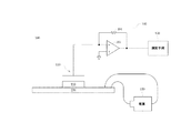
【解決手段】センサと、電源と、測定手段とを備えた検査装置である。センサはプリント回路の電子素子の上方に配置される。電源は電力をプリント回路に供給することで、プリント回路が起動する。測定手段はプリント回路が起動したとき、センサにより検知信号を測定する。
【選択図】図1
Description
(1)電子素子の上方にセンサを配置し、
(2)電力をプリント回路に供給して、プリント回路を起動し、
(3)プリント回路が起動したとき、センサにより検知信号を測定する、ステップを含む。
ステップ410:電子素子の上方にセンサを配置し、
ステップ420:電力をプリント回路に供給して、プリント回路を起動し、
ステップ430:プリント回路が起動したとき、センサにより検知信号を測定する。
ステップ440:所定の閾値を予め格納し、
ステップ450:検知信号が所定の閾値に符合しないときごとに、エラー条件を表示する、ステップを含む。
ステップ510:検知信号からピーク間電圧を検出し、
ステップ520:検知信号のデューティサイクルを検出し、
ステップ530:検出信号に基づいて、RMS電圧を計算し、
ステップ540:検出信号の波形をサンプリングする、ステップを含む。
ステップ550:ピーク間電圧を予め格納し、
ステップ555:前記検知信号がこの所定のピーク間電圧の閾値に符合しないときごとに、第1の相違状態を表示する、ステップを含む。
ステップ560:所定のデューティサイクルの閾値を予め格納し、
ステップ565:前記検知信号のデューティサイクルが所定のデューティサイクルの閾値に符合しないときごとに、第2の相違状態を表示する、ステップを含む。
ステップ570:所定のRMS電圧の閾値を予め格納し、
ステップ575:前記RMS電圧が所定のRMS電圧の閾値に符合しないときごとに、第3の相違状態を表示する。
ステップ580:所定の波形モデルを予め格納し、
ステップ585:検知信号の波形が所定の波形モデルに符合しないときごとに、第4の相違状態を表示する、ステップを含む。
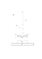
110 センサ
111 プローブ
112 プリント回路基板
113 プローブ
114 電線
115 平坦頭部
116 第1の面
117 第2の面
118 誘電体
120 電源
130 測定手段
140 記憶手段
150 監視手段
162 ピーク間電圧の検出モジュール
164 デューティサイクル検出モジュール
166 計算モジュール
168 サンプリングモジュール
171 第1の記憶モジュール
172 第1の表示モジュール
173 第2の記憶モジュール
174 第2の表示モジュール
175 第3の記憶モジュール
176 第3の表示モジュール
177 第4の記憶モジュール
178 第4の表示モジュール
191 信号源
193 ネガティブフィードバックアンプ
194 フィードバック抵抗
195 演算アンプ
200 プリント回路
210 電子素子
300 検査装置
310 第1の絶縁層
320 導電層
330 第2の絶縁層
390 信号バッファ
391 入力端
392 出力端
400 検査方法
410〜450 ステップ
510〜585 ステップ
Claims (10)
- 能動素子、受動素子または配線である少なくとも一つの電子素子を備えたプリント回路を検査するための検査装置であって、
前記電子素子の上方に配置されるセンサと、
前記プリント回路に電力を供給することで、前記プリント回路を起動する電源と、
前記プリント回路が起動したとき、前記センサにより検知信号を測定する測定手段と、を備えた、ことを特徴とする検査装置。 - 所定の閾値を予め格納している記憶手段と、
前記検知信号が前記所定の閾値に符合しないときごとに、エラー条件を表示する監視手段と、を更に備えた、ことを特徴とする請求項1に記載の検査装置。 - 前記検知信号からピーク間電圧を検出するピーク間電圧検出モジュールと、
所定のピーク間電圧の閾値を予め格納する第1の記憶モジュールと、
前記検知信号が前記所定のピーク間電圧の閾値に符合しないときごとに、第1の相違状態を表示する第1の表示モジュールと、
前記検知信号のデューティサイクルを検出するデューティサイクル検出モジュールと、
所定のデューティサイクルの閾値を予め格納する第2の記憶モジュールと、
前記検知信号のデューティサイクルが前記所定のデューティサイクルの閾値に符合しないときごとに、第2の相違状態を表示する第2の表示モジュールと、
前記検知信号に基づいて、RMS電圧を計算する計算モジュールと、
所定のRMS電圧の閾値を予め格納する第3の記憶モジュールと、
前記RMS電圧が前記所定のRMS電圧の閾値に符合しないときごとに、第3の相違状態を表示する第3の表示モジュールと、
前記検知信号の波形に対してサンプリングを行うサンプリングモジュールと、
所定の波形モデルを予め格納する第4の記憶モジュールと、
前記検知信号の波形が前記所定の波形モデルに符合しないときごとに、第4の相違状態を表示する第4の表示モジュールと、を更に備えた、ことを特徴とする請求項1に記載の検査装置。 - 前記センサが、
プローブと、
前記プローブに電気的に接続されているプリント回路基板と、を備えた、ことを特徴とする請求項1に記載の検査装置。 - 前記センサが、
前記プローブを覆う第1の絶縁層と、
前記第1の絶縁層を覆う導電層と、
前記導電層を覆う第2の絶縁層と、
前記導電層に電気的に接続されているリード線と、
前記プローブに電気的に接続されている入力端と、前記リード線を介して前記導電層に接続されている出力端とを有する信号バッファと、を更に備えた、ことを特徴とする請求項4に記載の検査装置。 - 前記センサが、
電線と、第1の面と第2の面とを有する平坦頭部とを有し、前記電線が前記平坦頭部の前記第1の面に電気的に接続されているプローブと、
前記平坦頭部の前記第2の面上に配設されている誘電体と、を備えた、ことを特徴とする請求項1に記載の検査装置。 - 前記センサが、
前記電線を覆う第1の絶縁層と、
前記第1の絶縁層を覆う導電層と、
前記導電層を覆う第2の絶縁層と、
前記導電層に電気的に接続されているリード線と、
前記電線に電気的に接続されている入力端と、前記リード線を介して前記導電層に接続されている出力端とを有する信号バッファと、を更に備えた、ことを特徴とする請求項6に記載の検査装置。 - 能動素子、受動素子または配線である少なくとも一つの電子素子を備えたプリント回路を検査するための検査方法であって、
前記電子素子の上方にセンサを配置するステップと、
電力を前記プリント回路に供給して、前記プリント回路を起動するステップと、
前記プリント回路が起動したとき、前記センサにより検知信号を測定するステップと、を含む、ことを特徴とする検査方法。 - 所定の閾値を予め格納するステップと、
前記検知信号が前記所定の閾値に符合しないときごとに、エラー条件を表示するステップと、を更に含む、ことを特徴とする請求項8に記載の検査方法。 - 前記検知信号からピーク間電圧を検出するステップと、
所定のピーク間電圧の閾値を予め格納するステップと、
前記検知信号が前記所定のピーク間電圧の閾値に符合しないときごとに、第1の相違状態を表示するステップと、
前記検知信号のデューティサイクルを検出するステップと、
所定のデューティサイクルの閾値を予め格納するステップと、
前記検知信号のデューティサイクルが前記所定のデューティサイクルの閾値に符合しないときごとに、第2の相違状態を表示するステップと、
前記検知信号に基づいて、RMS電圧を計算するステップと、
所定のRMS電圧の閾値を予め格納するステップと、
前記RMS電圧が前記所定のRMS電圧の閾値に符合しないときごとに、第3の相違状態を表示するステップと、
前記検知信号の波形に対してサンプリングを行うステップと、
所定の波形モデルを予め格納するステップと、
前記検知信号の波形前記が所定の波形モデルに符合しないときごとに、第4の相違状態を表示するステップと、を更に含む、ことを特徴とする請求項8に記載の検査方法。
Applications Claiming Priority (2)
| Application Number | Priority Date | Filing Date | Title |
|---|---|---|---|
| US12/251,892 | 2008-10-15 | ||
| US12/251,892 US8179143B2 (en) | 2008-10-15 | 2008-10-15 | Apparatus for testing printed circuit and method therefor |
Publications (2)
| Publication Number | Publication Date |
|---|---|
| JP2010096739A true JP2010096739A (ja) | 2010-04-30 |
| JP5231295B2 JP5231295B2 (ja) | 2013-07-10 |
Family
ID=41224951
Family Applications (1)
| Application Number | Title | Priority Date | Filing Date |
|---|---|---|---|
| JP2009056991A Active JP5231295B2 (ja) | 2008-10-15 | 2009-03-10 | 検査装置およびその検査方法 |
Country Status (4)
| Country | Link |
|---|---|
| US (1) | US8179143B2 (ja) |
| JP (1) | JP5231295B2 (ja) |
| CN (2) | CN201331567Y (ja) |
| TW (1) | TWI379089B (ja) |
Families Citing this family (5)
| Publication number | Priority date | Publication date | Assignee | Title |
|---|---|---|---|---|
| US8179143B2 (en) * | 2008-10-15 | 2012-05-15 | Test Research, Inc. | Apparatus for testing printed circuit and method therefor |
| TWI383160B (zh) * | 2009-12-31 | 2013-01-21 | Test Research Inc | 電性連接瑕疵偵測系統及方法 |
| US9523729B2 (en) * | 2013-09-13 | 2016-12-20 | Infineon Technologies Ag | Apparatus and method for testing electric conductors |
| TWI560454B (en) * | 2014-11-07 | 2016-12-01 | Primax Electronics Ltd | Testing base |
| CN116243141A (zh) * | 2022-12-31 | 2023-06-09 | 广东科翔电子科技股份有限公司 | Pcb快速检测方法、应用及装置 |
Citations (6)
| Publication number | Priority date | Publication date | Assignee | Title |
|---|---|---|---|---|
| JPH0328770A (ja) * | 1989-03-03 | 1991-02-06 | Nhk Spring Co Ltd | 導電性接触子 |
| JPH0465683A (ja) * | 1990-07-04 | 1992-03-02 | Denshi Seiki Kogyo Kk | コイル試験方法とその方法に用いる装置 |
| JPH08233894A (ja) * | 1995-01-11 | 1996-09-13 | Hewlett Packard Co <Hp> | 実装部品の極性判別方法 |
| JPH0980107A (ja) * | 1995-09-08 | 1997-03-28 | Aisin Aw Co Ltd | 電子制御式自動変速機のリニアソレノイド端子間ショートの検出方法 |
| JP2002098728A (ja) * | 2000-07-17 | 2002-04-05 | Matsushita Electric Ind Co Ltd | 漏電検出装置 |
| JP2004245709A (ja) * | 2003-02-14 | 2004-09-02 | Fuji Xerox Co Ltd | 故障診断方法、故障診断システム、故障診断装置 |
Family Cites Families (33)
| Publication number | Priority date | Publication date | Assignee | Title |
|---|---|---|---|---|
| US616935A (en) * | 1899-01-03 | Saw-setting machine | ||
| US3590378A (en) * | 1967-11-16 | 1971-06-29 | Gen Electric Information Syste | Fault-detecting monitor for integrated circuit units |
| US3870953A (en) * | 1972-08-01 | 1975-03-11 | Roger Boatman & Associates Inc | In circuit electronic component tester |
| US3825824A (en) * | 1973-06-01 | 1974-07-23 | Gte Automatic Electric Lab Inc | Matrix scanning circuit for testing a multiplicity of circuit paths |
| US3975680A (en) * | 1975-06-25 | 1976-08-17 | Honeywell Information Systems, Inc. | Non-contact coupling plate for circuit board tester |
| US4196386A (en) * | 1978-04-13 | 1980-04-01 | Ncr Corporation | Method and portable apparatus for testing digital printed circuit boards |
| US4565966A (en) * | 1983-03-07 | 1986-01-21 | Kollmorgen Technologies Corporation | Method and apparatus for testing of electrical interconnection networks |
| DE3526485A1 (de) * | 1985-07-24 | 1987-02-05 | Heinz Krug | Schaltungsanordnung zum pruefen integrierter schaltungseinheiten |
| US4894605A (en) * | 1988-02-24 | 1990-01-16 | Digital Equipment Corporation | Method and on-chip apparatus for continuity testing |
| US5138266A (en) * | 1989-10-20 | 1992-08-11 | Digital Equipment Corporation | Single-probe charge measurement testing method |
| US5124660A (en) * | 1990-12-20 | 1992-06-23 | Hewlett-Packard Company | Identification of pin-open faults by capacitive coupling through the integrated circuit package |
| US5254953A (en) * | 1990-12-20 | 1993-10-19 | Hewlett-Packard Company | Identification of pin-open faults by capacitive coupling through the integrated circuit package |
| US5557209A (en) * | 1990-12-20 | 1996-09-17 | Hewlett-Packard Company | Identification of pin-open faults by capacitive coupling through the integrated circuit package |
| EP0508062B1 (de) * | 1991-04-10 | 1995-07-19 | atg test systems GmbH | Verfahren und Vorrichtung zur Prüfung einer elektrischen Leiteranordnung |
| US5187430A (en) * | 1991-08-30 | 1993-02-16 | Compaq Computer Corporation | Method and apparatus for determining nets among nodes in a circuit board |
| US5457400A (en) * | 1992-04-10 | 1995-10-10 | Micron Technology, Inc. | Semiconductor array having built-in test circuit for wafer level testing |
| US5256975A (en) * | 1992-06-01 | 1993-10-26 | Digital Equipment Corporation | Manually-operated continuity/shorts test probe for bare interconnection packages |
| US5363048A (en) * | 1992-11-17 | 1994-11-08 | Digital Equipment Corporation | Method and system for ensuring interconnect integrity in a micro-chip-module |
| US5420500A (en) * | 1992-11-25 | 1995-05-30 | Hewlett-Packard Company | Pacitive electrode system for detecting open solder joints in printed circuit assemblies |
| US5391993A (en) * | 1994-01-27 | 1995-02-21 | Genrad, Inc. | Capacitive open-circuit test employing threshold determination |
| KR970011651B1 (ko) * | 1994-02-02 | 1997-07-12 | 삼성전자 주식회사 | 반도체 소자의 버스라인 블록화에 의한 단선 검사장치 및 검사방법 |
| US5831918A (en) * | 1994-02-14 | 1998-11-03 | Micron Technology, Inc. | Circuit and method for varying a period of an internal control signal during a test mode |
| KR0131389B1 (ko) * | 1994-09-27 | 1998-04-14 | 황인길 | 비지에이 반도체패키지의 와이어본딩 검사방법 |
| US5811980A (en) * | 1995-08-21 | 1998-09-22 | Genrad, Inc. | Test system for determining the orientation of components on a circuit board |
| US6104198A (en) * | 1997-05-20 | 2000-08-15 | Zen Licensing Group Llp | Testing the integrity of an electrical connection to a device using an onboard controllable signal source |
| US6144210A (en) * | 1998-06-09 | 2000-11-07 | Zen Licensing Group, Llp | Method and apparatus for finding and locating manufacturing defects on a printed circuit board |
| CN2629046Y (zh) * | 2003-05-26 | 2004-07-28 | 系新科技股份有限公司 | 印刷电路板的元件测试装置 |
| US6998849B2 (en) * | 2003-09-27 | 2006-02-14 | Agilent Technologies, Inc. | Capacitive sensor measurement method for discrete time sampled system for in-circuit test |
| WO2006043511A1 (ja) * | 2004-10-18 | 2006-04-27 | Nsk Ltd. | 機械設備の異常診断システム |
| CA2605356A1 (en) | 2005-08-29 | 2007-03-08 | Toyota Jidosha Kabushiki Kaisha | Insulation resistance drop detector and failure self-diagnosis method for insulation resistance drop detector |
| US7295031B1 (en) * | 2006-07-12 | 2007-11-13 | Agilent Technologies, Inc. | Method for non-contact testing of marginal integrated circuit connections |
| CN101261302B (zh) | 2007-03-08 | 2010-08-18 | 德律科技股份有限公司 | 电路开路检测系统及其方法 |
| US8179143B2 (en) * | 2008-10-15 | 2012-05-15 | Test Research, Inc. | Apparatus for testing printed circuit and method therefor |
-
2008
- 2008-10-15 US US12/251,892 patent/US8179143B2/en active Active
- 2008-12-08 TW TW097147718A patent/TWI379089B/zh active
- 2008-12-17 CN CNU2008201814308U patent/CN201331567Y/zh not_active Expired - Lifetime
- 2008-12-17 CN CN2008101862202A patent/CN101726683B/zh active Active
-
2009
- 2009-03-10 JP JP2009056991A patent/JP5231295B2/ja active Active
Patent Citations (6)
| Publication number | Priority date | Publication date | Assignee | Title |
|---|---|---|---|---|
| JPH0328770A (ja) * | 1989-03-03 | 1991-02-06 | Nhk Spring Co Ltd | 導電性接触子 |
| JPH0465683A (ja) * | 1990-07-04 | 1992-03-02 | Denshi Seiki Kogyo Kk | コイル試験方法とその方法に用いる装置 |
| JPH08233894A (ja) * | 1995-01-11 | 1996-09-13 | Hewlett Packard Co <Hp> | 実装部品の極性判別方法 |
| JPH0980107A (ja) * | 1995-09-08 | 1997-03-28 | Aisin Aw Co Ltd | 電子制御式自動変速機のリニアソレノイド端子間ショートの検出方法 |
| JP2002098728A (ja) * | 2000-07-17 | 2002-04-05 | Matsushita Electric Ind Co Ltd | 漏電検出装置 |
| JP2004245709A (ja) * | 2003-02-14 | 2004-09-02 | Fuji Xerox Co Ltd | 故障診断方法、故障診断システム、故障診断装置 |
Also Published As
| Publication number | Publication date |
|---|---|
| CN101726683B (zh) | 2013-01-16 |
| JP5231295B2 (ja) | 2013-07-10 |
| TWI379089B (en) | 2012-12-11 |
| TW201015082A (en) | 2010-04-16 |
| CN201331567Y (zh) | 2009-10-21 |
| US8179143B2 (en) | 2012-05-15 |
| US20100090679A1 (en) | 2010-04-15 |
| CN101726683A (zh) | 2010-06-09 |
Similar Documents
| Publication | Publication Date | Title |
|---|---|---|
| US7629796B2 (en) | Contact type single side probe device and apparatus and method for testing open or short circuits of conductive lines using the same | |
| US5124660A (en) | Identification of pin-open faults by capacitive coupling through the integrated circuit package | |
| US6937035B2 (en) | Method and apparatus for inspecting printed circuit boards | |
| EP0573159A2 (en) | Identification of pin-open faults by capacitive coupling through the integrated circuit package | |
| JP5231295B2 (ja) | 検査装置およびその検査方法 | |
| WO2011121862A1 (ja) | 静電容量式タッチパネルの検査装置、及び検査方法 | |
| JPH07191080A (ja) | 電気接続の完全性を測定するための装置と方法 | |
| JP2002156399A (ja) | 回路基板の検査装置及び検査方法 | |
| CN1996032A (zh) | 布线不良检查方法以及布线不良检查装置 | |
| JP2012149914A (ja) | プリント基板劣化検査装置および劣化検査方法 | |
| TWI474012B (zh) | 導電圖案檢查裝置及檢查方法 | |
| JP5452965B2 (ja) | ポゴタワー電気チャネル自己検査式半導体試験システム | |
| KR101430040B1 (ko) | 절연검사장치 및 절연검사방법 | |
| JP5420277B2 (ja) | 回路基板検査装置および回路基板検査方法 | |
| KR101039049B1 (ko) | 비접촉 검사방식을 적용한 단선 및 단락 검출용 칩 스케일 패키지 기판 및 그 검사장치 | |
| JP2002014132A (ja) | 回路基板検査装置 | |
| JP2004264147A (ja) | 静電気試験装置 | |
| TWI461711B (zh) | 決定電裝置特性之裝置與方法 | |
| JP2002131365A (ja) | 検査方法及び検査装置 | |
| JP4512264B2 (ja) | 検査方法及び検査装置 | |
| KR20140009027A (ko) | 기판 검사 장치 및 기판 검사 방법 | |
| JP5959204B2 (ja) | 実装状態判別装置および実装状態判別方法 | |
| EP1914558A2 (en) | Method to test transparent - to - test capacitors | |
| JPH11202016A (ja) | 回路基板の検査方法及び装置 | |
| KR20080092523A (ko) | 접촉식 싱글사이드 프로브와 이를 이용한 도선의 단선 및단락 검사장치 및 그 방법 |
Legal Events
| Date | Code | Title | Description |
|---|---|---|---|
| A131 | Notification of reasons for refusal |
Free format text: JAPANESE INTERMEDIATE CODE: A131 Effective date: 20111213 |
|
| A521 | Request for written amendment filed |
Free format text: JAPANESE INTERMEDIATE CODE: A523 Effective date: 20120312 |
|
| A131 | Notification of reasons for refusal |
Free format text: JAPANESE INTERMEDIATE CODE: A131 Effective date: 20121120 |
|
| A521 | Request for written amendment filed |
Free format text: JAPANESE INTERMEDIATE CODE: A523 Effective date: 20130213 |
|
| TRDD | Decision of grant or rejection written | ||
| A01 | Written decision to grant a patent or to grant a registration (utility model) |
Free format text: JAPANESE INTERMEDIATE CODE: A01 Effective date: 20130312 |
|
| A61 | First payment of annual fees (during grant procedure) |
Free format text: JAPANESE INTERMEDIATE CODE: A61 Effective date: 20130321 |
|
| FPAY | Renewal fee payment (event date is renewal date of database) |
Free format text: PAYMENT UNTIL: 20160329 Year of fee payment: 3 |
|
| R150 | Certificate of patent or registration of utility model |
Ref document number: 5231295 Country of ref document: JP Free format text: JAPANESE INTERMEDIATE CODE: R150 Free format text: JAPANESE INTERMEDIATE CODE: R150 |
|
| R250 | Receipt of annual fees |
Free format text: JAPANESE INTERMEDIATE CODE: R250 |
|
| R250 | Receipt of annual fees |
Free format text: JAPANESE INTERMEDIATE CODE: R250 |
|
| R250 | Receipt of annual fees |
Free format text: JAPANESE INTERMEDIATE CODE: R250 |
|
| R250 | Receipt of annual fees |
Free format text: JAPANESE INTERMEDIATE CODE: R250 |