JP2010073973A - 化合物半導体積層体及びその製造方法並びに半導体デバイス - Google Patents
化合物半導体積層体及びその製造方法並びに半導体デバイス Download PDFInfo
- Publication number
- JP2010073973A JP2010073973A JP2008241047A JP2008241047A JP2010073973A JP 2010073973 A JP2010073973 A JP 2010073973A JP 2008241047 A JP2008241047 A JP 2008241047A JP 2008241047 A JP2008241047 A JP 2008241047A JP 2010073973 A JP2010073973 A JP 2010073973A
- Authority
- JP
- Japan
- Prior art keywords
- compound semiconductor
- substrate
- layer
- laminate
- irradiated
- Prior art date
- Legal status (The legal status is an assumption and is not a legal conclusion. Google has not performed a legal analysis and makes no representation as to the accuracy of the status listed.)
- Granted
Links
- 239000004065 semiconductor Substances 0.000 title claims abstract description 109
- 150000001875 compounds Chemical class 0.000 title claims abstract description 99
- 238000004519 manufacturing process Methods 0.000 title claims abstract description 18
- 238000000034 method Methods 0.000 title abstract description 15
- 239000000758 substrate Substances 0.000 claims abstract description 119
- 239000013078 crystal Substances 0.000 claims abstract description 26
- 239000000463 material Substances 0.000 claims abstract description 13
- 239000010409 thin film Substances 0.000 claims abstract description 11
- 230000003287 optical effect Effects 0.000 claims abstract description 8
- 239000000126 substance Substances 0.000 claims description 22
- 229910052739 hydrogen Inorganic materials 0.000 claims description 19
- 239000001257 hydrogen Substances 0.000 claims description 19
- UFHFLCQGNIYNRP-UHFFFAOYSA-N Hydrogen Chemical compound [H][H] UFHFLCQGNIYNRP-UHFFFAOYSA-N 0.000 claims description 15
- 239000000470 constituent Substances 0.000 claims description 12
- 230000001678 irradiating effect Effects 0.000 claims description 7
- 150000002431 hydrogen Chemical class 0.000 claims description 4
- 239000010408 film Substances 0.000 abstract description 49
- 238000011161 development Methods 0.000 abstract description 3
- 239000010410 layer Substances 0.000 description 29
- 238000001004 secondary ion mass spectrometry Methods 0.000 description 16
- 238000002017 high-resolution X-ray diffraction Methods 0.000 description 13
- 150000002500 ions Chemical class 0.000 description 12
- KRHYYFGTRYWZRS-UHFFFAOYSA-N Fluorane Chemical compound F KRHYYFGTRYWZRS-UHFFFAOYSA-N 0.000 description 9
- 229910052733 gallium Inorganic materials 0.000 description 9
- 229910052757 nitrogen Inorganic materials 0.000 description 8
- 238000001451 molecular beam epitaxy Methods 0.000 description 7
- 229910052738 indium Inorganic materials 0.000 description 6
- 230000005540 biological transmission Effects 0.000 description 5
- 238000002003 electron diffraction Methods 0.000 description 5
- 238000000619 electron energy-loss spectrum Methods 0.000 description 5
- 229910001218 Gallium arsenide Inorganic materials 0.000 description 4
- 238000010586 diagram Methods 0.000 description 3
- 230000004907 flux Effects 0.000 description 3
- 230000015572 biosynthetic process Effects 0.000 description 2
- 230000000052 comparative effect Effects 0.000 description 2
- 238000002474 experimental method Methods 0.000 description 2
- 238000005259 measurement Methods 0.000 description 2
- 229910052594 sapphire Inorganic materials 0.000 description 2
- 239000010980 sapphire Substances 0.000 description 2
- 238000007740 vapor deposition Methods 0.000 description 2
- DDFHBQSCUXNBSA-UHFFFAOYSA-N 5-(5-carboxythiophen-2-yl)thiophene-2-carboxylic acid Chemical compound S1C(C(=O)O)=CC=C1C1=CC=C(C(O)=O)S1 DDFHBQSCUXNBSA-UHFFFAOYSA-N 0.000 description 1
- 229910002704 AlGaN Inorganic materials 0.000 description 1
- ZSBXGIUJOOQZMP-JLNYLFASSA-N Matrine Chemical compound C1CC[C@H]2CN3C(=O)CCC[C@@H]3[C@@H]3[C@H]2N1CCC3 ZSBXGIUJOOQZMP-JLNYLFASSA-N 0.000 description 1
- 230000001133 acceleration Effects 0.000 description 1
- 229910052785 arsenic Inorganic materials 0.000 description 1
- 238000003877 atomic layer epitaxy Methods 0.000 description 1
- 229910052799 carbon Inorganic materials 0.000 description 1
- 238000006243 chemical reaction Methods 0.000 description 1
- 238000012790 confirmation Methods 0.000 description 1
- 230000007547 defect Effects 0.000 description 1
- 238000003795 desorption Methods 0.000 description 1
- 238000001514 detection method Methods 0.000 description 1
- 238000000921 elemental analysis Methods 0.000 description 1
- 229910000040 hydrogen fluoride Inorganic materials 0.000 description 1
- 238000010884 ion-beam technique Methods 0.000 description 1
- 239000002184 metal Substances 0.000 description 1
- 229910052751 metal Inorganic materials 0.000 description 1
- 150000004767 nitrides Chemical class 0.000 description 1
- 239000002096 quantum dot Substances 0.000 description 1
- 239000002356 single layer Substances 0.000 description 1
Images


Landscapes
- Physical Vapour Deposition (AREA)
- Physical Deposition Of Substances That Are Components Of Semiconductor Devices (AREA)
Abstract
【解決手段】Si基板1上に、InxGayAlzN(x,y,z:0以上、1以下)である活性層2が直接形成されている。この活性層2とSi基板1の単結晶層の界面にAsを含む物質が島状に存在している。Si基板1は、バルク単結晶基板又は最上層がSiである薄膜基板である。
【選択図】図1
Description
図1は、本発明の化合物半導体積層体の断面構造模式図で、図中符号1はSi基板、2はInxGayAlzN(x,y,z:0以上1以下)膜(化合物半導体層)を示している。本発明の化合物半導体積層体は、Si基板1上に、InxGayAlzN(x,y,z:0以上、1以下)2が直接形成されている。この化合物半導体層2とSi基板1の単結晶層の界面にAsを含む物質が島状に存在している。
図2は、本発明の化合物半導体積層体の実施例1に係る製造方法を説明するための工程フロー図である。まず、直径4インチの(111)Si基板を洗浄後、1wt%のフッ化水素酸で処理して水素終端させた。次いで、分子線エピタキシー(MBE)装置にSi基板1を導入した。Si基板を成長室に導入する前に、Asを10秒成長室に供給した(ステップS21)。Asは、イオンゲージで測定したフラックスで10-5Torr台とした。続いて、成長室に前記Si基板を導入した(ステップS22)。
図2の工程フローで、ステップ21のみを省いて,実施例1と同じ実験を行なった。すなわち、まず、直径4インチの(111)Si基板を洗浄後、1wt%のフッ化水素酸で処理して水素終端させた。次いで、分子線エピタキシー(MBE)装置にSi基板1を導入した。
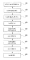
図3は、本発明の化合物半導体積層体の実施例2に係る製造方法を説明するための工程フロー図である。まず、直径4インチの(111)Si基板を洗浄後、1wt%のフッ化水素酸で処理して水素終端させた。次いで、分子線エピタキシー(MBE)装置にSi基板1を導入した。Si基板を成長室に導入する前に、Asを10秒成長室に供給した(ステップS31)。Asは、イオンゲージで測定したフラックスで10-5Torr台とした。続いて、成長室に前記Si基板を導入した(ステップS32)。
図3の工程フローで、ステップ31のみを省いて、実施例2と同じ実験を行なった。すなわち、まず、直径4インチの(111)Si基板を洗浄後、1wt%のフッ化水素酸で処理して水素終端させた。次いで、分子線エピタキシー(MBE)装置にSi基板1を導入した。
2 InxGayAlzN(x,y,z:0以上、1以下)膜(化合物半導体層)
Claims (14)
- Si基板上に、InxGayAlzN(x,y,z:0以上、1以下)を直接形成してなる化合物半導体積層体において、前記化合物半導体層と前記Si基板の界面にAsを含む物質が、島状に存在することを特徴とする化合物半導体積層体。
- 前記化合物半導体層が、活性層であることを特徴とする請求項1に記載の化合物半導体積層体。
- 前記島状物質は、前記Si基板又は前記化合物半導体層の構成元素の一部から成ることを特徴とする請求項1又は2に記載の化合物半導体積層体。
- 前記島状物質が、前記Si基板に対してエピタキシャル成長していないことを特徴とする請求項1,2又は3に記載の化合物半導体積層体。
- 前記島状物質が、前記Si基板及び前記化合物半導体層と結晶配列が異なることを特徴とする請求項1乃至4のいずれかに記載の化合物半導体積層体。
- 前記化合物半導体が、単結晶薄膜であることを特徴とする請求項1乃至5のいずれかに記載の化合物半導体積層体。
- 前記活性層の膜厚が、0.1μm以上、5μm以下であることを特徴とする請求項1乃至6のいずれかに記載の化合物半導体積層体。
- あらゆる位置における化合物半導体層の結晶の質が均一であることを特徴とする請求項7に記載の化合物半導体積層体。
- Si基板上に化合物半導体を形成する化合物半導体積層体の製造方法において、
前記Si基板を水素終端させ、次いで、該Si基板上にAsを先行して照射して、次いで、Siから水素が脱離する前に化合物半導体の構成物質を照射して化合物半導体を形成することを特徴とする化合物半導体積層体の製造方法。 - Si基板上に化合物半導体を形成する化合物半導体積層体の製造方法において、前記Si基板を水素終端させ、次いで、該Si基板上に直接Asを照射せずに、雰囲気にAsを存在させ、次いで、Siから水素が脱離する前に化合物半導体の構成物質を照射して化合物半導体を形成することを特徴とする化合物半導体積層体の製造方法。
- 前記化合物半導体の構成物質を前記Si基板に照射して薄膜を形成した後に、前記Si基板の温度を上昇させ、次いで、前記化合物半導体の構成物質を照射することを特徴とする請求項9又は10に記載の化合物半導体積層体の製造方法。
- 前記Si基板が、バルク単結晶基板又は最上層がSiである薄膜基板であることを特徴とする請求項9,10又は11に記載の化合物半導体積層体の製造方法。
- 請求項1乃至8のいずれかに記載の化合物半導体積層体にオーミック電極が形成されてなることを特徴とする半導体デバイス。
- 前記半導体デバイスが、電子デバイス,光デバイスのいずれかであることを特徴とする請求項13に記載の半導体デバイス。
Priority Applications (1)
| Application Number | Priority Date | Filing Date | Title |
|---|---|---|---|
| JP2008241047A JP5272160B2 (ja) | 2008-09-19 | 2008-09-19 | 化合物半導体積層体及び半導体デバイス |
Applications Claiming Priority (1)
| Application Number | Priority Date | Filing Date | Title |
|---|---|---|---|
| JP2008241047A JP5272160B2 (ja) | 2008-09-19 | 2008-09-19 | 化合物半導体積層体及び半導体デバイス |
Publications (2)
| Publication Number | Publication Date |
|---|---|
| JP2010073973A true JP2010073973A (ja) | 2010-04-02 |
| JP5272160B2 JP5272160B2 (ja) | 2013-08-28 |
Family
ID=42205478
Family Applications (1)
| Application Number | Title | Priority Date | Filing Date |
|---|---|---|---|
| JP2008241047A Active JP5272160B2 (ja) | 2008-09-19 | 2008-09-19 | 化合物半導体積層体及び半導体デバイス |
Country Status (1)
| Country | Link |
|---|---|
| JP (1) | JP5272160B2 (ja) |
Citations (2)
| Publication number | Priority date | Publication date | Assignee | Title |
|---|---|---|---|---|
| JPH0794409A (ja) * | 1993-09-20 | 1995-04-07 | Fujitsu Ltd | Iii−v族化合物半導体薄膜の形成方法 |
| JPH09162125A (ja) * | 1995-12-11 | 1997-06-20 | Mitsubishi Electric Corp | 半導体装置,及びその製造方法 |
-
2008
- 2008-09-19 JP JP2008241047A patent/JP5272160B2/ja active Active
Patent Citations (2)
| Publication number | Priority date | Publication date | Assignee | Title |
|---|---|---|---|---|
| JPH0794409A (ja) * | 1993-09-20 | 1995-04-07 | Fujitsu Ltd | Iii−v族化合物半導体薄膜の形成方法 |
| JPH09162125A (ja) * | 1995-12-11 | 1997-06-20 | Mitsubishi Electric Corp | 半導体装置,及びその製造方法 |
Also Published As
| Publication number | Publication date |
|---|---|
| JP5272160B2 (ja) | 2013-08-28 |
Similar Documents
| Publication | Publication Date | Title |
|---|---|---|
| JP5401706B2 (ja) | 化合物半導体積層体及びその製造方法並びに半導体デバイス | |
| US20120058626A1 (en) | Method for manufacturing nitride semiconductor crystal layer | |
| EP2544220A1 (en) | Single crystal substrate, production method for single crystal substrate, production method for single crystal substrate with multilayer film, and device production method | |
| CN108140563A (zh) | 半导体元件用外延基板、半导体元件和半导体元件用外延基板的制造方法 | |
| JP6019129B2 (ja) | Iii族窒化物基板の処理方法およびエピタキシャル基板の製造方法 | |
| WO2018101367A1 (ja) | 半導体基板 | |
| WO2016013262A1 (ja) | 窒化ガリウム基板 | |
| JP5272160B2 (ja) | 化合物半導体積層体及び半導体デバイス | |
| JP6910345B2 (ja) | n型電極、該n型電極の製造方法、及び該n型電極をn型III族窒化物単結晶層上に備えたn型積層構造体 | |
| KR101088985B1 (ko) | 화합물 반도체 기판, 화합물 반도체 기판의 제조 방법 및 반도체 디바이스 | |
| CN114651084A (zh) | 层叠膜结构体和其制造方法 | |
| CN112420871A (zh) | 台面型铟镓砷探测器芯片及其制备方法 | |
| WO2018066289A1 (ja) | 半導体素子用基板、エッチング方法、及びエッチング液 | |
| Bah et al. | Assessing the electrical activity of individual ZnO nanowires thermally annealed in air | |
| JP6614486B2 (ja) | 紫外線受光素子 | |
| JP2021034504A (ja) | 窒化物半導体発光素子 | |
| Lingaparthi | Studies on GaN based HEMT heterostructures on 100-mm silicon grown by molecular beam epitaxy | |
| Yang | Epitaxial Transition Metal Dichalcogenide Films on GaN: Growth in High Vacuum and Characterization | |
| Matthews | Overcoming Longstanding Synthesis Challenges Toward Realizing the Full Device Potential of III-Nitride Semiconductors | |
| Allaparthi | Integrated and Monolithic III-Nitride Devices Grown by MBE | |
| Hasan | Heterogeneous Integration of Dissimilar Semiconductors: From Theory to the Experiment | |
| JP5583610B2 (ja) | 半導体素子用エピタキシャル基板および半導体素子 | |
| JP6050595B2 (ja) | 化合物半導体基板及びその製造方法 | |
| Eibelhuber et al. | Heterogeneous integration through direct wafer bonding | |
| Choi et al. | Thermally Stable Indium Contact to N-polar n-GaN for Reliable Vertical Light Emitting Diodes |
Legal Events
| Date | Code | Title | Description |
|---|---|---|---|
| A621 | Written request for application examination |
Free format text: JAPANESE INTERMEDIATE CODE: A621 Effective date: 20110803 |
|
| A977 | Report on retrieval |
Free format text: JAPANESE INTERMEDIATE CODE: A971007 Effective date: 20130212 |
|
| A131 | Notification of reasons for refusal |
Free format text: JAPANESE INTERMEDIATE CODE: A131 Effective date: 20130215 |
|
| RD13 | Notification of appointment of power of sub attorney |
Free format text: JAPANESE INTERMEDIATE CODE: A7433 Effective date: 20130308 |
|
| A521 | Written amendment |
Free format text: JAPANESE INTERMEDIATE CODE: A821 Effective date: 20130308 Free format text: JAPANESE INTERMEDIATE CODE: A523 Effective date: 20130326 |
|
| TRDD | Decision of grant or rejection written | ||
| A01 | Written decision to grant a patent or to grant a registration (utility model) |
Free format text: JAPANESE INTERMEDIATE CODE: A01 Effective date: 20130416 |
|
| A61 | First payment of annual fees (during grant procedure) |
Free format text: JAPANESE INTERMEDIATE CODE: A61 Effective date: 20130417 |
|
| R150 | Certificate of patent or registration of utility model |
Free format text: JAPANESE INTERMEDIATE CODE: R150 Ref document number: 5272160 Country of ref document: JP Free format text: JAPANESE INTERMEDIATE CODE: R150 |
|
| S531 | Written request for registration of change of domicile |
Free format text: JAPANESE INTERMEDIATE CODE: R313531 |
|
| R350 | Written notification of registration of transfer |
Free format text: JAPANESE INTERMEDIATE CODE: R350 |