JP2010057005A - Dll回路 - Google Patents
Dll回路 Download PDFInfo
- Publication number
- JP2010057005A JP2010057005A JP2008221064A JP2008221064A JP2010057005A JP 2010057005 A JP2010057005 A JP 2010057005A JP 2008221064 A JP2008221064 A JP 2008221064A JP 2008221064 A JP2008221064 A JP 2008221064A JP 2010057005 A JP2010057005 A JP 2010057005A
- Authority
- JP
- Japan
- Prior art keywords
- circuit
- setting information
- signal
- delay unit
- delay
- Prior art date
- Legal status (The legal status is an assumption and is not a legal conclusion. Google has not performed a legal analysis and makes no representation as to the accuracy of the status listed.)
- Granted
Links
Images


Classifications
-
- H—ELECTRICITY
- H03—ELECTRONIC CIRCUITRY
- H03L—AUTOMATIC CONTROL, STARTING, SYNCHRONISATION OR STABILISATION OF GENERATORS OF ELECTRONIC OSCILLATIONS OR PULSES
- H03L7/00—Automatic control of frequency or phase; Synchronisation
- H03L7/06—Automatic control of frequency or phase; Synchronisation using a reference signal applied to a frequency- or phase-locked loop
- H03L7/08—Details of the phase-locked loop
- H03L7/0805—Details of the phase-locked loop the loop being adapted to provide an additional control signal for use outside the loop
-
- H—ELECTRICITY
- H03—ELECTRONIC CIRCUITRY
- H03L—AUTOMATIC CONTROL, STARTING, SYNCHRONISATION OR STABILISATION OF GENERATORS OF ELECTRONIC OSCILLATIONS OR PULSES
- H03L7/00—Automatic control of frequency or phase; Synchronisation
- H03L7/06—Automatic control of frequency or phase; Synchronisation using a reference signal applied to a frequency- or phase-locked loop
- H03L7/08—Details of the phase-locked loop
- H03L7/081—Details of the phase-locked loop provided with an additional controlled phase shifter
- H03L7/0812—Details of the phase-locked loop provided with an additional controlled phase shifter and where no voltage or current controlled oscillator is used
- H03L7/0814—Details of the phase-locked loop provided with an additional controlled phase shifter and where no voltage or current controlled oscillator is used the phase shifting device being digitally controlled
-
- H—ELECTRICITY
- H03—ELECTRONIC CIRCUITRY
- H03L—AUTOMATIC CONTROL, STARTING, SYNCHRONISATION OR STABILISATION OF GENERATORS OF ELECTRONIC OSCILLATIONS OR PULSES
- H03L7/00—Automatic control of frequency or phase; Synchronisation
- H03L7/06—Automatic control of frequency or phase; Synchronisation using a reference signal applied to a frequency- or phase-locked loop
- H03L7/08—Details of the phase-locked loop
- H03L7/081—Details of the phase-locked loop provided with an additional controlled phase shifter
- H03L7/0812—Details of the phase-locked loop provided with an additional controlled phase shifter and where no voltage or current controlled oscillator is used
- H03L7/0816—Details of the phase-locked loop provided with an additional controlled phase shifter and where no voltage or current controlled oscillator is used the controlled phase shifter and the frequency- or phase-detection arrangement being connected to a common input
Landscapes
- Stabilization Of Oscillater, Synchronisation, Frequency Synthesizers (AREA)
Abstract
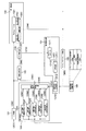
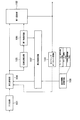
【解決手段】DLL回路は、入力信号に基づいて同期基準信号を生成する入力回路101と、同期基準信号を遅延する第1遅延部102と、第1遅延部102によって遅延された同期基準信号の同期位置を調整し、同期対象信号を生成するタイミングオフセット回路103と、同期基準信号と同期対象信号との位相差を比較する位相比較回路105と、位相比較回路105の比較結果に基づいて第1遅延部102の出力信号を選択する第1制御回路106と、同期基準信号又は同期対象信号を遅延する第2遅延部104と、所定の設定情報を記憶する設定情報記憶回路108と、位相比較回路105の比較結果が所定の範囲内である場合に、設定情報記憶回路108に記憶された設定情報に基づいて第2遅延部104の出力信号を選択する第2制御回路107と、を備えている。
【選択図】図1
Description
入力信号に基づいて同期基準信号を生成する入力回路と、
前記同期基準信号を遅延する第1遅延部と、
前記第1遅延部によって遅延された同期基準信号の同期位置を調整し、同期対象信号を生成するタイミングオフセット回路と、
前記同期基準信号と前記同期対象信号との位相差を比較する位相比較回路と、
前記位相比較回路の比較結果に基づいて前記第1遅延部の出力信号を選択する第1制御回路と、
前記同期基準信号又は前記同期対象信号を遅延する第2遅延部と、
所定の設定情報を記憶する設定情報記憶回路と、
前記位相比較回路の比較結果が所定の範囲内である場合に、前記設定情報記憶回路に記憶された設定情報に基づいて前記第2遅延部の出力信号を選択する第2制御回路と、を備えることを特徴とするDLL回路が提供される。
102 第1遅延部
1021 Delay Line
1022 選択回路
103 タイミングオフセット回路
104 第2遅延部
1041〜1045 遅延回路
1046 位相比較対象選択回路
105 位相比較回路
106 第1制御回路
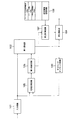
107 第2制御回路
1071 サイクルカウンタ
1072 比較回路
1073 選択信号生成回路
108 設定情報記憶回路
109 切替サイクル選択回路
Claims (5)
- 入力信号に基づいて同期基準信号を生成する入力回路と、
前記同期基準信号を遅延する第1遅延部と、
前記第1遅延部によって遅延された同期基準信号の同期位置を調整し、同期対象信号を生成するタイミングオフセット回路と、
前記同期基準信号と前記同期対象信号との位相差を比較する位相比較回路と、
前記位相比較回路の比較結果に基づいて前記第1遅延部の出力信号を選択する第1制御回路と、
前記同期基準信号又は前記同期対象信号を遅延する第2遅延部と、
所定の設定情報を記憶する設定情報記憶回路と、
前記位相比較回路の比較結果が所定の範囲内である場合に、前記設定情報記憶回路に記憶された設定情報に基づいて前記第2遅延部の出力信号を選択する第2制御回路と、を備えることを特徴とするDLL回路。 - 前記設定情報記憶回路は、アン・ロック状態のときに選択すべき前記第2遅延部の出力信号を示す設定情報を記憶する請求項1に記載のDLL回路。
- 前記設定情報記憶回路は、前記第2遅延部の出力信号の選択期間を示す設定情報を記憶する請求項1又は2に記載のDLL回路。
- 前記設定情報記憶回路は、前記第2制御回路のオン又はオフを示す設定情報を記憶する請求項1乃至3の何れか1項に記載のDLL回路。
- 前記設定情報記憶回路は、前記第2制御回路の一時停止期間を示す設定情報を記憶する請求項1乃至4の何れか1項に記載のDLL回路。
Priority Applications (2)
| Application Number | Priority Date | Filing Date | Title |
|---|---|---|---|
| JP2008221064A JP4703696B2 (ja) | 2008-08-29 | 2008-08-29 | Dll回路 |
| US12/475,269 US7821313B2 (en) | 2008-08-29 | 2009-05-29 | DLL circuit |
Applications Claiming Priority (1)
| Application Number | Priority Date | Filing Date | Title |
|---|---|---|---|
| JP2008221064A JP4703696B2 (ja) | 2008-08-29 | 2008-08-29 | Dll回路 |
Publications (2)
| Publication Number | Publication Date |
|---|---|
| JP2010057005A true JP2010057005A (ja) | 2010-03-11 |
| JP4703696B2 JP4703696B2 (ja) | 2011-06-15 |
Family
ID=41724421
Family Applications (1)
| Application Number | Title | Priority Date | Filing Date |
|---|---|---|---|
| JP2008221064A Expired - Fee Related JP4703696B2 (ja) | 2008-08-29 | 2008-08-29 | Dll回路 |
Country Status (2)
| Country | Link |
|---|---|
| US (1) | US7821313B2 (ja) |
| JP (1) | JP4703696B2 (ja) |
Families Citing this family (3)
| Publication number | Priority date | Publication date | Assignee | Title |
|---|---|---|---|---|
| KR20120012119A (ko) * | 2010-07-30 | 2012-02-09 | 주식회사 하이닉스반도체 | 레이턴시 제어 회로 및 그의 동작 방법 |
| KR20180110478A (ko) * | 2017-03-29 | 2018-10-10 | 에스케이하이닉스 주식회사 | 반도체 메모리 장치 및 테스트 방법 |
| US12237839B2 (en) * | 2022-08-22 | 2025-02-25 | Changxin Memory Technologies, Inc. | Delay locked loop and memory |
Citations (4)
| Publication number | Priority date | Publication date | Assignee | Title |
|---|---|---|---|---|
| JP2000306399A (ja) * | 1999-04-22 | 2000-11-02 | Mitsubishi Electric Corp | 半導体装置 |
| JP2003032105A (ja) * | 2001-06-29 | 2003-01-31 | Hynix Semiconductor Inc | クロック同期回路 |
| JP2005020083A (ja) * | 2003-06-23 | 2005-01-20 | Renesas Technology Corp | クロック発生回路 |
| JP2007006388A (ja) * | 2005-06-27 | 2007-01-11 | Toshiba Microelectronics Corp | 周波数逓倍回路 |
Family Cites Families (4)
| Publication number | Priority date | Publication date | Assignee | Title |
|---|---|---|---|---|
| JP2003032104A (ja) * | 2001-07-12 | 2003-01-31 | Mitsubishi Electric Corp | Dll回路とその制御方法 |
| JP3821787B2 (ja) * | 2003-02-27 | 2006-09-13 | エルピーダメモリ株式会社 | Dll回路 |
| JP4772733B2 (ja) * | 2007-04-13 | 2011-09-14 | 株式会社東芝 | Dll回路 |
| JP4861256B2 (ja) * | 2007-06-15 | 2012-01-25 | 株式会社東芝 | Dll回路 |
-
2008
- 2008-08-29 JP JP2008221064A patent/JP4703696B2/ja not_active Expired - Fee Related
-
2009
- 2009-05-29 US US12/475,269 patent/US7821313B2/en not_active Expired - Fee Related
Patent Citations (4)
| Publication number | Priority date | Publication date | Assignee | Title |
|---|---|---|---|---|
| JP2000306399A (ja) * | 1999-04-22 | 2000-11-02 | Mitsubishi Electric Corp | 半導体装置 |
| JP2003032105A (ja) * | 2001-06-29 | 2003-01-31 | Hynix Semiconductor Inc | クロック同期回路 |
| JP2005020083A (ja) * | 2003-06-23 | 2005-01-20 | Renesas Technology Corp | クロック発生回路 |
| JP2007006388A (ja) * | 2005-06-27 | 2007-01-11 | Toshiba Microelectronics Corp | 周波数逓倍回路 |
Also Published As
| Publication number | Publication date |
|---|---|
| US20100052750A1 (en) | 2010-03-04 |
| JP4703696B2 (ja) | 2011-06-15 |
| US7821313B2 (en) | 2010-10-26 |
Similar Documents
| Publication | Publication Date | Title |
|---|---|---|
| JP4774340B2 (ja) | パワーダウンモードの間、周期的にロッキング動作を実行する機能を有するdll及びそのロッキング動作方法 | |
| US9356611B1 (en) | Systems and methods involving phase detection with adaptive locking/detection features | |
| US7920001B2 (en) | Semiconductor memory device and method for operating the same | |
| US7889581B2 (en) | Digital DLL circuit | |
| JP2009278528A (ja) | Dll回路、および半導体装置 | |
| US8766688B2 (en) | DLL circuit and delay-locked method using the same | |
| JP4772733B2 (ja) | Dll回路 | |
| US8831064B1 (en) | Method of and circuit for generating a spread spectrum clock signal | |
| US8085072B2 (en) | Semiconductor integrated circuit having delay locked loop circuit | |
| JP4703696B2 (ja) | Dll回路 | |
| JP4769431B2 (ja) | ドットクロック同期生成回路 | |
| KR100878259B1 (ko) | 위상 검출기, 이를 포함하는 지연 고정 루프 및 이를구동하는 방법 | |
| US7003683B2 (en) | Glitchless clock selection circuit | |
| US8284880B2 (en) | Clock data recovery circuit and method for operating the same | |
| TWI536741B (zh) | 延遲鎖定迴路及包含其之積體電路 | |
| US6795516B1 (en) | Reset circuit and pll frequency synthesizer | |
| US7728640B2 (en) | DLL circuit | |
| US7848163B2 (en) | Semiconductor memory device and method for driving the same | |
| JP5326607B2 (ja) | 半導体装置 | |
| KR20130142743A (ko) | 지연 제어회로 및 이를 포함하는 클럭 생성회로 | |
| CN1797954B (zh) | 时钟信号产生装置及方法 | |
| JP2011242838A (ja) | メモリインタフェース回路 | |
| KR102709563B1 (ko) | 지연 고정 루프 | |
| JP2006074580A (ja) | Dll回路 | |
| JP2001177386A (ja) | 出力遅延調整回路 |
Legal Events
| Date | Code | Title | Description |
|---|---|---|---|
| A621 | Written request for application examination |
Free format text: JAPANESE INTERMEDIATE CODE: A621 Effective date: 20100803 |
|
| A977 | Report on retrieval |
Free format text: JAPANESE INTERMEDIATE CODE: A971007 Effective date: 20101014 |
|
| A131 | Notification of reasons for refusal |
Free format text: JAPANESE INTERMEDIATE CODE: A131 Effective date: 20101019 |
|
| A521 | Request for written amendment filed |
Free format text: JAPANESE INTERMEDIATE CODE: A523 Effective date: 20101207 |
|
| A01 | Written decision to grant a patent or to grant a registration (utility model) |
Free format text: JAPANESE INTERMEDIATE CODE: A01 Effective date: 20110215 |
|
| A61 | First payment of annual fees (during grant procedure) |
Free format text: JAPANESE INTERMEDIATE CODE: A61 Effective date: 20110308 |
|
| LAPS | Cancellation because of no payment of annual fees |