JP2010039105A - 光学フィルムおよびその製造方法ならびに表示装置 - Google Patents
光学フィルムおよびその製造方法ならびに表示装置 Download PDFInfo
- Publication number
- JP2010039105A JP2010039105A JP2008200671A JP2008200671A JP2010039105A JP 2010039105 A JP2010039105 A JP 2010039105A JP 2008200671 A JP2008200671 A JP 2008200671A JP 2008200671 A JP2008200671 A JP 2008200671A JP 2010039105 A JP2010039105 A JP 2010039105A
- Authority
- JP
- Japan
- Prior art keywords
- film
- light
- refractive index
- dimensional structure
- liquid crystalline
- Prior art date
- Legal status (The legal status is an assumption and is not a legal conclusion. Google has not performed a legal analysis and makes no representation as to the accuracy of the status listed.)
- Granted
Links
Images


Classifications
-
- G—PHYSICS
- G02—OPTICS
- G02F—OPTICAL DEVICES OR ARRANGEMENTS FOR THE CONTROL OF LIGHT BY MODIFICATION OF THE OPTICAL PROPERTIES OF THE MEDIA OF THE ELEMENTS INVOLVED THEREIN; NON-LINEAR OPTICS; FREQUENCY-CHANGING OF LIGHT; OPTICAL LOGIC ELEMENTS; OPTICAL ANALOGUE/DIGITAL CONVERTERS
- G02F1/00—Devices or arrangements for the control of the intensity, colour, phase, polarisation or direction of light arriving from an independent light source, e.g. switching, gating or modulating; Non-linear optics
- G02F1/01—Devices or arrangements for the control of the intensity, colour, phase, polarisation or direction of light arriving from an independent light source, e.g. switching, gating or modulating; Non-linear optics for the control of the intensity, phase, polarisation or colour
- G02F1/13—Devices or arrangements for the control of the intensity, colour, phase, polarisation or direction of light arriving from an independent light source, e.g. switching, gating or modulating; Non-linear optics for the control of the intensity, phase, polarisation or colour based on liquid crystals, e.g. single liquid crystal display cells
- G02F1/133—Constructional arrangements; Operation of liquid crystal cells; Circuit arrangements
- G02F1/1333—Constructional arrangements; Manufacturing methods
- G02F1/1335—Structural association of cells with optical devices, e.g. polarisers or reflectors
- G02F1/1336—Illuminating devices
- G02F1/133602—Direct backlight
- G02F1/133606—Direct backlight including a specially adapted diffusing, scattering or light controlling members
-
- G—PHYSICS
- G02—OPTICS
- G02B—OPTICAL ELEMENTS, SYSTEMS OR APPARATUS
- G02B5/00—Optical elements other than lenses
- G02B5/30—Polarising elements
- G02B5/3016—Polarising elements involving passive liquid crystal elements
-
- G—PHYSICS
- G02—OPTICS
- G02F—OPTICAL DEVICES OR ARRANGEMENTS FOR THE CONTROL OF LIGHT BY MODIFICATION OF THE OPTICAL PROPERTIES OF THE MEDIA OF THE ELEMENTS INVOLVED THEREIN; NON-LINEAR OPTICS; FREQUENCY-CHANGING OF LIGHT; OPTICAL LOGIC ELEMENTS; OPTICAL ANALOGUE/DIGITAL CONVERTERS
- G02F1/00—Devices or arrangements for the control of the intensity, colour, phase, polarisation or direction of light arriving from an independent light source, e.g. switching, gating or modulating; Non-linear optics
- G02F1/01—Devices or arrangements for the control of the intensity, colour, phase, polarisation or direction of light arriving from an independent light source, e.g. switching, gating or modulating; Non-linear optics for the control of the intensity, phase, polarisation or colour
- G02F1/13—Devices or arrangements for the control of the intensity, colour, phase, polarisation or direction of light arriving from an independent light source, e.g. switching, gating or modulating; Non-linear optics for the control of the intensity, phase, polarisation or colour based on liquid crystals, e.g. single liquid crystal display cells
- G02F1/133—Constructional arrangements; Operation of liquid crystal cells; Circuit arrangements
- G02F1/1333—Constructional arrangements; Manufacturing methods
- G02F1/1335—Structural association of cells with optical devices, e.g. polarisers or reflectors
- G02F1/133504—Diffusing, scattering, diffracting elements
- G02F1/133507—Films for enhancing the luminance
-
- G—PHYSICS
- G02—OPTICS
- G02F—OPTICAL DEVICES OR ARRANGEMENTS FOR THE CONTROL OF LIGHT BY MODIFICATION OF THE OPTICAL PROPERTIES OF THE MEDIA OF THE ELEMENTS INVOLVED THEREIN; NON-LINEAR OPTICS; FREQUENCY-CHANGING OF LIGHT; OPTICAL LOGIC ELEMENTS; OPTICAL ANALOGUE/DIGITAL CONVERTERS
- G02F1/00—Devices or arrangements for the control of the intensity, colour, phase, polarisation or direction of light arriving from an independent light source, e.g. switching, gating or modulating; Non-linear optics
- G02F1/01—Devices or arrangements for the control of the intensity, colour, phase, polarisation or direction of light arriving from an independent light source, e.g. switching, gating or modulating; Non-linear optics for the control of the intensity, phase, polarisation or colour
- G02F1/13—Devices or arrangements for the control of the intensity, colour, phase, polarisation or direction of light arriving from an independent light source, e.g. switching, gating or modulating; Non-linear optics for the control of the intensity, phase, polarisation or colour based on liquid crystals, e.g. single liquid crystal display cells
- G02F1/133—Constructional arrangements; Operation of liquid crystal cells; Circuit arrangements
- G02F1/1333—Constructional arrangements; Manufacturing methods
- G02F1/1335—Structural association of cells with optical devices, e.g. polarisers or reflectors
- G02F1/1336—Illuminating devices
- G02F1/133602—Direct backlight
- G02F1/133606—Direct backlight including a specially adapted diffusing, scattering or light controlling members
- G02F1/133607—Direct backlight including a specially adapted diffusing, scattering or light controlling members the light controlling member including light directing or refracting elements, e.g. prisms or lenses
-
- G—PHYSICS
- G02—OPTICS
- G02F—OPTICAL DEVICES OR ARRANGEMENTS FOR THE CONTROL OF LIGHT BY MODIFICATION OF THE OPTICAL PROPERTIES OF THE MEDIA OF THE ELEMENTS INVOLVED THEREIN; NON-LINEAR OPTICS; FREQUENCY-CHANGING OF LIGHT; OPTICAL LOGIC ELEMENTS; OPTICAL ANALOGUE/DIGITAL CONVERTERS
- G02F2202/00—Materials and properties
- G02F2202/40—Materials having a particular birefringence, retardation
Landscapes
- Physics & Mathematics (AREA)
- Chemical & Material Sciences (AREA)
- Crystallography & Structural Chemistry (AREA)
- General Physics & Mathematics (AREA)
- Optics & Photonics (AREA)
- Nonlinear Science (AREA)
- Mathematical Physics (AREA)
- Liquid Crystal (AREA)
- Optical Elements Other Than Lenses (AREA)
- Polarising Elements (AREA)
- Laminated Bodies (AREA)
Abstract
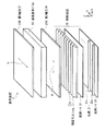
【解決手段】輝度向上フィルム33は、一の方向に延在すると共に上記一の方向と交差する方向に連続して配置された複数の凸部33aを備えている。凸部33aは、配向性を有する液晶性高分子を含んで構成されている。また、凸部33aは、当該凸部33aの延在方向の屈折率が当該凸部33aの延在方向と交差する方向の屈折率よりも小さな屈折率異方性を有しており、輝度向上フィルム33の偏光軸が凸部33aの延在方向と平行な方向に向いている。
【選択図】図1
Description
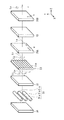
(A)一の方向に延在すると共に一の方向と交差する方向に連続して配置された複数の立体構造を備えた原盤と、原盤の立体構造と対向配置された光透過フィルムとの間に、ロッド状の液晶性モノマと光重合開始剤とを含む組成物を保持した状態で、組成物を、ロッド状の液晶性モノマの融点以上の温度で加熱し、かつ押圧ローラを光透過フィルム接触させると共に、原盤の立体構造の配列方向に転がすことにより組成物を押圧する第1工程
(B)組成物を常温まで冷やしたのち、組成物に対して紫外線を照射して、ロッド状の液晶性モノマを重合させ、光透過フィルムを原盤から剥離する第2工程
次に、上記実施の形態の輝度向上フィルム33の実施例1,2について比較例1,2,3と対比して説明する。実施例1,2および比較例2,3では、製造過程で用いられる組成物110にロッド状の液晶性モノマを含ませた。実施例1、比較例2ではロッド状の液晶性モノマとして高Δnタイプを使用し、実施例2、比較例3ではロッド状の液晶性モノマとして低Δnタイプを使用した。比較例1では、ロッド状の液晶性モノマの代わりに光硬化アクリルモノマを組成物110に含ませた。また、実施例および比較例1では、製造過程における押圧の方向を原盤100の凸部100a(または温調ロール250の凸部)の配列方向にし、比較例2では、製造過程における押圧の方向を原盤100の凸部100a(または温調ロール250の凸部)の延在方向にした。
輝度向上フィルムの配列方向の断面を走査型共焦点レーザ顕微鏡(LEXT OLS3000、オリンパス(株)製)で測定した。その結果、実施例1,2および比較例1,2,3において、輝度向上フィルムの断面はそれぞれ、原盤100の凹凸形状と同じ頂角90度、底角45度の直角二等辺三角形となっていた。このことから、輝度向上フィルムの凸部には形状の崩れが無いことがわかった。
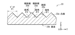
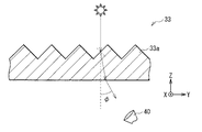
次に、輝度向上フィルムの複屈折性を測定した。複屈折性の測定には、図11に示すように、輝度向上フィルム33の凸部33a側から偏光を垂直に入射し、透過光を測定器40で検出し、透過光の出射角φの違いにより、凸部33aの延在方向の屈折率nxと配列方向の屈折率nyとの差Δn(=nx−ny)を算出した。なお、図12に示したように、凸部33aの延在方向に振動する偏光成分を垂直偏光Lxとし、凸部33aの配列方向に振動する偏光成分を水平偏光Lyとすると、垂直偏光Lxの射出角φxの方が水平偏光Lyの射出角φyよりも小さくなった。
Claims (7)
- 一の方向に延在すると共に前記一の方向と交差する方向に連続して配置された複数の立体構造を備え、
前記立体構造は、配向性を有する液晶性高分子を含み、かつ当該立体構造の延在方向の屈折率が当該立体構造の延在方向と交差する方向の屈折率よりも小さな屈折率異方性を有する光学フィルム。 - 前記液晶性高分子は、当該立体構造の配列方向に配向性を有するロッド状の液晶性モノマと光重合開始剤とを含む組成物に対して紫外線を照射して、ロッド状の液晶性モノマを重合させることにより形成されたものである請求項1に記載の光学フィルム。
- 前記立体構造は、多角柱状のプリズム、または突状の曲面を含むレンチキュラーレンズである請求項1に記載の光学フィルム。
- 光透過フィルムと、
前記光透過フィルム上に形成された光学機能層と
を備え、
前記立体構造は、前記光学機能層のうち前記光透過フィルムとは反対側の表面に形成され、
前記光学機能層のうち前記立体構造と前記光透過フィルムとの間の部分の厚さは、前記立体構造の高さの40%以下となっている請求項1に記載の光学フィルム。 - 一の方向に延在すると共に前記一の方向と交差する方向に連続して配置された複数の立体構造を備えた原盤と、前記原盤の立体構造と対向配置された光透過フィルムとの間に、ロッド状の液晶性モノマと光重合開始剤とを含む組成物を保持した状態で、前記組成物を、前記ロッド状の液晶性モノマの融点以上の温度で加熱し、かつ押圧ローラを前記光透過フィルム接触させると共に、前記原盤の立体構造の配列方向に転がすことにより前記組成物を押圧する第1工程と、
前記組成物を常温まで冷やしたのち、前記組成物に対して紫外線を照射して、前記ロッド状の液晶性モノマを重合させ、前記光透過フィルムを前記原盤から剥離する第2工程と
を含む光学フィルムの製造方法。 - 画像信号に基づいて駆動されるパネルと、
前記表示パネルを挟む一対の偏光子と、
前記パネルを照明する光源と、
前記偏光子と光源との間に設けられた光学フィルムと
を備え、
前記光学フィルムは、
一の方向に延在すると共に前記一の方向と交差する方向に連続して配置された複数の立体構造を備え、
前記立体構造は、配向性を有する液晶性高分子を含み、かつ当該立体構造の延在方向の屈折率が当該立体構造の延在方向と交差する方向の屈折率よりも小さな屈折率異方性を有する表示装置。 - 前記立体構造における屈折率の最も小さな方向が前記光源側の偏光子の光透過軸の方向と平行となっているか、または0度より大きく45度より小さな範囲内で交差している
ことを特徴とする請求項6に記載の表示装置。
Priority Applications (3)
| Application Number | Priority Date | Filing Date | Title |
|---|---|---|---|
| JP2008200671A JP5217747B2 (ja) | 2008-08-04 | 2008-08-04 | 光学フィルムおよびその製造方法ならびに表示装置 |
| US12/534,989 US8400578B2 (en) | 2008-08-04 | 2009-08-04 | Optical film, method of manufacturing the same, and display unit |
| CN2009101640220A CN101644851B (zh) | 2008-08-04 | 2009-08-04 | 光学膜及其制造方法以及显示单元 |
Applications Claiming Priority (1)
| Application Number | Priority Date | Filing Date | Title |
|---|---|---|---|
| JP2008200671A JP5217747B2 (ja) | 2008-08-04 | 2008-08-04 | 光学フィルムおよびその製造方法ならびに表示装置 |
Publications (2)
| Publication Number | Publication Date |
|---|---|
| JP2010039105A true JP2010039105A (ja) | 2010-02-18 |
| JP5217747B2 JP5217747B2 (ja) | 2013-06-19 |
Family
ID=41607809
Family Applications (1)
| Application Number | Title | Priority Date | Filing Date |
|---|---|---|---|
| JP2008200671A Expired - Fee Related JP5217747B2 (ja) | 2008-08-04 | 2008-08-04 | 光学フィルムおよびその製造方法ならびに表示装置 |
Country Status (3)
| Country | Link |
|---|---|
| US (1) | US8400578B2 (ja) |
| JP (1) | JP5217747B2 (ja) |
| CN (1) | CN101644851B (ja) |
Cited By (1)
| Publication number | Priority date | Publication date | Assignee | Title |
|---|---|---|---|---|
| JP2013061518A (ja) * | 2011-09-14 | 2013-04-04 | Dainippon Printing Co Ltd | プリズムシート型の製造方法、及び帯状の偏光子一体型プリズムシート |
Families Citing this family (2)
| Publication number | Priority date | Publication date | Assignee | Title |
|---|---|---|---|---|
| JP5991053B2 (ja) * | 2011-10-04 | 2016-09-14 | ソニー株式会社 | 表示装置および照明装置 |
| CN108459439B (zh) * | 2018-05-16 | 2023-11-17 | 京东方科技集团股份有限公司 | 背光模组及液晶显示装置 |
Citations (9)
| Publication number | Priority date | Publication date | Assignee | Title |
|---|---|---|---|---|
| JP2000221324A (ja) * | 1999-02-03 | 2000-08-11 | Nec Corp | 偏光素子、および該偏光素子を有する液晶表示装置 |
| JP2004037480A (ja) * | 2002-06-28 | 2004-02-05 | Asahi Glass Co Ltd | 液晶素子および光減衰器 |
| JP2006119258A (ja) * | 2004-10-20 | 2006-05-11 | Dainippon Printing Co Ltd | 真偽判定体及び真偽判定用ラベル |
| JP2007041583A (ja) * | 2005-07-30 | 2007-02-15 | Samsung Electronics Co Ltd | 偏光補償フィルム、偏光プリズムフィルムの製造方法、表示パネルアセンブリ、及び表示装置 |
| JP2007206104A (ja) * | 2006-01-30 | 2007-08-16 | Fujifilm Corp | 偏光変換フィルム及びその製造方法、偏光素子、並びに液晶表示装置 |
| JP2007213057A (ja) * | 2006-02-08 | 2007-08-23 | Samsung Electronics Co Ltd | 偏光導光板及びその製造方法、前記偏光導光板を利用した平板表示装置用の照明装置 |
| JP2007256493A (ja) * | 2006-03-22 | 2007-10-04 | Sony Corp | 光学シート、光学シートの製造方法、バックライト装置および液晶表示装置 |
| JP2008525230A (ja) * | 2004-12-23 | 2008-07-17 | スリーエム イノベイティブ プロパティズ カンパニー | 構造化表面を有する1軸配向複屈折物品 |
| JP2009109840A (ja) * | 2007-10-31 | 2009-05-21 | Sony Corp | 光学シートおよびその製造方法ならびに表示装置 |
Family Cites Families (6)
| Publication number | Priority date | Publication date | Assignee | Title |
|---|---|---|---|---|
| JPH01273002A (ja) | 1988-04-26 | 1989-10-31 | Seiko Epson Corp | 複屈折レンズアレイ |
| JPH071428U (ja) * | 1993-06-04 | 1995-01-10 | 株式会社エンプラス | 面光源装置 |
| JP2004198725A (ja) * | 2002-12-18 | 2004-07-15 | Sumitomo Rubber Ind Ltd | 液晶表示装置、直下型バックライト、及び拡散板 |
| CN100462750C (zh) * | 2004-10-27 | 2009-02-18 | 柯尼卡美能达精密光学株式会社 | 相位差膜的制造方法和用该方法制造的相位差膜、以及用其的偏振片和液晶显示装置 |
| US20060138702A1 (en) | 2004-12-23 | 2006-06-29 | Biernath Rolf W | Method of making uniaxially oriented articles having structured surfaces |
| JP4158824B2 (ja) * | 2005-09-15 | 2008-10-01 | ソニー株式会社 | 光透過フィルム、光透過フィルムの製造方法及び液晶表示装置 |
-
2008
- 2008-08-04 JP JP2008200671A patent/JP5217747B2/ja not_active Expired - Fee Related
-
2009
- 2009-08-04 US US12/534,989 patent/US8400578B2/en not_active Expired - Fee Related
- 2009-08-04 CN CN2009101640220A patent/CN101644851B/zh not_active Expired - Fee Related
Patent Citations (9)
| Publication number | Priority date | Publication date | Assignee | Title |
|---|---|---|---|---|
| JP2000221324A (ja) * | 1999-02-03 | 2000-08-11 | Nec Corp | 偏光素子、および該偏光素子を有する液晶表示装置 |
| JP2004037480A (ja) * | 2002-06-28 | 2004-02-05 | Asahi Glass Co Ltd | 液晶素子および光減衰器 |
| JP2006119258A (ja) * | 2004-10-20 | 2006-05-11 | Dainippon Printing Co Ltd | 真偽判定体及び真偽判定用ラベル |
| JP2008525230A (ja) * | 2004-12-23 | 2008-07-17 | スリーエム イノベイティブ プロパティズ カンパニー | 構造化表面を有する1軸配向複屈折物品 |
| JP2007041583A (ja) * | 2005-07-30 | 2007-02-15 | Samsung Electronics Co Ltd | 偏光補償フィルム、偏光プリズムフィルムの製造方法、表示パネルアセンブリ、及び表示装置 |
| JP2007206104A (ja) * | 2006-01-30 | 2007-08-16 | Fujifilm Corp | 偏光変換フィルム及びその製造方法、偏光素子、並びに液晶表示装置 |
| JP2007213057A (ja) * | 2006-02-08 | 2007-08-23 | Samsung Electronics Co Ltd | 偏光導光板及びその製造方法、前記偏光導光板を利用した平板表示装置用の照明装置 |
| JP2007256493A (ja) * | 2006-03-22 | 2007-10-04 | Sony Corp | 光学シート、光学シートの製造方法、バックライト装置および液晶表示装置 |
| JP2009109840A (ja) * | 2007-10-31 | 2009-05-21 | Sony Corp | 光学シートおよびその製造方法ならびに表示装置 |
Cited By (1)
| Publication number | Priority date | Publication date | Assignee | Title |
|---|---|---|---|---|
| JP2013061518A (ja) * | 2011-09-14 | 2013-04-04 | Dainippon Printing Co Ltd | プリズムシート型の製造方法、及び帯状の偏光子一体型プリズムシート |
Also Published As
| Publication number | Publication date |
|---|---|
| CN101644851A (zh) | 2010-02-10 |
| US8400578B2 (en) | 2013-03-19 |
| US20100026610A1 (en) | 2010-02-04 |
| CN101644851B (zh) | 2012-02-22 |
| JP5217747B2 (ja) | 2013-06-19 |
Similar Documents
| Publication | Publication Date | Title |
|---|---|---|
| JP4991486B2 (ja) | 光学シートおよびその製造方法ならびに表示装置 | |
| TWI550307B (zh) | A display device and a lighting device | |
| JP4321614B2 (ja) | 光透過フィルムおよびその製造方法ならびに表示装置 | |
| US9618790B2 (en) | Display and illumination unit | |
| JP4910842B2 (ja) | 光学シートおよび表示装置 | |
| US9581749B2 (en) | Lighting unit, display, and three-dimensional display | |
| JP5467389B2 (ja) | 照明装置および表示装置 | |
| JP5211715B2 (ja) | 表示装置 | |
| CN103728749B (zh) | 显示器 | |
| TW201027183A (en) | Phase difference element and display device | |
| JP2012151081A (ja) | 照明装置および表示装置 | |
| TWI582742B (zh) | Lighting device and display device | |
| WO2013018560A1 (ja) | 照明装置および表示装置 | |
| JP6210118B2 (ja) | 面光源装置および表示装置 | |
| JP5217747B2 (ja) | 光学フィルムおよびその製造方法ならびに表示装置 | |
| US9164322B2 (en) | Display unit | |
| JP2014056201A (ja) | 画像表示装置 | |
| JP2013073055A (ja) | 光学シート、面光源装置および表示装置 |
Legal Events
| Date | Code | Title | Description |
|---|---|---|---|
| A621 | Written request for application examination |
Free format text: JAPANESE INTERMEDIATE CODE: A621 Effective date: 20110613 |
|
| A977 | Report on retrieval |
Free format text: JAPANESE INTERMEDIATE CODE: A971007 Effective date: 20120523 |
|
| A131 | Notification of reasons for refusal |
Free format text: JAPANESE INTERMEDIATE CODE: A131 Effective date: 20120530 |
|
| A521 | Written amendment |
Free format text: JAPANESE INTERMEDIATE CODE: A523 Effective date: 20120724 |
|
| A131 | Notification of reasons for refusal |
Free format text: JAPANESE INTERMEDIATE CODE: A131 Effective date: 20121003 |
|
| A521 | Written amendment |
Free format text: JAPANESE INTERMEDIATE CODE: A523 Effective date: 20121106 |
|
| TRDD | Decision of grant or rejection written | ||
| A01 | Written decision to grant a patent or to grant a registration (utility model) |
Free format text: JAPANESE INTERMEDIATE CODE: A01 Effective date: 20130205 |
|
| A61 | First payment of annual fees (during grant procedure) |
Free format text: JAPANESE INTERMEDIATE CODE: A61 Effective date: 20130218 |
|
| FPAY | Renewal fee payment (event date is renewal date of database) |
Free format text: PAYMENT UNTIL: 20160315 Year of fee payment: 3 |
|
| R151 | Written notification of patent or utility model registration |
Ref document number: 5217747 Country of ref document: JP Free format text: JAPANESE INTERMEDIATE CODE: R151 |
|
| FPAY | Renewal fee payment (event date is renewal date of database) |
Free format text: PAYMENT UNTIL: 20160315 Year of fee payment: 3 |
|
| R250 | Receipt of annual fees |
Free format text: JAPANESE INTERMEDIATE CODE: R250 |
|
| R250 | Receipt of annual fees |
Free format text: JAPANESE INTERMEDIATE CODE: R250 |
|
| R250 | Receipt of annual fees |
Free format text: JAPANESE INTERMEDIATE CODE: R250 |
|
| R250 | Receipt of annual fees |
Free format text: JAPANESE INTERMEDIATE CODE: R250 |
|
| LAPS | Cancellation because of no payment of annual fees |