JP2010033593A - 半導体集積回路装置の製造方法 - Google Patents
半導体集積回路装置の製造方法 Download PDFInfo
- Publication number
- JP2010033593A JP2010033593A JP2009250101A JP2009250101A JP2010033593A JP 2010033593 A JP2010033593 A JP 2010033593A JP 2009250101 A JP2009250101 A JP 2009250101A JP 2009250101 A JP2009250101 A JP 2009250101A JP 2010033593 A JP2010033593 A JP 2010033593A
- Authority
- JP
- Japan
- Prior art keywords
- inspection
- substrate
- height
- solder
- pad
- Prior art date
- Legal status (The legal status is an assumption and is not a legal conclusion. Google has not performed a legal analysis and makes no representation as to the accuracy of the status listed.)
- Granted
Links
- 239000004065 semiconductor Substances 0.000 title claims abstract description 29
- 238000004519 manufacturing process Methods 0.000 title claims abstract description 23
- 238000007689 inspection Methods 0.000 claims abstract description 360
- 229910000679 solder Inorganic materials 0.000 claims abstract description 273
- 238000005286 illumination Methods 0.000 claims description 29
- 239000000758 substrate Substances 0.000 abstract description 248
- 238000005259 measurement Methods 0.000 abstract description 231
- 230000000007 visual effect Effects 0.000 abstract description 62
- 238000000034 method Methods 0.000 abstract description 59
- 230000008569 process Effects 0.000 abstract description 19
- 238000005516 engineering process Methods 0.000 abstract description 15
- 238000003384 imaging method Methods 0.000 description 67
- 238000010586 diagram Methods 0.000 description 35
- 230000002950 deficient Effects 0.000 description 30
- 239000006071 cream Substances 0.000 description 27
- 238000012545 processing Methods 0.000 description 21
- 238000012790 confirmation Methods 0.000 description 17
- 239000002184 metal Substances 0.000 description 12
- 229910052751 metal Inorganic materials 0.000 description 12
- 238000003860 storage Methods 0.000 description 12
- 230000007547 defect Effects 0.000 description 10
- 238000001514 detection method Methods 0.000 description 9
- 239000000463 material Substances 0.000 description 9
- RYGMFSIKBFXOCR-UHFFFAOYSA-N Copper Chemical compound [Cu] RYGMFSIKBFXOCR-UHFFFAOYSA-N 0.000 description 6
- 229910052802 copper Inorganic materials 0.000 description 6
- 239000010949 copper Substances 0.000 description 6
- 230000000694 effects Effects 0.000 description 5
- 238000001444 catalytic combustion detection Methods 0.000 description 4
- 238000006243 chemical reaction Methods 0.000 description 4
- 238000012360 testing method Methods 0.000 description 4
- 239000003990 capacitor Substances 0.000 description 3
- 238000013500 data storage Methods 0.000 description 3
- 238000012986 modification Methods 0.000 description 3
- 230000004048 modification Effects 0.000 description 3
- 230000003287 optical effect Effects 0.000 description 3
- 230000008859 change Effects 0.000 description 2
- 238000007796 conventional method Methods 0.000 description 2
- 238000001816 cooling Methods 0.000 description 2
- 238000005520 cutting process Methods 0.000 description 2
- 238000013461 design Methods 0.000 description 2
- 238000009826 distribution Methods 0.000 description 2
- PCHJSUWPFVWCPO-UHFFFAOYSA-N gold Chemical compound [Au] PCHJSUWPFVWCPO-UHFFFAOYSA-N 0.000 description 2
- 229910052737 gold Inorganic materials 0.000 description 2
- 239000010931 gold Substances 0.000 description 2
- 239000007788 liquid Substances 0.000 description 2
- 239000011159 matrix material Substances 0.000 description 2
- 238000000275 quality assurance Methods 0.000 description 2
- 229920006395 saturated elastomer Polymers 0.000 description 2
- 238000000926 separation method Methods 0.000 description 2
- 239000000243 solution Substances 0.000 description 2
- 239000004593 Epoxy Substances 0.000 description 1
- XUIMIQQOPSSXEZ-UHFFFAOYSA-N Silicon Chemical compound [Si] XUIMIQQOPSSXEZ-UHFFFAOYSA-N 0.000 description 1
- 230000008901 benefit Effects 0.000 description 1
- 230000001413 cellular effect Effects 0.000 description 1
- 239000000919 ceramic Substances 0.000 description 1
- 239000000470 constituent Substances 0.000 description 1
- 239000011521 glass Substances 0.000 description 1
- 238000010438 heat treatment Methods 0.000 description 1
- 238000002347 injection Methods 0.000 description 1
- 239000007924 injection Substances 0.000 description 1
- 230000001678 irradiating effect Effects 0.000 description 1
- 238000000691 measurement method Methods 0.000 description 1
- 230000007246 mechanism Effects 0.000 description 1
- 238000002844 melting Methods 0.000 description 1
- 230000008018 melting Effects 0.000 description 1
- 239000000203 mixture Substances 0.000 description 1
- 230000002093 peripheral effect Effects 0.000 description 1
- 238000007747 plating Methods 0.000 description 1
- 238000002310 reflectometry Methods 0.000 description 1
- 230000003252 repetitive effect Effects 0.000 description 1
- 230000035945 sensitivity Effects 0.000 description 1
- 229910052710 silicon Inorganic materials 0.000 description 1
- 239000010703 silicon Substances 0.000 description 1
Images


Landscapes
- Length Measuring Devices By Optical Means (AREA)
- Image Processing (AREA)
- Image Analysis (AREA)
Abstract
【解決手段】2D・3D半田印刷検査装置による基板の検査工程において、検査装置に2D検査機能と3D検査機能を実装し、最初に3D検査を実行し、続いて2D検査を実行することで、検査終了と同時に不良判定パッド(印刷半田)の部分の2D撮像画像を拡大表示することを可能とし、それにより作業者に効率的な目視確認環境を提供する。また、検査データ作成時に生基板を測定することにより、検査装置が自動で生成した独自の高さ測定基準とパッド上面高さとの関係を調べ、これにより、検査においてパッド上面基準による印刷半田の高さ・体積の測定を可能とする。
【選択図】図22
Description
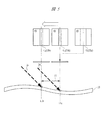
3D検査を半田印刷検査に適用するにあたって、実際の検査対象には基板の反りがあるということと、印刷半田上面と基板面(レジスト面)とでは、スリット光が当った部分のエリア画像上での明度値で最大で100対1位の大きな差があるという難しい問題がある。
たとえば、これまでの技術では、3D検査用データを作成するにあたって、作業者による高さ測定基準点の設定という作業が不可欠であった。すなわち、クリーム半田印刷後の基板上面は、クリーム半田、金あるいは銅あるいは半田コートパッド(印刷半田に隠れてほとんど露出していないパッド)、基材の上を直接覆うレジスト、配線パターン上を覆うレジストなどから構成されている。
3D検査装置は、通常、検査対象を2D撮像する手段を持たないので、作業者に対して目視確認に必要な対象物の拡大画像を提供することができない。これに対して、2D検査と3D検査の共用機では、3D検査で不良と判定した部分の2D拡大画像を、作業者に対して提供することができる。ただし、2D・3D共用機でも、最初に2D検査を実施し、次に3D検査を実施するというシーケンスでは実現が大変難しくなる。
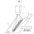
本発明による検査装置は、測定対象物に対して斜め上方からスリット光を照射し、その状況を測定対象物真上に設置したエリアカメラ(CMOSトランジスタ、MOSトランジスタ、CCDなどの撮像素子がアレイ状に配置され、このアレイ状に配置された撮像素子でエリア状に測定対象物を撮すカメラ。言うまでもないことであるが、結果的に2次元画像を取得可能なカメラであれば、エリアカメラに限らず、その他のカメラであってもかまわない)で撮像することにより、測定対象物の高さおよび体積を測定する方式である。
分解能20μm/画素で20.48mm×20.48mmの領域の高さ・体積測定を行う場合、1024画素×32〜256画素の長方形画像を1024枚撮像することになる。
半田印刷検査装置において、2D測定系と3D測定系の2種類の測定系を実装する。この測定系は全く独立した構成でも構わないが、検査装置全体のコストを考えた場合、可能な限り共有できる構造が望ましい。3D検査用データも、2D検査用データと同様、メタルマスクのガーバデータから生成することができる。
先に指定パッド部の3D検査を実行し、その結果を検査結果格納エリアに記録する。その後、全パッドの2D検査を実行する。2D検査で不良と判定したパッドについては、各種測定結果とともに2Dカメラで撮像した画像も記録する。さらには、2D撮像画像を表示装置の指定場所に表示する。
10a,10b,10c,10x 印刷半田
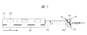
11 高さ測定領域
11a,11b 高さ測定基準ライン
12 基板基材
13 配線パターン
13a スルーホール
14 レジスト
15 パッド部
15a,15b,15c パッド
16 内層パターン部
17 高さ測定基準面
18a,18b,18c パッド上面高さ
20 照明装置
21 赤緑色LED照明装置(2D検査用)
22 青LED照明装置(2D検査用)
23,23a,23b スリット照明装置(3D検査用)
24 スリット光(3D検査用)
241 スリット光跡(基板上)
242 スリット光跡(印刷半田上)
31 カメラ
31a CCDカメラ(2D検査用)
31b CMOSカメラ(3D検査用)
32,32a,32b レンズ
40 撮像範囲(2D検査用)
41 撮像範囲(3D検査用)
50 画像入力記憶部
51 半田撮像画像データ(2D検査用)
52 パッド撮像画像データ(2D検査用)
53 撮像画像データ(3D検査用)
53a 撮像画像データ(基板高さ測定用)
53b 撮像画像データ(印刷半田高さ測定用)
53c,53d,53e 実画像データ(印刷半田高さ測定用)
531 スリット光跡(基板上)
532 スリット光跡(印刷半田上)
533 計測基準ライン
60 画像処理部
61 3D測定データ
62 立体表示(3D測定データ)
71 X軸ロボット
72 Y軸ロボット
73 ロボット制御部
74 表示装置
741 不良パッド拡大表示領域
742 カメラ撮像画像領域
743 基板全体イメージ図および不良パッド表示領域
744 検査カウンタおよび各種情報表示領域
80 全体制御部
81 パッドデータ
82 視野割付データ
83 撮像データ記憶領域
84 検査データ作成プログラム
85 検査実行プログラム
90 QFP
90a 端子
91 コネクタ
91a 端子
91b コネクタ搭載部
92 BGA(CSP)
92a 端子
92b BGA(CSP)搭載部
93a,93b,93c,93d,93e,93f エリア
94a,94b,94c,94d,94e 搭載部
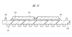
100 基板
100a 多面取り基板
101 ウエハチップ
102 チップ部品
103 半田ボール
104 半田バンプ
105 アンダーフィル
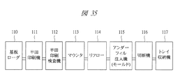
110 基板ローダ
111 半田印刷機
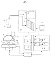
112 半田印刷検査機
113 マウンタ
114 リフロー
115 アンダーフィル注入機
116 切断機
117 トレイ収納機
Claims (4)
- 以下の工程を含む半導体集積回路装置の製造方法:
(a)配線基板上に半田を印刷する工程;
(b)前記配線基板上に印刷された半田を検査する工程;
(c)前記配線基板上に印刷された半田上に回路部品を搭載する工程、
前記(b)工程は、3次元検査と2次元検査を含み、前記3次元検査と前記2次元検査とは、光源の切り替えが可能な共通のカメラを用いて実行され、前記3次元検査と前記2次元検査との間で異なる光の照射を可能とすることにより、前記共通のカメラによって撮像された画像を用いて前記半田の検査を行う。 - 請求項1に記載の半導体集積回路装置の製造方法において、
前記2次元検査は、前記3次元検査の後に実行される。 - 請求項2に記載の半導体集積回路装置の製造方法において、
前記共通のカメラは、CMOSエリアカメラである。 - 請求項2に記載の半導体集積回路装置の製造方法において、
前記光源はLED照明ランプである。
Priority Applications (1)
| Application Number | Priority Date | Filing Date | Title |
|---|---|---|---|
| JP2009250101A JP4892602B2 (ja) | 2009-10-30 | 2009-10-30 | 半導体集積回路装置の製造方法 |
Applications Claiming Priority (1)
| Application Number | Priority Date | Filing Date | Title |
|---|---|---|---|
| JP2009250101A JP4892602B2 (ja) | 2009-10-30 | 2009-10-30 | 半導体集積回路装置の製造方法 |
Related Parent Applications (1)
| Application Number | Title | Priority Date | Filing Date |
|---|---|---|---|
| JP2004015718A Division JP4746841B2 (ja) | 2004-01-23 | 2004-01-23 | 半導体集積回路装置の製造方法 |
Publications (2)
| Publication Number | Publication Date |
|---|---|
| JP2010033593A true JP2010033593A (ja) | 2010-02-12 |
| JP4892602B2 JP4892602B2 (ja) | 2012-03-07 |
Family
ID=41737897
Family Applications (1)
| Application Number | Title | Priority Date | Filing Date |
|---|---|---|---|
| JP2009250101A Expired - Fee Related JP4892602B2 (ja) | 2009-10-30 | 2009-10-30 | 半導体集積回路装置の製造方法 |
Country Status (1)
| Country | Link |
|---|---|
| JP (1) | JP4892602B2 (ja) |
Cited By (3)
| Publication number | Priority date | Publication date | Assignee | Title |
|---|---|---|---|---|
| JP2012177611A (ja) * | 2011-02-25 | 2012-09-13 | Omron Corp | 三次元形状計測装置、および三次元形状計測方法 |
| WO2014093730A1 (en) * | 2012-12-14 | 2014-06-19 | Kla-Tencor Corporation | Apparatus and method for optical inspection, magnetic field and height mapping |
| CN113614205A (zh) * | 2019-03-26 | 2021-11-05 | 杰富意钢铁株式会社 | 炼焦炉砌炉时的检查装置、检查方法以及炼焦炉砌炉方法 |
Families Citing this family (1)
| Publication number | Priority date | Publication date | Assignee | Title |
|---|---|---|---|---|
| TWI784629B (zh) * | 2021-07-21 | 2022-11-21 | 閎康科技股份有限公司 | 焊接品質檢測方法及焊接品質檢測設備 |
Citations (22)
| Publication number | Priority date | Publication date | Assignee | Title |
|---|---|---|---|---|
| JPH05296745A (ja) * | 1992-04-22 | 1993-11-09 | Toshiba Corp | 形状測定装置 |
| JPH07307599A (ja) * | 1994-05-10 | 1995-11-21 | Shigeki Kobayashi | 検査装置及び製品製造方法 |
| JPH07311025A (ja) * | 1994-05-17 | 1995-11-28 | Komatsu Ltd | 3次元形状検査装置 |
| JPH08327332A (ja) * | 1995-05-30 | 1996-12-13 | Ando Electric Co Ltd | クリームはんだ膜厚測定装置 |
| JPH11198343A (ja) * | 1998-01-16 | 1999-07-27 | Furukawa Electric Co Ltd:The | クリーム半田印刷検査方法 |
| JPH11241916A (ja) * | 1998-02-25 | 1999-09-07 | Juki Corp | 高さ測定方法、高さデータ処理方法及び高さ測定装置 |
| WO1999056075A1 (en) * | 1998-04-28 | 1999-11-04 | Semiconductor Technologies & Instruments, Inc. | Inspection system and method for leads of semiconductor devices |
| JP2000022326A (ja) * | 1998-07-07 | 2000-01-21 | Sankyo Seiki Mfg Co Ltd | はんだ検査装置及び方法 |
| JP2000131037A (ja) * | 1998-10-26 | 2000-05-12 | Hitachi Denshi Ltd | 物体形状検査装置 |
| JP2000193432A (ja) * | 1998-12-25 | 2000-07-14 | Tani Denki Kogyo Kk | 画像認識による計測方法および装置 |
| US6118540A (en) * | 1997-07-11 | 2000-09-12 | Semiconductor Technologies & Instruments, Inc. | Method and apparatus for inspecting a workpiece |
| JP2000337823A (ja) * | 1999-05-27 | 2000-12-08 | Mitsubishi Heavy Ind Ltd | 表面検査装置及び表面検査方法 |
| JP2001130728A (ja) * | 1999-11-04 | 2001-05-15 | Anritsu Corp | プリント基板の搬送装置及び方法並びにプリント基板検査装置 |
| JP2001153629A (ja) * | 1999-11-29 | 2001-06-08 | Anritsu Corp | 印刷半田測定装置 |
| JP3203397B2 (ja) * | 1992-08-25 | 2001-08-27 | 松下電器産業株式会社 | はんだ付け状態検査装置とはんだ付け状態検査方法 |
| JP2003121115A (ja) * | 2001-10-16 | 2003-04-23 | Nikke Kikai Seisakusho:Kk | 外観検査装置および外観検査方法 |
| JP2003279334A (ja) * | 2002-02-01 | 2003-10-02 | Ckd Corp | 三次元計測装置、フィルタ格子縞板及び照明手段 |
| US20040184653A1 (en) * | 2003-03-20 | 2004-09-23 | Baer Richard L. | Optical inspection system, illumination apparatus and method for use in imaging specular objects based on illumination gradients |
| JP2004317291A (ja) * | 2003-04-16 | 2004-11-11 | Ckd Corp | 半田外観検査装置 |
| JP2004317126A (ja) * | 2003-04-10 | 2004-11-11 | Renesas Technology Corp | はんだ印刷装置 |
| JP2005207918A (ja) * | 2004-01-23 | 2005-08-04 | Renesas Technology Corp | 半導体集積回路装置の製造方法 |
| JP2006527372A (ja) * | 2003-06-11 | 2006-11-30 | ソルヴィジョン | 感度及びダイナミックレンジを増大させた3d及び2d測定システム及びその方法 |
-
2009
- 2009-10-30 JP JP2009250101A patent/JP4892602B2/ja not_active Expired - Fee Related
Patent Citations (24)
| Publication number | Priority date | Publication date | Assignee | Title |
|---|---|---|---|---|
| JPH05296745A (ja) * | 1992-04-22 | 1993-11-09 | Toshiba Corp | 形状測定装置 |
| JP3203397B2 (ja) * | 1992-08-25 | 2001-08-27 | 松下電器産業株式会社 | はんだ付け状態検査装置とはんだ付け状態検査方法 |
| JPH07307599A (ja) * | 1994-05-10 | 1995-11-21 | Shigeki Kobayashi | 検査装置及び製品製造方法 |
| JPH07311025A (ja) * | 1994-05-17 | 1995-11-28 | Komatsu Ltd | 3次元形状検査装置 |
| JPH08327332A (ja) * | 1995-05-30 | 1996-12-13 | Ando Electric Co Ltd | クリームはんだ膜厚測定装置 |
| US6118540A (en) * | 1997-07-11 | 2000-09-12 | Semiconductor Technologies & Instruments, Inc. | Method and apparatus for inspecting a workpiece |
| JPH11198343A (ja) * | 1998-01-16 | 1999-07-27 | Furukawa Electric Co Ltd:The | クリーム半田印刷検査方法 |
| JPH11241916A (ja) * | 1998-02-25 | 1999-09-07 | Juki Corp | 高さ測定方法、高さデータ処理方法及び高さ測定装置 |
| WO1999056075A1 (en) * | 1998-04-28 | 1999-11-04 | Semiconductor Technologies & Instruments, Inc. | Inspection system and method for leads of semiconductor devices |
| JP2002513137A (ja) * | 1998-04-28 | 2002-05-08 | セミコンダクター テクノロジーズ アンド インスツルメンツ, インコーポレイテッド | 半導体デバイスのリードの検査装置及び方法 |
| JP2000022326A (ja) * | 1998-07-07 | 2000-01-21 | Sankyo Seiki Mfg Co Ltd | はんだ検査装置及び方法 |
| JP2000131037A (ja) * | 1998-10-26 | 2000-05-12 | Hitachi Denshi Ltd | 物体形状検査装置 |
| JP2000193432A (ja) * | 1998-12-25 | 2000-07-14 | Tani Denki Kogyo Kk | 画像認識による計測方法および装置 |
| JP2000337823A (ja) * | 1999-05-27 | 2000-12-08 | Mitsubishi Heavy Ind Ltd | 表面検査装置及び表面検査方法 |
| JP2001130728A (ja) * | 1999-11-04 | 2001-05-15 | Anritsu Corp | プリント基板の搬送装置及び方法並びにプリント基板検査装置 |
| JP2001153629A (ja) * | 1999-11-29 | 2001-06-08 | Anritsu Corp | 印刷半田測定装置 |
| JP2003121115A (ja) * | 2001-10-16 | 2003-04-23 | Nikke Kikai Seisakusho:Kk | 外観検査装置および外観検査方法 |
| JP2003279334A (ja) * | 2002-02-01 | 2003-10-02 | Ckd Corp | 三次元計測装置、フィルタ格子縞板及び照明手段 |
| US20040184653A1 (en) * | 2003-03-20 | 2004-09-23 | Baer Richard L. | Optical inspection system, illumination apparatus and method for use in imaging specular objects based on illumination gradients |
| WO2004086015A2 (en) * | 2003-03-20 | 2004-10-07 | Agilent Technologies, Inc. | Optical inspection system, illumination apparatus and method for imaging specular objects based on illumination gradients |
| JP2004317126A (ja) * | 2003-04-10 | 2004-11-11 | Renesas Technology Corp | はんだ印刷装置 |
| JP2004317291A (ja) * | 2003-04-16 | 2004-11-11 | Ckd Corp | 半田外観検査装置 |
| JP2006527372A (ja) * | 2003-06-11 | 2006-11-30 | ソルヴィジョン | 感度及びダイナミックレンジを増大させた3d及び2d測定システム及びその方法 |
| JP2005207918A (ja) * | 2004-01-23 | 2005-08-04 | Renesas Technology Corp | 半導体集積回路装置の製造方法 |
Cited By (4)
| Publication number | Priority date | Publication date | Assignee | Title |
|---|---|---|---|---|
| JP2012177611A (ja) * | 2011-02-25 | 2012-09-13 | Omron Corp | 三次元形状計測装置、および三次元形状計測方法 |
| WO2014093730A1 (en) * | 2012-12-14 | 2014-06-19 | Kla-Tencor Corporation | Apparatus and method for optical inspection, magnetic field and height mapping |
| US9513230B2 (en) | 2012-12-14 | 2016-12-06 | Kla-Tencor Corporation | Apparatus and method for optical inspection, magnetic field and height mapping |
| CN113614205A (zh) * | 2019-03-26 | 2021-11-05 | 杰富意钢铁株式会社 | 炼焦炉砌炉时的检查装置、检查方法以及炼焦炉砌炉方法 |
Also Published As
| Publication number | Publication date |
|---|---|
| JP4892602B2 (ja) | 2012-03-07 |
Similar Documents
| Publication | Publication Date | Title |
|---|---|---|
| JP4746841B2 (ja) | 半導体集積回路装置の製造方法 | |
| JP5421763B2 (ja) | 検査装置および検査方法 | |
| JP4493421B2 (ja) | プリント回路基板検査装置とプリント回路基板組み立て検査ラインシステムおよびプログラム | |
| KR100915128B1 (ko) | 부품장착 관리방법, 장착검사장치 및 장착시스템 | |
| US9250198B2 (en) | Board inspection apparatus | |
| TWI858453B (zh) | 半導體製造裝置、檢查裝置及半導體裝置的製造方法 | |
| JP4892602B2 (ja) | 半導体集積回路装置の製造方法 | |
| TWI452284B (zh) | The method of detecting the mark of the multi-board, the method of detecting the device and the multi-board | |
| JP3722608B2 (ja) | 外観検査装置 | |
| CN105845594A (zh) | 检查半导体封装的印刷电路板的方法 | |
| JP6387620B2 (ja) | 品質管理システム | |
| JP4734650B2 (ja) | クリームはんだ印刷の不良検出方法および装置 | |
| JP3868917B2 (ja) | 三次元計測装置及び検査装置 | |
| JP2006286744A (ja) | 半導体実装基板、半導体実装用基板、その外観検査方法及び外観検査装置 | |
| TWI784051B (zh) | 半導體材料附接方法 | |
| JPH0315707A (ja) | リード検査方法およびそれに使用されるリード測定装置並びにリード検査装置 | |
| JP2008041758A (ja) | フラックスの転写状態検査方法及び装置 | |
| CN109616427B (zh) | 半导体材料附接方法 | |
| JP2025073834A (ja) | フラックス塗布状態検査装置及びフラックス塗布状態検査方法 | |
| CN105580122A (zh) | 用于定位具有电子元器件的承载件的方法和以此类方法生产的电子元器件 | |
| JPH09330954A (ja) | パッケージ搭載位置確認装置 | |
| JPH0213838A (ja) | リード検査方法およびそれに使用されるリード測定装置並びにリード検査装置 | |
| KR20100052361A (ko) | 표면실장모듈 검사 시스템 |
Legal Events
| Date | Code | Title | Description |
|---|---|---|---|
| A711 | Notification of change in applicant |
Free format text: JAPANESE INTERMEDIATE CODE: A712 Effective date: 20100528 |
|
| A131 | Notification of reasons for refusal |
Free format text: JAPANESE INTERMEDIATE CODE: A131 Effective date: 20110222 |
|
| A521 | Written amendment |
Free format text: JAPANESE INTERMEDIATE CODE: A523 Effective date: 20110420 |
|
| A131 | Notification of reasons for refusal |
Free format text: JAPANESE INTERMEDIATE CODE: A131 Effective date: 20110517 |
|
| A521 | Written amendment |
Free format text: JAPANESE INTERMEDIATE CODE: A523 Effective date: 20110714 |
|
| A131 | Notification of reasons for refusal |
Free format text: JAPANESE INTERMEDIATE CODE: A131 Effective date: 20110802 |
|
| A521 | Written amendment |
Free format text: JAPANESE INTERMEDIATE CODE: A523 Effective date: 20110930 |
|
| TRDD | Decision of grant or rejection written | ||
| A01 | Written decision to grant a patent or to grant a registration (utility model) |
Free format text: JAPANESE INTERMEDIATE CODE: A01 Effective date: 20111122 |
|
| A01 | Written decision to grant a patent or to grant a registration (utility model) |
Free format text: JAPANESE INTERMEDIATE CODE: A01 |
|
| A61 | First payment of annual fees (during grant procedure) |
Free format text: JAPANESE INTERMEDIATE CODE: A61 Effective date: 20111219 |
|
| R150 | Certificate of patent or registration of utility model |
Ref document number: 4892602 Country of ref document: JP Free format text: JAPANESE INTERMEDIATE CODE: R150 Free format text: JAPANESE INTERMEDIATE CODE: R150 |
|
| FPAY | Renewal fee payment (event date is renewal date of database) |
Free format text: PAYMENT UNTIL: 20141222 Year of fee payment: 3 |
|
| S531 | Written request for registration of change of domicile |
Free format text: JAPANESE INTERMEDIATE CODE: R313531 |
|
| R350 | Written notification of registration of transfer |
Free format text: JAPANESE INTERMEDIATE CODE: R350 |
|
| LAPS | Cancellation because of no payment of annual fees |