JP2010021229A - 半導体装置 - Google Patents
半導体装置 Download PDFInfo
- Publication number
- JP2010021229A JP2010021229A JP2008178768A JP2008178768A JP2010021229A JP 2010021229 A JP2010021229 A JP 2010021229A JP 2008178768 A JP2008178768 A JP 2008178768A JP 2008178768 A JP2008178768 A JP 2008178768A JP 2010021229 A JP2010021229 A JP 2010021229A
- Authority
- JP
- Japan
- Prior art keywords
- region
- active region
- mis transistor
- semiconductor device
- gate electrode
- Prior art date
- Legal status (The legal status is an assumption and is not a legal conclusion. Google has not performed a legal analysis and makes no representation as to the accuracy of the status listed.)
- Granted
Links
Images


Classifications
-
- H—ELECTRICITY
- H10—SEMICONDUCTOR DEVICES; ELECTRIC SOLID-STATE DEVICES NOT OTHERWISE PROVIDED FOR
- H10D—INORGANIC ELECTRIC SEMICONDUCTOR DEVICES
- H10D30/00—Field-effect transistors [FET]
- H10D30/60—Insulated-gate field-effect transistors [IGFET]
- H10D30/601—Insulated-gate field-effect transistors [IGFET] having lightly-doped drain or source extensions, e.g. LDD IGFETs or DDD IGFETs
-
- H—ELECTRICITY
- H10—SEMICONDUCTOR DEVICES; ELECTRIC SOLID-STATE DEVICES NOT OTHERWISE PROVIDED FOR
- H10D—INORGANIC ELECTRIC SEMICONDUCTOR DEVICES
- H10D30/00—Field-effect transistors [FET]
- H10D30/60—Insulated-gate field-effect transistors [IGFET]
- H10D30/791—Arrangements for exerting mechanical stress on the crystal lattice of the channel regions
- H10D30/797—Arrangements for exerting mechanical stress on the crystal lattice of the channel regions being in source or drain regions, e.g. SiGe source or drain
-
- H—ELECTRICITY
- H10—SEMICONDUCTOR DEVICES; ELECTRIC SOLID-STATE DEVICES NOT OTHERWISE PROVIDED FOR
- H10D—INORGANIC ELECTRIC SEMICONDUCTOR DEVICES
- H10D84/00—Integrated devices formed in or on semiconductor substrates that comprise only semiconducting layers, e.g. on Si wafers or on GaAs-on-Si wafers
- H10D84/01—Manufacture or treatment
- H10D84/0123—Integrating together multiple components covered by H10D12/00 or H10D30/00, e.g. integrating multiple IGBTs
- H10D84/0126—Integrating together multiple components covered by H10D12/00 or H10D30/00, e.g. integrating multiple IGBTs the components including insulated gates, e.g. IGFETs
- H10D84/013—Manufacturing their source or drain regions, e.g. silicided source or drain regions
- H10D84/0133—Manufacturing common source or drain regions between multiple IGFETs
-
- H—ELECTRICITY
- H10—SEMICONDUCTOR DEVICES; ELECTRIC SOLID-STATE DEVICES NOT OTHERWISE PROVIDED FOR
- H10D—INORGANIC ELECTRIC SEMICONDUCTOR DEVICES
- H10D84/00—Integrated devices formed in or on semiconductor substrates that comprise only semiconducting layers, e.g. on Si wafers or on GaAs-on-Si wafers
- H10D84/01—Manufacture or treatment
- H10D84/0123—Integrating together multiple components covered by H10D12/00 or H10D30/00, e.g. integrating multiple IGBTs
- H10D84/0126—Integrating together multiple components covered by H10D12/00 or H10D30/00, e.g. integrating multiple IGBTs the components including insulated gates, e.g. IGFETs
- H10D84/0165—Integrating together multiple components covered by H10D12/00 or H10D30/00, e.g. integrating multiple IGBTs the components including insulated gates, e.g. IGFETs the components including complementary IGFETs, e.g. CMOS devices
- H10D84/0167—Manufacturing their channels
-
- H—ELECTRICITY
- H10—SEMICONDUCTOR DEVICES; ELECTRIC SOLID-STATE DEVICES NOT OTHERWISE PROVIDED FOR
- H10D—INORGANIC ELECTRIC SEMICONDUCTOR DEVICES
- H10D84/00—Integrated devices formed in or on semiconductor substrates that comprise only semiconducting layers, e.g. on Si wafers or on GaAs-on-Si wafers
- H10D84/01—Manufacture or treatment
- H10D84/0123—Integrating together multiple components covered by H10D12/00 or H10D30/00, e.g. integrating multiple IGBTs
- H10D84/0126—Integrating together multiple components covered by H10D12/00 or H10D30/00, e.g. integrating multiple IGBTs the components including insulated gates, e.g. IGFETs
- H10D84/0165—Integrating together multiple components covered by H10D12/00 or H10D30/00, e.g. integrating multiple IGBTs the components including insulated gates, e.g. IGFETs the components including complementary IGFETs, e.g. CMOS devices
- H10D84/017—Manufacturing their source or drain regions, e.g. silicided source or drain regions
-
- H—ELECTRICITY
- H10—SEMICONDUCTOR DEVICES; ELECTRIC SOLID-STATE DEVICES NOT OTHERWISE PROVIDED FOR
- H10D—INORGANIC ELECTRIC SEMICONDUCTOR DEVICES
- H10D84/00—Integrated devices formed in or on semiconductor substrates that comprise only semiconducting layers, e.g. on Si wafers or on GaAs-on-Si wafers
- H10D84/01—Manufacture or treatment
- H10D84/0123—Integrating together multiple components covered by H10D12/00 or H10D30/00, e.g. integrating multiple IGBTs
- H10D84/0126—Integrating together multiple components covered by H10D12/00 or H10D30/00, e.g. integrating multiple IGBTs the components including insulated gates, e.g. IGFETs
- H10D84/0165—Integrating together multiple components covered by H10D12/00 or H10D30/00, e.g. integrating multiple IGBTs the components including insulated gates, e.g. IGFETs the components including complementary IGFETs, e.g. CMOS devices
- H10D84/0188—Manufacturing their isolation regions
-
- H—ELECTRICITY
- H10—SEMICONDUCTOR DEVICES; ELECTRIC SOLID-STATE DEVICES NOT OTHERWISE PROVIDED FOR
- H10D—INORGANIC ELECTRIC SEMICONDUCTOR DEVICES
- H10D84/00—Integrated devices formed in or on semiconductor substrates that comprise only semiconducting layers, e.g. on Si wafers or on GaAs-on-Si wafers
- H10D84/01—Manufacture or treatment
- H10D84/02—Manufacture or treatment characterised by using material-based technologies
- H10D84/03—Manufacture or treatment characterised by using material-based technologies using Group IV technology, e.g. silicon technology or silicon-carbide [SiC] technology
- H10D84/038—Manufacture or treatment characterised by using material-based technologies using Group IV technology, e.g. silicon technology or silicon-carbide [SiC] technology using silicon technology, e.g. SiGe
-
- H—ELECTRICITY
- H10—SEMICONDUCTOR DEVICES; ELECTRIC SOLID-STATE DEVICES NOT OTHERWISE PROVIDED FOR
- H10D—INORGANIC ELECTRIC SEMICONDUCTOR DEVICES
- H10D84/00—Integrated devices formed in or on semiconductor substrates that comprise only semiconducting layers, e.g. on Si wafers or on GaAs-on-Si wafers
- H10D84/80—Integrated devices formed in or on semiconductor substrates that comprise only semiconducting layers, e.g. on Si wafers or on GaAs-on-Si wafers characterised by the integration of at least one component covered by groups H10D12/00 or H10D30/00, e.g. integration of IGFETs
- H10D84/82—Integrated devices formed in or on semiconductor substrates that comprise only semiconducting layers, e.g. on Si wafers or on GaAs-on-Si wafers characterised by the integration of at least one component covered by groups H10D12/00 or H10D30/00, e.g. integration of IGFETs of only field-effect components
- H10D84/83—Integrated devices formed in or on semiconductor substrates that comprise only semiconducting layers, e.g. on Si wafers or on GaAs-on-Si wafers characterised by the integration of at least one component covered by groups H10D12/00 or H10D30/00, e.g. integration of IGFETs of only field-effect components of only insulated-gate FETs [IGFET]
- H10D84/8311—Integrated devices formed in or on semiconductor substrates that comprise only semiconducting layers, e.g. on Si wafers or on GaAs-on-Si wafers characterised by the integration of at least one component covered by groups H10D12/00 or H10D30/00, e.g. integration of IGFETs of only field-effect components of only insulated-gate FETs [IGFET] the IGFETs characterised by having different channel structures
-
- H—ELECTRICITY
- H10—SEMICONDUCTOR DEVICES; ELECTRIC SOLID-STATE DEVICES NOT OTHERWISE PROVIDED FOR
- H10D—INORGANIC ELECTRIC SEMICONDUCTOR DEVICES
- H10D84/00—Integrated devices formed in or on semiconductor substrates that comprise only semiconducting layers, e.g. on Si wafers or on GaAs-on-Si wafers
- H10D84/80—Integrated devices formed in or on semiconductor substrates that comprise only semiconducting layers, e.g. on Si wafers or on GaAs-on-Si wafers characterised by the integration of at least one component covered by groups H10D12/00 or H10D30/00, e.g. integration of IGFETs
- H10D84/82—Integrated devices formed in or on semiconductor substrates that comprise only semiconducting layers, e.g. on Si wafers or on GaAs-on-Si wafers characterised by the integration of at least one component covered by groups H10D12/00 or H10D30/00, e.g. integration of IGFETs of only field-effect components
- H10D84/83—Integrated devices formed in or on semiconductor substrates that comprise only semiconducting layers, e.g. on Si wafers or on GaAs-on-Si wafers characterised by the integration of at least one component covered by groups H10D12/00 or H10D30/00, e.g. integration of IGFETs of only field-effect components of only insulated-gate FETs [IGFET]
- H10D84/85—Complementary IGFETs, e.g. CMOS
-
- H—ELECTRICITY
- H10—SEMICONDUCTOR DEVICES; ELECTRIC SOLID-STATE DEVICES NOT OTHERWISE PROVIDED FOR
- H10D—INORGANIC ELECTRIC SEMICONDUCTOR DEVICES
- H10D30/00—Field-effect transistors [FET]
- H10D30/01—Manufacture or treatment
- H10D30/021—Manufacture or treatment of FETs having insulated gates [IGFET]
- H10D30/0212—Manufacture or treatment of FETs having insulated gates [IGFET] using self-aligned silicidation
-
- H—ELECTRICITY
- H10—SEMICONDUCTOR DEVICES; ELECTRIC SOLID-STATE DEVICES NOT OTHERWISE PROVIDED FOR
- H10D—INORGANIC ELECTRIC SEMICONDUCTOR DEVICES
- H10D62/00—Semiconductor bodies, or regions thereof, of devices having potential barriers
- H10D62/80—Semiconductor bodies, or regions thereof, of devices having potential barriers characterised by the materials
- H10D62/82—Heterojunctions
- H10D62/822—Heterojunctions comprising only Group IV materials heterojunctions, e.g. Si/Ge heterojunctions
Landscapes
- Metal-Oxide And Bipolar Metal-Oxide Semiconductor Integrated Circuits (AREA)
- Design And Manufacture Of Integrated Circuits (AREA)
- Insulated Gate Type Field-Effect Transistor (AREA)
- Element Separation (AREA)
- Semiconductor Integrated Circuits (AREA)
Abstract
【解決手段】半導体装置は、第1のウエル領域3a及び第2のウエル領域3bと、素子分離領域2に囲まれた第1の活性領域21aと、素子分離領域2、2Bに囲まれた第2の活性領域21bと、第1の活性領域21a上に形成され、凹部内に埋め込まれたSi混晶層からなるソース/ドレイン領域を有する第2導電型の第1のMISトランジスタMP2と、第2の活性領域21b上に形成された第1導電型の第2のMISトランジスタMN2と、第1の活性領域21a上に形成された第2導電型の分離用MISトランジスタDP2とを備える。第1のMISトランジスタのソース/ドレイン領域は、第1の活性領域21aにおけるゲート長方向の端部に位置する素子分離領域2に接していない。
【選択図】図1
Description
)。また、図7(a)、(b)は、図6に示すVIIa-VIIa線、およびVIIb-VIIb線における従来の半導体装置の断面図である。
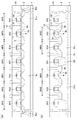
図1は、本発明の第1の実施形態に係る半導体装置において、2入力NANDゲート(左側)と2入力NORゲート(右側)とをMISトランジスタのゲート長方向(図中の左右方向)に隣接させたレイアウト図である。また、図2(a)、(b)は、図1に示すIIa-IIa線、およびIIb-IIb線における第1の実施形態に係る半導体装置の断面図である。ここで、2入力NANDゲートと2入力NORゲートの回路構成は図5(a)、(b)に示す通りである。
次に、活性領域21aを含むN型ウエル領域3a上をマスクで覆った状態で、活性領域21b、21cのうち各ゲート配線およびサイドウォールスペーサ7の外側方に位置する領域にN型不純物をイオン注入してN型ソース/ドレイン領域8bを形成する。なお、P型ソース/ドレイン領域8aとN型ソース/ドレイン領域8bとはどちらを先に形成してもよい。
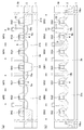
図3は、本発明の第2の実施形態に係る半導体装置において、2入力NANDゲート(左側)と2入力NORゲート(右側)とをMISトランジスタのゲート長方向(図中の左右方向)に隣接させたレイアウト図である。また、図4(a)、(b)は、図3に示すIVa-IVa線、およびIVb-IVb線における第2の実施形態に係る半導体装置の断面図である。本実施形態の半導体装置は、N型MISトランジスタのN型ソース/ドレイン領域をSiC層で構成し、隣接する2つのN型MISトランジスタ間の電気的分離のためにゲート分離方式を採用したものである。以下の説明において、第1の実施形態と同様の箇所には同一の符号を付し、その説明を省略または簡略化する。
2、2A、2B 素子分離領域
3a N型ウエル領域
3b P型ウエル領域
4 ゲート絶縁膜
6a P型エクステンション領域
6b N型エクステンション領域
7 サイドウォールスペーサ
8a、18a P型ソース/ドレイン領域
8ax P型ソース/ドレイン領域
8b、18b N型ソース/ドレイン領域
18bx N型ソース/ドレイン領域
9 ソース/ドレイン上シリサイド層
10 層間絶縁膜
11 コンタクトプラグ
12 金属配線
21a、31a、31b 活性領域
21b、21c、31c 活性領域
21d、31d N型基板コンタクト領域
21e、31e P型基板コンタクト領域
30 ゲート上シリサイド層
5G1、5G2、5G3、5G4 ゲート配線
5N1、5N2、5N3 分離用ゲート配線
5P1、5P2、5P3 分離用ゲート配線
DN1、DN2、DN3 分離用MISトランジスタ
DP1、DP2、DP3 分離用MISトランジスタ
MN1、MN2、MN3、MN4 N型MISトランジスタ
MP1、MP2、MP3、MP4 P型MISトランジスタ
Claims (14)
- 共に半導体基板内に形成され、ゲート幅方向に隣接する第1導電型の第1のウエル領域および第2導電型の第2のウエル領域と、
前記第1のウエル領域内に形成された素子分離領域に囲まれた前記半導体基板からなる第1の活性領域と、
前記第2のウエル領域内に形成された前記素子分離領域に囲まれた前記半導体基板からなる第2の活性領域と、
前記第1の活性領域上に形成された第1のゲート電極と、前記第1の活性領域における前記第1のゲート電極の側方下の領域に設けられた凹部内に埋め込まれた第1のSi混晶層からなる第2導電型の第1のソース/ドレイン領域とを有する第2導電型の第1のMISトランジスタと、
前記第2の活性領域上に形成された第2のゲート電極と、前記第2の活性領域における前記第2のゲート電極の側方下の領域に形成された第1導電型の第2のソース/ドレイン領域を有する第1導電型の第2のMISトランジスタと、
前記第1の活性領域上に形成され、前記第1のウエル領域と同電位に接続された第1の分離用ゲート電極を有する第2導電型の第1の分離用MISトランジスタとを備え、
前記第2の活性領域には、分離用MISトランジスタは形成されておらず、
前記第1のMISトランジスタの前記第1のソース/ドレイン領域は、前記第1の活性領域におけるゲート長方向の端部に位置する前記素子分離領域には接していないことを特徴とする半導体装置。 - 請求項1に記載の半導体装置において、
前記第1のMISトランジスタの前記第1のゲート電極と前記第2のMISトランジスタの前記第2のゲート電極とを含む第1のゲート配線は、前記第1の活性領域上から前記第2の活性領域上に亘って形成されていることを特徴とする半導体装置。 - 請求項1又は2に記載の半導体装置において、
前記第1のウエル領域内に、前記第1の活性領域から見てゲート幅方向に前記素子分離領域を挟んで設けられ、前記第2のウエル領域との間で前記第1の活性領域を挟む位置に形成された第1導電型の第1の基板コンタクト領域と、
前記第2のウエル領域内に、前記第2の活性領域から見てゲート幅方向に前記素子分離領域を挟んで設けられ、前記第1のウエル領域との間で前記第2の活性領域を挟む位置に形成された第2導電型の第2の基板コンタクト領域とをさらに備え、
前記第1の分離用MISトランジスタの第1の分離用ゲート電極を含む第1の分離用ゲート配線は、少なくとも前記第1の活性領域を跨いで前記第1の基板コンタクト領域上にまで延びており、前記第1の基板コンタクト領域と同電位に接続されていることを特徴とする半導体装置。 - 請求項3に記載の半導体装置において、
前記第1の分離用ゲート配線は、前記第2の活性領域の側方に位置する前記素子分離領域上まで延びていることを特徴とする半導体装置。 - 請求項1〜4のうちいずれか1項に記載の半導体装置において、
前記第1の活性領域における前記第1の分離用ゲート電極の一側方下の領域には、前記第1のSi混晶層が形成されており、
前記第1の活性領域における前記第1の分離用ゲート電極の他側方下の領域には、前記第1の活性領域に設けられた凹部内に埋め込まれ、前記第1の活性領域におけるゲート長方向の端部に位置する前記素子分離領域に接する第2のSi混晶層が形成されていることを特徴とする半導体装置。 - 請求項5に記載の半導体装置において、
前記第2のSi混晶層は、前記第1の混晶層に比べて上面が凹んでいることを特徴とする半導体装置。 - 請求項1〜6に記載の半導体装置において、
前記第1の活性領域上に形成された第3のゲート電極と、前記第1の活性領域における前記第3のゲート電極の側方下の領域に設けられた凹部内に埋め込まれた前記第1のSi混晶層からなる第2導電型の第3のソース/ドレイン領域とを有する第2導電型の第3のMISトランジスタと、
前記第1の活性領域における前記第1のソース/ドレイン領域と前記第3のソース/ドレイン領域との間に位置する領域上に形成され、前記第1のウエル領域と同電位に接続された第2の分離用ゲート電極を有する第2導電型の第2の分離用MISトランジスタとをさらに備えていることを特徴とする半導体装置。 - 請求項7に記載の半導体装置において、
前記第2のウエル領域内に形成された前記素子分離領域に囲まれ、前記第2の活性領域から見てゲート長方向に前記素子分離領域を挟んで設けられた前記半導体基板からなる第3の活性領域と、
前記第3の活性領域上に形成された第4のゲート電極と、前記第3の活性領域における前記第4のゲート電極の側方下の領域に形成された第1導電型の第4のソース/ドレイン領域を有する第1導電型の第4のMISトランジスタとをさらに備え、
前記第2の分離用ゲート電極は、前記第2の活性領域と前記第3の活性領域との間に位置する前記素子分離領域上まで延びていることを特徴とする半導体装置。 - 請求項8に記載の半導体装置において、
前記第3のMISトランジスタの前記第3のゲート電極と前記第4のMISトランジスタの前記第4のゲート電極とを含む第2のゲート配線は、前記第1の活性領域上から前記第3の活性領域上に亘って形成されていることを特徴とする半導体装置。 - 請求項1〜4に記載の半導体装置において、
前記第1の活性領域上に形成された第3のゲート電極と、前記第1の活性領域における前記第3のゲート電極の側方下の領域に設けられた凹部内に埋め込まれた前記第1のSi混晶層からなる第2導電型の第3のソース/ドレイン領域とを有する第2導電型の第3のMISトランジスタをさらに備え、
前記第1の分離用ゲート電極は、前記第1の活性領域における前記第1のソース/ドレイン領域と前記第3のソース/ドレイン領域との間に位置する領域上に形成されていることを特徴とする半導体装置。 - 請求項9に記載の半導体装置において、
前記第2のウエル領域内に形成された前記素子分離領域に囲まれ、前記第2の活性領域から見てゲート長方向に前記素子分離領域を挟んで設けられた前記半導体基板からなる第3の活性領域と、
前記第3の活性領域上に形成された第4のゲート電極と、前記第3の活性領域における前記第4のゲート電極の側方下の領域に形成された第1導電型の第4のソース/ドレイン領域を有する第1導電型の第4のMISトランジスタとをさらに備えていることを特徴とする半導体装置。 - 請求項11に記載の半導体装置において、
前記第3のMISトランジスタの前記第3のゲート電極と前記第4のMISトランジスタの前記第4のゲート電極とを含む第2のゲート配線は、前記第1の活性領域上から前記第3の活性領域上に亘って形成されていることを特徴とする半導体装置。 - 請求項1〜12に記載の半導体装置において、
前記第1のMISトランジスタはPチャネル型、前記第2のMISトランジスタはNチャネル型であり、
前記第1の分離用ゲート電極は、電源線に接続されており、
前記第1のSi混晶層はSiGeからなることを特徴とする半導体装置。 - 請求項1〜12に記載の半導体装置において、
前記第1のMISトランジスタはNチャネル型、前記第2のMISトランジスタはPチャネル型であり、
前記第1の分離用ゲート電極は、接地線に接続されており、
前記第1のSi混晶層はSiCからなることを特徴とする半導体装置。
Priority Applications (3)
| Application Number | Priority Date | Filing Date | Title |
|---|---|---|---|
| JP2008178768A JP5064321B2 (ja) | 2008-07-09 | 2008-07-09 | 半導体装置 |
| PCT/JP2009/002288 WO2010004680A1 (ja) | 2008-07-09 | 2009-05-25 | 半導体装置 |
| US12/689,723 US8217429B2 (en) | 2008-07-09 | 2010-01-19 | Semiconductor device |
Applications Claiming Priority (1)
| Application Number | Priority Date | Filing Date | Title |
|---|---|---|---|
| JP2008178768A JP5064321B2 (ja) | 2008-07-09 | 2008-07-09 | 半導体装置 |
Publications (2)
| Publication Number | Publication Date |
|---|---|
| JP2010021229A true JP2010021229A (ja) | 2010-01-28 |
| JP5064321B2 JP5064321B2 (ja) | 2012-10-31 |
Family
ID=41506808
Family Applications (1)
| Application Number | Title | Priority Date | Filing Date |
|---|---|---|---|
| JP2008178768A Expired - Fee Related JP5064321B2 (ja) | 2008-07-09 | 2008-07-09 | 半導体装置 |
Country Status (3)
| Country | Link |
|---|---|
| US (1) | US8217429B2 (ja) |
| JP (1) | JP5064321B2 (ja) |
| WO (1) | WO2010004680A1 (ja) |
Cited By (4)
| Publication number | Priority date | Publication date | Assignee | Title |
|---|---|---|---|---|
| JP2011238844A (ja) * | 2010-05-12 | 2011-11-24 | Renesas Electronics Corp | 半導体装置 |
| WO2012004911A1 (ja) * | 2010-07-07 | 2012-01-12 | パナソニック株式会社 | 半導体装置及びその製造方法 |
| JP2012182277A (ja) * | 2011-03-01 | 2012-09-20 | Fujitsu Semiconductor Ltd | 半導体装置 |
| JP2012216776A (ja) * | 2011-03-31 | 2012-11-08 | Sony Corp | 半導体装置、および、その製造方法 |
Families Citing this family (11)
| Publication number | Priority date | Publication date | Assignee | Title |
|---|---|---|---|---|
| GB2466313A (en) * | 2008-12-22 | 2010-06-23 | Cambridge Silicon Radio Ltd | Radio Frequency CMOS Transistor |
| JP6031086B2 (ja) * | 2012-03-08 | 2016-11-24 | 株式会社ソシオネクスト | 半導体集積回路装置 |
| US9024418B2 (en) | 2013-03-14 | 2015-05-05 | Qualcomm Incorporated | Local interconnect structures for high density |
| CN105359275B (zh) | 2013-07-08 | 2019-06-14 | 宜普电源转换公司 | 氮化镓器件和集成电路中的隔离结构 |
| US9318476B2 (en) | 2014-03-03 | 2016-04-19 | Qualcomm Incorporated | High performance standard cell with continuous oxide definition and characterized leakage current |
| US10177133B2 (en) * | 2014-05-16 | 2019-01-08 | Taiwan Semiconductor Manufacturing Co., Ltd. | Semiconductor device including source/drain contact having height below gate stack |
| US10361195B2 (en) * | 2014-09-04 | 2019-07-23 | Samsung Electronics Co., Ltd. | Semiconductor device with an isolation gate and method of forming |
| KR20170024703A (ko) * | 2015-08-26 | 2017-03-08 | 에스케이하이닉스 주식회사 | 드라이버를 포함하는 반도체 장치 |
| US10692808B2 (en) | 2017-09-18 | 2020-06-23 | Qualcomm Incorporated | High performance cell design in a technology with high density metal routing |
| JP7268408B2 (ja) * | 2019-03-06 | 2023-05-08 | ユナイテッド・セミコンダクター・ジャパン株式会社 | 半導体装置及びその製造方法 |
| US12575187B2 (en) * | 2022-03-09 | 2026-03-10 | Taiwan Semiconductor Manufacturing Company, Ltd. | Integrated circuit and method of forming the same |
Citations (5)
| Publication number | Priority date | Publication date | Assignee | Title |
|---|---|---|---|---|
| JP2001345430A (ja) * | 2000-05-31 | 2001-12-14 | Hitachi Ltd | 半導体集積回路装置およびその製造方法 |
| JP2007214362A (ja) * | 2006-02-09 | 2007-08-23 | Sony Corp | 半導体装置の製造方法 |
| JP2007227565A (ja) * | 2006-02-22 | 2007-09-06 | Fujitsu Ltd | 半導体装置とその製造方法 |
| JP2007311491A (ja) * | 2006-05-17 | 2007-11-29 | Toshiba Corp | 半導体集積回路 |
| JP2008047586A (ja) * | 2006-08-11 | 2008-02-28 | Renesas Technology Corp | 半導体装置およびその製造方法 |
Family Cites Families (5)
| Publication number | Priority date | Publication date | Assignee | Title |
|---|---|---|---|---|
| JP2676406B2 (ja) | 1989-05-19 | 1997-11-17 | 三菱電機株式会社 | 半導体記憶回路装置 |
| JPH04372168A (ja) | 1991-06-21 | 1992-12-25 | Mitsubishi Electric Corp | レイアウトパターンデータの作成方法 |
| US5420447A (en) | 1993-01-29 | 1995-05-30 | Sgs-Thomson Microelectronics, Inc. | Double buffer base gate array cell |
| JP4501965B2 (ja) * | 2006-10-16 | 2010-07-14 | ソニー株式会社 | 半導体装置の製造方法 |
| US8324668B2 (en) * | 2009-12-17 | 2012-12-04 | Taiwan Semiconductor Manufacturing Company, Ltd. | Dummy structure for isolating devices in integrated circuits |
-
2008
- 2008-07-09 JP JP2008178768A patent/JP5064321B2/ja not_active Expired - Fee Related
-
2009
- 2009-05-25 WO PCT/JP2009/002288 patent/WO2010004680A1/ja not_active Ceased
-
2010
- 2010-01-19 US US12/689,723 patent/US8217429B2/en not_active Expired - Fee Related
Patent Citations (5)
| Publication number | Priority date | Publication date | Assignee | Title |
|---|---|---|---|---|
| JP2001345430A (ja) * | 2000-05-31 | 2001-12-14 | Hitachi Ltd | 半導体集積回路装置およびその製造方法 |
| JP2007214362A (ja) * | 2006-02-09 | 2007-08-23 | Sony Corp | 半導体装置の製造方法 |
| JP2007227565A (ja) * | 2006-02-22 | 2007-09-06 | Fujitsu Ltd | 半導体装置とその製造方法 |
| JP2007311491A (ja) * | 2006-05-17 | 2007-11-29 | Toshiba Corp | 半導体集積回路 |
| JP2008047586A (ja) * | 2006-08-11 | 2008-02-28 | Renesas Technology Corp | 半導体装置およびその製造方法 |
Cited By (4)
| Publication number | Priority date | Publication date | Assignee | Title |
|---|---|---|---|---|
| JP2011238844A (ja) * | 2010-05-12 | 2011-11-24 | Renesas Electronics Corp | 半導体装置 |
| WO2012004911A1 (ja) * | 2010-07-07 | 2012-01-12 | パナソニック株式会社 | 半導体装置及びその製造方法 |
| JP2012182277A (ja) * | 2011-03-01 | 2012-09-20 | Fujitsu Semiconductor Ltd | 半導体装置 |
| JP2012216776A (ja) * | 2011-03-31 | 2012-11-08 | Sony Corp | 半導体装置、および、その製造方法 |
Also Published As
| Publication number | Publication date |
|---|---|
| JP5064321B2 (ja) | 2012-10-31 |
| US20100117120A1 (en) | 2010-05-13 |
| US8217429B2 (en) | 2012-07-10 |
| WO2010004680A1 (ja) | 2010-01-14 |
Similar Documents
| Publication | Publication Date | Title |
|---|---|---|
| JP5064321B2 (ja) | 半導体装置 | |
| JP4441488B2 (ja) | 半導体装置および半導体集積回路装置 | |
| CN100461456C (zh) | 半导体器件及其制造方法 | |
| US20090242995A1 (en) | Semiconductor device and method for fabricating the same | |
| JP5938272B2 (ja) | トランジスタ及びその製造方法 | |
| KR101466846B1 (ko) | Mos 트랜지스터 및 그 형성 방법 | |
| JP2010056215A (ja) | 縦型電界効果トランジスタを備える半導体装置及びその製造方法 | |
| US8703569B2 (en) | MOS transistor, manufacturing method thereof, and semiconductor device | |
| JP2007123518A (ja) | 半導体装置およびその製造方法 | |
| US20160276371A1 (en) | Method for the formation of a finfet device having a partially dielectric isolated fin structure | |
| TWI890084B (zh) | 電晶體結構和用以形成反相器的電晶體 | |
| WO2021065590A1 (ja) | 半導体集積回路装置および半導体集積回路装置の製造方法 | |
| JP2009152312A (ja) | 半導体装置及びその製造方法 | |
| CN100421262C (zh) | 半导体元件 | |
| JP2008004577A (ja) | 半導体装置 | |
| US20250329650A1 (en) | Semiconductor device and method of fabricating the same | |
| US20260040605A1 (en) | Semiconductor device and method of manufacturing the same | |
| TWI921222B (zh) | 一組電晶體結構 | |
| US20250329632A1 (en) | Semiconductor device and method for manufacturing the same | |
| JP4700268B2 (ja) | 半導体装置および半導体装置の製造方法 | |
| JP5561311B2 (ja) | 半導体装置 | |
| US20250204003A1 (en) | Semiconductor device including a field effect transistor and method of manufacturing the same | |
| JP2009094113A (ja) | 半導体装置 | |
| JP4989921B2 (ja) | 半導体装置 | |
| JP2012227489A (ja) | 半導体装置およびその製造方法 |
Legal Events
| Date | Code | Title | Description |
|---|---|---|---|
| A621 | Written request for application examination |
Free format text: JAPANESE INTERMEDIATE CODE: A621 Effective date: 20100203 |
|
| RD02 | Notification of acceptance of power of attorney |
Free format text: JAPANESE INTERMEDIATE CODE: A7422 Effective date: 20120202 |
|
| TRDD | Decision of grant or rejection written | ||
| A01 | Written decision to grant a patent or to grant a registration (utility model) |
Free format text: JAPANESE INTERMEDIATE CODE: A01 Effective date: 20120731 |
|
| A01 | Written decision to grant a patent or to grant a registration (utility model) |
Free format text: JAPANESE INTERMEDIATE CODE: A01 |
|
| A61 | First payment of annual fees (during grant procedure) |
Free format text: JAPANESE INTERMEDIATE CODE: A61 Effective date: 20120808 |
|
| R150 | Certificate of patent or registration of utility model |
Ref document number: 5064321 Country of ref document: JP Free format text: JAPANESE INTERMEDIATE CODE: R150 Free format text: JAPANESE INTERMEDIATE CODE: R150 |
|
| FPAY | Renewal fee payment (event date is renewal date of database) |
Free format text: PAYMENT UNTIL: 20150817 Year of fee payment: 3 |
|
| R250 | Receipt of annual fees |
Free format text: JAPANESE INTERMEDIATE CODE: R250 |
|
| R250 | Receipt of annual fees |
Free format text: JAPANESE INTERMEDIATE CODE: R250 |
|
| R250 | Receipt of annual fees |
Free format text: JAPANESE INTERMEDIATE CODE: R250 |
|
| R250 | Receipt of annual fees |
Free format text: JAPANESE INTERMEDIATE CODE: R250 |
|
| R250 | Receipt of annual fees |
Free format text: JAPANESE INTERMEDIATE CODE: R250 |
|
| R250 | Receipt of annual fees |
Free format text: JAPANESE INTERMEDIATE CODE: R250 |
|
| R250 | Receipt of annual fees |
Free format text: JAPANESE INTERMEDIATE CODE: R250 |
|
| R250 | Receipt of annual fees |
Free format text: JAPANESE INTERMEDIATE CODE: R250 |
|
| S533 | Written request for registration of change of name |
Free format text: JAPANESE INTERMEDIATE CODE: R313533 |
|
| R350 | Written notification of registration of transfer |
Free format text: JAPANESE INTERMEDIATE CODE: R350 |
|
| S111 | Request for change of ownership or part of ownership |
Free format text: JAPANESE INTERMEDIATE CODE: R313113 |
|
| R350 | Written notification of registration of transfer |
Free format text: JAPANESE INTERMEDIATE CODE: R350 |
|
| LAPS | Cancellation because of no payment of annual fees |