JP2010016163A - Thin-film transistor and display device - Google Patents
Thin-film transistor and display device Download PDFInfo
- Publication number
- JP2010016163A JP2010016163A JP2008174469A JP2008174469A JP2010016163A JP 2010016163 A JP2010016163 A JP 2010016163A JP 2008174469 A JP2008174469 A JP 2008174469A JP 2008174469 A JP2008174469 A JP 2008174469A JP 2010016163 A JP2010016163 A JP 2010016163A
- Authority
- JP
- Japan
- Prior art keywords
- film
- oxide semiconductor
- protective
- semiconductor film
- thin film
- Prior art date
- Legal status (The legal status is an assumption and is not a legal conclusion. Google has not performed a legal analysis and makes no representation as to the accuracy of the status listed.)
- Granted
Links
- 239000010409 thin film Substances 0.000 title claims abstract description 96
- 239000010408 film Substances 0.000 claims abstract description 307
- 239000004065 semiconductor Substances 0.000 claims abstract description 112
- TWNQGVIAIRXVLR-UHFFFAOYSA-N oxo(oxoalumanyloxy)alumane Chemical compound O=[Al]O[Al]=O TWNQGVIAIRXVLR-UHFFFAOYSA-N 0.000 claims abstract description 39
- 239000000758 substrate Substances 0.000 claims abstract description 18
- 230000001681 protective effect Effects 0.000 claims description 123
- 238000000034 method Methods 0.000 claims description 25
- 239000001301 oxygen Substances 0.000 claims description 21
- 229910052760 oxygen Inorganic materials 0.000 claims description 21
- QVGXLLKOCUKJST-UHFFFAOYSA-N atomic oxygen Chemical compound [O] QVGXLLKOCUKJST-UHFFFAOYSA-N 0.000 claims description 19
- CBENFWSGALASAD-UHFFFAOYSA-N Ozone Chemical compound [O-][O+]=O CBENFWSGALASAD-UHFFFAOYSA-N 0.000 claims description 17
- 238000004519 manufacturing process Methods 0.000 claims description 17
- VYPSYNLAJGMNEJ-UHFFFAOYSA-N Silicium dioxide Chemical compound O=[Si]=O VYPSYNLAJGMNEJ-UHFFFAOYSA-N 0.000 claims description 11
- 238000000231 atomic layer deposition Methods 0.000 claims description 11
- 229910052814 silicon oxide Inorganic materials 0.000 claims description 11
- 238000000137 annealing Methods 0.000 claims description 10
- 239000012298 atmosphere Substances 0.000 claims description 7
- 229910052581 Si3N4 Inorganic materials 0.000 claims description 5
- HQVNEWCFYHHQES-UHFFFAOYSA-N silicon nitride Chemical compound N12[Si]34N5[Si]62N3[Si]51N64 HQVNEWCFYHHQES-UHFFFAOYSA-N 0.000 claims description 5
- 238000009832 plasma treatment Methods 0.000 claims description 4
- MGWGWNFMUOTEHG-UHFFFAOYSA-N 4-(3,5-dimethylphenyl)-1,3-thiazol-2-amine Chemical compound CC1=CC(C)=CC(C=2N=C(N)SC=2)=C1 MGWGWNFMUOTEHG-UHFFFAOYSA-N 0.000 claims description 3
- JCXJVPUVTGWSNB-UHFFFAOYSA-N nitrogen dioxide Inorganic materials O=[N]=O JCXJVPUVTGWSNB-UHFFFAOYSA-N 0.000 claims description 3
- UFHFLCQGNIYNRP-UHFFFAOYSA-N Hydrogen Chemical compound [H][H] UFHFLCQGNIYNRP-UHFFFAOYSA-N 0.000 abstract description 14
- 239000001257 hydrogen Substances 0.000 abstract description 10
- 229910052739 hydrogen Inorganic materials 0.000 abstract description 10
- 229940024548 aluminum oxide Drugs 0.000 abstract 2
- 230000008021 deposition Effects 0.000 abstract 1
- XLOMVQKBTHCTTD-UHFFFAOYSA-N Zinc monoxide Chemical compound [Zn]=O XLOMVQKBTHCTTD-UHFFFAOYSA-N 0.000 description 12
- 239000010410 layer Substances 0.000 description 12
- 238000005530 etching Methods 0.000 description 11
- 230000004048 modification Effects 0.000 description 10
- 238000012986 modification Methods 0.000 description 10
- 239000007789 gas Substances 0.000 description 9
- 229920002120 photoresistant polymer Polymers 0.000 description 9
- 229910052782 aluminium Inorganic materials 0.000 description 8
- XAGFODPZIPBFFR-UHFFFAOYSA-N aluminium Chemical compound [Al] XAGFODPZIPBFFR-UHFFFAOYSA-N 0.000 description 8
- 229910052751 metal Inorganic materials 0.000 description 8
- 239000002184 metal Substances 0.000 description 8
- 230000007547 defect Effects 0.000 description 7
- 239000000463 material Substances 0.000 description 7
- 230000008569 process Effects 0.000 description 7
- 238000004544 sputter deposition Methods 0.000 description 7
- 239000011787 zinc oxide Substances 0.000 description 6
- 230000015572 biosynthetic process Effects 0.000 description 5
- XKRFYHLGVUSROY-UHFFFAOYSA-N Argon Chemical compound [Ar] XKRFYHLGVUSROY-UHFFFAOYSA-N 0.000 description 4
- GYHNNYVSQQEPJS-UHFFFAOYSA-N Gallium Chemical compound [Ga] GYHNNYVSQQEPJS-UHFFFAOYSA-N 0.000 description 4
- 229910052733 gallium Inorganic materials 0.000 description 4
- 229910052738 indium Inorganic materials 0.000 description 4
- APFVFJFRJDLVQX-UHFFFAOYSA-N indium atom Chemical compound [In] APFVFJFRJDLVQX-UHFFFAOYSA-N 0.000 description 4
- 230000004888 barrier function Effects 0.000 description 3
- 230000000694 effects Effects 0.000 description 3
- 239000012535 impurity Substances 0.000 description 3
- 239000000203 mixture Substances 0.000 description 3
- 230000003647 oxidation Effects 0.000 description 3
- 238000007254 oxidation reaction Methods 0.000 description 3
- 239000010936 titanium Substances 0.000 description 3
- MYMOFIZGZYHOMD-UHFFFAOYSA-N Dioxygen Chemical compound O=O MYMOFIZGZYHOMD-UHFFFAOYSA-N 0.000 description 2
- ZOKXTWBITQBERF-UHFFFAOYSA-N Molybdenum Chemical compound [Mo] ZOKXTWBITQBERF-UHFFFAOYSA-N 0.000 description 2
- RTAQQCXQSZGOHL-UHFFFAOYSA-N Titanium Chemical compound [Ti] RTAQQCXQSZGOHL-UHFFFAOYSA-N 0.000 description 2
- 229910052786 argon Inorganic materials 0.000 description 2
- 230000008859 change Effects 0.000 description 2
- 239000011651 chromium Substances 0.000 description 2
- 230000000052 comparative effect Effects 0.000 description 2
- 230000007423 decrease Effects 0.000 description 2
- 238000003795 desorption Methods 0.000 description 2
- 229910001882 dioxygen Inorganic materials 0.000 description 2
- 238000010438 heat treatment Methods 0.000 description 2
- 239000004973 liquid crystal related substance Substances 0.000 description 2
- 229910052750 molybdenum Inorganic materials 0.000 description 2
- 239000011733 molybdenum Substances 0.000 description 2
- 239000012299 nitrogen atmosphere Substances 0.000 description 2
- -1 oxygen radicals Chemical class 0.000 description 2
- 230000003071 parasitic effect Effects 0.000 description 2
- 230000035515 penetration Effects 0.000 description 2
- 238000005268 plasma chemical vapour deposition Methods 0.000 description 2
- 239000002356 single layer Substances 0.000 description 2
- 229910052719 titanium Inorganic materials 0.000 description 2
- 229910018072 Al 2 O 3 Inorganic materials 0.000 description 1
- VYZAMTAEIAYCRO-UHFFFAOYSA-N Chromium Chemical compound [Cr] VYZAMTAEIAYCRO-UHFFFAOYSA-N 0.000 description 1
- ATJFFYVFTNAWJD-UHFFFAOYSA-N Tin Chemical compound [Sn] ATJFFYVFTNAWJD-UHFFFAOYSA-N 0.000 description 1
- 229910021417 amorphous silicon Inorganic materials 0.000 description 1
- 230000008901 benefit Effects 0.000 description 1
- 239000000969 carrier Substances 0.000 description 1
- 239000000919 ceramic Substances 0.000 description 1
- 238000005229 chemical vapour deposition Methods 0.000 description 1
- 229910052804 chromium Inorganic materials 0.000 description 1
- 230000002950 deficient Effects 0.000 description 1
- 230000000593 degrading effect Effects 0.000 description 1
- 238000000151 deposition Methods 0.000 description 1
- 239000011521 glass Substances 0.000 description 1
- 230000006698 induction Effects 0.000 description 1
- 238000000059 patterning Methods 0.000 description 1
- 230000000149 penetrating effect Effects 0.000 description 1
- 150000003254 radicals Chemical class 0.000 description 1
- JBQYATWDVHIOAR-UHFFFAOYSA-N tellanylidenegermanium Chemical compound [Te]=[Ge] JBQYATWDVHIOAR-UHFFFAOYSA-N 0.000 description 1
- JLTRXTDYQLMHGR-UHFFFAOYSA-N trimethylaluminium Chemical compound C[Al](C)C JLTRXTDYQLMHGR-UHFFFAOYSA-N 0.000 description 1
- 238000007740 vapor deposition Methods 0.000 description 1
Images


Classifications
-
- H—ELECTRICITY
- H01—ELECTRIC ELEMENTS
- H01L—SEMICONDUCTOR DEVICES NOT COVERED BY CLASS H10
- H01L29/00—Semiconductor devices specially adapted for rectifying, amplifying, oscillating or switching and having potential barriers; Capacitors or resistors having potential barriers, e.g. a PN-junction depletion layer or carrier concentration layer; Details of semiconductor bodies or of electrodes thereof ; Multistep manufacturing processes therefor
- H01L29/66—Types of semiconductor device ; Multistep manufacturing processes therefor
- H01L29/68—Types of semiconductor device ; Multistep manufacturing processes therefor controllable by only the electric current supplied, or only the electric potential applied, to an electrode which does not carry the current to be rectified, amplified or switched
- H01L29/76—Unipolar devices, e.g. field effect transistors
- H01L29/772—Field effect transistors
- H01L29/78—Field effect transistors with field effect produced by an insulated gate
- H01L29/786—Thin film transistors, i.e. transistors with a channel being at least partly a thin film
- H01L29/7869—Thin film transistors, i.e. transistors with a channel being at least partly a thin film having a semiconductor body comprising an oxide semiconductor material, e.g. zinc oxide, copper aluminium oxide, cadmium stannate
-
- H—ELECTRICITY
- H01—ELECTRIC ELEMENTS
- H01L—SEMICONDUCTOR DEVICES NOT COVERED BY CLASS H10
- H01L29/00—Semiconductor devices specially adapted for rectifying, amplifying, oscillating or switching and having potential barriers; Capacitors or resistors having potential barriers, e.g. a PN-junction depletion layer or carrier concentration layer; Details of semiconductor bodies or of electrodes thereof ; Multistep manufacturing processes therefor
- H01L29/66—Types of semiconductor device ; Multistep manufacturing processes therefor
- H01L29/66007—Multistep manufacturing processes
- H01L29/66075—Multistep manufacturing processes of devices having semiconductor bodies comprising group 14 or group 13/15 materials
- H01L29/66227—Multistep manufacturing processes of devices having semiconductor bodies comprising group 14 or group 13/15 materials the devices being controllable only by the electric current supplied or the electric potential applied, to an electrode which does not carry the current to be rectified, amplified or switched, e.g. three-terminal devices
- H01L29/66409—Unipolar field-effect transistors
- H01L29/66477—Unipolar field-effect transistors with an insulated gate, i.e. MISFET
- H01L29/66742—Thin film unipolar transistors
-
- H—ELECTRICITY
- H01—ELECTRIC ELEMENTS
- H01L—SEMICONDUCTOR DEVICES NOT COVERED BY CLASS H10
- H01L29/00—Semiconductor devices specially adapted for rectifying, amplifying, oscillating or switching and having potential barriers; Capacitors or resistors having potential barriers, e.g. a PN-junction depletion layer or carrier concentration layer; Details of semiconductor bodies or of electrodes thereof ; Multistep manufacturing processes therefor
- H01L29/66—Types of semiconductor device ; Multistep manufacturing processes therefor
- H01L29/68—Types of semiconductor device ; Multistep manufacturing processes therefor controllable by only the electric current supplied, or only the electric potential applied, to an electrode which does not carry the current to be rectified, amplified or switched
- H01L29/76—Unipolar devices, e.g. field effect transistors
- H01L29/772—Field effect transistors
- H01L29/78—Field effect transistors with field effect produced by an insulated gate
- H01L29/786—Thin film transistors, i.e. transistors with a channel being at least partly a thin film
- H01L29/78606—Thin film transistors, i.e. transistors with a channel being at least partly a thin film with supplementary region or layer in the thin film or in the insulated bulk substrate supporting it for controlling or increasing the safety of the device
Landscapes
- Engineering & Computer Science (AREA)
- Microelectronics & Electronic Packaging (AREA)
- Power Engineering (AREA)
- Physics & Mathematics (AREA)
- Ceramic Engineering (AREA)
- Condensed Matter Physics & Semiconductors (AREA)
- General Physics & Mathematics (AREA)
- Computer Hardware Design (AREA)
- Manufacturing & Machinery (AREA)
- Thin Film Transistor (AREA)
- Liquid Crystal (AREA)
- Devices For Indicating Variable Information By Combining Individual Elements (AREA)
Abstract
Description
本発明は、酸化物半導体膜を用いた薄膜トランジスタおよびこれを用いた表示装置に関する。 The present invention relates to a thin film transistor using an oxide semiconductor film and a display device using the thin film transistor.
近年、薄膜トランジスタ(TFT:Thin Film Transistor)や発光デバイス、透明導電膜等の電子デバイスへの応用を目的として、酸化亜鉛や酸化インジウムガリウム亜鉛等を用いた半導体薄膜層(以下、酸化物半導体膜という)の研究開発が活発化している。このような酸化物半導体膜は、液晶ディスプレイなどに一般的に用いられているアモルファスシリコン(α−Si)を用いた場合と比較して、電子移動度が大きく、優れた電気特性を有することがわかっている。また、室温付近の低温でも高い移動度が期待できる等の利点もあり、積極的な開発が進められている。 In recent years, a semiconductor thin film layer (hereinafter referred to as an oxide semiconductor film) using zinc oxide, indium gallium zinc oxide, or the like for application to electronic devices such as thin film transistors (TFTs), light emitting devices, and transparent conductive films. R & D is becoming more active. Such an oxide semiconductor film has high electron mobility and excellent electrical characteristics as compared with the case of using amorphous silicon (α-Si) generally used for liquid crystal displays and the like. know. In addition, there is an advantage that high mobility can be expected even at a low temperature near room temperature, and active development is being promoted.
上記のような酸化物半導体膜を用いた薄膜トランジスタとしては、ボトムゲート型およびトップゲート型の構造が報告されている。ボトムゲート型は、基板上にゲート電極、ゲート絶縁膜がこの順に形成され、ゲート絶縁膜の上面を被覆するように酸化物半導体膜が形成された構造である。 As a thin film transistor using such an oxide semiconductor film, a bottom gate type and a top gate type structure have been reported. The bottom gate type has a structure in which a gate electrode and a gate insulating film are formed in this order on a substrate, and an oxide semiconductor film is formed so as to cover the upper surface of the gate insulating film.
ところで、上記酸化物半導体膜では、水素ガス等の浸入により、電気的に浅い不純物準位が形成され低抵抗化を引き起こすことが報告されている(非特許文献1参照)。このため、例えば酸化亜鉛を薄膜トランジスタに用いた場合、ゲート電圧を印加しなくてもドレイン電流が流れるノーマリーオン型、すなわちデプレッション型の動作となり、欠陥準位の増大と共に、しきい値電圧が小さくなり、リーク電流が増大するという問題がある。このように、酸化物半導体膜への水素ガスの浸入は、薄膜トランジスタの電流伝達特性に影響を与える。 By the way, it has been reported that in the above oxide semiconductor film, an electrically shallow impurity level is formed due to intrusion of hydrogen gas or the like, resulting in low resistance (see Non-Patent Document 1). For this reason, for example, when zinc oxide is used for a thin film transistor, a normally-on type operation in which a drain current flows without applying a gate voltage, that is, a depletion type operation, the threshold voltage decreases as the defect level increases. Therefore, there is a problem that the leakage current increases. Thus, the penetration of hydrogen gas into the oxide semiconductor film affects the current transfer characteristics of the thin film transistor.
本発明はかかる問題点に鑑みてなされたもので、その目的は、酸化物半導体膜におけるリーク電流の発生を抑制することが可能な薄膜トランジスタおよびこれを用いた表示装置を提供することにある。 The present invention has been made in view of such problems, and an object of the present invention is to provide a thin film transistor capable of suppressing generation of a leakage current in an oxide semiconductor film and a display device using the thin film transistor.
本発明の薄膜トランジスタは、ゲート電極と、ゲート電極に対応してチャネル領域を形成する酸化物半導体膜と、酸化物半導体膜上に形成されたソース電極およびドレイン電極からなる一対の電極と、酸化物半導体膜のチャネル領域に対向して設けられた一または複数の保護膜とを備え、一または複数の保護膜のうち少なくとも一の保護膜が酸化アルミニウムを含んで構成されたものである。 The thin film transistor of the present invention includes a gate electrode, an oxide semiconductor film that forms a channel region corresponding to the gate electrode, a pair of electrodes including a source electrode and a drain electrode formed on the oxide semiconductor film, and an oxide And one or a plurality of protective films provided to face the channel region of the semiconductor film, and at least one of the one or more protective films includes aluminum oxide.
本発明の薄膜トランジスタの製造方法は、基板上にゲート電極を形成する工程と、ゲート電極に対応してチャネル領域を有する酸化物半導体膜を形成する工程と、酸化物半導体膜上にソース電極およびドレイン電極からなる一対の電極を形成する工程と、酸化物半導体膜のチャネル領域に対向するように、一または複数の保護膜を形成する工程とを含み、一または複数の保護膜のうち少なくとも一の保護膜を、酸化アルミニウムを含む膜により形成するものである。 The method for manufacturing a thin film transistor of the present invention includes a step of forming a gate electrode on a substrate, a step of forming an oxide semiconductor film having a channel region corresponding to the gate electrode, and a source electrode and a drain on the oxide semiconductor film. Including a step of forming a pair of electrodes made of electrodes and a step of forming one or more protective films so as to face the channel region of the oxide semiconductor film, and at least one of the one or more protective films The protective film is formed of a film containing aluminum oxide.
本発明の表示装置は、表示素子と、上記本発明の薄膜トランジスタとを備えたものである。 The display device of the present invention includes a display element and the thin film transistor of the present invention.
本発明の薄膜トランジスタ、薄膜トランジスタの製造方法および表示装置では、チャネル領域を形成する酸化物半導体膜のチャネル領域に対向して、酸化アルミニウムを含む保護膜が設けられていることにより、酸化物半導体膜中に水素などの元素が浸入することが抑制される。 In the thin film transistor, the method for manufacturing the thin film transistor, and the display device of the present invention, the protective film containing aluminum oxide is provided so as to face the channel region of the oxide semiconductor film forming the channel region. Intrusion of elements such as hydrogen into the substrate is suppressed.
本発明の薄膜トランジスタ、薄膜トランジスタの製造方法および表示装置によれば、チャネル領域を形成する酸化物半導体膜のチャネル領域に対向して、一または複数の保護膜を設け、これらのうち少なくとも一の保護膜が酸化アルミニウムを含むようにしたので、酸化物半導体膜への水素などの浸入を抑制し、リーク電流の発生を抑制することができる。また、これにより、表示装置では、輝度が向上して明るい表示が可能となる。 According to the thin film transistor, the manufacturing method of the thin film transistor, and the display device of the present invention, one or a plurality of protective films are provided facing the channel region of the oxide semiconductor film forming the channel region, and at least one of these protective films Since aluminum oxide contains aluminum oxide, entry of hydrogen or the like into the oxide semiconductor film can be suppressed, and generation of leakage current can be suppressed. Accordingly, the display device can improve brightness and display brighter.
以下、本発明の実施の形態について図面を参照して詳細に説明する。 Hereinafter, embodiments of the present invention will be described in detail with reference to the drawings.
[第1の実施の形態]
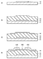
図1は、本発明の第1の実施の形態に係る薄膜トランジスタ1の断面構造を表すものである。薄膜トランジスタ1は、例えばボトムゲート型の構造を有し、チャネル領域(活性層)に酸化物半導体を用いたものである。薄膜トランジスタ1は、ガラスやプラスティックなどよりなる基板11上にゲート電極12を有しており、このゲート電極12と基板11とを覆うように、ゲート絶縁膜13が設けられている。ゲート絶縁膜13上のゲート電極12に対応する領域には、酸化物半導体膜14が形成され、酸化物半導体膜14上には、所定の間隔をおいて一対の電極(ソース電極15Aおよびドレイン電極15B)が設けられている。これらの酸化物半導体膜14のチャネル領域14A、ソース電極15Aおよびドレイン電極15Bを被覆するように、基板11の全面に渡って保護膜16が形成されている。
[First Embodiment]
FIG. 1 shows a cross-sectional structure of a thin film transistor 1 according to the first embodiment of the present invention. The thin film transistor 1 has a bottom gate structure, for example, and uses an oxide semiconductor for a channel region (active layer). The thin film transistor 1 has a
ゲート電極12は、薄膜トランジスタ1に印加されるゲート電圧により酸化物半導体膜14中の電子密度を制御する役割を果たすものである。このゲート電極12は、例えばモリブデン(Mo)などから構成されている。
The
ゲート絶縁膜13は、シリコン酸化膜、シリコン窒化膜、シリコン窒化酸化膜、あるいは酸化アルミニウム膜等により構成されている。
The
酸化物半導体膜14は、酸化物半導体から構成され、電圧印加によりソース電極15Aとドレイン電極15Bとの間にチャネル領域14Aを形成するようになっている。ここで、酸化物半導体とは、インジウム(In)、ガリウム(Ga)、亜鉛(Zn)、スズ(Su)等の元素から形成された酸化物である。この酸化物半導体膜14は、厚みが例えば20nm〜100nmである。
The
ソース電極15Aおよびドレイン電極15Bは、例えばモリブデンやクロム(Cr)単体、もしくはチタン(Ti)/アルミニウム(Al)/チタンの積層構造により構成されている。
The
保護膜16は、薄膜トランジスタ1の内部、特に酸化物半導体膜14のチャネル領域14Aへの水素などの浸入を抑制するものである。この保護膜16は、酸化アルミニウム膜(Al2O3)を含むものであり、単層膜または2層以上の積層膜により構成される。2層膜としては、例えば、酸化アルミニウム膜とシリコン窒化膜との積層膜、あるいは酸化アルミニウム膜とシリコン酸化膜との積層膜が挙げられる。3層膜としては、例えば、酸化アルミニウム膜とシリコン窒化膜とシリコン酸化膜との積層膜が挙げられる。この保護膜16の厚みは、例えば10nm〜100nmであり、好ましくは50nm以下である。
The protective film 16 suppresses intrusion of hydrogen or the like into the thin film transistor 1, particularly into the
上記薄膜トランジスタ1は、例えば次のようにして製造することができる。 The thin film transistor 1 can be manufactured as follows, for example.
まず、図2(A)に示したように、基板11上の全面にスパッタリング法や蒸着法により金属薄膜を形成したのち、この金属薄膜を、例えばフォトリレジストを用いたエッチングによりパターニングすることにより、ゲート電極12を形成する。
First, as shown in FIG. 2A, after forming a metal thin film on the entire surface of the
続いて、図2(B)に示したように、基板11およびゲート電極12上を覆うようにゲート絶縁膜13を、例えばプラズマCVD(Chemical Vapor Deposition;化学気相成長)法により形成する。
Subsequently, as shown in FIG. 2B, a
続いて、図2(C)に示したように、上述した材料および厚みからなる酸化物半導体膜14を、例えばスパッタリング法により形成する。例えば、酸化物半導体として酸化インジウムガリウム亜鉛(IGZO)を用いた場合には、酸化インジウムガリウム亜鉛のセラミックをターゲットとしたDCスパッタ法を用い、アルゴン(Ar)および酸素(O2)の混合ガスを用いたプラズマ放電により、酸化物半導体膜14を形成する。但し、プラズマ放電を行う前に、真空容器内の真空度が、例えば1×10⁻⁴Pa以下になるまで排気したのち、アルゴンと酸素の混合ガスを導入するようにするとよい。こののち、形成した酸化物半導体膜14を、例えばフォレジストを用いたエッチングによりパターニングする。
Subsequently, as illustrated in FIG. 2C, the
続いて、図2(D)に示したように、酸化物半導体膜14上に金属薄膜を例えばスパッタリング法により形成したのち、この金属薄膜のうち酸化物半導体膜14のチャネル領域14Aに対応する領域に、例えばフォトレジストを用いたエッチングにより、開口150を形成する。これにより、ソース電極15Aおよびドレイン電極15Bがそれぞれ形成される。
Subsequently, as shown in FIG. 2D, after a metal thin film is formed on the
次いで、形成した酸化物半導体膜14、ソース電極15Aおよびドレイン電極15Bを被覆するように、上述した材料等よりなる保護膜16を形成する。なお、ここでは、保護膜16として、酸化アルミニウム膜単層を形成する場合について説明する。この保護膜16は、例えば以下に説明するような原子層成膜(ALD:Atomic Layer Deposition)法を用いて形成する。すなわち、酸化物半導体膜14、ソース電極15Aおよびドレイン電極15Bを形成した基板11を、真空チャンバー内に配置し、原料ガスとなるトリメチルアルミニウムガスを導入して、電極形成側に原子層のアルミニウム膜を形成する。続いて、オゾンガスあるいは酸素ガスをプラズマで励起した酸素ラジカルを、基板11のアルミニウム膜が形成された側へ導入することにより、アルミニウム膜を酸化する。ここで、上記アルミニウム膜は、原子層レベルの膜厚であるため、オゾンあるいは酸素ラジカルによって容易に酸化される。これにより、基板11の全面に渡って酸化アルミニウム膜が形成される。このようにして、アルミニウム膜の原子層形成プロセスと酸化プロセスとを交互に繰り返すことで、所望の膜厚の酸化アルミニウム膜を形成することが可能である。
Next, the protective film 16 made of the above-described material or the like is formed so as to cover the formed
このように、保護膜16としての酸化アルミニウム膜を、原子層成膜法を用いて形成することにより、酸化プロセスにおいて酸素不足となることがないため、化学量論比となる理想的な組成を実現し易くなる。例えば、アルミニウムと酸素の組成比を、理想的な2:3とすることが可能である。また、水素ガスの発生を抑制した状態で成膜可能であるため、酸化物半導体膜14の電気的特性を劣化させることがない。これにより、優れたガスバリア性を有する保護膜16を形成することができる。以上により、図1に示した薄膜トランジスタ1を完成する。
In this way, by forming the aluminum oxide film as the protective film 16 by using the atomic layer deposition method, oxygen is not deficient in the oxidation process. Therefore, an ideal composition that provides a stoichiometric ratio is obtained. It becomes easy to realize. For example, the composition ratio of aluminum and oxygen can be an ideal 2: 3. In addition, since the film can be formed in a state where generation of hydrogen gas is suppressed, the electrical characteristics of the
次いで、本実施の形態の薄膜トランジスタ1の作用、効果について説明する。 Next, functions and effects of the thin film transistor 1 of the present embodiment will be described.
薄膜トランジスタ1では、図示しない配線層を通じてゲート電極12とソース電極15Aとの間に所定のしきい値電圧以上のゲート電圧Vgが印加されると、酸化物半導体膜14にチャネル領域14Aが形成され、ソース電極15Aとドレイン電極15Bとの間に電流(ドレイン電流Id)が流れ、トランジスタとして機能する。
In the thin film transistor 1, when a gate voltage Vg equal to or higher than a predetermined threshold voltage is applied between the
ここで、薄膜トランジスタ1の内部へ水素などの元素が浸入した場合、前述のように、酸化物半導体膜14において、電気的に浅い不純物準位が形成され、低抵抗化を生じる。このため、例えば酸化物半導体膜14として酸化亜鉛を用いた場合、ゲート電圧Vgを印加しなくてもドレイン電流Idが流れ、リーク電流が増大してしまう。
Here, when an element such as hydrogen enters the thin film transistor 1, as described above, an electrically shallow impurity level is formed in the
これに対し、本実施の形態では、酸化アルミニウム膜からなる保護膜16を、チャネル領域14A、ソース電極15Aおよびドレイン電極15Bを被覆するように設けることにより、酸化アルミニウム膜のガスバリア性によって、酸化物半導体膜14への水素の浸入が抑制される。これにより、上記のようなリーク電流の発生を抑制することができる。また、この酸化アルミニウム膜を、上述したような原子層成膜法により形成することにより、より優れたガスバリア性を実現することができる。よって、リーク電流の発生を効果的に抑制することができる。
On the other hand, in the present embodiment, the protective film 16 made of an aluminum oxide film is provided so as to cover the
以上説明したような薄膜トランジスタ1は、例えば有機ELディスプレイや液晶ディスプレイなどの表示装置における駆動素子として好適に用いることができる。このような表示装置では、上記薄膜トランジスタ1を備えていることにより、リーク電流を抑制することができるため、輝度の高い明るい表示を実現できる。更に酸化アルミニウム膜による保護膜16が外部からの水素などの浸入を防ぐため、信頼性が向上する。 The thin film transistor 1 as described above can be suitably used as a driving element in a display device such as an organic EL display or a liquid crystal display. In such a display device, since the thin film transistor 1 is provided, leakage current can be suppressed, so that a bright display with high luminance can be realized. Furthermore, since the protective film 16 made of an aluminum oxide film prevents intrusion of hydrogen or the like from the outside, the reliability is improved.
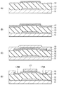
[第2の実施の形態]
図3は、本発明の第2の実施の形態に係る薄膜トランジスタ2の断面構造を表すものである。薄膜トランジスタ2は、上記第1の実施の形態と同様、ボトムゲート型の構造を有し、チャネル領域(活性層)に酸化物半導体を用いたものである。以下では、上記第1の実施の形態と同様の構成要素については同一の符号を付し、適宜説明を省略する。
[Second Embodiment]
FIG. 3 shows a cross-sectional structure of the
薄膜トランジスタ2では、基板11上にゲート電極12、ゲート絶縁膜13および酸化物半導体膜14が設けられている。本実施の形態では、酸化物半導体膜14の上面には、チャネル保護膜17(第1の保護膜)が形成され、このチャネル保護膜17の上面と酸化物半導体膜14の側面とを被覆するように、保護膜18(第2の保護膜)が形成されている。チャネル保護膜17および保護膜18には、開口170A,170Bが設けられ、これら開口170A,170Bに、ソース電極19Aおよびドレイン電極19Bがそれぞれ埋設されている。
In the
チャネル保護膜17は、酸化物半導体14の上面を覆うように形成されている。このチャネル保護膜17は、酸化物半導体膜14の機械的損傷を防止すると共に、例えば製造プロセス中の熱処理などにより、酸化物半導体膜14中の酸素などの脱離を抑制する役割を果たしている。また、製造プロセスにおいて、酸化物半導体膜14をレジスト剥離液から保護するという役割も果たしている。このようなチャネル保護膜17は、上記第1の実施の形態の保護膜16と同様の材料により構成されている。
The channel
保護膜18は、薄膜トランジスタ2内部を保護する目的で設けられ、上記第1の実施の形態の保護膜16と同様の材料により構成されている。
The
上記薄膜トランジスタ2は、例えば次のようにして製造することができる。
The
まず、図4(A)に示したように、ゲート絶縁膜13の全面に、上述した手法により酸化物半導体膜14を形成する。
First, as illustrated in FIG. 4A, the
続いて、図4(B)に示したように、形成した酸化物半導体膜14の全面にチャネル保護膜17を、例えば上述したような原子層成膜法により形成する。
Subsequently, as shown in FIG. 4B, the channel
続いて、図4(C)に示したように、全面に渡って形成したチャネル保護膜17および酸化物半導体膜14を、フォトレジストを用いたエッチングによりパターニングする。こののち、パターニングしたチャネル保護膜の上面および酸化物半導体膜14の側面を被覆するように、保護膜18を上述した原子層成膜法により形成する。
Subsequently, as shown in FIG. 4C, the channel
続いて、図4(D)に示したように、形成したチャネル保護膜17および保護膜18に、例えばフォトレジストを用いたエッチングにより、酸化物半導体膜14の表面まで貫通する開口170A,170Bを形成する。
Subsequently, as shown in FIG. 4D,
最後に、これらの開口170A,170Bを埋めるように、金属薄膜を例えばスパッタリング法により形成する。こののち、形成した金属薄膜のチャネル領域14Aに対応する領域に、例えばフォトレジストを用いたエッチングにより、開口を形成する。これにより、ソース電極19Aおよびドレイン電極19Bがそれぞれ形成される。以上により、図3に示した薄膜トランジスタ2を完成する。
Finally, a metal thin film is formed by, for example, a sputtering method so as to fill the
上記第2の実施の形態の薄膜トランジスタ2では、酸化物半導体膜14の上面を覆うように形成したチャネル保護膜17により、酸化物半導体14、ソース電極19Aおよびドレイン電極19Bをパターニング形成する際のエッチングによってチャネル領域14Aが損傷することを防止することができる。また、チャネル保護膜17の上面と酸化物半導体膜14の側面とを被覆するように設けられた保護膜18により、酸化物半導体膜14への水素の浸入を抑制することができる。よって、上記第1の実施の形態よりも、効果的にリーク電流の発生を抑制することができる。
In the
[第3の実施の形態]
図5は、本発明の第3の実施の形態に係る薄膜トランジスタ3の断面構造を表すものである。薄膜トランジスタ3は、上記第1の実施の形態と同様、ボトムゲート型の構造を有し、チャネル領域(活性層)に酸化物半導体を用いたものである。以下では、上記第1の実施の形態と同様の構成要素については同一の符号を付し、適宜説明を省略する。
[Third Embodiment]
FIG. 5 shows a cross-sectional structure of the
薄膜トランジスタ3では、基板11上にゲート電極12、ゲート絶縁膜13および酸化物半導体膜14が設けられている。酸化物半導体膜14上のチャネル領域14Aに対応する領域には、チャネル保護膜20(第1の保護膜)が形成されている。本実施の形態では、ソース電極21Aおよびドレイン電極21Bが、チャネル保護膜20の端部を覆うようにして酸化物半導体膜14上に設けられている。また、これらのチャネル保護膜20、ソース電極21Aおよびドレイン電極21Bを被覆するように保護膜22(第2の保護膜)が形成されている。
In the
チャネル保護膜20は、酸化物半導体膜14の機械的損傷を防止すると共に、例えば製造プロセス中の熱処理などにおいて酸素などの元素が脱離することを抑制する役割を果たしている。また、製造プロセスにおいて、酸化物半導体膜14をレジスト剥離液から保護するという役割も果たしている。本実施の形態では、このチャネル保護膜20がシリコン酸化膜により構成されている。
The channel
保護膜22は、薄膜トランジスタ3内部を保護する目的で設けられ、上記第1の実施の形態の保護膜16と同様の材料により構成されている。
The protective film 22 is provided for the purpose of protecting the inside of the
上記薄膜トランジスタ3は、例えば次のようにして製造することができる。
The
まず、図6(A)に示したように、ゲート絶縁膜13の全面に、上述した手法により酸化物半導体膜14を形成したのち、上述した材料よりなるチャネル保護膜20を、例えばプラズマCVD法により形成する。なお、本実施の形態では、この後の工程において、酸素雰囲気でアニール処理することが望ましい。一般に、酸化物半導体膜は、真空雰囲気中に置かれることにより、膜中や表面に存在する酸素が脱離してしまうことが知られている。シリコン酸化膜は、酸素拡散性を有するため、チャネル保護膜20をシリコン酸化膜により形成し、酸化物半導体膜14に対して酸素雰囲気でアニール処理を施すことにより、酸化物半導体膜14に酸素を供給することが可能となる。これにより、酸化物半導体膜14における格子欠陥の発生を抑制することができる。
First, as shown in FIG. 6A, after the
続いて、図6(B)に示したように、全面に渡って形成したチャネル保護膜20および酸化物半導体膜14を、順に、フォトレジストを用いたエッチングによりパターニングする。
Subsequently, as shown in FIG. 6B, the channel
続いて、図6(C)に示したように、形成したチャネル保護膜20および酸化物半導体膜14を覆うように、金属薄膜を例えばスパッタリング法により成膜する。こののち、金属薄膜のチャネル領域14Aに対応する領域に、例えばフォトレジストを用いたエッチングにより、開口を形成する。これにより、ソース電極21Aおよびドレイン電極21Bがそれぞれ形成される。
Subsequently, as illustrated in FIG. 6C, a metal thin film is formed by, for example, a sputtering method so as to cover the formed channel
一方、保護膜22を形成する前段階の処理として、酸化物半導体膜14に対し、例えばオゾン処理、酸素プラズマ処理もしくは二酸化窒素プラズマ処理を施す。このような処理は、酸化物半導体膜14を形成した後、保護膜22を形成する前であれば、どのタイミングで行うようにしてもよい。但し、保護膜22を形成する直前に行うことが望ましい。このような前処理を行うことによっても、酸化物半導体膜14における格子欠陥の発生を抑制することができる。
On the other hand, for example, ozone treatment, oxygen plasma treatment, or nitrogen dioxide plasma treatment is performed on the
最後に、形成したチャネル保護膜20、ソース電極21Aおよびドレイン電極21Bを覆うように、保護膜22を例えば上述した原子層成膜法により形成する。以上により、図5に示した薄膜トランジスタ3を完成する。
Finally, the protective film 22 is formed by, for example, the atomic layer deposition method described above so as to cover the formed channel
上記第3の実施の形態の薄膜トランジスタ3では、酸化物半導体膜14のチャネル領域14A上に形成したチャネル保護膜20により、例えばソース電極19Aおよびドレイン電極19Bを形成する際のエッチングにより、チャネル領域14Aが損傷することを防止することができる。また、チャネル保護膜20、ソース電極21Aおよびドレイン電極21Bを覆うように設けられた保護膜22により、酸化物半導体膜14への水素の浸入を抑制することができる。よって、上記第1の実施の形態よりも、リーク電流の発生を効果的に抑制することができる。
In the
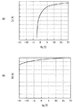
また、チャネル保護膜20をシリコン酸化膜により形成し、酸素雰囲気でアニール処理を施すことにより、もしくは、保護膜22形成前にオゾン処理等を施すことにより、酸化物半導体膜14における格子欠陥の発生を抑制することができる。ここで、保護膜22の形成前にオゾン処理を行った場合の薄膜トランジスタ3の電流(Id)−電圧(Vg)特性を、図7(A)に示す。また、オゾン処理を行なわなかった場合の電流−電圧特性を図7(B)に示す。
In addition, by forming the channel
図7(A)に示したように、オゾン処理を行うことにより、低いオフリーク電流を得ることが可能となり、十分に高いオンオフ比を有する電気特性を得ることが可能となる。一方、図7(B)に示したように、オゾン処理を行わない場合には、トランジスタのしきい値電圧がマイナス方向にシフトしてしまい電気特性が大きく劣化してしまうことがわかる。これは、次のような理由によるものと考えられる。一般に、酸化物半導体膜では、真空中において膜中や表面の酸素が脱離し、これにより格子欠陥が発生する。このような格子欠陥は、水素ガスと同様、酸化物半導体膜中に浅い不純物準位を形成し、リーク電流を増大させてしまう。また、キャリアの誘起を妨げて、キャリア濃度を減少させる。このキャリア濃度の減少は、酸化物半導体膜の導電率を引き下げ、薄膜トランジスタの電子移動度、電流伝達特性(例えば、サブスレッショルド特性やしきい電圧)に影響する。よって、保護膜22の形成前にオゾン処理を施すことで、酸化物半導体膜14中に十分な量の酸素を供給することが可能となり、格子欠陥の発生を抑制し、結果的にオフリーク電流が低く十分なオンオフ比を有する薄膜トランジスタ3を得ることができる。なお、オゾン処理の代わりに酸素ガスや二酸化窒素ガスをプラズマで励起して形成したラジカルで処理を行った場合においても上記と同等の効果を得ることができる。
As shown in FIG. 7A, by performing the ozone treatment, a low off-leakage current can be obtained, and electrical characteristics having a sufficiently high on-off ratio can be obtained. On the other hand, as shown in FIG. 7B, it can be seen that when the ozone treatment is not performed, the threshold voltage of the transistor shifts in the negative direction and the electrical characteristics are greatly deteriorated. This is considered due to the following reasons. In general, in an oxide semiconductor film, oxygen in the film or on the surface is desorbed in a vacuum, thereby generating lattice defects. Such a lattice defect, like hydrogen gas, forms a shallow impurity level in the oxide semiconductor film and increases leakage current. In addition, the carrier concentration is reduced by preventing the induction of carriers. This decrease in carrier concentration lowers the conductivity of the oxide semiconductor film and affects the electron mobility and current transfer characteristics (eg, subthreshold characteristics and threshold voltage) of the thin film transistor. Therefore, by performing ozone treatment before the formation of the protective film 22, it is possible to supply a sufficient amount of oxygen into the
また、図8に、保護膜22としての酸化アルミニウム膜の膜厚に対する薄膜トランジスタ3のオフリーク電流の関係を示す。但し、保護膜22の形成前に上記オゾン処理を施したものである。このように、保護膜22の膜厚が50nmより大きくなると、オゾン処理を行ってもオフリーク電流が増加してしまい、十分なオンオフ比が得られないことがわかる。このことから、保護膜22として用いる酸化アルミニウム膜の膜厚は50nm以下とすることが望ましい。
FIG. 8 shows the relationship between the off-leakage current of the
さらに、図9(A),(B)に、膜厚10nmの酸化アルミニウム膜の保護膜22を形成した場合の薄膜トランジスタ3の電流−電圧特性を示す。但し、図9(A)は、初期の特性、図9(B)は、窒素雰囲気中、温度300℃で1時間アニールした後の特性である。また、これらの比較例として、保護膜22を形成しない場合の初期の特性を図10(A)、窒素雰囲気中、温度300℃で1時間アニールした後の特性を図10(B)に示す。
Further, FIGS. 9A and 9B show current-voltage characteristics of the
図10(A),(B)に示したように、保護膜22を形成しない場合には、アニール後に電流−電圧特性が大きく変化して、オフリーク電流が急激に増大していることがわかる。これに対して、図9(A),(B)に示したように、膜厚10nmの酸化アルミニウム膜を保護膜22として形成した本実施の形態の薄膜トランジスタ3では、300℃のアニールの後においても特性に変化はほとんど見られず、安定していることがわかる。これにより、デバイス作製の際に必要となる熱プロセスに対してもトランジスタ特性を劣化させることなく、安定した特性を維持できることがわかった。
As shown in FIGS. 10A and 10B, it can be seen that when the protective film 22 is not formed, the current-voltage characteristics change greatly after annealing, and the off-leakage current increases rapidly. On the other hand, as shown in FIGS. 9A and 9B, in the
(変形例)
次に、上記第3の実施の形態の変形例について説明する。図11は、変形例に係る薄膜トランジスタ4の断面構造を表すものである。薄膜トランジスタ4は、上記第1の実施の形態と同様、ボトムゲート型の構造を有し、チャネル領域(活性層)に酸化物半導体を用いたものである。以下では、上記第1および第3の実施の形態と同様の構成要素については同一の符号を付し、適宜説明を省略する。
(Modification)
Next, a modification of the third embodiment will be described. FIG. 11 shows a cross-sectional structure of a
本変形例では、ソース電極23Aおよびドレイン電極23Bの構成以外は、上記第3の実施の形態と同様の構成となっている。すなわち、ソース電極23Aおよびドレイン電極23Bは、酸化物半導体膜14上に形成されたチャネル保護膜20と互いに重ならないように設けられている。保護膜24は、酸化物半導体膜14の一部と、チャネル保護膜20と、ソース電極23Aおよびドレイン電極23Bとを覆うように形成されている。保護膜24は、薄膜トランジスタ4内部を保護する目的で設けられ、上記第1の実施の形態の保護膜16と同様の材料等により構成されている。
In the present modification, the configuration is the same as that of the third embodiment except for the configuration of the
この薄膜トランジスタ4は、例えば次のようにして製造することができる。まず、図12(A)に示したように、上述した第3の実施の形態の薄膜トランジスタ3と同様にして、チャネル保護膜20および酸化物半導体膜14を順に、フォトレジストを用いたエッチングによりパターニング形成する。続いて、図12(B)に示したように、形成したチャネル保護膜20と重ならないように、酸化物半導体膜14上に、ソース電極23Aおよびドレイン電極23Bを形成する。最後に、保護膜24を上述した原子層成膜法により形成する。なお、本変形例においても、上記第3の実施の形態と同様に、保護膜24形成前にオゾン処理等を施すことが望ましい。以上により、図11に示した薄膜トランジスタ4を完成する。
The
上記のように、ソース電極23Aおよびドレイン電極23Bは、チャネル保護膜20と重ならないように形成されていてもよい。このように構成した場合であっても、上記第1および第3の実施の形態と同等の効果を得ることができる。なお、酸化物半導体膜14に、チャネル保護膜20とソース電極23Aおよびドレイン電極23Bの両方に被覆されない領域(露出領域)が存在することになるが、保護膜24を形成する際の減圧雰囲気中において、この露出領域における酸素は脱離してしまうため、露出領域では低抵抗となる。よって、寄生抵抗により薄膜トランジスタ5の電流を低下させることなく寄生容量を低減させることができる。
As described above, the source electrode 23 </ b> A and the drain electrode 23 </ b> B may be formed so as not to overlap with the channel
なお、ここでの保護膜形成前のオゾン処理等は、上記第1および第2の実施の形態の薄膜トランジスタの製造プロセスにおいても行うことができる。また、上記第2の実施の形態では、チャネル保護膜17を酸化アルミニウム膜により形成する場合を例に挙げて説明したが、これに限定されず、上記第3の実施の形態および変形例のように、チャネル保護膜17をシリコン酸化膜により形成し、後の工程において酸素雰囲気中でアニール処理を施すようにしてもよい。また、上記第3の実施の形態および変形例では、チャネル保護膜20がシリコン酸化膜により構成された場合を例に挙げて説明したが、酸化アルミニウム膜により構成されていてもよい。
Here, the ozone treatment before the formation of the protective film can be performed also in the manufacturing process of the thin film transistor of the first and second embodiments. In the second embodiment, the case where the channel
以上、実施の形態および変形例を挙げて本発明を説明したが、本発明は上記実施の形態等に限定されず、種々の変形が可能である。例えば、上記実施の形態等では、酸化アルミニウム膜を、原子層成膜法により形成する場合を例に挙げて説明したが、これに限定されず、他の成膜方法、例えばスパッタリング法などにより酸化アルミニウム膜を形成するようにしてもよい。但し、上述したように、原子層成膜法を用いた場合、酸化アルミニウム膜を理想的な組成比で均一に形成することができるため、ガスバリア性を確保し易くなる。 Although the present invention has been described with reference to the embodiment and the modifications, the present invention is not limited to the above-described embodiment and the like, and various modifications can be made. For example, in the above embodiment and the like, the case where the aluminum oxide film is formed by the atomic layer deposition method has been described as an example. However, the present invention is not limited to this, and the oxidation is performed by another deposition method such as a sputtering method. An aluminum film may be formed. However, as described above, when the atomic layer deposition method is used, an aluminum oxide film can be uniformly formed with an ideal composition ratio, and thus it is easy to ensure gas barrier properties.
また、上記実施の形態等では、薄膜トランジスタとして、ボトムゲート構造を例に挙げて説明したが、これに限定されず、トップゲート構造であってもよい。 In the above-described embodiments and the like, the bottom gate structure is described as an example of the thin film transistor. However, the present invention is not limited to this, and a top gate structure may be used.
1〜4…薄膜トランジスタ、11…基板、12…ゲート電極、13…ゲート絶縁膜、14…酸化物半導体膜、15A,19A,21A,23A…ソース電極、15B,19B,21B,23b…ドレイン電極、16,18,22,24…保護膜、17,20…チャネル保護膜。 DESCRIPTION OF SYMBOLS 1-4 ... Thin-film transistor, 11 ... Substrate, 12 ... Gate electrode, 13 ... Gate insulating film, 14 ... Oxide semiconductor film, 15A, 19A, 21A, 23A ... Source electrode, 15B, 19B, 21B, 23b ... Drain electrode, 16, 18, 22, 24 ... protective film, 17, 20 ... channel protective film.
Claims (15)
前記ゲート電極に対応してチャネル領域を形成する酸化物半導体膜と、
前記酸化物半導体膜上に形成されたソース電極およびドレイン電極からなる一対の電極と、
前記酸化物半導体膜のチャネル領域に対向して設けられた一または複数の保護膜とを備え、
前記一または複数の保護膜のうち少なくとも一の保護膜が酸化アルミニウムを含んで構成されている
薄膜トランジスタ。 A gate electrode;
An oxide semiconductor film that forms a channel region corresponding to the gate electrode;
A pair of electrodes consisting of a source electrode and a drain electrode formed on the oxide semiconductor film;
One or more protective films provided to face the channel region of the oxide semiconductor film,
A thin film transistor in which at least one of the one or more protective films includes aluminum oxide.
請求項1に記載の薄膜トランジスタ。 The thin film transistor according to claim 1, wherein the protective film is made of an aluminum oxide film.
請求項1に記載の薄膜トランジスタ。 The thin film transistor according to claim 1, wherein the protective film is formed of a laminated film of an aluminum oxide film and at least one of a silicon nitride film and a silicon oxide film.
請求項2または3に記載の薄膜トランジスタ。 The thin film transistor according to claim 2 or 3, wherein the aluminum oxide film has a thickness of 50 nm or less.
請求項1に記載の薄膜トランジスタ。 The thin film transistor according to claim 1, wherein the protective film is formed to cover a channel region of the oxide semiconductor film and the pair of electrodes.
前記酸化物半導体膜の上面を覆うように形成された第1の保護膜と、
前記第1の保護膜の上面および前記酸化物半導体膜の側面を覆うように形成された第2の保護膜とを有し、
前記第1および第2の保護膜は開口を有し、
前記一対の電極は、前記開口を介して前記酸化物半導体膜上に形成され、かつ
前記第1および第2の保護膜のうち少なくともいずれか一方が、酸化アルミニウムを含む
請求項1に記載の薄膜トランジスタ。 The protective film is
A first protective film formed to cover the upper surface of the oxide semiconductor film;
A second protective film formed so as to cover an upper surface of the first protective film and a side surface of the oxide semiconductor film;
The first and second protective films have openings;
2. The thin film transistor according to claim 1, wherein the pair of electrodes is formed on the oxide semiconductor film through the opening, and at least one of the first and second protective films includes aluminum oxide. .
前記酸化物半導体膜のチャネル領域上に形成された第1の保護膜と、
前記第1の保護膜および前記一対の電極を覆うように形成された第2の保護膜とを有し、
前記第1および第2の保護膜のうち少なくともいずれか一方が、酸化アルミニウムを含む
請求項1に記載の薄膜トランジスタ。 The protective film is
A first protective film formed on a channel region of the oxide semiconductor film;
A second protective film formed to cover the first protective film and the pair of electrodes;
The thin film transistor according to claim 1, wherein at least one of the first and second protective films contains aluminum oxide.
請求項7に記載の薄膜トランジスタ。 The thin film transistor according to claim 7, wherein the second protective film includes aluminum oxide.
請求項7に記載の薄膜トランジスタ。 The thin film transistor according to claim 7, wherein the pair of electrodes are formed on the oxide semiconductor film so as to cover an end portion of the first protective film.
請求項7に記載の薄膜トランジスタ。 The thin film transistor according to claim 7, wherein the pair of electrodes are formed so as not to overlap the first protective film over the oxide semiconductor film.
前記ゲート電極に対応してチャネル領域を有する酸化物半導体膜を形成する工程と、
前記酸化物半導体膜上にソース電極およびドレイン電極からなる一対の電極を形成する工程と、
前記酸化物半導体膜のチャネル領域に対向するように、一または複数の保護膜を形成する工程とを含み、
前記一または複数の保護膜のうち少なくとも一の保護膜を、酸化アルミニウムを含む膜により形成する
薄膜トランジスタの製造方法。 Forming a gate electrode on the substrate;
Forming an oxide semiconductor film having a channel region corresponding to the gate electrode;
Forming a pair of electrodes consisting of a source electrode and a drain electrode on the oxide semiconductor film;
Forming one or more protective films so as to face the channel region of the oxide semiconductor film,
A method for manufacturing a thin film transistor, wherein at least one of the one or more protective films is formed of a film containing aluminum oxide.
請求項11に記載の薄膜トランジスタの製造方法。 The method for manufacturing a thin film transistor according to claim 11, wherein the film containing aluminum oxide is formed by an atomic layer deposition method.
請求項11に記載の薄膜トランジスタの製造方法。 The method for manufacturing a thin film transistor according to claim 11, wherein an ozone treatment, an oxygen plasma treatment, or a nitrogen dioxide plasma treatment is performed on the oxide semiconductor film before forming the film containing aluminum oxide.
前記酸化物半導体膜のチャネル領域上に、シリコン酸化膜を含む第1の保護膜を形成する工程と、
前記第1の保護膜を形成した後、前記酸化物半導体膜に対して酸素雰囲気中でアニール処理を施す工程と、
前記第1の保護膜および前記一対の電極を覆うように、酸化アルミニウムを含む第2の保護膜を形成する工程と
を含む請求項11に記載の薄膜トランジスタの製造方法。 The step of forming the one or more protective films includes:
Forming a first protective film including a silicon oxide film on the channel region of the oxide semiconductor film;
After forming the first protective film, annealing the oxide semiconductor film in an oxygen atmosphere; and
Forming a second protective film containing aluminum oxide so as to cover the first protective film and the pair of electrodes.
前記薄膜トランジスタは、
ゲート電極と、
前記ゲート電極に対応してチャネル領域を形成する酸化物半導体膜と、
前記酸化物半導体膜上に形成されたソース電極およびドレイン電極からなる一対の電極と、
前記酸化物半導体膜のチャネル領域に対向して設けられた一または複数の保護膜とを有し、
前記一または複数の保護膜のうち少なくとも一の保護膜が酸化アルミニウムを含んで構成されている
表示装置。
A display element, and a thin film transistor for driving the display element,
The thin film transistor
A gate electrode;
An oxide semiconductor film forming a channel region corresponding to the gate electrode;
A pair of electrodes consisting of a source electrode and a drain electrode formed on the oxide semiconductor film;
One or a plurality of protective films provided opposite to the channel region of the oxide semiconductor film,
A display device in which at least one of the one or more protective films includes aluminum oxide.
Priority Applications (5)
| Application Number | Priority Date | Filing Date | Title |
|---|---|---|---|
| JP2008174469A JP5584960B2 (en) | 2008-07-03 | 2008-07-03 | Thin film transistor and display device |
| PCT/JP2009/061507 WO2010001783A1 (en) | 2008-07-03 | 2009-06-24 | Thin film transistor and display device |
| KR1020107029079A KR20110025768A (en) | 2008-07-03 | 2009-06-24 | Thin film transistor and display device |
| CN2009801256879A CN102084486A (en) | 2008-07-03 | 2009-06-24 | Thin film transistor and display device |
| US13/000,446 US20110095288A1 (en) | 2008-07-03 | 2009-06-24 | Thin film transistor and display device |
Applications Claiming Priority (1)
| Application Number | Priority Date | Filing Date | Title |
|---|---|---|---|
| JP2008174469A JP5584960B2 (en) | 2008-07-03 | 2008-07-03 | Thin film transistor and display device |
Publications (3)
| Publication Number | Publication Date |
|---|---|
| JP2010016163A true JP2010016163A (en) | 2010-01-21 |
| JP2010016163A5 JP2010016163A5 (en) | 2011-08-04 |
| JP5584960B2 JP5584960B2 (en) | 2014-09-10 |
Family
ID=41465881
Family Applications (1)
| Application Number | Title | Priority Date | Filing Date |
|---|---|---|---|
| JP2008174469A Active JP5584960B2 (en) | 2008-07-03 | 2008-07-03 | Thin film transistor and display device |
Country Status (5)
| Country | Link |
|---|---|
| US (1) | US20110095288A1 (en) |
| JP (1) | JP5584960B2 (en) |
| KR (1) | KR20110025768A (en) |
| CN (1) | CN102084486A (en) |
| WO (1) | WO2010001783A1 (en) |
Cited By (66)
| Publication number | Priority date | Publication date | Assignee | Title |
|---|---|---|---|---|
| JP2010135762A (en) * | 2008-10-31 | 2010-06-17 | Semiconductor Energy Lab Co Ltd | Driver circuit and display device |
| WO2011099359A1 (en) * | 2010-02-12 | 2011-08-18 | Semiconductor Energy Laboratory Co., Ltd. | Display device and driving method |
| WO2011111502A1 (en) * | 2010-03-08 | 2011-09-15 | Semiconductor Energy Laboratory Co., Ltd. | Display device |
| JP2011187952A (en) * | 2010-02-12 | 2011-09-22 | Semiconductor Energy Lab Co Ltd | Semiconductor device and method of manufacturing the same |
| JP2011216574A (en) * | 2010-03-31 | 2011-10-27 | Japan Science & Technology Agency | Thin film transistor and method for manufacturing the same |
| WO2011135987A1 (en) * | 2010-04-28 | 2011-11-03 | Semiconductor Energy Laboratory Co., Ltd. | Method for manufacturing semiconductor device |
| JP2011233882A (en) * | 2010-04-07 | 2011-11-17 | Semiconductor Energy Lab Co Ltd | Transistor |
| JP2011243973A (en) * | 2010-04-23 | 2011-12-01 | Semiconductor Energy Lab Co Ltd | Method for manufacturing semiconductor device |
| WO2011155125A1 (en) * | 2010-06-08 | 2011-12-15 | シャープ株式会社 | Thin film transistor substrate, liquid crystal display device provided with same, and thin film transistor substrate production method |
| JP2011258939A (en) * | 2010-05-14 | 2011-12-22 | Semiconductor Energy Lab Co Ltd | Method for manufacturing semiconductor device |
| JP2012019207A (en) * | 2010-06-11 | 2012-01-26 | Semiconductor Energy Lab Co Ltd | Semiconductor device and manufacturing method of semiconductor device |
| JP2012053971A (en) * | 2010-08-06 | 2012-03-15 | Semiconductor Energy Lab Co Ltd | Semiconductor device |
| JP2012109516A (en) * | 2010-11-15 | 2012-06-07 | Samsung Mobile Display Co Ltd | Oxide semiconductor thin film transistor and manufacturing method for the same |
| JP2012160716A (en) * | 2011-01-12 | 2012-08-23 | Semiconductor Energy Lab Co Ltd | Manufacturing method for semiconductor device |
| JP2012178545A (en) * | 2010-12-01 | 2012-09-13 | Semiconductor Energy Lab Co Ltd | Semiconductor device and manufacturing method for semiconductor device |
| JP2012182388A (en) * | 2011-03-02 | 2012-09-20 | Toshiba Corp | Thin-film transistor, method of manufacturing the same, and display device |
| JP2012209546A (en) * | 2011-03-11 | 2012-10-25 | Semiconductor Energy Lab Co Ltd | Manufacturing method for semiconductor device |
| KR20120129795A (en) * | 2011-05-19 | 2012-11-28 | 가부시키가이샤 한도오따이 에네루기 켄큐쇼 | Method for manufacturing semiconductor device |
| CN102822980A (en) * | 2010-03-26 | 2012-12-12 | 株式会社半导体能源研究所 | Method for manufacturing semiconductor device |
| KR20120138770A (en) * | 2010-02-19 | 2012-12-26 | 가부시키가이샤 한도오따이 에네루기 켄큐쇼 | Transistor and display device using the same |
| JP2012256819A (en) * | 2010-09-08 | 2012-12-27 | Semiconductor Energy Lab Co Ltd | Semiconductor device |
| JP2013030785A (en) * | 2010-04-23 | 2013-02-07 | Semiconductor Energy Lab Co Ltd | Method for manufacturing semiconductor device |
| JP2013110394A (en) * | 2011-10-24 | 2013-06-06 | Semiconductor Energy Lab Co Ltd | Semiconductor device and method for manufacturing semiconductor device |
| JP2013140949A (en) * | 2011-11-25 | 2013-07-18 | Semiconductor Energy Lab Co Ltd | Method for manufacturing semiconductor device |
| WO2013111756A1 (en) * | 2012-01-25 | 2013-08-01 | Semiconductor Energy Laboratory Co., Ltd. | Semiconductor device and method for manufacturing semiconductor device |
| JP2013175718A (en) * | 2012-01-26 | 2013-09-05 | Semiconductor Energy Lab Co Ltd | Method for manufacturing semiconductor device |
| JP2013179286A (en) * | 2012-02-07 | 2013-09-09 | Semiconductor Energy Lab Co Ltd | Manufacturing method of semiconductor device |
| JP2014045009A (en) * | 2012-08-24 | 2014-03-13 | Renesas Electronics Corp | Semiconductor device and semiconductor device manufacturing method |
| CN103985639A (en) * | 2014-04-28 | 2014-08-13 | 京东方科技集团股份有限公司 | Thin film transistor, manufacturing method thereof, display substrate and display device |
| JP2014520396A (en) * | 2011-06-08 | 2014-08-21 | シーブライト・インコーポレイテッド | Metal oxide thin film transistor with improved source / drain contacts |
| US8900916B2 (en) | 2009-07-10 | 2014-12-02 | Semiconductor Energy Laboratory Co., Ltd. | Method for manufacturing semiconductor device including oxide semiconductor film |
| JP2015002293A (en) * | 2013-06-17 | 2015-01-05 | 株式会社タムラ製作所 | Ga2O3-BASED SEMICONDUCTOR ELEMENT |
| KR20150022676A (en) | 2013-08-23 | 2015-03-04 | 가부시키가이샤 한도오따이 에네루기 켄큐쇼 | Capacitor and semiconductor device |
| US8981368B2 (en) | 2012-01-11 | 2015-03-17 | Sony Corporation | Thin film transistor, method of manufacturing thin film transistor, display, and electronic apparatus |
| JP2015065212A (en) * | 2013-09-24 | 2015-04-09 | 株式会社東芝 | Thin-film transistor, and method of manufacturing the same |
| JP2015073136A (en) * | 2010-03-08 | 2015-04-16 | 株式会社半導体エネルギー研究所 | Processing device and cpu |
| TWI489634B (en) * | 2011-09-27 | 2015-06-21 | Toshiba Kk | Thin film transistor, method for manufacturing same, and display device |
| JP2015135989A (en) * | 2010-03-08 | 2015-07-27 | 株式会社半導体エネルギー研究所 | semiconductor device |
| JP2015144286A (en) * | 2010-08-06 | 2015-08-06 | 株式会社半導体エネルギー研究所 | semiconductor device |
| JP2015144258A (en) * | 2013-12-26 | 2015-08-06 | 株式会社半導体エネルギー研究所 | semiconductor device |
| US9252279B2 (en) | 2011-08-31 | 2016-02-02 | Semiconductor Energy Laboratory Co., Ltd. | Semiconductor device and manufacturing method thereof |
| CN105390402A (en) * | 2010-04-23 | 2016-03-09 | 株式会社半导体能源研究所 | Semiconductor device and manufacturing method thereofr |
| JP2016034027A (en) * | 2010-04-02 | 2016-03-10 | 株式会社半導体エネルギー研究所 | Method of manufacturing semiconductor device |
| KR20160074514A (en) | 2013-10-22 | 2016-06-28 | 가부시키가이샤 한도오따이 에네루기 켄큐쇼 | Display device |
| JP2016157954A (en) * | 2010-07-26 | 2016-09-01 | 株式会社半導体エネルギー研究所 | Semiconductor device |
| JP2016527719A (en) * | 2013-07-24 | 2016-09-08 | アイメック・ヴェーゼットウェーImec Vzw | Method for improving the electrical conductivity of metal oxide semiconductor layers |
| JP2016184746A (en) * | 2010-04-02 | 2016-10-20 | 株式会社半導体エネルギー研究所 | Manufacturing method for semiconductor device |
| JP2016189475A (en) * | 2011-04-06 | 2016-11-04 | 株式会社半導体エネルギー研究所 | Semiconductor device |
| JP2016192579A (en) * | 2011-03-31 | 2016-11-10 | 株式会社半導体エネルギー研究所 | Semiconductor device |
| JP2016225654A (en) * | 2011-11-25 | 2016-12-28 | 株式会社半導体エネルギー研究所 | Method for manufacturing semiconductor device |
| JP2017050572A (en) * | 2010-06-01 | 2017-03-09 | 株式会社半導体エネルギー研究所 | Manufacture method for electronic apparatus |
| JP2017085128A (en) * | 2010-02-26 | 2017-05-18 | 株式会社半導体エネルギー研究所 | Method for manufacturing semiconductor device |
| US9685560B2 (en) | 2015-03-02 | 2017-06-20 | Semiconductor Energy Laboratory Co., Ltd. | Transistor, method for manufacturing transistor, semiconductor device, and electronic device |
| JP2017126788A (en) * | 2010-02-19 | 2017-07-20 | 株式会社半導体エネルギー研究所 | Semiconductor device manufacturing method |
| JP2017135401A (en) * | 2010-02-05 | 2017-08-03 | 株式会社半導体エネルギー研究所 | Semiconductor device manufacturing method |
| JP2017143278A (en) * | 2010-04-28 | 2017-08-17 | 株式会社半導体エネルギー研究所 | Liquid crystal display device and manufacturing method of liquid crystal display device |
| JP2017182077A (en) * | 2010-03-05 | 2017-10-05 | 株式会社半導体エネルギー研究所 | Display device manufacture method |
| JP2017191629A (en) * | 2010-02-23 | 2017-10-19 | 株式会社半導体エネルギー研究所 | Semiconductor device |
| JP2018013525A (en) * | 2016-07-19 | 2018-01-25 | 株式会社ジャパンディスプレイ | TFT circuit substrate and display device using the same |
| US9887276B2 (en) | 2009-07-03 | 2018-02-06 | Semiconductor Energy Laboratory Co., Ltd. | Method for manufacturing semiconductor device having oxide semiconductor |
| JP2018022890A (en) * | 2016-07-25 | 2018-02-08 | 株式会社半導体エネルギー研究所 | Semiconductor device and semiconductor device manufacturing method |
| JP2018082209A (en) * | 2010-05-21 | 2018-05-24 | 株式会社半導体エネルギー研究所 | Method of manufacturing semiconductor device |
| JP2018088538A (en) * | 2010-12-28 | 2018-06-07 | 株式会社半導体エネルギー研究所 | Semiconductor device |
| JP2018133597A (en) * | 2010-02-05 | 2018-08-23 | 株式会社半導体エネルギー研究所 | Semiconductor device |
| KR20190044597A (en) * | 2011-03-11 | 2019-04-30 | 가부시키가이샤 한도오따이 에네루기 켄큐쇼 | Method of manufacturing semiconductor device |
| JP2020073964A (en) * | 2011-11-11 | 2020-05-14 | 株式会社半導体エネルギー研究所 | Electronic apparatus |
Families Citing this family (39)
| Publication number | Priority date | Publication date | Assignee | Title |
|---|---|---|---|---|
| JP4752925B2 (en) * | 2009-02-04 | 2011-08-17 | ソニー株式会社 | Thin film transistor and display device |
| KR101638978B1 (en) * | 2009-07-24 | 2016-07-13 | 삼성전자주식회사 | Thin film transistor and manufacturing method of the same |
| CN112242173B (en) * | 2009-10-09 | 2024-08-20 | 株式会社半导体能源研究所 | Semiconductor device with a semiconductor layer having a plurality of semiconductor layers |
| WO2011074407A1 (en) | 2009-12-18 | 2011-06-23 | Semiconductor Energy Laboratory Co., Ltd. | Semiconductor device and method for manufacturing the same |
| JP5844030B2 (en) * | 2010-01-14 | 2016-01-13 | 富士フイルム株式会社 | Field effect transistor manufacturing method, display device manufacturing method, X-ray imaging device manufacturing method, and optical sensor manufacturing method |
| CN102725841B (en) * | 2010-01-15 | 2016-10-05 | 株式会社半导体能源研究所 | Semiconductor devices |
| KR102217907B1 (en) | 2010-01-20 | 2021-02-19 | 가부시키가이샤 한도오따이 에네루기 켄큐쇼 | Display device |
| JP5705559B2 (en) * | 2010-06-22 | 2015-04-22 | ルネサスエレクトロニクス株式会社 | Semiconductor device and method for manufacturing semiconductor device |
| WO2012008080A1 (en) * | 2010-07-14 | 2012-01-19 | シャープ株式会社 | Thin-film transistor substrate |
| US20120032172A1 (en) * | 2010-08-06 | 2012-02-09 | Semiconductor Energy Laboratory Co., Ltd. | Semiconductor device |
| KR20120045178A (en) * | 2010-10-29 | 2012-05-09 | 삼성전자주식회사 | Thin film transistor and method of manufacturing the same |
| JP5975635B2 (en) | 2010-12-28 | 2016-08-23 | 株式会社半導体エネルギー研究所 | Semiconductor device |
| US9911858B2 (en) | 2010-12-28 | 2018-03-06 | Semiconductor Energy Laboratory Co., Ltd. | Semiconductor device and method for manufacturing the same |
| JP2012204548A (en) * | 2011-03-24 | 2012-10-22 | Sony Corp | Display device and manufacturing method therefor |
| US8709922B2 (en) * | 2011-05-06 | 2014-04-29 | Semiconductor Energy Laboratory Co., Ltd. | Semiconductor device |
| US8581625B2 (en) | 2011-05-19 | 2013-11-12 | Semiconductor Energy Laboratory Co., Ltd. | Programmable logic device |
| US9660092B2 (en) | 2011-08-31 | 2017-05-23 | Semiconductor Energy Laboratory Co., Ltd. | Oxide semiconductor thin film transistor including oxygen release layer |
| US9082663B2 (en) | 2011-09-16 | 2015-07-14 | Semiconductor Energy Laboratory Co., Ltd. | Semiconductor device and manufacturing method thereof |
| US20130168668A1 (en) * | 2011-12-29 | 2013-07-04 | E Ink Holdings Inc. | Thin film transistor array substrate, method for manufacturing the same, and annealing oven for performing the same method |
| US9419146B2 (en) * | 2012-01-26 | 2016-08-16 | Semiconductor Energy Laboratory Co., Ltd. | Semiconductor device and method for manufacturing the same |
| TWI605597B (en) | 2012-01-26 | 2017-11-11 | 半導體能源研究所股份有限公司 | Semiconductor device and method for manufacturing the same |
| JP2013183001A (en) | 2012-03-01 | 2013-09-12 | Semiconductor Energy Lab Co Ltd | Semiconductor device |
| US8981370B2 (en) | 2012-03-08 | 2015-03-17 | Semiconductor Energy Laboratory Co., Ltd. | Semiconductor device |
| JP2014038911A (en) * | 2012-08-13 | 2014-02-27 | Sony Corp | Thin film transistor and manufacturing method of the same, and display device and electronic apparatus |
| KR102009017B1 (en) * | 2012-09-28 | 2019-10-23 | 엘지디스플레이 주식회사 | Oxide thin film transistor for display device and method for fabricating the same |
| KR20140104792A (en) * | 2013-02-21 | 2014-08-29 | 삼성디스플레이 주식회사 | Thin film transistor, thin film transistor and manufacturing method thereof |
| KR20150033155A (en) * | 2013-09-23 | 2015-04-01 | 삼성디스플레이 주식회사 | Thin film transistor and method of the same |
| WO2015097595A1 (en) * | 2013-12-27 | 2015-07-02 | Semiconductor Energy Laboratory Co., Ltd. | Light-emitting device |
| JP6446258B2 (en) * | 2013-12-27 | 2018-12-26 | 株式会社半導体エネルギー研究所 | Transistor |
| US9397149B2 (en) * | 2013-12-27 | 2016-07-19 | Semiconductor Energy Laboratory Co., Ltd. | Semiconductor device |
| JP6488124B2 (en) * | 2013-12-27 | 2019-03-20 | 株式会社半導体エネルギー研究所 | Semiconductor device |
| US10361290B2 (en) | 2014-03-14 | 2019-07-23 | Semiconductor Energy Laboratory Co., Ltd. | Method for manufacturing semiconductor device comprising adding oxygen to buffer film and insulating film |
| CN111081734A (en) * | 2014-03-17 | 2020-04-28 | 松下电器产业株式会社 | Thin film transistor element substrate, method for manufacturing same, and organic EL display device |
| US10032924B2 (en) * | 2014-03-31 | 2018-07-24 | The Hong Kong University Of Science And Technology | Metal oxide thin film transistor with channel, source and drain regions respectively capped with covers of different gas permeability |
| US10504939B2 (en) | 2017-02-21 | 2019-12-10 | The Hong Kong University Of Science And Technology | Integration of silicon thin-film transistors and metal-oxide thin film transistors |
| CN107293493A (en) * | 2017-06-06 | 2017-10-24 | 武汉华星光电技术有限公司 | The preparation method of indium gallium zinc oxide thin film transistor (TFT) |
| JP7258754B2 (en) | 2017-07-31 | 2023-04-17 | 株式会社半導体エネルギー研究所 | SEMICONDUCTOR DEVICE AND METHOD FOR MANUFACTURING SEMICONDUCTOR DEVICE |
| US11887993B2 (en) | 2019-05-13 | 2024-01-30 | Hewlett-Packard Development Company, L.P. | Thin-film transistors |
| CN110416063B (en) * | 2019-06-27 | 2021-08-06 | 惠科股份有限公司 | Manufacturing method of thin film transistor and display panel |
Citations (4)
| Publication number | Priority date | Publication date | Assignee | Title |
|---|---|---|---|---|
| JP2005197651A (en) * | 2003-12-26 | 2005-07-21 | Korea Electronics Telecommun | Method of forming polysilicon layer and method of manufacturing thin film transistor using same |
| JP2007073559A (en) * | 2005-09-02 | 2007-03-22 | Kochi Prefecture Sangyo Shinko Center | Method of manufacturing thin-film transistor |
| JP2007115808A (en) * | 2005-10-19 | 2007-05-10 | Toppan Printing Co Ltd | Transistor |
| JP2008060419A (en) * | 2006-08-31 | 2008-03-13 | Kochi Prefecture Sangyo Shinko Center | Method of manufacturing thin-film transistor |
Family Cites Families (1)
| Publication number | Priority date | Publication date | Assignee | Title |
|---|---|---|---|---|
| KR101146574B1 (en) * | 2006-12-05 | 2012-05-16 | 캐논 가부시끼가이샤 | Method for manufacturing thin film transistor using oxide semiconductor and display apparatus |
-
2008
- 2008-07-03 JP JP2008174469A patent/JP5584960B2/en active Active
-
2009
- 2009-06-24 WO PCT/JP2009/061507 patent/WO2010001783A1/en active Application Filing
- 2009-06-24 KR KR1020107029079A patent/KR20110025768A/en not_active Application Discontinuation
- 2009-06-24 US US13/000,446 patent/US20110095288A1/en not_active Abandoned
- 2009-06-24 CN CN2009801256879A patent/CN102084486A/en active Pending
Patent Citations (4)
| Publication number | Priority date | Publication date | Assignee | Title |
|---|---|---|---|---|
| JP2005197651A (en) * | 2003-12-26 | 2005-07-21 | Korea Electronics Telecommun | Method of forming polysilicon layer and method of manufacturing thin film transistor using same |
| JP2007073559A (en) * | 2005-09-02 | 2007-03-22 | Kochi Prefecture Sangyo Shinko Center | Method of manufacturing thin-film transistor |
| JP2007115808A (en) * | 2005-10-19 | 2007-05-10 | Toppan Printing Co Ltd | Transistor |
| JP2008060419A (en) * | 2006-08-31 | 2008-03-13 | Kochi Prefecture Sangyo Shinko Center | Method of manufacturing thin-film transistor |
Cited By (156)
| Publication number | Priority date | Publication date | Assignee | Title |
|---|---|---|---|---|
| US9842859B2 (en) | 2008-10-31 | 2017-12-12 | Semiconductor Energy Laboratory Co., Ltd. | Driver circuit and display device |
| JP2010135762A (en) * | 2008-10-31 | 2010-06-17 | Semiconductor Energy Lab Co Ltd | Driver circuit and display device |
| US9887276B2 (en) | 2009-07-03 | 2018-02-06 | Semiconductor Energy Laboratory Co., Ltd. | Method for manufacturing semiconductor device having oxide semiconductor |
| US10297679B2 (en) | 2009-07-03 | 2019-05-21 | Semiconductor Energy Laboratory Co., Ltd. | Method for manufacturing semiconductor device |
| US11152493B2 (en) | 2009-07-10 | 2021-10-19 | Semiconductor Energy Laboratory Co., Ltd. | Method for manufacturing semiconductor device |
| US11855194B2 (en) | 2009-07-10 | 2023-12-26 | Semiconductor Energy Laboratory Co., Ltd. | Method for manufacturing semiconductor device |
| US8900916B2 (en) | 2009-07-10 | 2014-12-02 | Semiconductor Energy Laboratory Co., Ltd. | Method for manufacturing semiconductor device including oxide semiconductor film |
| JP2018133597A (en) * | 2010-02-05 | 2018-08-23 | 株式会社半導体エネルギー研究所 | Semiconductor device |
| JP2017135401A (en) * | 2010-02-05 | 2017-08-03 | 株式会社半導体エネルギー研究所 | Semiconductor device manufacturing method |
| CN102741915A (en) * | 2010-02-12 | 2012-10-17 | 株式会社半导体能源研究所 | Display device and driving method |
| US10032422B2 (en) | 2010-02-12 | 2018-07-24 | Semiconductor Energy Laboratory Co., Ltd. | Display device and driving method |
| JP2011186451A (en) * | 2010-02-12 | 2011-09-22 | Semiconductor Energy Lab Co Ltd | Display device |
| US10157584B2 (en) | 2010-02-12 | 2018-12-18 | Semiconductor Energy Laboratory Co., Ltd. | Display device and driving method |
| JP2011187952A (en) * | 2010-02-12 | 2011-09-22 | Semiconductor Energy Lab Co Ltd | Semiconductor device and method of manufacturing the same |
| WO2011099359A1 (en) * | 2010-02-12 | 2011-08-18 | Semiconductor Energy Laboratory Co., Ltd. | Display device and driving method |
| JP2015165311A (en) * | 2010-02-12 | 2015-09-17 | 株式会社半導体エネルギー研究所 | display device |
| JP2017068274A (en) * | 2010-02-12 | 2017-04-06 | 株式会社半導体エネルギー研究所 | Display device |
| US9704446B2 (en) | 2010-02-12 | 2017-07-11 | Semiconductor Energy Laboratory Co., Ltd. | Display device and driving method |
| JP2020057448A (en) * | 2010-02-19 | 2020-04-09 | 株式会社半導体エネルギー研究所 | Semiconductor device manufacturing method |
| JP2017126788A (en) * | 2010-02-19 | 2017-07-20 | 株式会社半導体エネルギー研究所 | Semiconductor device manufacturing method |
| JP6995824B2 (en) | 2010-02-19 | 2022-01-17 | 株式会社半導体エネルギー研究所 | Manufacturing method of semiconductor device |
| KR20120138770A (en) * | 2010-02-19 | 2012-12-26 | 가부시키가이샤 한도오따이 에네루기 켄큐쇼 | Transistor and display device using the same |
| KR101906151B1 (en) | 2010-02-19 | 2018-10-11 | 가부시키가이샤 한도오따이 에네루기 켄큐쇼 | Transistor and display device using the same |
| US11222906B2 (en) | 2010-02-23 | 2022-01-11 | Semiconductor Energy Laboratory Co., Ltd. | Display device, semiconductor device, and driving method thereof |
| JP2017191629A (en) * | 2010-02-23 | 2017-10-19 | 株式会社半導体エネルギー研究所 | Semiconductor device |
| US11749685B2 (en) | 2010-02-23 | 2023-09-05 | Semiconductor Energy Laboratory Co., Ltd. | Display device, semiconductor device, and driving method thereof |
| US11682562B2 (en) | 2010-02-26 | 2023-06-20 | Semiconductor Energy Laboratory Co., Ltd. | Method for manufacturing semiconductor device |
| US11049733B2 (en) | 2010-02-26 | 2021-06-29 | Semiconductor Energy Laboratory Co., Ltd. | Method for manufacturing semiconductor device |
| US10304696B2 (en) | 2010-02-26 | 2019-05-28 | Semiconductor Energy Laboratory Co., Ltd. | Method for manufacturing semiconductor device |
| US12033867B2 (en) | 2010-02-26 | 2024-07-09 | Semiconductor Energy Laboratory Co., Ltd. | Method for manufacturing semiconductor device |
| US9911625B2 (en) | 2010-02-26 | 2018-03-06 | Semiconductor Energy Laboratory Co., Ltd. | Method for manufacturing semiconductor device |
| JP2017085128A (en) * | 2010-02-26 | 2017-05-18 | 株式会社半導体エネルギー研究所 | Method for manufacturing semiconductor device |
| JP2019174840A (en) * | 2010-03-05 | 2019-10-10 | 株式会社半導体エネルギー研究所 | Display |
| JP2017182077A (en) * | 2010-03-05 | 2017-10-05 | 株式会社半導体エネルギー研究所 | Display device manufacture method |
| JP2015073136A (en) * | 2010-03-08 | 2015-04-16 | 株式会社半導体エネルギー研究所 | Processing device and cpu |
| WO2011111502A1 (en) * | 2010-03-08 | 2011-09-15 | Semiconductor Energy Laboratory Co., Ltd. | Display device |
| US9852108B2 (en) | 2010-03-08 | 2017-12-26 | Semiconductor Energy Laboratory Co., Ltd. | Processor including first transistor and second transistor |
| JP2015135989A (en) * | 2010-03-08 | 2015-07-27 | 株式会社半導体エネルギー研究所 | semiconductor device |
| US9013389B2 (en) | 2010-03-08 | 2015-04-21 | Semiconductor Energy Laboratory Co., Ltd. | Display device |
| JP2016139817A (en) * | 2010-03-26 | 2016-08-04 | 株式会社半導体エネルギー研究所 | Method of manufacturing semiconductor device |
| KR101799757B1 (en) * | 2010-03-26 | 2017-11-21 | 가부시키가이샤 한도오따이 에네루기 켄큐쇼 | Method for manufacturing semiconductor device |
| US9954084B2 (en) | 2010-03-26 | 2018-04-24 | Semiconductor Energy Laboratory Co., Ltd. | Method for manufacturing semiconductor device |
| CN102822980A (en) * | 2010-03-26 | 2012-12-12 | 株式会社半导体能源研究所 | Method for manufacturing semiconductor device |
| US9064898B2 (en) | 2010-03-26 | 2015-06-23 | Semiconductor Energy Laboratory Co., Ltd. | Method for manufacturing semiconductor device |
| JP2015043441A (en) * | 2010-03-26 | 2015-03-05 | 株式会社半導体エネルギー研究所 | Semiconductor device manufacturing method |
| CN102822980B (en) * | 2010-03-26 | 2015-12-16 | 株式会社半导体能源研究所 | The manufacture method of semiconductor device |
| US9406786B2 (en) | 2010-03-26 | 2016-08-02 | Semiconductor Energy Laboratory Co., Ltd. | Method for manufacturing semiconductor device |
| JP2013016862A (en) * | 2010-03-26 | 2013-01-24 | Semiconductor Energy Lab Co Ltd | Semiconductor device manufacturing method |
| JP2011216574A (en) * | 2010-03-31 | 2011-10-27 | Japan Science & Technology Agency | Thin film transistor and method for manufacturing the same |
| JP2016034027A (en) * | 2010-04-02 | 2016-03-10 | 株式会社半導体エネルギー研究所 | Method of manufacturing semiconductor device |
| US10714626B2 (en) | 2010-04-02 | 2020-07-14 | Semiconductor Energy Laboratory Co., Ltd. | Semiconductor device |
| JP2016184746A (en) * | 2010-04-02 | 2016-10-20 | 株式会社半導体エネルギー研究所 | Manufacturing method for semiconductor device |
| US11380800B2 (en) | 2010-04-02 | 2022-07-05 | Semiconductor Energy Laboratory Co., Ltd. | Semiconductor device |
| US9842937B2 (en) | 2010-04-02 | 2017-12-12 | Semiconductor Energy Laboratory Co., Ltd. | Semiconductor device having an oxide semiconductor film and a metal oxide film |
| US9401407B2 (en) | 2010-04-07 | 2016-07-26 | Semiconductor Energy Laboratory Co., Ltd. | Transistor |
| JP2011233882A (en) * | 2010-04-07 | 2011-11-17 | Semiconductor Energy Lab Co Ltd | Transistor |
| CN105390402A (en) * | 2010-04-23 | 2016-03-09 | 株式会社半导体能源研究所 | Semiconductor device and manufacturing method thereofr |
| US9978878B2 (en) | 2010-04-23 | 2018-05-22 | Semiconductor Energy Laboratory Co., Ltd. | Manufacturing method of semiconductor device |
| US8865534B2 (en) | 2010-04-23 | 2014-10-21 | Semiconductor Energy Laboratory Co., Ltd. | Method for manufacturing semiconductor device |
| US9147754B2 (en) | 2010-04-23 | 2015-09-29 | Semiconductor Energy Laboratory Co., Ltd. | Method for manufacturing semiconductor device |
| JP2011243973A (en) * | 2010-04-23 | 2011-12-01 | Semiconductor Energy Lab Co Ltd | Method for manufacturing semiconductor device |
| JP2015065467A (en) * | 2010-04-23 | 2015-04-09 | 株式会社半導体エネルギー研究所 | Method for manufacturing semiconductor device |
| JP2013030785A (en) * | 2010-04-23 | 2013-02-07 | Semiconductor Energy Lab Co Ltd | Method for manufacturing semiconductor device |
| US9390918B2 (en) | 2010-04-23 | 2016-07-12 | Semiconductor Energy Laboratory Co., Ltd. | Manufacturing method of semiconductor device |
| US8945982B2 (en) | 2010-04-23 | 2015-02-03 | Semiconductor Energy Laboratory Co., Ltd. | Manufacturing method of semiconductor device |
| US11392232B2 (en) | 2010-04-28 | 2022-07-19 | Semiconductor Energy Laboratory Co., Ltd. | Semiconductor display device and driving method the same |
| US10871841B2 (en) | 2010-04-28 | 2020-12-22 | Semiconductor Energy Laboratory Co., Ltd. | Semiconductor display device and driving method the same |
| JP2015111697A (en) * | 2010-04-28 | 2015-06-18 | 株式会社半導体エネルギー研究所 | Semiconductor device manufacturing method and semiconductor device |
| US10013087B2 (en) | 2010-04-28 | 2018-07-03 | Semiconductor Energy Laboratory Co., Ltd. | Semiconductor display device and driving method the same |
| JP2017143278A (en) * | 2010-04-28 | 2017-08-17 | 株式会社半導体エネルギー研究所 | Liquid crystal display device and manufacturing method of liquid crystal display device |
| US11983342B2 (en) | 2010-04-28 | 2024-05-14 | Semiconductor Energy Laboratory Co., Ltd. | Semiconductor display device and driving method the same |
| US8790960B2 (en) | 2010-04-28 | 2014-07-29 | Semiconductor Energy Laboratory Co., Ltd. | Method for manufacturing semiconductor device |
| WO2011135987A1 (en) * | 2010-04-28 | 2011-11-03 | Semiconductor Energy Laboratory Co., Ltd. | Method for manufacturing semiconductor device |
| US9449852B2 (en) | 2010-04-28 | 2016-09-20 | Semiconductor Energy Laboratory Co., Ltd. | Method for manufacturing semiconductor device |
| JP2011258939A (en) * | 2010-05-14 | 2011-12-22 | Semiconductor Energy Lab Co Ltd | Method for manufacturing semiconductor device |
| JP2018082209A (en) * | 2010-05-21 | 2018-05-24 | 株式会社半導体エネルギー研究所 | Method of manufacturing semiconductor device |
| JP2017050572A (en) * | 2010-06-01 | 2017-03-09 | 株式会社半導体エネルギー研究所 | Manufacture method for electronic apparatus |
| US8507916B2 (en) | 2010-06-08 | 2013-08-13 | Sharp Kabushiki Kaisha | Thin film transistor substrate, LCD device including the same, and method for manufacturing thin film transistor substrate |
| JP5133469B2 (en) * | 2010-06-08 | 2013-01-30 | シャープ株式会社 | Thin film transistor substrate, liquid crystal display device including the same, and method for manufacturing thin film transistor substrate |
| JPWO2011155125A1 (en) * | 2010-06-08 | 2013-08-01 | シャープ株式会社 | Thin film transistor substrate, liquid crystal display device including the same, and method for manufacturing thin film transistor substrate |
| WO2011155125A1 (en) * | 2010-06-08 | 2011-12-15 | シャープ株式会社 | Thin film transistor substrate, liquid crystal display device provided with same, and thin film transistor substrate production method |
| JP2016157953A (en) * | 2010-06-11 | 2016-09-01 | 株式会社半導体エネルギー研究所 | Semiconductor device |
| US9276129B2 (en) | 2010-06-11 | 2016-03-01 | Semiconductor Energy Laboratory Co., Ltd. | Semiconductor device in which oxygen deficiency in semiconductor is reduced and method for manufacturing the same |
| JP2012019207A (en) * | 2010-06-11 | 2012-01-26 | Semiconductor Energy Lab Co Ltd | Semiconductor device and manufacturing method of semiconductor device |
| JP2023060339A (en) * | 2010-07-26 | 2023-04-27 | 株式会社半導体エネルギー研究所 | Manufacturing method for semiconductor device |
| JP7535613B2 (en) | 2010-07-26 | 2024-08-16 | 株式会社半導体エネルギー研究所 | Method for manufacturing a semiconductor device |
| KR102390344B1 (en) | 2010-07-26 | 2022-04-25 | 가부시키가이샤 한도오따이 에네루기 켄큐쇼 | Semiconductor device and method for manufacturing the same |
| KR20210013750A (en) * | 2010-07-26 | 2021-02-05 | 가부시키가이샤 한도오따이 에네루기 켄큐쇼 | Semiconductor device and method for manufacturing the same |
| JP2016157954A (en) * | 2010-07-26 | 2016-09-01 | 株式会社半導体エネルギー研究所 | Semiconductor device |
| JP2022009717A (en) * | 2010-07-26 | 2022-01-14 | 株式会社半導体エネルギー研究所 | Semiconductor device |
| JP2020074474A (en) * | 2010-07-26 | 2020-05-14 | 株式会社半導体エネルギー研究所 | Semiconductor device |
| JP2012053971A (en) * | 2010-08-06 | 2012-03-15 | Semiconductor Energy Lab Co Ltd | Semiconductor device |
| JP2015144286A (en) * | 2010-08-06 | 2015-08-06 | 株式会社半導体エネルギー研究所 | semiconductor device |
| US11677384B2 (en) | 2010-08-06 | 2023-06-13 | Semiconductor Energy Laboratory Co., Ltd. | Semiconductor integrated circuit with semiconductor layer having indium, zinc, and oxygen |
| US12021530B2 (en) | 2010-08-06 | 2024-06-25 | Semiconductor Energy Laboratory Co., Ltd. | Semiconductor integrated circuit |
| US11177792B2 (en) | 2010-08-06 | 2021-11-16 | Semiconductor Energy Laboratory Co., Ltd. | Power supply semiconductor integrated memory control circuit |
| JP2012256819A (en) * | 2010-09-08 | 2012-12-27 | Semiconductor Energy Lab Co Ltd | Semiconductor device |
| JP2012109516A (en) * | 2010-11-15 | 2012-06-07 | Samsung Mobile Display Co Ltd | Oxide semiconductor thin film transistor and manufacturing method for the same |
| JP2012178545A (en) * | 2010-12-01 | 2012-09-13 | Semiconductor Energy Lab Co Ltd | Semiconductor device and manufacturing method for semiconductor device |
| US11430896B2 (en) | 2010-12-28 | 2022-08-30 | Semiconductor Energy Laboratory Co., Ltd. | Semiconductor device and manufacturing method thereof |
| JP2018088538A (en) * | 2010-12-28 | 2018-06-07 | 株式会社半導体エネルギー研究所 | Semiconductor device |
| US10714625B2 (en) | 2010-12-28 | 2020-07-14 | Semiconductor Energy Laboratory Co., Ltd. | Semiconductor device and manufacturing method thereof |
| JP2012160716A (en) * | 2011-01-12 | 2012-08-23 | Semiconductor Energy Lab Co Ltd | Manufacturing method for semiconductor device |
| US9412765B2 (en) | 2011-03-02 | 2016-08-09 | Kabushiki Kaisha Toshiba | Thin film transistor, manufacturing method of same, and display device |
| JP2012182388A (en) * | 2011-03-02 | 2012-09-20 | Toshiba Corp | Thin-film transistor, method of manufacturing the same, and display device |
| US11387116B2 (en) | 2011-03-11 | 2022-07-12 | Semiconductor Energy Laboratory Co., Ltd. | Method of manufacturing semiconductor device |
| JP2012209546A (en) * | 2011-03-11 | 2012-10-25 | Semiconductor Energy Lab Co Ltd | Manufacturing method for semiconductor device |
| KR102186341B1 (en) * | 2011-03-11 | 2020-12-03 | 가부시키가이샤 한도오따이 에네루기 켄큐쇼 | Method of manufacturing semiconductor device |
| US10615052B2 (en) | 2011-03-11 | 2020-04-07 | Semiconductor Energy Laboratory Co., Ltd. | Method of manufacturing semiconductor device |
| KR20190044597A (en) * | 2011-03-11 | 2019-04-30 | 가부시키가이샤 한도오따이 에네루기 켄큐쇼 | Method of manufacturing semiconductor device |
| US9362136B2 (en) | 2011-03-11 | 2016-06-07 | Semiconductor Energy Laboratory Co., Ltd. | Method of manufacturing semiconductor device |
| US10002775B2 (en) | 2011-03-11 | 2018-06-19 | Semiconductor Energy Laboratory Co., Ltd. | Method of manufacturing semiconductor device |
| JP2016192579A (en) * | 2011-03-31 | 2016-11-10 | 株式会社半導体エネルギー研究所 | Semiconductor device |
| US9917204B2 (en) | 2011-03-31 | 2018-03-13 | Semiconductor Energy Laboratory Co., Ltd. | Semiconductor device |
| JP2016189475A (en) * | 2011-04-06 | 2016-11-04 | 株式会社半導体エネルギー研究所 | Semiconductor device |
| US9960278B2 (en) | 2011-04-06 | 2018-05-01 | Yuhei Sato | Manufacturing method of semiconductor device |
| KR101980515B1 (en) * | 2011-05-19 | 2019-08-28 | 가부시키가이샤 한도오따이 에네루기 켄큐쇼 | Method for manufacturing semiconductor device |
| KR20120129795A (en) * | 2011-05-19 | 2012-11-28 | 가부시키가이샤 한도오따이 에네루기 켄큐쇼 | Method for manufacturing semiconductor device |
| JP2014520396A (en) * | 2011-06-08 | 2014-08-21 | シーブライト・インコーポレイテッド | Metal oxide thin film transistor with improved source / drain contacts |
| US9252279B2 (en) | 2011-08-31 | 2016-02-02 | Semiconductor Energy Laboratory Co., Ltd. | Semiconductor device and manufacturing method thereof |
| JP2018067721A (en) * | 2011-08-31 | 2018-04-26 | 株式会社半導体エネルギー研究所 | Semiconductor device |
| TWI489634B (en) * | 2011-09-27 | 2015-06-21 | Toshiba Kk | Thin film transistor, method for manufacturing same, and display device |
| JP2013110394A (en) * | 2011-10-24 | 2013-06-06 | Semiconductor Energy Lab Co Ltd | Semiconductor device and method for manufacturing semiconductor device |
| US9515175B2 (en) | 2011-10-24 | 2016-12-06 | Semiconductor Energy Laboratory Co., Ltd. | Semiconductor device and method for manufacturing the same |
| JP2020073964A (en) * | 2011-11-11 | 2020-05-14 | 株式会社半導体エネルギー研究所 | Electronic apparatus |
| JP2013140949A (en) * | 2011-11-25 | 2013-07-18 | Semiconductor Energy Lab Co Ltd | Method for manufacturing semiconductor device |
| JP2016225654A (en) * | 2011-11-25 | 2016-12-28 | 株式会社半導体エネルギー研究所 | Method for manufacturing semiconductor device |
| US8981368B2 (en) | 2012-01-11 | 2015-03-17 | Sony Corporation | Thin film transistor, method of manufacturing thin film transistor, display, and electronic apparatus |
| US10243081B2 (en) | 2012-01-25 | 2019-03-26 | Semiconductor Energy Laboratory Co., Ltd. | Semiconductor device and method for manufacturing semiconductor device |
| US9293589B2 (en) | 2012-01-25 | 2016-03-22 | Semiconductor Energy Laboratory Co., Ltd. | Semiconductor device and method for manufacturing semiconductor device |
| WO2013111756A1 (en) * | 2012-01-25 | 2013-08-01 | Semiconductor Energy Laboratory Co., Ltd. | Semiconductor device and method for manufacturing semiconductor device |
| JP2013175718A (en) * | 2012-01-26 | 2013-09-05 | Semiconductor Energy Lab Co Ltd | Method for manufacturing semiconductor device |
| US9564457B2 (en) | 2012-01-26 | 2017-02-07 | Semiconductor Energy Laboratory Co., Ltd. | Method for manufacturing semiconductor device |
| US8956912B2 (en) | 2012-01-26 | 2015-02-17 | Semiconductor Energy Laboratory Co., Ltd. | Method for manufacturing semiconductor device |
| JP2013179286A (en) * | 2012-02-07 | 2013-09-09 | Semiconductor Energy Lab Co Ltd | Manufacturing method of semiconductor device |
| US8916424B2 (en) | 2012-02-07 | 2014-12-23 | Semiconductor Energy Laboratory Co., Ltd. | Method for manufacturing semiconductor device |
| US9496375B2 (en) | 2012-02-07 | 2016-11-15 | Semiconductor Energy Laboratory Co., Ltd. | Method for manufacturing semiconductor device |
| US9117662B2 (en) | 2012-02-07 | 2015-08-25 | Semiconductor Energy Laboratory Co., Ltd. | Method for manufacturing semiconductor device |
| JP2014045009A (en) * | 2012-08-24 | 2014-03-13 | Renesas Electronics Corp | Semiconductor device and semiconductor device manufacturing method |
| JP2015002293A (en) * | 2013-06-17 | 2015-01-05 | 株式会社タムラ製作所 | Ga2O3-BASED SEMICONDUCTOR ELEMENT |
| JP2016527719A (en) * | 2013-07-24 | 2016-09-08 | アイメック・ヴェーゼットウェーImec Vzw | Method for improving the electrical conductivity of metal oxide semiconductor layers |
| KR20150022676A (en) | 2013-08-23 | 2015-03-04 | 가부시키가이샤 한도오따이 에네루기 켄큐쇼 | Capacitor and semiconductor device |
| US10134781B2 (en) | 2013-08-23 | 2018-11-20 | Semiconductor Energy Laboratory Co., Ltd. | Capacitor and semiconductor device |
| JP2015065212A (en) * | 2013-09-24 | 2015-04-09 | 株式会社東芝 | Thin-film transistor, and method of manufacturing the same |
| US9530804B2 (en) | 2013-10-22 | 2016-12-27 | Semiconductor Energy Laboratory Co., Ltd. | Display device |
| KR20160074514A (en) | 2013-10-22 | 2016-06-28 | 가부시키가이샤 한도오따이 에네루기 켄큐쇼 | Display device |
| JP2015144258A (en) * | 2013-12-26 | 2015-08-06 | 株式会社半導体エネルギー研究所 | semiconductor device |
| CN103985639B (en) * | 2014-04-28 | 2015-06-03 | 京东方科技集团股份有限公司 | Thin film transistor, manufacturing method thereof, display substrate and display device |
| CN103985639A (en) * | 2014-04-28 | 2014-08-13 | 京东方科技集团股份有限公司 | Thin film transistor, manufacturing method thereof, display substrate and display device |
| US9685560B2 (en) | 2015-03-02 | 2017-06-20 | Semiconductor Energy Laboratory Co., Ltd. | Transistor, method for manufacturing transistor, semiconductor device, and electronic device |
| US9947800B2 (en) | 2015-03-02 | 2018-04-17 | Semiconductor Energy Laboratory Co., Ltd. | Transistor, method for manufacturing transistor, semiconductor device, and electronic device |
| JP7007080B2 (en) | 2016-07-19 | 2022-02-10 | 株式会社ジャパンディスプレイ | TFT circuit board |
| US11063154B2 (en) | 2016-07-19 | 2021-07-13 | Japan Display Inc. | TFT circuit board and display device having the same |
| JP2018013525A (en) * | 2016-07-19 | 2018-01-25 | 株式会社ジャパンディスプレイ | TFT circuit substrate and display device using the same |
| JP7016630B2 (en) | 2016-07-25 | 2022-02-07 | 株式会社半導体エネルギー研究所 | Semiconductor device |
| JP2018022890A (en) * | 2016-07-25 | 2018-02-08 | 株式会社半導体エネルギー研究所 | Semiconductor device and semiconductor device manufacturing method |
Also Published As
| Publication number | Publication date |
|---|---|
| JP5584960B2 (en) | 2014-09-10 |
| WO2010001783A1 (en) | 2010-01-07 |
| KR20110025768A (en) | 2011-03-11 |
| US20110095288A1 (en) | 2011-04-28 |
| CN102084486A (en) | 2011-06-01 |
Similar Documents
| Publication | Publication Date | Title |
|---|---|---|
| JP5584960B2 (en) | Thin film transistor and display device | |
| TWI385729B (en) | Treatment of gate dielectric for making high performance metal oxide and metal oxynitride thin film transistors | |
| JP5099740B2 (en) | Thin film transistor | |
| US10283529B2 (en) | Method of manufacturing thin-film transistor, thin-film transistor substrate, and flat panel display apparatus | |
| US8735229B2 (en) | Method of manufacturing ZnO-based thin film transistor | |
| JP5015471B2 (en) | Thin film transistor and manufacturing method thereof | |
| JP6358596B2 (en) | Method for manufacturing thin film transistor substrate | |
| KR101413655B1 (en) | Fabrication method of oxide semiconductor thin film transistor | |
| US9748276B2 (en) | Thin film transistor and method of manufacturing the same, array substrate and display device | |
| JP2009176865A (en) | Thin film transistor and method of manufacturing the same | |
| JP2011071476A (en) | Thin film transistor, display device using the same, and method of manufacturing thin film transistor | |
| KR20140074742A (en) | Transistor, method of manufacturing the same and electronic device including transistor | |
| JPWO2010098101A1 (en) | Transistor, transistor manufacturing method and manufacturing apparatus thereof | |
| KR100991559B1 (en) | Method for manufacturing thin film transistor and thin film transistor manufactured by the method | |
| US10396187B2 (en) | Semiconductor device | |
| JP2012238763A (en) | Semiconductor device and method of manufacturing semiconductor device | |
| WO2014196107A1 (en) | Thin film transistor element, production method for same, and display device | |
| KR20110078596A (en) | Thin film transistor | |
| WO2015083303A1 (en) | Thin-film transistor and manufacturing method for same | |
| JP2011258804A (en) | Field effect transistor and manufacturing method therefor | |
| CN107316897B (en) | Display substrate, display device and manufacturing method of display substrate | |
| JP2015103646A (en) | Field effect transistor, oscillation circuit, driver circuit, semiconductor device and field effect transistor manufacturing method | |
| JP6260992B2 (en) | Thin film transistor and manufacturing method thereof | |
| TWI500796B (en) | Method for manufacturing passivation layer | |
| KR101934165B1 (en) | Oxide thin film, method of manufacturing the same and oxide thin film transistor the same |
Legal Events
| Date | Code | Title | Description |
|---|---|---|---|
| A521 | Request for written amendment filed |
Free format text: JAPANESE INTERMEDIATE CODE: A523 Effective date: 20110615 |
|
| A621 | Written request for application examination |
Free format text: JAPANESE INTERMEDIATE CODE: A621 Effective date: 20110615 |
|
| A131 | Notification of reasons for refusal |
Free format text: JAPANESE INTERMEDIATE CODE: A131 Effective date: 20130723 |
|
| A521 | Request for written amendment filed |
Free format text: JAPANESE INTERMEDIATE CODE: A523 Effective date: 20130917 |
|
| A131 | Notification of reasons for refusal |
Free format text: JAPANESE INTERMEDIATE CODE: A131 Effective date: 20140205 |
|
| A521 | Request for written amendment filed |
Free format text: JAPANESE INTERMEDIATE CODE: A523 Effective date: 20140328 |
|
| TRDD | Decision of grant or rejection written | ||
| A01 | Written decision to grant a patent or to grant a registration (utility model) |
Free format text: JAPANESE INTERMEDIATE CODE: A01 Effective date: 20140624 |
|
| A61 | First payment of annual fees (during grant procedure) |
Free format text: JAPANESE INTERMEDIATE CODE: A61 Effective date: 20140707 |
|
| R151 | Written notification of patent or utility model registration |
Ref document number: 5584960 Country of ref document: JP Free format text: JAPANESE INTERMEDIATE CODE: R151 |
|
| S111 | Request for change of ownership or part of ownership |
Free format text: JAPANESE INTERMEDIATE CODE: R313111 |
|
| R350 | Written notification of registration of transfer |
Free format text: JAPANESE INTERMEDIATE CODE: R350 |
|
| R250 | Receipt of annual fees |
Free format text: JAPANESE INTERMEDIATE CODE: R250 |
|
| R250 | Receipt of annual fees |
Free format text: JAPANESE INTERMEDIATE CODE: R250 |
|
| R250 | Receipt of annual fees |
Free format text: JAPANESE INTERMEDIATE CODE: R250 |
|
| R250 | Receipt of annual fees |
Free format text: JAPANESE INTERMEDIATE CODE: R250 |
|
| R250 | Receipt of annual fees |
Free format text: JAPANESE INTERMEDIATE CODE: R250 |
|
| R250 | Receipt of annual fees |
Free format text: JAPANESE INTERMEDIATE CODE: R250 |
|
| S303 | Written request for registration of pledge or change of pledge |
Free format text: JAPANESE INTERMEDIATE CODE: R316303 |
|
| R350 | Written notification of registration of transfer |
Free format text: JAPANESE INTERMEDIATE CODE: R350 |
|
| R250 | Receipt of annual fees |
Free format text: JAPANESE INTERMEDIATE CODE: R250 |
|
| S803 | Written request for registration of cancellation of provisional registration |
Free format text: JAPANESE INTERMEDIATE CODE: R316803 |
|
| R350 | Written notification of registration of transfer |
Free format text: JAPANESE INTERMEDIATE CODE: R350 |
|
| S111 | Request for change of ownership or part of ownership |
Free format text: JAPANESE INTERMEDIATE CODE: R313113 |
|
| R250 | Receipt of annual fees |
Free format text: JAPANESE INTERMEDIATE CODE: R250 |
|
| R350 | Written notification of registration of transfer |
Free format text: JAPANESE INTERMEDIATE CODE: R350 |