JP2010010642A - 銅めっきされた高アスペクト比のビア、及びその製造する方法 - Google Patents
銅めっきされた高アスペクト比のビア、及びその製造する方法 Download PDFInfo
- Publication number
- JP2010010642A JP2010010642A JP2008268013A JP2008268013A JP2010010642A JP 2010010642 A JP2010010642 A JP 2010010642A JP 2008268013 A JP2008268013 A JP 2008268013A JP 2008268013 A JP2008268013 A JP 2008268013A JP 2010010642 A JP2010010642 A JP 2010010642A
- Authority
- JP
- Japan
- Prior art keywords
- layer
- aspect ratio
- high aspect
- copper
- ratio via
- Prior art date
- Legal status (The legal status is an assumption and is not a legal conclusion. Google has not performed a legal analysis and makes no representation as to the accuracy of the status listed.)
- Granted
Links
Images


Classifications
-
- H10W20/033—
-
- H10W20/043—
-
- H10W20/425—
-
- H10W20/0425—
Landscapes
- Internal Circuitry In Semiconductor Integrated Circuit Devices (AREA)
- Other Surface Treatments For Metallic Materials (AREA)
- Drying Of Semiconductors (AREA)
- Electrodes Of Semiconductors (AREA)
Abstract
【解決手段】 改善された高アスペクト比ビア及びそれを形成するための技術が提供される。1つの態様において、銅めっきされた高アスペクト比ビアを製造する方法が提供される。この方法は、以下のステップを含む。誘電体層内に高アスペクト比ビアをエッチングする。高アスペクト比ビア内及び誘電体層の1つ又は複数の表面の上に、拡散バリア領域を堆積させる。拡散バリア層の上に銅層を堆積させる。銅層の上にルテニウム層を堆積させる。高アスペクト比ビアを、ルテニウム層の上にめっきされた銅で充填する。この方法によって形成される銅めっきされた高アスペクト比ビアも提供される。
【選択図】 図7
Description
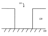
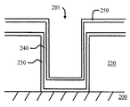
101:ビア
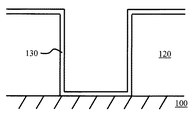
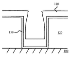
120、220:誘電体層
130、230:拡散バリア層
140:シード層
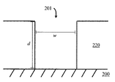
201:高アスペクト比ビア
240:銅シード層
250:ルテニウムシード層
260:銅(Cu)
Claims (18)
- 銅めっきされた高アスペクト比のビアを製造する方法であって、
誘電体層内に高アスペクト比ビアをエッチングするステップと、
前記高アスペクト比ビア内及び前記誘電体層の1つ又は複数の表面の上に拡散バリア層を堆積させるステップと、
前記拡散バリア層の上に銅層を堆積させるステップと、
前記銅層の上にルテニウム層を堆積させるステップと、
前記高アスペクト比ビアを、前記ルテニウム層の上にめっきされた銅で充填するステップと
を含む方法。 - 前記銅は、前記ルテニウム層の上に均一にめっきされる、請求項1に記載の方法。
- 前記銅層は、前記高アスペクト比ビアの張出し及び閉鎖を回避するために、めっき中に通電層として働くのに必要な厚さにまでしか堆積されない、請求項1に記載の方法。
- 化学気相堆積、原子層堆積、蒸着、スパッタリング、溶液ベースの技術、又はスピンオン・コーティングを用いて、前記基板の上に前記誘電体層を堆積させるステップをさらに含む、請求項1に記載の方法。
- 前記高アスペクト比ビアは、反応性イオンエッチングを用いて前記誘電体内にエッチングされる、請求項1に記載の方法。
- 前記高アスペクト比ビアは、5:1以上の深さ対幅のアスペクト比を有する、請求項1に記載の方法。
- 前記拡散バリア層は、化学気相堆積、原子層堆積、又はスパッタリングを用いて堆積される、請求項1に記載の方法。
- 前記銅層は、化学気相堆積、原子層堆積、又はスパッタリングを用いて堆積される、請求項1に記載の方法。
- 前記ルテニウム層は、ルテニウムカルボニル前駆体から化学気相堆積を用いて堆積される、請求項1に記載の方法。
- 電気めっきにより、前記銅がめっきされる、請求項1に記載の方法。
- 前記めっきされた銅、前記ルテニウム層、前記銅層及び前記拡散バリア層を前記誘電体層の上面まで平削りするステップをさらに含む、請求項1に記載の方法。
- 誘電体層内に形成された銅めっきされた高アスペクト比のビアであって、
高アスペクト比ビアと、
前記高アスペクト比ビア及び前記誘電体層の1つ又は複数の表面の内側を覆う拡散バリア層と、
前記拡散バリア層の上の銅層と、
前記銅層の上のルテニウム層と、
前記高アスペクト比ビアを充填し、前記銅めっきされた高アスペクト比ビアを形成する、前記ルテニウム層の上にめっきされた銅と
を含む、銅めっきされた高アスペクト比ビア。 - 前記誘電体層は、二酸化シリコン、シリコン・炭素・酸素・水素材料及び有機ポリマーの1つ又は複数を含む、請求項12に記載の銅めっきされた高アスペクト比ビア。
- 前記誘電体層は、10ナノメートルから1000ナノメートルまでの厚さを有する、請求項12に記載の銅めっきされた高アスペクト比ビア。
- 前記拡散バリア層は窒化タンタルを含む、請求項12に記載の銅めっきされた高アスペクト比ビア。
- 前記拡散バリア層は、0.5ナノメートルから10ナノメートルまでの厚さを有する、請求項12に記載の銅めっきされた高アスペクト比ビア。
- 前記銅層は、1ナノメートルから5ナノメートルまでの厚さを有する、請求項12に記載の銅めっきされた高アスペクト比ビア。
- 前記ルテニウム層は、5ナノメートル以下の厚さを有する、請求項12に記載の銅めっきされた高アスペクト比ビア。
Applications Claiming Priority (1)
| Application Number | Priority Date | Filing Date | Title |
|---|---|---|---|
| US12/163,172 US7964497B2 (en) | 2008-06-27 | 2008-06-27 | Structure to facilitate plating into high aspect ratio vias |
Publications (2)
| Publication Number | Publication Date |
|---|---|
| JP2010010642A true JP2010010642A (ja) | 2010-01-14 |
| JP4536809B2 JP4536809B2 (ja) | 2010-09-01 |
Family
ID=40635481
Family Applications (1)
| Application Number | Title | Priority Date | Filing Date |
|---|---|---|---|
| JP2008268013A Expired - Fee Related JP4536809B2 (ja) | 2008-06-27 | 2008-10-16 | 銅めっきされた高アスペクト比のビア、及びその製造する方法 |
Country Status (5)
| Country | Link |
|---|---|
| US (1) | US7964497B2 (ja) |
| EP (1) | EP2139034A1 (ja) |
| JP (1) | JP4536809B2 (ja) |
| CN (1) | CN101615591A (ja) |
| TW (1) | TW201017821A (ja) |
Cited By (1)
| Publication number | Priority date | Publication date | Assignee | Title |
|---|---|---|---|---|
| JP2019062190A (ja) * | 2017-08-22 | 2019-04-18 | アプライド マテリアルズ インコーポレイテッドApplied Materials,Incorporated | 銅配線のためのシード層 |
Families Citing this family (4)
| Publication number | Priority date | Publication date | Assignee | Title |
|---|---|---|---|---|
| US8661664B2 (en) | 2010-07-19 | 2014-03-04 | International Business Machines Corporation | Techniques for forming narrow copper filled vias having improved conductivity |
| US9748173B1 (en) * | 2016-07-06 | 2017-08-29 | International Business Machines Corporation | Hybrid interconnects and method of forming the same |
| US12322649B2 (en) | 2020-09-11 | 2025-06-03 | Taiwan Semiconductor Manufacturing Co., Ltd. | Interconnect structure of semiconductor device |
| US11527476B2 (en) * | 2020-09-11 | 2022-12-13 | Taiwan Semiconductor Manufacturing Co., Ltd. | Interconnect structure of semiconductor device |
Citations (8)
| Publication number | Priority date | Publication date | Assignee | Title |
|---|---|---|---|---|
| JP2002075994A (ja) * | 2000-08-24 | 2002-03-15 | Matsushita Electric Ind Co Ltd | 半導体装置及びその製造方法 |
| US6790773B1 (en) * | 2002-08-28 | 2004-09-14 | Novellus Systems, Inc. | Process for forming barrier/seed structures for integrated circuits |
| US20050095846A1 (en) * | 2003-10-31 | 2005-05-05 | Basol Bulent M. | System and method for defect free conductor deposition on substrates |
| WO2006057708A2 (en) * | 2004-11-29 | 2006-06-01 | Tokyo Electron Limited | Method and system for measuring a flow rate in a solid precursor delivery system |
| WO2006057706A2 (en) * | 2004-11-23 | 2006-06-01 | Tokyo Electron Limited | Method for deposition of metal layers from metal carbonyl precursors |
| US20060199372A1 (en) * | 2005-03-01 | 2006-09-07 | Applied Materials, Inc. | Reduction of copper dewetting by transition metal deposition |
| WO2006104853A1 (en) * | 2005-03-31 | 2006-10-05 | Tokyo Electron Limited | Low-temperature chemical vapor deposition of low-resistivity ruthenium layers |
| JP2008041700A (ja) * | 2006-08-01 | 2008-02-21 | Tokyo Electron Ltd | 成膜方法、成膜装置及び記憶媒体 |
Family Cites Families (14)
| Publication number | Priority date | Publication date | Assignee | Title |
|---|---|---|---|---|
| KR100249828B1 (ko) | 1997-09-18 | 2000-04-01 | 정선종 | 확산방지막 형성방법 |
| KR100404649B1 (ko) | 1998-02-23 | 2003-11-10 | 가부시끼가이샤 히다치 세이사꾸쇼 | 반도체장치 및 그 제조방법 |
| JP4342075B2 (ja) * | 2000-03-28 | 2009-10-14 | 株式会社東芝 | 半導体装置およびその製造方法 |
| US7010056B1 (en) | 2000-10-10 | 2006-03-07 | Freescale Semiconductor, Inc. | System and method for generating ultra wideband pulses |
| US6403491B1 (en) * | 2000-11-01 | 2002-06-11 | Applied Materials, Inc. | Etch method using a dielectric etch chamber with expanded process window |
| JP4028393B2 (ja) * | 2003-01-09 | 2007-12-26 | 株式会社東芝 | 半導体装置およびその製造方法 |
| US6974768B1 (en) * | 2003-01-15 | 2005-12-13 | Novellus Systems, Inc. | Methods of providing an adhesion layer for adhesion of barrier and/or seed layers to dielectric films |
| US7060619B2 (en) * | 2003-03-04 | 2006-06-13 | Infineon Technologies Ag | Reduction of the shear stress in copper via's in organic interlayer dielectric material |
| US7211508B2 (en) * | 2003-06-18 | 2007-05-01 | Applied Materials, Inc. | Atomic layer deposition of tantalum based barrier materials |
| US7476618B2 (en) | 2004-10-26 | 2009-01-13 | Asm Japan K.K. | Selective formation of metal layers in an integrated circuit |
| FR2890984B1 (fr) | 2005-09-20 | 2009-03-27 | Alchimer Sa | Procede d'electrodeposition destine au revetement d'une surface d'un substrat par un metal. |
| US8222746B2 (en) | 2006-03-03 | 2012-07-17 | Intel Corporation | Noble metal barrier layers |
| US7432195B2 (en) | 2006-03-29 | 2008-10-07 | Tokyo Electron Limited | Method for integrating a conformal ruthenium layer into copper metallization of high aspect ratio features |
| US8258057B2 (en) | 2006-03-30 | 2012-09-04 | Intel Corporation | Copper-filled trench contact for transistor performance improvement |
-
2008
- 2008-06-27 US US12/163,172 patent/US7964497B2/en not_active Expired - Fee Related
- 2008-10-14 EP EP08166587A patent/EP2139034A1/en not_active Withdrawn
- 2008-10-16 JP JP2008268013A patent/JP4536809B2/ja not_active Expired - Fee Related
-
2009
- 2009-06-23 CN CN200910150840A patent/CN101615591A/zh active Pending
- 2009-06-24 TW TW098121240A patent/TW201017821A/zh unknown
Patent Citations (8)
| Publication number | Priority date | Publication date | Assignee | Title |
|---|---|---|---|---|
| JP2002075994A (ja) * | 2000-08-24 | 2002-03-15 | Matsushita Electric Ind Co Ltd | 半導体装置及びその製造方法 |
| US6790773B1 (en) * | 2002-08-28 | 2004-09-14 | Novellus Systems, Inc. | Process for forming barrier/seed structures for integrated circuits |
| US20050095846A1 (en) * | 2003-10-31 | 2005-05-05 | Basol Bulent M. | System and method for defect free conductor deposition on substrates |
| WO2006057706A2 (en) * | 2004-11-23 | 2006-06-01 | Tokyo Electron Limited | Method for deposition of metal layers from metal carbonyl precursors |
| WO2006057708A2 (en) * | 2004-11-29 | 2006-06-01 | Tokyo Electron Limited | Method and system for measuring a flow rate in a solid precursor delivery system |
| US20060199372A1 (en) * | 2005-03-01 | 2006-09-07 | Applied Materials, Inc. | Reduction of copper dewetting by transition metal deposition |
| WO2006104853A1 (en) * | 2005-03-31 | 2006-10-05 | Tokyo Electron Limited | Low-temperature chemical vapor deposition of low-resistivity ruthenium layers |
| JP2008041700A (ja) * | 2006-08-01 | 2008-02-21 | Tokyo Electron Ltd | 成膜方法、成膜装置及び記憶媒体 |
Cited By (2)
| Publication number | Priority date | Publication date | Assignee | Title |
|---|---|---|---|---|
| JP2019062190A (ja) * | 2017-08-22 | 2019-04-18 | アプライド マテリアルズ インコーポレイテッドApplied Materials,Incorporated | 銅配線のためのシード層 |
| JP2023182638A (ja) * | 2017-08-22 | 2023-12-26 | アプライド マテリアルズ インコーポレイテッド | 銅配線のためのシード層 |
Also Published As
| Publication number | Publication date |
|---|---|
| CN101615591A (zh) | 2009-12-30 |
| JP4536809B2 (ja) | 2010-09-01 |
| EP2139034A1 (en) | 2009-12-30 |
| TW201017821A (en) | 2010-05-01 |
| US7964497B2 (en) | 2011-06-21 |
| US20090321933A1 (en) | 2009-12-31 |
Similar Documents
| Publication | Publication Date | Title |
|---|---|---|
| US8698318B2 (en) | Superfilled metal contact vias for semiconductor devices | |
| US7915162B2 (en) | Method of forming damascene filament wires | |
| US7521358B2 (en) | Process integration scheme to lower overall dielectric constant in BEoL interconnect structures | |
| TWI406361B (zh) | 於互連應用中形成可靠介層接觸之結構及方法 | |
| CN101150112B (zh) | 半导体器件及其制造方法 | |
| US8058164B2 (en) | Methods of fabricating electronic devices using direct copper plating | |
| US9343407B2 (en) | Method to fabricate copper wiring structures and structures formed thereby | |
| JP7027432B2 (ja) | 相互接続構造及びその形成方法 | |
| KR20170066297A (ko) | 상호접속 구조물 및 상호접속 구조물의 형성 방법 | |
| TWI513378B (zh) | 改善窄銅填孔之導電性的方法及結構 | |
| JP4536809B2 (ja) | 銅めっきされた高アスペクト比のビア、及びその製造する方法 | |
| US8084355B2 (en) | Methods of forming copper-comprising conductive lines in the fabrication of integrated circuitry | |
| JP2005252193A (ja) | 配線構造の形成方法及び半導体装置 | |
| CN102446811B (zh) | 金属互连结构及金属层间通孔和互连金属线的形成方法 | |
| US20070264815A1 (en) | Method for fabricating semiconductor device | |
| JP5362029B2 (ja) | 半導体装置の製造方法 | |
| KR100772252B1 (ko) | 구리 배선의 제조 방법 | |
| KR20070052452A (ko) | 반도체 소자의 금속배선 제조방법 | |
| JP2004014816A (ja) | 半導体製造方法および半導体装置 | |
| CN110890317A (zh) | 半导体器件及其制备方法 | |
| KR20060114215A (ko) | 반도체 소자의 금속 배선 형성 방법 | |
| KR20050118465A (ko) | 반도체 소자의 금속배선 형성 방법 |
Legal Events
| Date | Code | Title | Description |
|---|---|---|---|
| A521 | Request for written amendment filed |
Free format text: JAPANESE INTERMEDIATE CODE: A523 Effective date: 20091016 Free format text: JAPANESE INTERMEDIATE CODE: A821 Effective date: 20090924 |
|
| A02 | Decision of refusal |
Free format text: JAPANESE INTERMEDIATE CODE: A02 Effective date: 20091110 |
|
| A521 | Request for written amendment filed |
Free format text: JAPANESE INTERMEDIATE CODE: A523 Effective date: 20100303 |
|
| A911 | Transfer to examiner for re-examination before appeal (zenchi) |
Free format text: JAPANESE INTERMEDIATE CODE: A911 Effective date: 20100330 |
|
| TRDD | Decision of grant or rejection written | ||
| A01 | Written decision to grant a patent or to grant a registration (utility model) |
Free format text: JAPANESE INTERMEDIATE CODE: A01 Effective date: 20100608 |
|
| RD14 | Notification of resignation of power of sub attorney |
Free format text: JAPANESE INTERMEDIATE CODE: A7434 Effective date: 20100608 |
|
| A01 | Written decision to grant a patent or to grant a registration (utility model) |
Free format text: JAPANESE INTERMEDIATE CODE: A01 |
|
| A61 | First payment of annual fees (during grant procedure) |
Free format text: JAPANESE INTERMEDIATE CODE: A61 Effective date: 20100616 |
|
| FPAY | Renewal fee payment (event date is renewal date of database) |
Free format text: PAYMENT UNTIL: 20130625 Year of fee payment: 3 |
|
| R150 | Certificate of patent or registration of utility model |
Free format text: JAPANESE INTERMEDIATE CODE: R150 |
|
| R250 | Receipt of annual fees |
Free format text: JAPANESE INTERMEDIATE CODE: R250 |
|
| R250 | Receipt of annual fees |
Free format text: JAPANESE INTERMEDIATE CODE: R250 |
|
| LAPS | Cancellation because of no payment of annual fees |