JP2010010642A - Copper-plated via of high aspect ratio, and its manufacturing method - Google Patents
Copper-plated via of high aspect ratio, and its manufacturing method Download PDFInfo
- Publication number
- JP2010010642A JP2010010642A JP2008268013A JP2008268013A JP2010010642A JP 2010010642 A JP2010010642 A JP 2010010642A JP 2008268013 A JP2008268013 A JP 2008268013A JP 2008268013 A JP2008268013 A JP 2008268013A JP 2010010642 A JP2010010642 A JP 2010010642A
- Authority
- JP
- Japan
- Prior art keywords
- layer
- aspect ratio
- high aspect
- copper
- ratio via
- Prior art date
- Legal status (The legal status is an assumption and is not a legal conclusion. Google has not performed a legal analysis and makes no representation as to the accuracy of the status listed.)
- Granted
Links
Images


Classifications
-
- H—ELECTRICITY
- H01—ELECTRIC ELEMENTS
- H01L—SEMICONDUCTOR DEVICES NOT COVERED BY CLASS H10
- H01L21/00—Processes or apparatus adapted for the manufacture or treatment of semiconductor or solid state devices or of parts thereof
- H01L21/70—Manufacture or treatment of devices consisting of a plurality of solid state components formed in or on a common substrate or of parts thereof; Manufacture of integrated circuit devices or of parts thereof
- H01L21/71—Manufacture of specific parts of devices defined in group H01L21/70
- H01L21/768—Applying interconnections to be used for carrying current between separate components within a device comprising conductors and dielectrics
- H01L21/76838—Applying interconnections to be used for carrying current between separate components within a device comprising conductors and dielectrics characterised by the formation and the after-treatment of the conductors
- H01L21/76841—Barrier, adhesion or liner layers
- H01L21/76843—Barrier, adhesion or liner layers formed in openings in a dielectric
-
- H—ELECTRICITY
- H01—ELECTRIC ELEMENTS
- H01L—SEMICONDUCTOR DEVICES NOT COVERED BY CLASS H10
- H01L21/00—Processes or apparatus adapted for the manufacture or treatment of semiconductor or solid state devices or of parts thereof
- H01L21/70—Manufacture or treatment of devices consisting of a plurality of solid state components formed in or on a common substrate or of parts thereof; Manufacture of integrated circuit devices or of parts thereof
- H01L21/71—Manufacture of specific parts of devices defined in group H01L21/70
- H01L21/768—Applying interconnections to be used for carrying current between separate components within a device comprising conductors and dielectrics
- H01L21/76838—Applying interconnections to be used for carrying current between separate components within a device comprising conductors and dielectrics characterised by the formation and the after-treatment of the conductors
- H01L21/76841—Barrier, adhesion or liner layers
- H01L21/76871—Layers specifically deposited to enhance or enable the nucleation of further layers, i.e. seed layers
- H01L21/76873—Layers specifically deposited to enhance or enable the nucleation of further layers, i.e. seed layers for electroplating
-
- H—ELECTRICITY
- H01—ELECTRIC ELEMENTS
- H01L—SEMICONDUCTOR DEVICES NOT COVERED BY CLASS H10
- H01L23/00—Details of semiconductor or other solid state devices
- H01L23/52—Arrangements for conducting electric current within the device in operation from one component to another, i.e. interconnections, e.g. wires, lead frames
- H01L23/522—Arrangements for conducting electric current within the device in operation from one component to another, i.e. interconnections, e.g. wires, lead frames including external interconnections consisting of a multilayer structure of conductive and insulating layers inseparably formed on the semiconductor body
- H01L23/532—Arrangements for conducting electric current within the device in operation from one component to another, i.e. interconnections, e.g. wires, lead frames including external interconnections consisting of a multilayer structure of conductive and insulating layers inseparably formed on the semiconductor body characterised by the materials
- H01L23/53204—Conductive materials
- H01L23/53209—Conductive materials based on metals, e.g. alloys, metal silicides
- H01L23/53228—Conductive materials based on metals, e.g. alloys, metal silicides the principal metal being copper
- H01L23/53238—Additional layers associated with copper layers, e.g. adhesion, barrier, cladding layers
-
- H—ELECTRICITY
- H01—ELECTRIC ELEMENTS
- H01L—SEMICONDUCTOR DEVICES NOT COVERED BY CLASS H10
- H01L2221/00—Processes or apparatus adapted for the manufacture or treatment of semiconductor or solid state devices or of parts thereof covered by H01L21/00
- H01L2221/10—Applying interconnections to be used for carrying current between separate components within a device
- H01L2221/1068—Formation and after-treatment of conductors
- H01L2221/1073—Barrier, adhesion or liner layers
- H01L2221/1084—Layers specifically deposited to enhance or enable the nucleation of further layers, i.e. seed layers
- H01L2221/1089—Stacks of seed layers
-
- H—ELECTRICITY
- H01—ELECTRIC ELEMENTS
- H01L—SEMICONDUCTOR DEVICES NOT COVERED BY CLASS H10
- H01L2924/00—Indexing scheme for arrangements or methods for connecting or disconnecting semiconductor or solid-state bodies as covered by H01L24/00
- H01L2924/0001—Technical content checked by a classifier
- H01L2924/0002—Not covered by any one of groups H01L24/00, H01L24/00 and H01L2224/00
Abstract
Description
本発明は、半導体相互接続構造体に関し、より具体的には、改善された高アスペクト比のビア及びそれを形成するための技術に関する。 The present invention relates to semiconductor interconnect structures, and more particularly to improved high aspect ratio vias and techniques for forming the same.
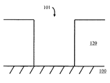
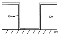
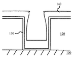
多層の配線アレイ構造部(feature)の寸法が縮小し続けるに従って、ビアの製造はますます困難になってきている。すなわち、従来のビア製造のプロセスは、現在のところ望ましいスケーリングされた構造部の寸法に追いつくことができない。例えば、図1−図3は、より小さい構造部の寸法(例えば、45ナノメートル(nm)のノード又はそれより小さい技術)に関係するときの、従来のビア製造プロセスと関連した一般的な問題を示す。図1に示されるように、基板100の上に誘電体層120が堆積され、誘電体層120内にビア101がエッチングされる。図2に示されるように、ビア101/誘電体120の表面は、拡散バリア層130で内側が覆われる(ライニングされる)。拡散バリア層は、窒化タンタル(TaN)又は他の任意の好適な拡散バリア材料とすることができる。ビア101を銅(Cu)で充填するために、電気めっきが用いられる。しかしながら、電気めっきを行うためには、まず、後でCuをめっきすることができるシード層を堆積させることが必要である。すなわち、図3に示されるように、拡散バリア層130の上にCuをスパッタ堆積させることによって、シード層140が形成される。
As the dimensions of multi-layer wiring array features continue to shrink, via fabrication becomes increasingly difficult. That is, conventional via manufacturing processes cannot keep up with the currently desired scaled structure dimensions. For example, FIGS. 1-3 illustrate general issues associated with conventional via fabrication processes when related to smaller structure dimensions (eg, 45 nanometer (nm) node or smaller technology). Indicates. As shown in FIG. 1, a
この手法に関連する問題は、ビアの幅が約80nm未満にまで縮小し、アスペクト(深さ/幅)比が約5:1より大きくなると、構造体の電気めっきが破損し始めることである。図3に示されるように、シード層140におけるCuの厚さは、実質的に不均一である。この不均一性は、めっきすることができない箇所がないことを確実にするために、ビア底部/側壁上に、連続的にするのに十分な厚さをもつCuの層が必要であるという事実に加えて、スパッタ堆積プロセスの方向性をもつ性質によって生じた結果である。その結果、ビアの水平面上に、過剰な量のCuが堆積される。この過剰なCuは、最後にはビア開口部に張り出すことになる。結果として、電気めっきを試みたとき、この張出し部がビア開口部をふさぎ、ビア開口部が閉鎖し、ビアの内部に充填されていないボイドが残り、そのことが破局的な故障となる。
The problem associated with this approach is that the electroplating of the structure begins to break when the via width is reduced to less than about 80 nm and the aspect (depth / width) ratio is greater than about 5: 1. As shown in FIG. 3, the Cu thickness in the
上述の張出し部が閉鎖する問題を防ぐために、拡散バリア層の上にCuシード層をスパッタ堆積させる代わりに、化学気相堆積(CVD)によって、すなわち、過剰なCOの存在下でルテニウムカルボニル(Ru3(CO)12)前駆体から、拡散バリア層の上にルテニウム(Ru)シード層を堆積させる、代替的な手法が考え出された。この方法で生成されるRuシード層は、共形に(conformally)堆積させることが可能であり、よって、厚い張出し層が生成されず、そのため、後のCu電気めっきステップにおいてボイドが形成される問題が大きく減少する。 To prevent the overhang problem described above, instead of sputter depositing a Cu seed layer on the diffusion barrier layer, ruthenium carbonyl (Ru) by chemical vapor deposition (CVD), ie in the presence of excess CO. An alternative approach has been devised that deposits a ruthenium (Ru) seed layer over a diffusion barrier layer from a 3 (CO) 12 ) precursor. The Ru seed layer produced in this way can be conformally deposited, so that a thick overhang layer is not produced and therefore voids are formed in a subsequent Cu electroplating step. Is greatly reduced.
しかしながら、Ruシード層の使用は、Cuと比べてRuの抵抗率が相対的に高いことと、Ruの化学的不活性とから生じる重大な欠点を有する。例えば、ビア金属を誘電体表面まで平削りするために、典型的には、電気めっきに続いて化学機械研磨(CMP)が用いられる。実際問題として、5nmは、標準的なCu研磨スラリーを用いて研磨により除去できる、Ruの量のほぼ上限値である。しかしながら、Ruのバルク抵抗率は、Cuのものより4倍以上高い。ウェハの両端にかかる電圧の降下が、Cu堆積において容認できない不均一性をもたらすので、5nmのRuしか堆積されない場合、結果として得られる構造体の抵抗率が、電気めっきを極めて困難にする。より厚いRu層を堆積させることによって基板の導電率を増大させ、この問題を軽減させることができるが、後のCMPプロセスは不可能である。問題の選択を後に残し、めっきを容易にするようにRuが十分に厚い場合、標準的なCu研磨スラリーを用いて引き続きCMPを行うことができない。CMPが可能になるところまでRu層を薄層化した場合、標準的な技術を用いて均一にめっきするには、基板の抵抗が大きすぎる。さらに、より厚いRu層を研磨するための方法が開発されたとしても、それは望ましい解決法ではない。CMPの後、電気めっきプロセスを容易にするために添加される付加的なRuがビア内に残り、それにより、ビア内で利用可能なCuの量が減少し、ビアの抵抗率が著しく増大し、性能が低下することになる。 However, the use of a Ru seed layer has significant drawbacks arising from the relatively high resistivity of Ru compared to Cu and the chemical inertness of Ru. For example, chemical mechanical polishing (CMP) is typically used following electroplating to plan via metal to the dielectric surface. In practice, 5 nm is an approximately upper limit on the amount of Ru that can be removed by polishing using a standard Cu polishing slurry. However, the bulk resistivity of Ru is more than four times higher than that of Cu. Since the voltage drop across the wafer results in unacceptable non-uniformities in Cu deposition, if only 5 nm of Ru is deposited, the resulting structure resistivity makes electroplating very difficult. Depositing a thicker Ru layer can increase the conductivity of the substrate and alleviate this problem, but a later CMP process is not possible. If Ru remains sufficiently thick to leave the problem choice behind and facilitate plating, subsequent CMP cannot be performed using a standard Cu polishing slurry. When the Ru layer is thinned to the point where CMP is possible, the resistance of the substrate is too high for uniform plating using standard techniques. Furthermore, even if a method for polishing thicker Ru layers is developed, it is not a desirable solution. After CMP, additional Ru added to facilitate the electroplating process remains in the via, thereby reducing the amount of Cu available in the via and significantly increasing the via resistivity. The performance will be reduced.
従って、最新のスケーリング技術の要件に適応することができ、適切に機能する実行可能なビアを一貫して生成できる、改善されたビア製造プロセスが必要とされる。 Therefore, there is a need for an improved via manufacturing process that can adapt to the requirements of modern scaling techniques and consistently generate well-functioning workable vias.
本発明は、改善された高アスペクト比のビア及びそれを形成するための技術を提供する。本発明の1つの態様において、銅めっきされた高アスペクト比ビアを製造する方法が提供される。この方法は以下のステップを含む。誘電体層内に、高アスペクト比ビアをエッチングする。高アスペクト比ビア内及び誘電体層の1つ又は複数の表面の上に拡散バリア層を堆積させる。拡散バリア層の上に銅層を堆積させる。銅層の上にルテニウム層を堆積させる。高アスペクト比ビアを、ルテニウム層の上にめっきされた銅で充填する。 The present invention provides an improved high aspect ratio via and techniques for forming it. In one aspect of the present invention, a method for producing a copper plated high aspect ratio via is provided. The method includes the following steps. Etch high aspect ratio vias in the dielectric layer. A diffusion barrier layer is deposited in the high aspect ratio via and on one or more surfaces of the dielectric layer. A copper layer is deposited over the diffusion barrier layer. A ruthenium layer is deposited on the copper layer. High aspect ratio vias are filled with copper plated on the ruthenium layer.
本発明の別の態様において、誘電体層内に形成された銅めっきされた高アスペクト比ビアが提供される。銅めっきされた高アスペクト比ビアは、高アスペクト比ビアと、高アスペクト比ビア及び誘電体層の1つ又は複数の表面の内側を覆う拡散バリア層と、拡散バリア層の上の銅層と、銅層の上のルテニウム層と、高アスペクト比ビアを充填し、銅めっきされた高アスペクト比ビアを形成する、ルテニウム層の上にめっきされた銅とを含む。 In another aspect of the present invention, a copper plated high aspect ratio via formed in a dielectric layer is provided. The copper plated high aspect ratio via includes a high aspect ratio via, a diffusion barrier layer that covers the inside of one or more surfaces of the high aspect ratio via and the dielectric layer, a copper layer over the diffusion barrier layer, A ruthenium layer overlying the copper layer, and copper plated over the ruthenium layer filling the high aspect ratio via and forming a copper plated high aspect ratio via.
本発明のより完全な理解、並びに、本発明のさらなる特徴及び利点が、以下の詳細な説明及び図面を参照することによって得られるであろう。 A more complete understanding of the present invention, as well as further features and advantages of the present invention, will be obtained by reference to the following detailed description and drawings.
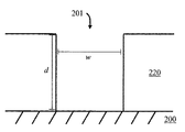
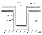
図4−図7は、例示的なビア製造プロセスを示す断面図である。図4に示されるように、基板200の上に誘電体層220が堆積される。誘電体層220は、これらに限られるものではないが、二酸化シリコン(SiO2)、シリコン−炭素−酸素−水素材料(例えば、SICOH)及び有機ポリマーの1つ又は複数を含む任意の好適な誘電体材料を含むことができ、化学気相堆積(CVD)、原子層堆積(ALD)、蒸着、スパッタリング、又はスピンオン・コーティングといった溶液ベースの技術のような任意の好適な堆積プロセスを用いて、約10ナノメートル(nm)から約1000nmの厚さまで堆積させることができる。基板200は、通常、単一又は多層の配線アレイ内に何らかの配線又はコンタクト層を示す。次に、反応性イオンエッチング(RIE)などの任意の好適なエッチング・プロセスを用いて、誘電体層220内に高アスペクト比のビア201がエッチングされる。1つの例示的な実施形態によると、高アスペクト比のビア201は、RIEを用いて誘電体層220内にエッチングされ、約5:1以上の深さd/幅wのアスペクト比を有する。
4-7 are cross-sectional views illustrating an exemplary via manufacturing process. As shown in FIG. 4, a
図5に示されるように、拡散バリア層230が、高アスペクト比ビア201/誘電体層220の上面の内側を覆う。拡散バリア層230は、これらに限られるものではないが、窒化タンタル(TaN)、或いは他の金属窒化物、酸化物、硫化物、ホウ化物、又はリン化物を含む任意の好適な拡散バリア材料を含むことができ、CVD、ALD又はスパッタリングのような任意の好適な堆積プロセスを用いて、高アスペクト比のビア201内/誘電体層220の上面の上に、約0.5nmから約10nmの厚さまで堆積させることができる。
As shown in FIG. 5, the
図6に示されるように、拡散バリア層230の上に、銅(Cu)シード層240が堆積される。Cuシード層240は、CVD、ALD又はスパッタリングのような任意の好適な堆積プロセスを用いて、約1nmから約5nmの厚さまで堆積させることができる。Cuシード層240は、電気めっき中、主として通電層(current carrying layer)として堆積されるため、(例えば、上述の図1−図3に表されるプロセスと比べると)ビアの側壁上に連続的に被覆するのに必要とされる厚さを有する必要はない(すなわち、Cuシード層240は、電気めっき中、通電層として働くのに必要な厚さを有することだけを必要とする、すぐ上に提供された例示的な厚さを参照されたい)。従って、張出し部(上述の)は存在せず(閉鎖及び充填されていないボイドを防ぐ)、そのことは、より小さくより高いアスペクト比の構造体に対するめっきの拡張性を容易にする。
As shown in FIG. 6, a copper (Cu)
次に、Cuシード層240の上に、ルテニウム(Ru)シード層250が堆積される。Ruシード層250は、CVD又はALDなどの任意の好適な堆積プロセスを用いて堆積させることができる。例示的な実施形態によると、Ruシード層250は、CVDを用いて堆積される、すなわち、過剰なCOの存在下でルテニウムカルボニル(Ru3(CO)12)前駆体から堆積される。有利なことに、この高度に共形のプロセスによって形成されたRuシード層250は、ビアの側壁上の連続的な被覆を確実にする厚さまでしか堆積されず、よって、標準的な化学機械研磨(CMP)によって設定される制限値の範囲内にある(下記の図7の説明を参照されたい)。例示的な実施形態によると、Ruシード層250は、約5nm以下の厚さまで堆積される。Cuシード層240の上のRuシード層250は、ここではRu・オン・Cu二重層とも呼ばれる。
Next, a ruthenium (Ru)
図7に示されるように、例えば、Cu260をRuシード層250の上に電気めっきすることによって、高アスペクト比ビア201がCu260で充填され、Cuめっきされた高アスペクト比のビアを形成する。必要に応じて、次に、CMPを用いて、めっきされたCu260/Ruシード層250/Cuシード層240/拡散バリア層230を、誘電体層220(図示せず)の上面まで平削りすることができる。
As shown in FIG. 7, for example, by electroplating
本Ru−オン−Cu二重層のシード層構成の1つの利点(Cuの電気めっきに関する、上記参照)は、Ruの上にめっきされたCuが、例えば、Cuシード層上にめっきされたCuと比べて、優れた形態(morphology)を示すことである。すなわち、ラインにおいて、より大きい粒子が観察され、ビアにおいて、より大きい配向された柱状粒子が見出される。より大きい粒子は導電率を改善し、よって、ビアの性能を改善する。 One advantage of the present Ru-on-Cu bilayer seed layer configuration (see above for Cu electroplating) is that Cu plated on Ru, for example, Cu plated on a Cu seed layer In comparison, it shows an excellent morphology. That is, larger particles are observed in the lines and larger oriented columnar particles are found in the vias. Larger particles improve electrical conductivity and thus improve via performance.
同様に二重層のシード層を含む従来のビア製造技術は、Cu−オン−Ru構成を用いていた。しかしながら、このCu−オン−Ru構成は、本Ru−オン−Cu二重層構成に比べて幾つかの注目すべき不利な点を有する。すなわち、上述のように、Cu−オン−Ru構成は、Ruの上のCuめっきと関連した形態上の利点を提供するものではない。さらに、本Ru−オン−Cu二重層構成を用いる場合、二重層のCu成分は、Cu−オン−Ru構成におけるより薄く作製することができ、依然としてめっきを実行できるままである。 Similarly, conventional via fabrication techniques that include a double seed layer used a Cu-on-Ru configuration. However, this Cu-on-Ru configuration has several notable disadvantages compared to the present Ru-on-Cu bilayer configuration. That is, as noted above, the Cu-on-Ru configuration does not provide the morphological advantages associated with Cu plating on Ru. Furthermore, when using the present Ru-on-Cu bilayer configuration, the Cu component of the bilayer can be made thinner than in the Cu-on-Ru configuration and still remain capable of plating.
ほんの一例として、それぞれ3nmのCu上に1nmのRu、1nmのRu上に3nmのCuを有する、Ru−オン−Cu及びCu−オン−Ruシード層の両方が、同一のビア構造体上に生成された。同一のめっき条件を用いたとき、Ru−オン−Cuのサンプルはうまくめっきされ(すなわち、均一なめっき)、Cu−オン−Ruのサンプルはうまくめっきされないことが分かった。Cu−オン−Ruのサンプルのめっきは、基板の導電率が不十分であることに関連した全体の不均一性のタイプを示した。 By way of example only, both Ru-on-Cu and Cu-on-Ru seed layers are produced on the same via structure, each with 1 nm Ru on 3 nm Cu and 3 nm Cu on 1 nm Ru. It was done. It was found that when using the same plating conditions, the Ru-on-Cu sample was well plated (ie, uniform plating) and the Cu-on-Ru sample was not well plated. The plating of the Cu-on-Ru sample showed an overall non-uniformity type associated with insufficient substrate conductivity.
これらのサンプルにおける相違は、2つのシード層が大気に曝されたときに受ける酸化の程度が異なることに起因する。貴金属であるRuは、Cuと比べてあまり酸化の影響を受けやすくない。Ru−オン−Cu構造体においては、Cuは、その上にあるRu層によって酸化から保護されるが、Cu−オン−Ru構造体においては、Cuは、大気に直接曝される。Cuの酸化は、Cu−オン−Ruシード層の導電率を低減させ、めっきをより困難にする。めっき浴中でCu酸化物の著しい溶解が生じることがあり、基板の導電率に対して同様の有害な結果を有する。 The difference in these samples is due to the different degrees of oxidation experienced when the two seed layers are exposed to the atmosphere. Ru, which is a noble metal, is less susceptible to oxidation than Cu. In the Ru-on-Cu structure, Cu is protected from oxidation by the overlying Ru layer, but in the Cu-on-Ru structure, Cu is directly exposed to the atmosphere. Cu oxidation reduces the conductivity of the Cu-on-Ru seed layer and makes plating more difficult. Significant dissolution of Cu oxide can occur in the plating bath, with similar deleterious consequences for substrate conductivity.
Ru−オン−Cu二重層構成の別の利点は、拡散バリア層230がTaNを含むとき(上記参照)、Cu/TaN界面が結果として生じることである(すなわち、Ru−オン−Cu二重層シード層と拡散バリア層との間に)。Cu/TaN界面は、広範にわたって試験され、従来のシステムにおいて日常的に使用されてきた。
Another advantage of the Ru-on-Cu bilayer configuration is that when the
本発明の例証となる実施形態がここに説明されるが、本発明は、それらの正確な実施形態に制限されるものではないこと、及び、当業者であれば本発明の範囲から逸脱することなく種々の他の変更及び修正をなし得ることを理解すべきである。 Illustrative embodiments of the invention are described herein, but the invention is not limited to those precise embodiments and those skilled in the art will depart from the scope of the invention. It should be understood that various other changes and modifications may be made.
100、200:基板
101:ビア
120、220:誘電体層
130、230:拡散バリア層
140:シード層
201:高アスペクト比ビア
240:銅シード層
250:ルテニウムシード層
260:銅(Cu)
100, 200: Substrate 101:
Claims (18)
誘電体層内に高アスペクト比ビアをエッチングするステップと、
前記高アスペクト比ビア内及び前記誘電体層の1つ又は複数の表面の上に拡散バリア層を堆積させるステップと、
前記拡散バリア層の上に銅層を堆積させるステップと、
前記銅層の上にルテニウム層を堆積させるステップと、
前記高アスペクト比ビアを、前記ルテニウム層の上にめっきされた銅で充填するステップと
を含む方法。 A method for producing a copper plated high aspect ratio via comprising:
Etching high aspect ratio vias in the dielectric layer;
Depositing a diffusion barrier layer in the high aspect ratio via and on one or more surfaces of the dielectric layer;
Depositing a copper layer on the diffusion barrier layer;
Depositing a ruthenium layer on the copper layer;
Filling the high aspect ratio via with copper plated on the ruthenium layer.
高アスペクト比ビアと、
前記高アスペクト比ビア及び前記誘電体層の1つ又は複数の表面の内側を覆う拡散バリア層と、
前記拡散バリア層の上の銅層と、
前記銅層の上のルテニウム層と、
前記高アスペクト比ビアを充填し、前記銅めっきされた高アスペクト比ビアを形成する、前記ルテニウム層の上にめっきされた銅と
を含む、銅めっきされた高アスペクト比ビア。 A copper plated high aspect ratio via formed in a dielectric layer comprising:
High aspect ratio vias,
A diffusion barrier layer overlying one or more surfaces of the high aspect ratio via and the dielectric layer;
A copper layer over the diffusion barrier layer;
A ruthenium layer on the copper layer;
A copper plated high aspect ratio via comprising filling the high aspect ratio via and copper plated on the ruthenium layer to form the copper plated high aspect ratio via.
Applications Claiming Priority (1)
| Application Number | Priority Date | Filing Date | Title |
|---|---|---|---|
| US12/163,172 US7964497B2 (en) | 2008-06-27 | 2008-06-27 | Structure to facilitate plating into high aspect ratio vias |
Publications (2)
| Publication Number | Publication Date |
|---|---|
| JP2010010642A true JP2010010642A (en) | 2010-01-14 |
| JP4536809B2 JP4536809B2 (en) | 2010-09-01 |
Family
ID=40635481
Family Applications (1)
| Application Number | Title | Priority Date | Filing Date |
|---|---|---|---|
| JP2008268013A Expired - Fee Related JP4536809B2 (en) | 2008-06-27 | 2008-10-16 | Copper plated high aspect ratio vias and methods of manufacturing the same |
Country Status (5)
| Country | Link |
|---|---|
| US (1) | US7964497B2 (en) |
| EP (1) | EP2139034A1 (en) |
| JP (1) | JP4536809B2 (en) |
| CN (1) | CN101615591A (en) |
| TW (1) | TW201017821A (en) |
Cited By (1)
| Publication number | Priority date | Publication date | Assignee | Title |
|---|---|---|---|---|
| JP2019062190A (en) * | 2017-08-22 | 2019-04-18 | アプライド マテリアルズ インコーポレイテッドApplied Materials,Incorporated | Seed layers for copper interconnects |
Families Citing this family (3)
| Publication number | Priority date | Publication date | Assignee | Title |
|---|---|---|---|---|
| US8661664B2 (en) | 2010-07-19 | 2014-03-04 | International Business Machines Corporation | Techniques for forming narrow copper filled vias having improved conductivity |
| US9748173B1 (en) * | 2016-07-06 | 2017-08-29 | International Business Machines Corporation | Hybrid interconnects and method of forming the same |
| US11527476B2 (en) * | 2020-09-11 | 2022-12-13 | Taiwan Semiconductor Manufacturing Co., Ltd. | Interconnect structure of semiconductor device |
Citations (8)
| Publication number | Priority date | Publication date | Assignee | Title |
|---|---|---|---|---|
| JP2002075994A (en) * | 2000-08-24 | 2002-03-15 | Matsushita Electric Ind Co Ltd | Semiconductor device and its manufacturing method |
| US6790773B1 (en) * | 2002-08-28 | 2004-09-14 | Novellus Systems, Inc. | Process for forming barrier/seed structures for integrated circuits |
| US20050095846A1 (en) * | 2003-10-31 | 2005-05-05 | Basol Bulent M. | System and method for defect free conductor deposition on substrates |
| WO2006057708A2 (en) * | 2004-11-29 | 2006-06-01 | Tokyo Electron Limited | Method and system for measuring a flow rate in a solid precursor delivery system |
| WO2006057706A2 (en) * | 2004-11-23 | 2006-06-01 | Tokyo Electron Limited | Method for deposition of metal layers from metal carbonyl precursors |
| US20060199372A1 (en) * | 2005-03-01 | 2006-09-07 | Applied Materials, Inc. | Reduction of copper dewetting by transition metal deposition |
| WO2006104853A1 (en) * | 2005-03-31 | 2006-10-05 | Tokyo Electron Limited | Low-temperature chemical vapor deposition of low-resistivity ruthenium layers |
| JP2008041700A (en) * | 2006-08-01 | 2008-02-21 | Tokyo Electron Ltd | Method and apparatus of forming film, and recording medium |
Family Cites Families (14)
| Publication number | Priority date | Publication date | Assignee | Title |
|---|---|---|---|---|
| KR100249828B1 (en) | 1997-09-18 | 2000-04-01 | 정선종 | The coating method for preventing diffusion |
| KR100404649B1 (en) | 1998-02-23 | 2003-11-10 | 가부시끼가이샤 히다치 세이사꾸쇼 | Semiconductor device and fabrication method thereof |
| JP4342075B2 (en) * | 2000-03-28 | 2009-10-14 | 株式会社東芝 | Semiconductor device and manufacturing method thereof |
| US7010056B1 (en) | 2000-10-10 | 2006-03-07 | Freescale Semiconductor, Inc. | System and method for generating ultra wideband pulses |
| US6403491B1 (en) * | 2000-11-01 | 2002-06-11 | Applied Materials, Inc. | Etch method using a dielectric etch chamber with expanded process window |
| JP4028393B2 (en) * | 2003-01-09 | 2007-12-26 | 株式会社東芝 | Semiconductor device and manufacturing method thereof |
| US6974768B1 (en) * | 2003-01-15 | 2005-12-13 | Novellus Systems, Inc. | Methods of providing an adhesion layer for adhesion of barrier and/or seed layers to dielectric films |
| US7060619B2 (en) * | 2003-03-04 | 2006-06-13 | Infineon Technologies Ag | Reduction of the shear stress in copper via's in organic interlayer dielectric material |
| KR20060079144A (en) * | 2003-06-18 | 2006-07-05 | 어플라이드 머티어리얼스, 인코포레이티드 | Atomic layer deposition of barrier materials |
| US7476618B2 (en) | 2004-10-26 | 2009-01-13 | Asm Japan K.K. | Selective formation of metal layers in an integrated circuit |
| FR2890984B1 (en) | 2005-09-20 | 2009-03-27 | Alchimer Sa | ELECTRODEPOSITION PROCESS FOR COATING A SURFACE OF A SUBSTRATE WITH A METAL |
| US8222746B2 (en) | 2006-03-03 | 2012-07-17 | Intel Corporation | Noble metal barrier layers |
| US7432195B2 (en) | 2006-03-29 | 2008-10-07 | Tokyo Electron Limited | Method for integrating a conformal ruthenium layer into copper metallization of high aspect ratio features |
| US8258057B2 (en) | 2006-03-30 | 2012-09-04 | Intel Corporation | Copper-filled trench contact for transistor performance improvement |
-
2008
- 2008-06-27 US US12/163,172 patent/US7964497B2/en not_active Expired - Fee Related
- 2008-10-14 EP EP08166587A patent/EP2139034A1/en not_active Withdrawn
- 2008-10-16 JP JP2008268013A patent/JP4536809B2/en not_active Expired - Fee Related
-
2009
- 2009-06-23 CN CN200910150840A patent/CN101615591A/en active Pending
- 2009-06-24 TW TW098121240A patent/TW201017821A/en unknown
Patent Citations (8)
| Publication number | Priority date | Publication date | Assignee | Title |
|---|---|---|---|---|
| JP2002075994A (en) * | 2000-08-24 | 2002-03-15 | Matsushita Electric Ind Co Ltd | Semiconductor device and its manufacturing method |
| US6790773B1 (en) * | 2002-08-28 | 2004-09-14 | Novellus Systems, Inc. | Process for forming barrier/seed structures for integrated circuits |
| US20050095846A1 (en) * | 2003-10-31 | 2005-05-05 | Basol Bulent M. | System and method for defect free conductor deposition on substrates |
| WO2006057706A2 (en) * | 2004-11-23 | 2006-06-01 | Tokyo Electron Limited | Method for deposition of metal layers from metal carbonyl precursors |
| WO2006057708A2 (en) * | 2004-11-29 | 2006-06-01 | Tokyo Electron Limited | Method and system for measuring a flow rate in a solid precursor delivery system |
| US20060199372A1 (en) * | 2005-03-01 | 2006-09-07 | Applied Materials, Inc. | Reduction of copper dewetting by transition metal deposition |
| WO2006104853A1 (en) * | 2005-03-31 | 2006-10-05 | Tokyo Electron Limited | Low-temperature chemical vapor deposition of low-resistivity ruthenium layers |
| JP2008041700A (en) * | 2006-08-01 | 2008-02-21 | Tokyo Electron Ltd | Method and apparatus of forming film, and recording medium |
Cited By (1)
| Publication number | Priority date | Publication date | Assignee | Title |
|---|---|---|---|---|
| JP2019062190A (en) * | 2017-08-22 | 2019-04-18 | アプライド マテリアルズ インコーポレイテッドApplied Materials,Incorporated | Seed layers for copper interconnects |
Also Published As
| Publication number | Publication date |
|---|---|
| EP2139034A1 (en) | 2009-12-30 |
| US20090321933A1 (en) | 2009-12-31 |
| JP4536809B2 (en) | 2010-09-01 |
| US7964497B2 (en) | 2011-06-21 |
| TW201017821A (en) | 2010-05-01 |
| CN101615591A (en) | 2009-12-30 |
Similar Documents
| Publication | Publication Date | Title |
|---|---|---|
| US7309653B2 (en) | Method of forming damascene filament wires and the structure so formed | |
| US8698318B2 (en) | Superfilled metal contact vias for semiconductor devices | |
| US7521358B2 (en) | Process integration scheme to lower overall dielectric constant in BEoL interconnect structures | |
| CN108615703B (en) | Interconnect with fully clad wire | |
| US9343407B2 (en) | Method to fabricate copper wiring structures and structures formed thereby | |
| US8058164B2 (en) | Methods of fabricating electronic devices using direct copper plating | |
| JP7393437B2 (en) | Fully aligned subtractive process and its electronic devices | |
| KR20170066297A (en) | Interconnect structure and method for forming interconnect structure | |
| JP7027432B2 (en) | Interconnection structure and its formation method | |
| JP2020536395A (en) | Ruthenium Metal Functional Filling for Interconnection | |
| US8084355B2 (en) | Methods of forming copper-comprising conductive lines in the fabrication of integrated circuitry | |
| JP4536809B2 (en) | Copper plated high aspect ratio vias and methods of manufacturing the same | |
| JP2005252193A (en) | Method for forming wiring structure and semiconductor device | |
| JP2005129937A (en) | Low k integrated circuit interconnection structure | |
| US20070264815A1 (en) | Method for fabricating semiconductor device | |
| KR100772252B1 (en) | Method for manufacturing the copper line | |
| KR100698743B1 (en) | Method of manufacturing semiconductor device | |
| TWI621234B (en) | Method of forming interconnect structure | |
| JP5362029B2 (en) | Manufacturing method of semiconductor device | |
| CN110890317A (en) | Semiconductor device and method for manufacturing the same | |
| KR20090113621A (en) | Method for fabricating metal line using deposition and etching process in semiconductor device | |
| JP2004014816A (en) | Semiconductor manufacturing method and semiconductor device | |
| KR20050118465A (en) | Method of forming metal wiring in semiconductor device |
Legal Events
| Date | Code | Title | Description |
|---|---|---|---|
| A521 | Written amendment |
Free format text: JAPANESE INTERMEDIATE CODE: A523 Effective date: 20091016 Free format text: JAPANESE INTERMEDIATE CODE: A821 Effective date: 20090924 |
|
| A02 | Decision of refusal |
Free format text: JAPANESE INTERMEDIATE CODE: A02 Effective date: 20091110 |
|
| A521 | Written amendment |
Free format text: JAPANESE INTERMEDIATE CODE: A523 Effective date: 20100303 |
|
| A911 | Transfer of reconsideration by examiner before appeal (zenchi) |
Free format text: JAPANESE INTERMEDIATE CODE: A911 Effective date: 20100330 |
|
| TRDD | Decision of grant or rejection written | ||
| A01 | Written decision to grant a patent or to grant a registration (utility model) |
Free format text: JAPANESE INTERMEDIATE CODE: A01 Effective date: 20100608 |
|
| RD14 | Notification of resignation of power of sub attorney |
Free format text: JAPANESE INTERMEDIATE CODE: A7434 Effective date: 20100608 |
|
| A01 | Written decision to grant a patent or to grant a registration (utility model) |
Free format text: JAPANESE INTERMEDIATE CODE: A01 |
|
| A61 | First payment of annual fees (during grant procedure) |
Free format text: JAPANESE INTERMEDIATE CODE: A61 Effective date: 20100616 |
|
| FPAY | Renewal fee payment (event date is renewal date of database) |
Free format text: PAYMENT UNTIL: 20130625 Year of fee payment: 3 |
|
| R150 | Certificate of patent or registration of utility model |
Free format text: JAPANESE INTERMEDIATE CODE: R150 |
|
| R250 | Receipt of annual fees |
Free format text: JAPANESE INTERMEDIATE CODE: R250 |
|
| R250 | Receipt of annual fees |
Free format text: JAPANESE INTERMEDIATE CODE: R250 |
|
| LAPS | Cancellation because of no payment of annual fees |