JP2010009612A - Data processing system - Google Patents
Data processing system Download PDFInfo
- Publication number
- JP2010009612A JP2010009612A JP2009193040A JP2009193040A JP2010009612A JP 2010009612 A JP2010009612 A JP 2010009612A JP 2009193040 A JP2009193040 A JP 2009193040A JP 2009193040 A JP2009193040 A JP 2009193040A JP 2010009612 A JP2010009612 A JP 2010009612A
- Authority
- JP
- Japan
- Prior art keywords
- data processor
- bus
- circuit
- data
- external
- Prior art date
- Legal status (The legal status is an assumption and is not a legal conclusion. Google has not performed a legal analysis and makes no representation as to the accuracy of the status listed.)
- Granted
Links
Images


Classifications
-
- G—PHYSICS
- G06—COMPUTING; CALCULATING OR COUNTING
- G06F—ELECTRIC DIGITAL DATA PROCESSING
- G06F1/00—Details not covered by groups G06F3/00 - G06F13/00 and G06F21/00
- G06F1/26—Power supply means, e.g. regulation thereof
- G06F1/32—Means for saving power
-
- G—PHYSICS
- G06—COMPUTING; CALCULATING OR COUNTING
- G06F—ELECTRIC DIGITAL DATA PROCESSING
- G06F9/00—Arrangements for program control, e.g. control units
- G06F9/06—Arrangements for program control, e.g. control units using stored programs, i.e. using an internal store of processing equipment to receive or retain programs
- G06F9/44—Arrangements for executing specific programs
- G06F9/4401—Bootstrapping
- G06F9/4403—Processor initialisation
-
- G—PHYSICS
- G06—COMPUTING; CALCULATING OR COUNTING
- G06F—ELECTRIC DIGITAL DATA PROCESSING
- G06F13/00—Interconnection of, or transfer of information or other signals between, memories, input/output devices or central processing units
- G06F13/14—Handling requests for interconnection or transfer
- G06F13/36—Handling requests for interconnection or transfer for access to common bus or bus system
-
- G—PHYSICS
- G06—COMPUTING; CALCULATING OR COUNTING
- G06F—ELECTRIC DIGITAL DATA PROCESSING
- G06F1/00—Details not covered by groups G06F3/00 - G06F13/00 and G06F21/00
- G06F1/26—Power supply means, e.g. regulation thereof
- G06F1/32—Means for saving power
- G06F1/3203—Power management, i.e. event-based initiation of a power-saving mode
- G06F1/3234—Power saving characterised by the action undertaken
- G06F1/325—Power saving in peripheral device
- G06F1/3265—Power saving in display device
-
- G—PHYSICS
- G06—COMPUTING; CALCULATING OR COUNTING
- G06F—ELECTRIC DIGITAL DATA PROCESSING
- G06F13/00—Interconnection of, or transfer of information or other signals between, memories, input/output devices or central processing units
- G06F13/14—Handling requests for interconnection or transfer
- G06F13/20—Handling requests for interconnection or transfer for access to input/output bus
- G06F13/24—Handling requests for interconnection or transfer for access to input/output bus using interrupt
-
- G—PHYSICS
- G06—COMPUTING; CALCULATING OR COUNTING
- G06F—ELECTRIC DIGITAL DATA PROCESSING
- G06F13/00—Interconnection of, or transfer of information or other signals between, memories, input/output devices or central processing units
- G06F13/38—Information transfer, e.g. on bus
- G06F13/40—Bus structure
- G06F13/4004—Coupling between buses
- G06F13/4022—Coupling between buses using switching circuits, e.g. switching matrix, connection or expansion network
-
- G—PHYSICS
- G06—COMPUTING; CALCULATING OR COUNTING
- G06F—ELECTRIC DIGITAL DATA PROCESSING
- G06F13/00—Interconnection of, or transfer of information or other signals between, memories, input/output devices or central processing units
- G06F13/38—Information transfer, e.g. on bus
- G06F13/40—Bus structure
- G06F13/4004—Coupling between buses
- G06F13/4027—Coupling between buses using bus bridges
- G06F13/4045—Coupling between buses using bus bridges where the bus bridge performs an extender function
-
- G—PHYSICS
- G06—COMPUTING; CALCULATING OR COUNTING
- G06F—ELECTRIC DIGITAL DATA PROCESSING
- G06F13/00—Interconnection of, or transfer of information or other signals between, memories, input/output devices or central processing units
- G06F13/38—Information transfer, e.g. on bus
- G06F13/40—Bus structure
- G06F13/4063—Device-to-bus coupling
- G06F13/4068—Electrical coupling
-
- G—PHYSICS
- G06—COMPUTING; CALCULATING OR COUNTING
- G06F—ELECTRIC DIGITAL DATA PROCESSING
- G06F1/00—Details not covered by groups G06F3/00 - G06F13/00 and G06F21/00
- G06F1/26—Power supply means, e.g. regulation thereof
- G06F1/32—Means for saving power
- G06F1/3203—Power management, i.e. event-based initiation of a power-saving mode
- G06F1/3234—Power saving characterised by the action undertaken
- G06F1/325—Power saving in peripheral device
-
- G—PHYSICS
- G06—COMPUTING; CALCULATING OR COUNTING
- G06F—ELECTRIC DIGITAL DATA PROCESSING
- G06F9/00—Arrangements for program control, e.g. control units
- G06F9/06—Arrangements for program control, e.g. control units using stored programs, i.e. using an internal store of processing equipment to receive or retain programs
- G06F9/44—Arrangements for executing specific programs
- G06F9/4401—Bootstrapping
- G06F9/4416—Network booting; Remote initial program loading [RIPL]
-
- Y—GENERAL TAGGING OF NEW TECHNOLOGICAL DEVELOPMENTS; GENERAL TAGGING OF CROSS-SECTIONAL TECHNOLOGIES SPANNING OVER SEVERAL SECTIONS OF THE IPC; TECHNICAL SUBJECTS COVERED BY FORMER USPC CROSS-REFERENCE ART COLLECTIONS [XRACs] AND DIGESTS
- Y02—TECHNOLOGIES OR APPLICATIONS FOR MITIGATION OR ADAPTATION AGAINST CLIMATE CHANGE
- Y02D—CLIMATE CHANGE MITIGATION TECHNOLOGIES IN INFORMATION AND COMMUNICATION TECHNOLOGIES [ICT], I.E. INFORMATION AND COMMUNICATION TECHNOLOGIES AIMING AT THE REDUCTION OF THEIR OWN ENERGY USE
- Y02D10/00—Energy efficient computing, e.g. low power processors, power management or thermal management
Abstract
Description
本発明は、複数のデータプロセッサと複数のシステムバスで構成されるシステムにおいて、データプロセッサ間を接続するバスのデータ転送方式及びデータ転送システムの技術分野に属する。例えば、一のデータプロセッサが他のデータプロセッサの内蔵回路を共有する技術、一のデータプロセッサが他のデータプロセッサの外部バスをアクセスする技術に適用して有効な技術に関する。更に本発明は、データプロセッサの動作プログラムをメモリに初期的に格納するブート制御の技術に関する。 The present invention belongs to a technical field of a data transfer system and a data transfer system for a bus connecting data processors in a system including a plurality of data processors and a plurality of system buses. For example, the present invention relates to a technique effective when applied to a technique in which one data processor shares a built-in circuit of another data processor, and a technique in which one data processor accesses an external bus of another data processor. The present invention further relates to a boot control technique for initially storing an operation program of a data processor in a memory.
システムの複雑さに伴い、そのシステム上に搭載されるデータプロセッサ及び部品の数が増えてきている。例えば携帯電話のシステムにおいては、従来までは通信を制御するためのベースバンドデータプロセッサがソフトウェア(アプリケーション、キー制御など)やハードウェア(RF回路、LCD、メモリなどの部品)の制御を行っていた。しかし機能の多様化に伴い、全ての処理をベースバンドデータプロセッサ行うことが困難になってきている。従来のPC系のシステムではこの問題をデータプロセッサの動作周波数を向上することで解決していたが、近年のバッテリ駆動型の携帯端末では電池寿命を長くしなくてはいけないという理由から、単純に周波数の高速化による性能向上は行えない。 With the complexity of the system, the number of data processors and components mounted on the system is increasing. For example, in a cellular phone system, a baseband data processor for controlling communication has conventionally controlled software (application, key control, etc.) and hardware (components such as an RF circuit, LCD, memory, etc.). . However, with the diversification of functions, it has become difficult to perform all processing as a baseband data processor. In conventional PC-based systems, this problem has been solved by increasing the operating frequency of the data processor. However, in recent battery-powered portable terminals, the battery life must be extended, Performance cannot be improved by increasing the frequency.
データプロセッサが行う処理により周波数を可変にする手法も存在するが、実際にシステム上で実現するのは複雑であるため実用化が難しい。また高速動作を行えるデータプロセッサはチップ面積が大きくなる傾向にあり、スタンバイ時の電流値を減らすことが困難である。 Although there is a method of changing the frequency by processing performed by the data processor, it is difficult to put it to practical use because it is complicated to actually implement on the system. A data processor capable of high-speed operation tends to have a large chip area, and it is difficult to reduce the current value during standby.
この問題を解決するために、従来のデータプロセッサでは処理しきれないアプリケーションをコプロセッサもしくは別のデータプロセッサで処理するといった手段が採られるようになってきている。これにより特定の処理が必要になったときに、その処理に適したデータプロセッサだけを動作することが可能となるため、システム構築が容易となり最終的にはシステム全体の低消費電力化にもつながる。 In order to solve this problem, a means has been adopted in which an application that cannot be processed by a conventional data processor is processed by a coprocessor or another data processor. This makes it possible to operate only the data processor suitable for a specific process when it is required, thus facilitating system construction and ultimately reducing the power consumption of the entire system. .
1つのシステム上にデータプロセッサ及びコプロセッサ等のように複数のデータプロセッサが搭載される場合、そのデータプロセッサ同士の接続には共有バスが用いられることが多い。しかしバスを共有できないデータプロセッサや、バス共有を行っていたのではメモリアクセス性能が足りず性能が出せない場合などには、片側のデータプロセッサに別のインタフェースを内蔵し、このインタフェースをもう片側のデータプロセッサのバスに接続することでデータ転送を行う必要が生じる。このインタフェースとして例えばTIのDSP(TMS320C54x)がサポートしているホストポートインタフェースなどがあり、実際にはデータプロセッサに内蔵されたRAMと割り込み機能を用いることによりデータプロセッサ間のデータ転送を行う。ただし転送したデータを使うためにはソフトウェアを実行する必要がある。 When a plurality of data processors such as a data processor and a coprocessor are mounted on one system, a shared bus is often used to connect the data processors. However, if the data processor cannot share the bus, or if the memory access performance is insufficient due to the shared bus, a separate interface is built in the data processor on one side, and this interface is connected to the other side. It is necessary to transfer data by connecting to the bus of the data processor. As this interface, for example, there is a host port interface supported by a TI DSP (TMS320C54x). In practice, data is transferred between data processors by using a RAM built in the data processor and an interrupt function. However, software must be executed to use the transferred data.
システムだけでなくデータプロセッサの機能自体も高機能化している。このためシステム上に複数のデータプロセッサを搭載した場合、お互いのデータプロセッサに搭載された機能を効率良く使うことにより、重複して同じ機能を複数のデータプロセッサがサポートする必要がなくなる。例えばSDRAM(シンクロナスDRAM)等に対するメモリインタフェースやUSB(ユニバーサル・シリアル・バス)、メモリカード、シリアルインタフェースなどである。前記共通バスによらないインタフェースでデータプロセッサ同士が接続されている場合、それぞれのデータプロセッサがサポートしている機能を使うときは、転送されたデータをソフトウェアで処理する必要がある。例えばあるデータプロセッサが別のデータプロセッサのメモリインタフェースを用いて、そのメモリへアクセスしたい場合には、一度前記インタフェースでアクセスするデータを前記別のデータプロセッサに転送した後に、割込みで当該別のデータプロセッサのプログラム実行を起動し、そのプログラムを実行する前記別のデータプロセッサがメモリへのアクセスを行い、アクセス後に再度前記別のデータプロセッサから前記一方のデータプロセッサに対して割り込みを発生して、当該一方のデータプロセッサへ前記インタフェースを介してデータの転送を行う必要があった。 Not only the system but also the functions of the data processor are becoming more sophisticated. For this reason, when a plurality of data processors are mounted on the system, it is not necessary for the plurality of data processors to redundantly support the same function by efficiently using the functions mounted on the data processors. For example, a memory interface for a SDRAM (synchronous DRAM) or the like, a USB (universal serial bus), a memory card, a serial interface, or the like. When data processors are connected to each other through an interface not based on the common bus, the transferred data must be processed by software when using functions supported by the respective data processors. For example, when one data processor wants to access the memory using the memory interface of another data processor, after transferring the data accessed by the interface to the other data processor, the other data processor is interrupted. The other data processor that executes the program accesses the memory, generates an interrupt from the other data processor to the one data processor again after the access, and It was necessary to transfer data to the data processor via the interface.
システムの複雑さに起因する別の問題として、実装面積の削減が挙げられる。特に携帯情報端末においては消費電力・コストの観点から実装面積を減らすためにシステムの部品点数を削減することが必要となる。しかしシステムが多機能化するにつれ、それを実現するための部品点数が増加する。特に前述のように複数のデータプロセッサを内蔵するような場合にはこの問題はさらに深刻となる。 Another problem resulting from the complexity of the system is a reduction in mounting area. In particular, in portable information terminals, it is necessary to reduce the number of system components in order to reduce the mounting area from the viewpoint of power consumption and cost. However, as the system becomes multifunctional, the number of parts for realizing it increases. In particular, this problem becomes more serious when a plurality of data processors are incorporated as described above.
従来の技術で述べたようにシステム上に複数のデータプロセッサを搭載して、そのデータプロセッサ同士が共有バスで接続できない場合には、データプロセッサを相互に接続するインタフェースを内蔵する必要が生じる。TIのDSPのようなホストインタフェースはデータプロセッサに内蔵されたRAMと割り込み機能を用いることによりハンドシェイクを行い、データ転送を実現する。この方法ではデータ転送の度に割り込み処理プログラムを実行する必要が生じるため、それまで走っていたプログラムの実行が中断され性能が劣化することがある。特にそのデータプロセッサがサポートする外部インタフェースだけを使いたい場合などに対処するには問題がある。 As described in the prior art, when a plurality of data processors are mounted on a system and the data processors cannot be connected by a shared bus, it is necessary to incorporate an interface for connecting the data processors to each other. A host interface such as a TI DSP performs data transfer by performing handshaking by using a RAM built in the data processor and an interrupt function. In this method, it is necessary to execute an interrupt processing program every time data is transferred, so that the execution of the program that has been running up to that point may be interrupted and performance may deteriorate. In particular, there is a problem in dealing with cases such as when you want to use only the external interface supported by the data processor.
更に、本発明者は、データプロセッサの動作プログラムをメモリに初期的に格納する技術について検討した。例えば、CPUの動作プログラムを格納する電気的に書換え可能なフラッシュメモリがオンチップされたマイクロプロセッサにおいて、前記フラッシュメモリに対する初期的なプログラムの書き込みは例えば、その製造段階においてEPROMライタのような書込み装置を用いて行なわれるのが一般的である。しかしながら、そのような書き込み動作はベリファイ処理や再書込みを伴うこともあり処理が複雑な上に時間もかかり、データプロセッサの製造コストを上昇させる原因にもなっている。 Furthermore, the present inventor has studied a technique for initially storing an operation program of the data processor in a memory. For example, in a microprocessor in which an electrically rewritable flash memory for storing an operation program of a CPU is on-chip, an initial program writing to the flash memory is performed by a writing device such as an EPROM writer in the manufacturing stage. It is common to use this. However, such a write operation may be accompanied by a verify process or a rewrite, and the process is complicated and takes a long time, which causes an increase in the manufacturing cost of the data processor.
本発明の目的は、複雑・多機能化するデータ処理システムにおいて、データプロセッサがメモリインタフェースとは別にデータ転送を行うためのデータ転送インタフェースを実現することにある。更に本発明は、そのインタフェースに接続している別のデータプロセッサもしくはデバイスから、当該データプロセッサの内部機能若しくは当該データプロセッサの外付け回路を効率良く利用することを可能にすることを目的とする。そして本発明は、それによって、システム性能の向上と低コスト化を図り、最終的には低消費電力化を実現しようとするものである。 An object of the present invention is to realize a data transfer interface for a data processor to transfer data separately from a memory interface in a complex and multifunctional data processing system. Another object of the present invention is to make it possible to efficiently use the internal function of the data processor or an external circuit of the data processor from another data processor or device connected to the interface. Thus, the present invention is intended to improve system performance and reduce costs, and ultimately to achieve low power consumption.
本発明の別の目的は、データプロセッサが実行すべきプログラムを不揮発性メモリに初期的に書き込む処理が容易なデータ処理システム、更にはデータプロセッサを提供することにある。 Another object of the present invention is to provide a data processing system that can easily write a program to be executed by a data processor in a nonvolatile memory, and a data processor.
本発明の上記並びにその他の目的と新規な特徴は本明細書の以下の記述と添付図面から明らかにされるであろう。 The above and other objects and novel features of the present invention will become apparent from the following description of the present specification and the accompanying drawings.
本願において開示される発明のうち代表的なものによって得られる効果を簡単に説明すれば下記の通りである。 The effects obtained by the representative ones of the inventions disclosed in the present application will be briefly described as follows.
すなわち、第1のデータプロセッサは、第2のデータプロセッサが待機状態であっても、当該第2のデータプロセッサに接続されている外付け回路を、該第2のデータプロセッサ内部をバイパスして制御することができる。 In other words, the first data processor controls the external circuit connected to the second data processor by bypassing the inside of the second data processor even when the second data processor is in a standby state. can do.
1.実施の形態の概要
本願において開示される発明のうち代表的なものの概要を簡単に説明すれば下記の通りである。
1. Outline of Embodiments The outline of representative ones of the inventions disclosed in the present application will be briefly described as follows.
〔1〕本発明の第1に観点は、他のデータプロセッサにデータプロセッサの内部バスアクセスを許容するものである。 [1] A first aspect of the present invention is to allow another data processor to access the internal bus of the data processor.
この観点による本発明は、一のデータプロセッサ(100)に他のデータプロセッサ(101)との接続を可能にするためのインタフェース手段(119)を設け、このインタフェース手段に、一のデータプロセッサ内の内部バスに他のデータプロセッサをバスマスタとして接続可能にする機能を設け、内部バスにメモリマップされた周辺機能を前記インタフェース手段を介して外部より当該他のデータプロセッサが直接操作する機能をサポートするものである。これにより、データプロセッサは、実行中のプログラムを中断することなく、別のデータプロセッサの周辺機能等を使うことが可能となる。例えば第1のデータプロセッサが第2のデータプロセッサのメモリインタフェースを使って特定のメモリへアクセスする場合、第1のデータプロセッサは、第2のデータプロセッサの前記インタフェース手段を介して、当該第2データプロセッサの周辺メモリやその他の周辺回路をアクセスして利用することが可能になる。要するに、一のデータプロセッサは別のデータプロセッサの周辺リソースを共有することが可能になる。換言すれば、第1のデータプロセッサは第2のデータプロセッサに内蔵されている別のインタフェース機能を直接使うことができるようになり、システムの高性能化を図ることが可能となる。 The present invention according to this aspect is provided with interface means (119) for enabling connection of one data processor (100) with another data processor (101), and this interface means is provided in one data processor. Provided with a function that allows another data processor to be connected to the internal bus as a bus master, and supports a function in which the other data processor directly operates the peripheral function memory-mapped to the internal bus from the outside via the interface means It is. As a result, the data processor can use peripheral functions and the like of another data processor without interrupting the program being executed. For example, when the first data processor accesses a specific memory using the memory interface of the second data processor, the first data processor receives the second data via the interface means of the second data processor. It becomes possible to access and use the peripheral memory of the processor and other peripheral circuits. In short, one data processor can share the peripheral resources of another data processor. In other words, the first data processor can directly use another interface function built in the second data processor, and the performance of the system can be improved.
上記観点による発明を更に詳述する。上記第1の観点によるデータ処理システムは、第1のデータプロセッサ(100)及び第2のデータプロセッサ(101)を含む。前記第2のデータプロセッサは、前記第1のデータプロセッサが前記第2のデータプロセッサの内部バスのバス権を獲得することを可能とするインタフェース手段(119)を内蔵する。前記インタフェース手段は、前記内部バスのバス権を獲得した第1のデータプロセッサによる前記内部バスに接続された入出力回路のアクセスを可能にするものである。 The invention according to the above aspect will be described in further detail. The data processing system according to the first aspect includes a first data processor (100) and a second data processor (101). The second data processor includes interface means (119) that allows the first data processor to acquire the bus right of the internal bus of the second data processor. The interface means enables an input / output circuit connected to the internal bus to be accessed by a first data processor that has acquired the bus right of the internal bus.
前記入出力回路は、例えば、SDRAMに接続可能なSDRAMインタフェース回路、液晶ディスプレイ装置に接続可能なLCDインタフェース回路、メモリカードに接続可能なメモリカードインタフェース回路、シリアルインタフェース回路、揮発性メモリ、電気的に書き換え可能な不揮発性メモリ、及び汎用入出力ポート回路の中から選ばれた単数若しくは複数の回路である。 The input / output circuit includes, for example, an SDRAM interface circuit connectable to an SDRAM, an LCD interface circuit connectable to a liquid crystal display device, a memory card interface circuit connectable to a memory card, a serial interface circuit, a volatile memory, One or a plurality of circuits selected from a rewritable nonvolatile memory and a general-purpose input / output port circuit.
前記インタフェース手段は、第2のデータプロセッサ内部からのアクセスと前記第1のデータプロセッサからのアクセスとに排他的に応答して動作可能とするバッファRAM(107)を含んでよい。 The interface means may include a buffer RAM (107) that is operable in an exclusive response to an access from within the second data processor and an access from the first data processor.
〔2〕本発明の第2の観点は、他のデータプロセッサに一のデータプロセッサ固有の外部バスに対するアクセスを当該一のデータプロセッサ経由で許容するものである。 [2] A second aspect of the present invention is to allow another data processor to access an external bus unique to one data processor via the one data processor.
この観点による本発明は、第2のデータプロセッサの低消費電力化のために第2のデータプロセッサ(101)の待機時(電源をオフもしくはスタンバイ状態)に、第1のデータプロセッサ(100)とのインタフェースを第2のデータプロセッサ内部で当該第2のデータプロセッサの外付けデバイス(104))とインタフェース可能にする手段(114)を設ける。これにより、第2のデータプロセッサに接続していたデバイスを、当該第2のデータプロセッサの待機中には外付け回路なしに第1のデータプロセッサが制御できるようになる。要するに、第1のデータプロセッサは、第2のデータプロセッサが待機状態であっても、当該第2のデータプロセッサに接続されている外付け回路を、該第2のデータプロセッサ内部をバイパスさせて制御できる。これによりデータ処理システムを構成する部品点数の削減が行え、低コスト化が可能となる。 According to this aspect, the present invention provides the first data processor (100) when the second data processor (101) is in a standby state (power is turned off or in a standby state) in order to reduce the power consumption of the second data processor. Means (114) is provided for interfacing the second data processor with an external device (104) of the second data processor. As a result, the device connected to the second data processor can be controlled by the first data processor without an external circuit during the standby of the second data processor. In short, even if the second data processor is in a standby state, the first data processor controls the external circuit connected to the second data processor by bypassing the inside of the second data processor. it can. As a result, the number of parts constituting the data processing system can be reduced, and the cost can be reduced.
上記観点による発明を更に詳述する。上記第2の観点によるデータ処理システムは、第1のデータプロセッサ(100)、前記第1のデータプロセッサに接続される第1のバス(103)、前記第1のバスに接続される第2のデータプロセッサ(101)、及び前記第2のデータプロセッサに接続される第2のバス(105)を含む。前記第2のデータプロセッサは、前記第1のバスに一方が接続され内部バスに他方が接続される第1の外部インタフェース回路(119)と、前記第2のバスに一方が接続される内部バスに他方が接続される第2の外部インタフェース回路(113)と、第2のデータプロセッサの待機状態において前記第2の外部インタフェース回路の前記一方の代わりに前記第1のインタフェース回路の前記一方を前記第2のバスに接続する切換え回路(114)と、を含む。 The invention according to the above aspect will be described in further detail. The data processing system according to the second aspect includes a first data processor (100), a first bus (103) connected to the first data processor, and a second bus connected to the first bus. A data processor (101) and a second bus (105) connected to the second data processor are included. The second data processor includes a first external interface circuit (119), one connected to the first bus and the other connected to the internal bus, and an internal bus connected to the second bus. A second external interface circuit (113) connected to the other of the first interface circuit and the one of the first interface circuits instead of the one of the second external interface circuits in a standby state of the second data processor. And a switching circuit (114) connected to the second bus.
前記第2のデータプロセッサの待機状態は、例えば、前記第2のデータプロセッサに含まれるクロック同期回路へのクロック信号の供給が停止される状態である。また、前記第2のデータプロセッサにおいて前記切換え回路の動作電源とその他の回路の動作電源とを分離可能とし、前記第2のデータプロセッサの待機状態に応答して前記その他の回路の全部又は一部への動作電源の供給を停止させる電源制御回路(116b)を更に含む。これにより、前記第2のデータプロセッサは待機状態において電力消費が低減される。 The standby state of the second data processor is a state where supply of a clock signal to a clock synchronization circuit included in the second data processor is stopped, for example. The second data processor can separate the operation power supply of the switching circuit from the operation power supply of other circuits, and all or part of the other circuits in response to a standby state of the second data processor. Further included is a power supply control circuit (116b) for stopping the supply of the operating power to the. Thereby, the power consumption of the second data processor is reduced in the standby state.
前記第2の外部インタフェース回路は、例えば、液晶ディスプレイコントローラに接続可能なLCDインタフェース回路を含む。このとき、前記第2のバスには液晶ディスプレイコントローラが接続される。これにより、前記第1のデータプロセッサは前記切換え回路を介して前記液晶ディスプレイコントローラを制御可能になる。 The second external interface circuit includes, for example, an LCD interface circuit that can be connected to a liquid crystal display controller. At this time, a liquid crystal display controller is connected to the second bus. Thus, the first data processor can control the liquid crystal display controller via the switching circuit.
〔3〕本発明の第3の観点は、リセット動作解除後にデータプロセッサが実行すべき動作プログラムをオンチップの不揮発性メモリやローカルバス上の不揮発性メモリに初期的に書き込むための動作制御を当該データプロセッサを介して可能にするものである。 [3] A third aspect of the present invention relates to operation control for initially writing an operation program to be executed by the data processor after the reset operation is released to an on-chip nonvolatile memory or a nonvolatile memory on a local bus. It is possible through a data processor.
この観点の本発明によるデータ処理システムは、第1のデータプロセッサ(100)及び第2のデータプロセッサ(101)を含む。前記第2のデータプロセッサは、リセット動作解除後の第1動作モードにおいて前記第1のデータプロセッサにより書き込み可能にされる揮発性メモリ(107)と、前記第1動作モードによる書き込み後における命令フェッチの対象を前記揮発性メモリとするCPU(109)と、リセット動作解除後の第2動作モードにおいてCPUによる命令フェッチの対象とされる電気的に書換え可能な不揮発性メモリ(502)とを含む。前記第1のデータプロセッサは、第2のデータプロセッサに第1動作モードを指定し、前記揮発性メモリに、前記不揮発性メモリに対する書き込み制御用プログラムを格納して、CPUに命令フェッチを許可する。これにより、第2のデータプロセッサは、揮発性メモリに書き込まれた書き込み制御プログラムを実行し、これに従って前記オンチップの不揮発性メモリに第1のデータプロセッサの動作プログラムを初期的に書き込むことができる。この動作プログラムを実行するときは、リセット動作解除後に第2動作モードが指定されればよい。 The data processing system according to this aspect of the present invention includes a first data processor (100) and a second data processor (101). The second data processor includes a volatile memory (107) that is writable by the first data processor in the first operation mode after canceling the reset operation, and an instruction fetch after writing in the first operation mode. A CPU (109) whose target is the volatile memory and an electrically rewritable non-volatile memory (502) which is a target of instruction fetching by the CPU in the second operation mode after the reset operation is released are included. The first data processor designates a first operation mode to the second data processor, stores a write control program for the nonvolatile memory in the volatile memory, and permits the CPU to fetch an instruction. As a result, the second data processor can execute the write control program written in the volatile memory, and can initially write the operation program of the first data processor in the on-chip nonvolatile memory according to this. . When this operation program is executed, the second operation mode may be designated after the reset operation is released.
電気的に書き込み可能な不揮発性メモリは第1のデータプロセッサにオンチップされたメモリに限定されない。第1のデータプロセッサのローカルバスに接続された電気的に書換え可能な不揮発性メモリ(501)であってもよい。 The electrically writable nonvolatile memory is not limited to the memory on-chip in the first data processor. It may be an electrically rewritable nonvolatile memory (501) connected to the local bus of the first data processor.
第3の観点による発明によれば、リセット動作解除後にデータプロセッサが実行すべき動作プログラムをオンチップの不揮発性メモリやローカルバス上の不揮発性メモリに初期的に書き込むための動作制御を当該データプロセッサを介して行うことができる。要するに、データプロセッサの製造過程においてオンチップのプログラムメモリ等にプログラムを書き込む処理を行わなくてもよい。 According to the third aspect of the invention, the operation control for initially writing the operation program to be executed by the data processor after the reset operation is released to the on-chip nonvolatile memory or the nonvolatile memory on the local bus is performed. Can be done through. In short, it is not necessary to perform a process of writing a program in an on-chip program memory or the like in the manufacturing process of the data processor.
〔4〕本発明の第4の観点は、前記第1乃至3の観点によるデータ処理システムに適用されるデータプロセッサに着目する。 [4] A fourth aspect of the present invention focuses on a data processor applied to the data processing system according to the first to third aspects.
データプロセッサは、CPU(109)と、前記CPUに接続する内部バスと、前記内部バスに接続する周辺回路(116)と、第1の外部端子に一方が接続され前記内部バスに他方が接続される第1の外部インタフェース回路(119)と、第2の外部端子に一方が接続され前記内部バスに他方が接続される第2の外部インタフェース回路(113)とを含む。前記第1の外部インタフェース回路は外部からのアクセス要求に応答して、内部バスのバス権を獲得し、内部バスに接続された前記周辺回路のアクセスを可能にする。これにより、データプロセッサは内部バスに接続するオンチップの周辺回路などを他のデータプロセッサに利用させることが可能になる。 The data processor has a CPU (109), an internal bus connected to the CPU, a peripheral circuit (116) connected to the internal bus, and one connected to the first external terminal and the other connected to the internal bus. A first external interface circuit (119) and a second external interface circuit (113), one of which is connected to a second external terminal and the other of which is connected to the internal bus. The first external interface circuit acquires a bus right of the internal bus in response to an access request from the outside, and enables access to the peripheral circuit connected to the internal bus. Thus, the data processor can make other data processors use an on-chip peripheral circuit connected to the internal bus.
前記CPUの待機状態において前記第2の外部インタフェース回路の一方の代わりに前記第1の外部端子を前記第2の外部端子に接続する切換え回路(114)を更に含んでよい。他のデータプロセッサに一のデータプロセッサ固有の外部バスに対するアクセスを当該一のデータプロセッサ経由で許容するものである。例えばデータプロセッサのローカルバスにLCDコントローラが接続されるとき、当該データプロセッサの待機状態においてシステムバス経由で他のデータプロセッサがローカルバス上の前記LCDコントローラを介してLCDに対する時間表示制御機能を実現することが可能になる。 The CPU may further include a switching circuit (114) for connecting the first external terminal to the second external terminal instead of one of the second external interface circuits in the standby state. Access to an external bus specific to one data processor is permitted to another data processor via the one data processor. For example, when the LCD controller is connected to the local bus of the data processor, another data processor implements a time display control function for the LCD via the LCD controller on the local bus via the system bus in the standby state of the data processor. It becomes possible.
前記第3の観点の如く、データプロセッサのブートプログラムを初期的に書き込むという観点では、データプロセッサは、リセット動作解除後の第1動作モードにおいて前記第1の外部インタフェース回路を介し外部から書き込み可能にされる揮発性メモリと、プログラムメモリ例えば電気的に書き込み可能な不揮発性メモリとを更に含む。前記CPUは、前記第1動作モードによる書き込み後に前記揮発性メモリから命令をフェッチして実行可能であり、また、CPUは、リセット動作解除後の第2動作モードにおいて前記プログラムメモリから命令をフェッチして実行可能である。前記第2動作モードで前記プログラムメモリに対する書き込み制御プログラムを揮発性メモリに書き込み、書き込んだ書き込み制御プログラムを第2動作モードで実行すれば、不揮発性プログラムメモリにデータプロセッサのブートプログラムを初期的に書き込むことができる。 As in the third aspect, from the viewpoint of initially writing the boot program of the data processor, the data processor can be externally written via the first external interface circuit in the first operation mode after the reset operation is released. And a program memory such as an electrically writable nonvolatile memory. The CPU can fetch and execute an instruction from the volatile memory after writing in the first operation mode, and the CPU fetches an instruction from the program memory in the second operation mode after releasing the reset operation. Can be executed. If the write control program for the program memory is written to the volatile memory in the second operation mode and the written control program is executed in the second operation mode, the boot program for the data processor is initially written to the nonvolatile program memory. be able to.
前記CPU、前記内部バス、前記第1の外部インタフェース回路、前記第2の外部インタフェース回路、前記切換え回路、前記揮発性メモリ、及び前記プログラムメモリを1個の半導体基板上に形成して、データプロセッサをシングルチップで構成することができる。また、前記CPU、前記内部バス、前記第1の外部インタフェース回路、前記第2の外部インタフェース回路、前記切換え回路、及び前記揮発性メモリを第1の半導体基板上に形成し、前記プログラムメモリ(501)を第2の半導体基板上に形成し、前記第1の半導体基板と第2の半導体基板を例えば高密度実装基板に実装し1個のパッケージに封入し、マルチチップモジュールとして構成してよい。 The CPU, the internal bus, the first external interface circuit, the second external interface circuit, the switching circuit, the volatile memory, and the program memory are formed on a single semiconductor substrate to form a data processor Can be configured with a single chip. The CPU, the internal bus, the first external interface circuit, the second external interface circuit, the switching circuit, and the volatile memory are formed on a first semiconductor substrate, and the program memory (501) ) May be formed on a second semiconductor substrate, and the first semiconductor substrate and the second semiconductor substrate may be mounted on, for example, a high-density mounting substrate and sealed in one package to constitute a multichip module.
〔5〕本発明の第5の観点は、前記第1の観点によるデータ処理システムに適用されるデータプロセッサを更に別の観点から把握する。 [5] According to a fifth aspect of the present invention, a data processor applied to the data processing system according to the first aspect is grasped from another viewpoint.
データプロセッサは、第1のバスに接続される第1の端子と、第2のバスに接続される第2の端子と、第1の状態又は第2の状態を選択的に採り得る第1の内部回路と、第2の内部回路と、前記第1の端子から前記第1の内部回路と前記第2の内部回路を介して前記第2の端子に接続される第1の信号経路と、前記第1の端子から前記第2の内部回路を介して前記第2の端子に接続される第2の信号経路とを含む。前記第2の内部回路は、前記第1の内部回路の状態に応じて、前記第1の信号経路と前記第2の信号経路の何れかの信号経路を選択する。 The data processor has a first terminal connected to the first bus, a second terminal connected to the second bus, and a first state that can selectively take the first state or the second state. An internal circuit; a second internal circuit; a first signal path connected from the first terminal to the second terminal via the first internal circuit and the second internal circuit; And a second signal path connected to the second terminal from the first terminal via the second internal circuit. The second internal circuit selects one of the first signal path and the second signal path in accordance with the state of the first internal circuit.
前記第1の状態は例えば前記第1の内部回路が命令を実行可能な動作状態であり、前記第2の状態は例えば命令の実行が抑止される待機状態である。前記第2の内部回路は、動作状態において前記第1の経路を選択し、待機状態において第2の経路を選択する。 The first state is, for example, an operation state in which the first internal circuit can execute an instruction, and the second state is, for example, a standby state in which execution of the instruction is suppressed. The second internal circuit selects the first path in the operating state and selects the second path in the standby state.
前記第1の内部回路に対する第1の電源の供給と前記第2の内部回に対する第2の電源の供給とを制御する電源制御回路を有する。このとき、前記電源制御回路は、前記第2の内部回路に前記第2の信号経路が選択される場合に第1の内部回路の全部又は一部への第1の電源の供給を停止する。要するに、待機状態では動作を行う必要のない回路には無駄な動作電源の供給を行わないようにする。 A power control circuit configured to control supply of a first power to the first internal circuit and supply of a second power to the second internal circuit; At this time, the power supply control circuit stops the supply of the first power supply to all or a part of the first internal circuit when the second signal path is selected for the second internal circuit. In short, wasteful operation power is not supplied to circuits that do not need to operate in the standby state.
前記第1の内部回路、第2の内部回路、及び電源制御回路は1個の半導体基板上に形成してよい。また、前記第1の内部回路及び前記電源制御回路は第1の半導体基板上に形成し、前記第2の内部回路は第2の半導体基板上に形成し、前記第1の半導体基板と第2の半導体基板を1個のパッケージに封入して、データプロセッサをマルチチップモジュール等として構成してもよい。 The first internal circuit, the second internal circuit, and the power supply control circuit may be formed on one semiconductor substrate. The first internal circuit and the power supply control circuit are formed on a first semiconductor substrate, the second internal circuit is formed on a second semiconductor substrate, and the first semiconductor substrate and the second semiconductor circuit The semiconductor substrate may be enclosed in a single package, and the data processor may be configured as a multichip module or the like.
前記第1の内部回路に同期動作用のクロック信号を供給するクロック制御回路(116a)を有するとき、前記クロック制御回路は、前記第2の内部回路に前記第2の信号経路が選択される場合に前記第1の内部回路へのクロック信号の供給を停止させるとよい。待機状態では動作を行う必要のない回路には無駄な電力消費につながるようなクロック信号の供給を停止したほうが望ましいからである。 The clock control circuit has a clock control circuit (116a) for supplying a clock signal for synchronous operation to the first internal circuit, and the clock control circuit selects the second signal path for the second internal circuit. The supply of the clock signal to the first internal circuit may be stopped. This is because it is desirable to stop the supply of a clock signal that leads to wasteful power consumption to a circuit that does not need to operate in the standby state.
望ましい形態として、前記第1の内部回路に対する第1の電源の供給と前記第2の内部回に対する第2の電源の供給とを制御する電源制御回路は、前記第1の内部回路へのクロック信号の供給が停止されるとき、前記第1の内部回路の全部又は一部への電源供給を停止するのがよい。 As a desirable mode, a power supply control circuit for controlling supply of the first power supply to the first internal circuit and supply of the second power supply to the second internal circuit includes a clock signal to the first internal circuit. When the supply of power is stopped, power supply to all or part of the first internal circuit is preferably stopped.
前記第1の内部回路、第2の内部回路、クロック制御回路、及び電源制御回路は1個の半導体基板上に形成してよい。また、前記第1の内部回路、クロック制御回路及び電源制御回路は第1の半導体基板上に形成し、前記第2の内部回路は第2の半導体基板上に形成し、前記第1の半導体基板と第2の半導体基板を1個のパッケージに封入して、データプロセッサをマルチチップモジュール等として構成してもよい。 The first internal circuit, the second internal circuit, the clock control circuit, and the power supply control circuit may be formed on one semiconductor substrate. The first internal circuit, the clock control circuit, and the power supply control circuit are formed on a first semiconductor substrate, the second internal circuit is formed on a second semiconductor substrate, and the first semiconductor substrate is formed. And the second semiconductor substrate may be enclosed in a single package, and the data processor may be configured as a multichip module or the like.
〔6〕本発明の第6の観点は、前記第1の観点による情報処理システムを更に別の観点から把握する。 [6] A sixth aspect of the present invention grasps the information processing system according to the first aspect from still another viewpoint.
情報処理システムは、第1のバスと、第2のバスと、前記第1のバス及び第2のバスに接続されるデータプロセッサとを有する。前記データプロセッサは、第1動作態様と第2動作態様を有し、前記第1動作態様において前記データプロセッサは、前記第1のバスから供給された情報を処理し、前記第2のバスに所定の情報を供給可能とする。前記第2動作態様において前記データプロセッサは、前記第1のバスから供給された情報をそのまま前記第2のバスに供給する。 The information processing system includes a first bus, a second bus, and a data processor connected to the first bus and the second bus. The data processor has a first operation mode and a second operation mode. In the first operation mode, the data processor processes information supplied from the first bus, and sends the predetermined information to the second bus. It is possible to supply information. In the second operation mode, the data processor supplies the information supplied from the first bus as it is to the second bus.
更に観点を変える。携帯電話システムは、第1乃至第3の半導体集積回路、前記第1の半導体集積回路と第2の半導体集積回路とを接続する第1のバス、及び前記第2の半導体集積回路と第3の半導体集積回路とを接続する第2のバスを有する。前記第2の半導体集積回路は、第1の動作態様と第2の動作態様を有し、前記第1の動作態様は、前記第2の半導体集積回路が前記第1の半導体集積回路から供給される情報に基づいて所定の処理を行い、前記第3の半導体集積回路に処理結果を供給する動作態様である。前記第2の動作態様は、前記第2の半導体集積回路が前記第1の半導体集積回路から供給される情報をそのまま前記第3の半導体集積回路に供給する動作態様である。 Further change the viewpoint. The cellular phone system includes first to third semiconductor integrated circuits, a first bus connecting the first semiconductor integrated circuit and the second semiconductor integrated circuit, and the second semiconductor integrated circuit and the third semiconductor integrated circuit. A second bus connecting the semiconductor integrated circuit; The second semiconductor integrated circuit has a first operation mode and a second operation mode. In the first operation mode, the second semiconductor integrated circuit is supplied from the first semiconductor integrated circuit. This is an operation mode in which predetermined processing is performed based on the received information and the processing result is supplied to the third semiconductor integrated circuit. The second operation mode is an operation mode in which the second semiconductor integrated circuit supplies information supplied from the first semiconductor integrated circuit to the third semiconductor integrated circuit as it is.
前記携帯電話システムにおいて、前記第2の半導体集積回路が前記第1又は第2の動作態様の何れの動作態様に遷移すべきかを制御する制御信号を、前記第1の半導体集積回路が供給してよい。そのような制御信号はコマンドとして与えられてよい。 In the cellular phone system, the first semiconductor integrated circuit supplies a control signal for controlling which operation mode of the first or second operation mode the second semiconductor integrated circuit should transition to. Good. Such a control signal may be given as a command.
前記携帯電話システムにおいて、例えば、前記第1の半導体集積回路は、ベースバンド処理用であり、前記第3の半導体集積回路は表示制御用である。前記所定の処理は、例えば、少なくとも画像を取り扱うための信号処理である。 In the mobile phone system, for example, the first semiconductor integrated circuit is for baseband processing, and the third semiconductor integrated circuit is for display control. The predetermined processing is, for example, signal processing for handling at least an image.
前記第2のバスに記憶装置を接続してよい。例えば、前記記憶装置には、前記第2の半導体集積回路で行う処理を規定した処理プログラムを格納してよい。 A storage device may be connected to the second bus. For example, the storage device may store a processing program that defines processing to be performed by the second semiconductor integrated circuit.
2.実施の形態の詳細
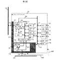
図1に本発明に係るデータ処理システムの一例を示す。本システムは第1の外部バス103に接続された第1のデータプロセッサ100と、第2の外部バス105に接続された第2のデータプロセッサ101で構成される。第1の外部バス103にはRAM、ROM,フラッシュメモリ(FLASH)等の複数の外部デバイス102が接続される。第2の外部バス105には、RAM、ROM、FLASH、液晶ディスプレイ(LCD)コントローラ等の外部デバイス104が接続されている。第2のデータプロセッサ101は、第1の外部バス103上のデバイスの1つとして第1の外部インタフェース回路119を介して第1の外部バス103に接続されている。
2. Details of Embodiment FIG. 1 shows an example of a data processing system according to the present invention. This system includes a
第2のデータプロセッサ101は、内部高速バス108と内部低速バス115を有する。前記内部高速バス108には、CPU109、キャッシュメモリ110、ディジタル信号処理プロセッサ(DSP)111、内部高速バス108と内部低速バス115との間のバスブリッジ回路としてのブリッジ回路112、第1の外部インタフェース回路119、第2の外部インタフェース回路113、及びRAM107が接続されている。前記内部低速バス115にはシリアルインタフェース回路(SCI)、USB(ユニバーサル・シリアル・バス)、タイマ、メモリカードインタフェース回路(MCIF)、IOポートのような汎用入出力ポート(IOP)、クロックパルスジェネレータ(CPG)、フラッシュメモリ等の周辺回路116が接続されている。図1においてクロックパルスジェネレータ(CPG)には参照符号116aが付され、汎用入出力ポート(IOP)には参照符号116bが付されている。
The
データ処理システムは、特に制限されないが、携帯電話システムとされる。このとき、第1のデータプロセッサ100はベースバンド処理を行なう。第2のデータプロセッサ101は液晶ディスプレイコントローラのような外部デバイス104に対して画像表示制御の為の制御と圧縮伸張などの信号処理を行なう。液晶ディスプレイコントローラを介する時刻表示などの制御は、特に制限されないが、第1のデータプロセッサ100が第2のデータプロセッサ101を経由して行なう。
The data processing system is not particularly limited, but is a mobile phone system. At this time, the
前記第1の外部インタフェース回路119は、前記第1のデータプロセッサ100が第2のデータプロセッサ101の内部バス例えば内部高速バス108のバス権を獲得することを可能にするものであり、内部バス108のバス権を獲得した第1のデータプロセッサ100による前記内部バス108に接続された入出力回路のアクセスを可能にする。入出力回路とは、DSP111のレジスタ等を意味する。要するに、第1のデータプロセッサ100は内部高速バス108のバスマスタとして動作することが可能にされる。そのようなバスマスタとしての動作制御は内部バス制御部106が行なう。
The first
また、前記第1の外部インタフェース回路119は前記RAMをCPU109と第1のデータプロセッサ100との共有メモリもしくは共有バッファとして動作制御する。即ち、CPU109からのRAM107へのアクセス要求と第1のデータプロセッサ100からRAM107へのアクセス要求とに排他的に応答してRAM107を動作させる。このRAM107に対する共有バッファ機能により、第1のデータプロセッサ100と第2のデータプロセッサ101との間のデータ転送を実現できる。このデータ転送には、例えば割込み信号117を用いたハンドシェーク制御を採用してよい。具体的には、第1のデータプロセッサ100からRAM107にデータが格納されると、CPU109の割込み信号117が与えられ、この割込みに応ずる割り込み処理にてCPU109がRAM107のデータを取りこむ。逆の場合には外部インタフェース回路119は第1のデータプロセッサ100に向けて割込み要求を発行する。
The first
前記第2の外部インタフェース回路113は外部バス105に接続される外部デバイスとのインタフェースを実現する為のインタフェース仕様を有する。例えば、外部デバイス104としてFLASH、液晶ディスプレイ(LCD)コントローラが接続することを想定している場合、第2の外部インタフェース回路113は、フラッシュメモリインタフェース回路、LCDインタフェース回路としてのインタフェース機能を有する。
The second
図1の構成において、前記領域118には、第2のデータプロセッサ101の待機状態において、前記第2の外部インタフェース回路113における外部バス105との接続端の代わりに、前記第1の外部インタフェース回路における外部バス103との接続端を、前記外部バス105に接続する切換え回路114が設けられている。即ち、前記切換え回路114は、第2のデータプロセッサ101の待機時に、第2の外部インタフェース回路113に代えて第1の外部バス103を第2の外部バス105へ接続する接続態様を選択する。これにより、第1のデータプロセッサ100は切換制御部114を介して、第2の外部バス105上のデバイスをアクセスすることが可能になる。例えば、第1のデータプロセッサ100は切換え回路114を介して外部バス105上の外部デバイス104として液晶ディスプレイコントローラを制御可能である。ここで図1の中の領域118の回路は第2のデータプロセッサ101の待機時にも動作する領域である。
In the configuration of FIG. 1, in the standby state of the
前記第2のデータプロセッサ101の待機状態は、当該第2のデータプロセッサ101に含まれるCPU109、DSP111、シリアルインタフェース回路、タイマ等のクロック同期回路へのクロック信号の供給が停止される状態である。例えば、CPU109がクロックパルスジェネレータ116aの待機状態レジスタに待機状態イネーブルビットをセットすることにより、クロックパルスジェネレータ116aはクロック信号CLKの出力動作もしくは発振動作を停止して、クロック信号の供給を抑止する。
The standby state of the
図1において120で示される回路は電源回路である。前記第2のデータプロセッサ101において前記切換え回路114の動作電源vdd1とその他の回路の動作電源vdd2とは分離可能とされる。例えば、動作電源vdd1の外部電源端子及び電源配線と、動作電源vdd2の外部電源端子及び電源配線とは、物理的に分離される。電源回路120は動作電源vdd1、vdd2を対応する電源端子に供給する。前記汎用入出力ポート116bは電源回路120に対する電源制御回路として利用される。汎用入出力ポート116bは前記第2のデータプロセッサ101の待機状態への遷移過程において前記その他の回路の全部又は一部への動作電源vdd2の供給を停止させる。前記切換え回路114には第2のデータプロセッサ101が動作可能なときは動作電源vdd1が常時供給される。待機状態から抜けるのに割込みを利用する場合には割込み制御回路には動作電源が供給されている。電源制御回路116bは、待機状態への遷移過程において電源回路120の電源制御レジスタを電源供給停止指示状態にセットする。これにより、動作電源vdd2の供給が停止される。電源制御レジスタに対する電源供給指示状態へのリセット動作は、待機状態から動作状態への復帰処理過程で行われればよい。
In FIG. 1, a circuit indicated by 120 is a power supply circuit. In the
図2に図1の第2のデータプロセッサ101の領域118の詳細図が例示される。更にこの例では、第1の外部インタフェース回路119が内部低速バス115のバスマスタとして信号線200で接続されている。図2の信号線200が示す通り、第1の外部インタフェース回路119がバスマスタとなる内部バスは高速バス108に限定されず、低速バスであてもよい。
FIG. 2 illustrates a detailed view of the
データプロセッサ1において領域118に構成される回路を第2の回路、その他の領域に構成されるCPU109などの回路を第1の回路と称する。領域118には、第1外部端子210、第1の外部端子と第1の回路を接続する第1バス211、第1の回路と第2の回路を接続する第2バス212、第1外部端子と第2の内部回路を接続する第3バス213、第2外部端子215、第2外部端子と第2の回路を接続する第4バス216、前記第2バス212と第3バス213の何れを第4バスに接続するかを選択するセレクタ217、バスドライバ218、及び第5バス219を有する。セレクタ217は待機状態への遷移過程で第1バス211を第4バス216に接続する接続形態を選択する。CPU109の状態に着目すると、待機状態は第1の回路による命令実行が抑止される状態(第1の状態)であり、動作状態は第1の回路が命令を実行可能な状態(第2の状態)である。第2のデータプロセッサ101は、待機状態において、第1の外部バス103を第2の外部バス105に直接接続することが可能となる。この例では、第2のデータプロセッサ101の待機状態において第1の外部バス103のデータを第2の外部バス105に無条件に伝達するように構成されているが、第1の外部バス103と第2の外部バス105を入出力バッファ(図示せず)を介して接続することも可能である。こうすれば第1の外部バス103から第2の外部バス105の入出力を制御することが可能となる。
In the data processor 1, a circuit configured in the
図1及び図2において第2のデータプロセッサ101は1個の半導体基板上に構成された、所謂シングルチップのデータプロセッサとして構成される。
1 and 2, the
図3にはマルチチップモジュールで第2のデータプロセッサ300を構成した場合の例が示される。第2のデータプロセッサ300は第1の外部インタフェース回路119及び切換え回路114の機能を内蔵したチップ301とそれ以外の機能を内蔵したチップ302で構成される。チップ302は内部高速バス108への接続部303を第1の外部インタフェース回路119とのインタフェース部としており、この接続部303に接続するチップ301が内部高速バス108のバスマスタになることが可能となる。第2のデータプロセッサ300の待機状態においてチップ301だけを動作させることにより、第1の外部バス103を第2の外部バス105へ接続することが可能になる。
FIG. 3 shows an example in which the
図4には第2のデータプロセッサ101が備える第1の外部インタフェース119の具体的な一例を示す。第1の外部インタフェース回路119は外部バスアクセス制御部401、バス変換調停部402、内部バスアクセス制御部403、RAMアクセス制御部404、リセット/割り込み制御部405から構成される。
FIG. 4 shows a specific example of the first
第1の外部バス103からのアクセス情報は外部バスアクセス制御部401に入力され、入力情報が同期化されてバス変換調停部402へ転送される。バス変換調停部は当該アクセスがRAM107へのアクセスか内部バス108へのアクセスかを判定し、内部バス108へのアクセスであった場合には内部バスアクセス制御部403へアクセス要求を出して内部バス108のバスアクセス仕様にしたがったバスアクセス動作を起動する。要するに、アドレス信号、バスアクセス制御信号、データを内部バス108のバスアクセス仕様に準拠してバス108に供給し、また、データをバス108から受取る。RAM107へのアクセス要求である場合にはRAMアクセス制御部404にメモリアクセス要求を出してRAM107のアクセス仕様に準拠してアクセス動作を起動する。要するに、アドレス信号、メモリ制御信号、データをメモリアクセス仕様にしたがってRAM107に供給し、また、データをRAM107から受取る。
Access information from the first
CPU109への割り込み/リセットの発行や、CPU109からの割り込みはリセット/割り込み制御部405で処理され、外部バスアクセス制御部401が第1の外部バス103上のデバイスに対して対応する要求を発行する。また、第1の外部バス103上のデバイスからの要求やRAMアクセス制御部404からの動作要求は外部バスアクセス制御部401が対応する割込み要求としてリセット/割り込み制御部405に与える。
Issuance of interrupts / resets to the
図5には第2のデータプロセッサ101が備える第1の外部インタフェース119の更に具体的な別の例を示す。同図には、バス103との間のインタフェース、バス115との間のインタフェース、RAM107との間のインタフェースとを実現する為の具体例を示す。第1の外部インタフェース回路119は、制御回路410、インデックスレジスタIDX、アドレスフラグFGを有する。制御回路410はアドレスレジスタADR、データレジスタDAT、コマンドレジスタCMD、アクセス制御レジスタACS、ステータスレジスタSTSなどの制御回路内蔵レジスタを有する。アドレスフラグFGは、論理値“1”が設定されると、インデックスレジスタIDXの選択を指定し、論理値“0”が設定されると制御回路内蔵レジスタの選択を指定する。論理値“0”が設定されたとき、制御回路内蔵レジスタの内のどのレジスタを選択するかはインデックスレジスタIDXの値で決まる。インデックスレジスタIDX及びアドレスフラグFGは第1の外部バス103を介してアクセスされる。バス103はデータバス103D、アドレスバス103A及びコントロールバス103Cから成る。インデックスレジスタIDXの値にしたがって制御回路内蔵レジスタが選択されて、対応するレジスタにデータバス103D経由でアドレス情報、データ情報、バスアクセス制御情報、コマンド情報がロードされ、ロードされたコマンド情報に従って、RAM107に対するアクセス、バス115に対するアクセスが起動される。この時のアクセスには前記レジスタの設定値が用いられ、アクセスタイミングはアクセス制御情報が決定する。外部バス103を介してRAM107に書き込まれたデータはCPU109が内部バス108を経由してアクセスすることができる。バス108はデータバス108D、アドレスバス108A及びコントロールバス108Cから成る。バス115はデータバス115D、アドレスバス115A及びコントロールバス115Cから成る。
FIG. 5 shows another more specific example of the first
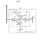
図6には本発明に係るデータ処理システムにおけるデータプロセッサのブートプログラムの初期的書き込みに関する例を示す。図6の例では、CPU109の内部バス115にメモリ502が配置され、また、第2の外部バス105にメモリ501が配置される。この例では、特に制限されないが、前記メモリ501,502はユーザプログラム格納領域として利用されることになる。その場合には、第2のデータプロセッサ101がリセット直後に実行するブートプログラムは、前記メモリ501又は502に通常格納される。図6では内部メモリ502を内部低速バス115に接続しているが、内部高速バス108に接続してもよい。第2のデータプロセッサの内部メモリ502はフラッシュメモリ等のような電気的に書き換え可能な不揮発性メモリであり、CPU109等と同じ半導体基板上に形成してもよく、或は異なる半導体基板上にそれぞれを形成し、1のパッケージに封入するものであってもよい。異なる半導体基板上に形成して1のパッケージに封入する場合、第2のデータプロセッサ101の内部バス108,115に接続するのではなく、パッケージ内部において第2の外部バス105に接続するようにしてもよい。ここでは、電気的に書き換え可能な不揮発性メモリ501,502をプログラムメモリとして利用する。
FIG. 6 shows an example relating to the initial writing of the boot program of the data processor in the data processing system according to the present invention. In the example of FIG. 6, the
前記電気的に書き込み可能な不揮発性メモリ501,502に対するプログラムの初期的な書き込みはデータプロセッサ101などの半導体集積回路の製造過程においてEPROMライタのような書込み装置を用いて行なうことが従来から行われてきた。図6の例では、データプロセッサ101がデータ処理システム上に実装された初期的な段階では不揮発性メモリ501,502にブートプログラムが初期書き込みされていない状態を想定する。図6のデータ処理システムはそのような状態からブートプログラムを初期的に書きこみ可能とするものである。要するに、第2のデータプロセッサ101のブートをRAM107から行える仕組みを第2のデータプロセッサ101に内蔵させる。即ち、第1のデータプロセッサ100から第1の外部バス103を経由して第2のデータプロセッサ101のブートプログラムをRAM107に書き込み、書き込み後に第2のデータプロセッサ101にRAM107のプログラムを実行させる。そのためには、第2のデータプロセッサ101をRAM107のプログラム実行により起動するかメモリ501又は502のプログラム実行により起動するかを切り替える必要がある。この切り換えは、リセット信号(RES)504によるリセット動作の指示に際してブートモード信号(BT)503のレベルを用いて行なう。例えばリセット信号504がローレベルの期間に、ブートモード信号503がハイレベルの時はRAM107のプログラム実行から起動し、ブートモード信号503がローレベルの時はメモリ501、502のプログラム実行から起動する。
Conventionally, initial writing of programs to the electrically writable
ブートプログラムの初期的書き込みの為の構成を詳述する。前記第2のデータプロセッサ101において、前記RAM107は、リセット信号504によるリセット動作解除後の第1動作モードにおいて前記第1のデータプロセッサ100により書き込み可能にされる。前記第1動作モードは、例えばリセット信号504がローレベルされるリセット期間に、ブートモード信号503がハイレベルにされていて、リセット信号504がハイレベルにネゲートされてリセット動作が解除された動作状態である。このとき、CPU109は命令フェッチが抑制される。要するに、CPU109に対するスタートベクタの供給が抑制されている。このときのRAM107に対するアクセスは前述の通り、第1のデータプロセッサ100が第1の外部インタフェース回路106に対して行なえばよい。データプロセッサ100によるRAM107への書き込みが終了すると、データプロセッサ100から第1の外部インタフェース回路119に与えられるコマンドにより、或はブートモード信号503のハイレベルからローレベルへの変化に応答して、CPU109にRAM107の先頭アドレスを指定するスタートベクタが供給される。これによってCPU109はRAM107に格納されたプログラムを実行する。ここでは、ユーザプログラムの初期的な書き込みという操作に着目しているのであるから、RAM107に格納される前記プログラムは少なくともユーザプログラムの書き込み制御プログラムであればよい。ユーザプログラム自体も前記プログラムと一緒にRAM107に予め転送されていてよい。或は、RAM107に転送された書き込み制御プログラムの実行により、ユーザプログラムをシリアルインタフェース回路116等から取り込んでメモリ502などに初期的に書き込むようにしてもよい。
A configuration for initial writing of the boot program will be described in detail. In the
リセット動作解除後の第2動作モードではCPU109による命令フェッチの対象は、前記メモリ501又は502である。前記第2動作モードは、例えばリセット信号504がローレベルにされるリセット期間に、ブートモード信号503がローレベルにされて、リセット信号504がハイレベルにネゲートされてリセット動作が解除された動作状態である。これにより、CPU109は前記第1動作モードを介して前記メモリ501又は502に初期的に格納されたユーザプログラムを実行する。
In the second operation mode after the reset operation is released, the target of instruction fetching by the
前記第1のデータプロセッサ100からRAM107へブートプログラムとしての前記書き込み制御用プログラムを格納する動作を説明する。
An operation of storing the write control program as a boot program from the
先ず、第2のデータプロセッサ101をブートする前に、第1のデータプロセッサ100に接続しているメモリ505もしくはメモリカード506などの外部記憶もしくは図示を省略するシリアルインタフェースなどから入力したブートプログラムを第1のデータプロセッサ100が第2のデータプロセッサ101のRAM107に書き込む。
First, before the
RAM107に転送するブートプログラムはアプリケーションまでを含んだものでも構わないが、次のような処理を含んでいれば短いブートプログラムで対応可能となる。例えば、RAM107上のプログラムには、第1のデータプロセッサ100から第1の外部インターフェイス回路119を介してプログラムの転送を行なってメモリ501又は502に書き込むプログラムが格納されている。或は、第2のデータプロセッサの周辺デバイス116のシリアル、USB、メモリカードを用いて、プログラムをメモリ501、502に転送して書き込むプログラムが格納される。
The boot program transferred to the
上記より、第2のデータプロセッサ101のブート用メモリ501、502がフラッシュメモリであった場合に、システム組み立ての後工程において本来ならフラッシュメモリを初期化する仕組みが必要であったが、RAM107からブートするモードでフラッシュメモリの初期化を行うことができるようになるため、データプロセッサ101の量産コストを低減することが可能になる。
From the above, when the
図7には図6のデータ処理システムにおけるブート動作のタイミングチャートが例示される。 FIG. 7 illustrates a timing chart of the boot operation in the data processing system of FIG.
第1のデータプロセッサ100はブートモード信号503とリセット信号504を供給し、第2のデータプロセッサ101の起動を制御する。
The
第1のデータプロセッサはブートモード信号503をハイレベルにしてリセットを解除(リセット信号をローレベルからハイレベルに遷移)することで、RAM107からブートするモードで第2のデータプロセッサを起動し、第1の外部バス103を介してRAM107にブートプログラムを転送する。第2のデータプロセッサのCPU109は、ブートモード信号がハイレベルであることを検出し、第1の外部インターフェイス回路119を介してRAM107からブートプログラムをフェッチする。CPU109は、ブートプログラムの転送中には命令フェッチが抑止されるため、ブートプログラムの供給が行われず、ウェイトした状態におかれる。ブートプログラムの転送終了にあわせて第1のデータプロセッサ100は転送終了コマンドを第1の外部インターフェイス回路119に転送し、第1の外部インターフェイス回路119はCPU109にブートプログラムのフェッチを指示することで、第2のデータプロセッサ101はRAM107のプログラムで起動する。CPU109はRAM107内のブートプログラムを実行し、内部高速バス108を経由して、メモリ501,502にブートプログラムを書き込む処理を行なう。メモリ501,502へのブートプログラムの書込みが終了した段階で再度第2のデータプロセッサ101をリセットし(リセット信号(RES)504をハイレベルからローレベルに遷移)、次はブートモード信号(BT)503をローレベルにした状態でリセットを解除し、第2のデータプロセッサ101を起動する。これによりCPU109は、メモリ501,502からブートプログラムをフェッチし、これを実行することにより、第2のデータプロセッサのデータ処理動作が起動される。
The first data processor sets the
図7の例は、第1の外部バス103を介して、第1のデータプロセッサ100に接続しているメモリ505若しくはメモリカード506からメモリ501,502にブートプログラムを供給する動作タイミングを示している。
The example of FIG. 7 shows the operation timing of supplying the boot program from the
図8には図6のデータ処理システムにおけるブート動作の別のタイミングチャートが例示される。同図に示されるタイミングは、第2のデータプロセッサ101にあるシリアルやUSB116等を介してメモリ501,502に格納するブートプログラムを供給する場合を想定している。その他の点は図7と同じである。
FIG. 8 illustrates another timing chart of the boot operation in the data processing system of FIG. The timing shown in the figure assumes a case in which a boot program stored in the
図9にはメモリ501又は502にブートプログラムが格納されている状態において、ブートプログラムの更新又は第2のデータプロセッサ101で実行されるアプリケーションを追加/更新する場合のタイミングチャートが例示される。
FIG. 9 illustrates a timing chart when the boot program is updated or an application executed by the
第1のデータプロセッサ100はブートモード信号503をローレベルにしてリセットを解除することで、第2のデータプロセッサ101はメモリ501,502からブートプログラムをフェッチし起動を開始する。メモリ501,502には予めブートプログラムの更新又はプロセッサ2で実行されるアプリケーションを追加/更新するための転送プログラムが格納されており、第1のデータプロセッサ100からの起動指示等により転送プログラムが起動される。例えば第1のデータプロセッサ100に接続されるアンテナを介して、無線通信により追加のアプリケーションを受信する場合、第1のプロセッサ100は受信した追加のアプリケーションを外部バス103を介してRAM107に転送する。第2のデータプロセッサ101はRAM107に格納された追加のアプリケーションを第1の外部インターフェイス回路119を介して内部バス108に取り込み、メモリ501又は502に転送して書込を行う。
The
図10には図3のデータプロセッサ300を構成するマルチチップモジュールの断面図が例示される。高密度実装基板510の一面には、ガラスエポキシ基板で成るようなプリント配線基板の実装面に接続されるバンプ電極511が多数配列され、他方の面には前記バンプ電極511に接続されたマイクロバンプ電極512及びパッド電極513が多数配置される。マイクロバンプ電極512の一部には前記半導体チップ302のボンディングパッドがフェースダウンで実装される。前記半導体チップ302の上に別の半導体チップ301が積層配置され、この半導体チップ301のボンディングパッドはボンディングワイヤ515にて対応する前記パッド電極513に接続される。ボンディングワイヤ515及び半導体チップ301,302の全体は樹脂516でモールドされる。
FIG. 10 illustrates a cross-sectional view of a multi-chip module constituting the
以上本発明者によってなされた発明を具体的に説明したが、本発明はそれに限定されるものではなく、その要旨を逸脱しない範囲において種々変更可能であることは言うまでもない。 Although the invention made by the inventor has been specifically described above, the present invention is not limited thereto, and it goes without saying that various changes can be made without departing from the scope of the invention.
例えばデータプロセッサが内蔵する周辺回路やその他の回路モジュールは図1などに基づいて説明した回路に限定されず適宜変更することが可能である。データプロセッサの内部バスは高速バスと低速バスに別れていなくてもよい。また、第1の回路部と第2の回路部に対する動作電源系統は外部電源端子から別々にしなくても、スイッチ回路で電源供給の停止を制御できるようにしてもよい。また、データプロセッサをマルチチップモジュールとして構成するとき、登載する半導体集積回路の種類は上記の例に限定されず、フラッシュッメモリ502のような半導体チップと、その他CPU109などのプロセッサコアチップ、及び半導体チップ301のようなインタフェースチップを合計3枚登載してもよい。フラッシュメモリチップはマルチチップモジュールに複数チップ登載してもよい。
For example, the peripheral circuits and other circuit modules built in the data processor are not limited to the circuits described with reference to FIG. 1 and can be changed as appropriate. The internal bus of the data processor may not be divided into a high speed bus and a low speed bus. Further, the operation power supply system for the first circuit portion and the second circuit portion may not be separately provided from the external power supply terminal, and the stop of power supply may be controlled by the switch circuit. Further, when the data processor is configured as a multichip module, the type of semiconductor integrated circuit to be mounted is not limited to the above example, and a semiconductor chip such as
本発明は、携帯電話システム、更には表示制御システム、プリンタシステム、その他の携帯情報端末等、複数のデータプロセッサを用いて処理負担の分散を企図したデータ処理システム、そしてそのようなデータ処理システムに利用するデータプロセッサに広く適用することができる。 The present invention relates to a data processing system that intends to distribute processing load using a plurality of data processors, such as a mobile phone system, a display control system, a printer system, and other portable information terminals, and to such a data processing system. The present invention can be widely applied to data processors to be used.
100 第1のデータプロセッサ
101 第2のデータプロセッサ
103 第1のバス
105 第2のバス
113 第2の外部インタフェース回路
114 切換え回路
119 第1の外部インタフェース回路
DESCRIPTION OF
Claims (1)
前記第2のデータプロセッサは、前記第1のデータプロセッサが前記第2のデータプロセッサの内部バスのバス権を獲得することを可能とするインタフェース手段を内蔵し、
前記インタフェース手段は、前記内部バスのバス権を獲得した第1のデータプロセッサによる前記内部バスに接続された入出力回路のアクセスを可能にするものである、ことを特徴とするデータ処理システム。 A data processing system including a first data processor and a second data processor,
The second data processor includes interface means that allows the first data processor to acquire the bus right of the internal bus of the second data processor;
The data processing system according to claim 1, wherein the interface means enables an input / output circuit connected to the internal bus to be accessed by a first data processor that has acquired the bus right of the internal bus.
Priority Applications (1)
| Application Number | Priority Date | Filing Date | Title |
|---|---|---|---|
| JP2009193040A JP4822465B2 (en) | 2001-01-31 | 2009-08-24 | Data processing system |
Applications Claiming Priority (3)
| Application Number | Priority Date | Filing Date | Title |
|---|---|---|---|
| JP2001022587 | 2001-01-31 | ||
| JP2001022587 | 2001-01-31 | ||
| JP2009193040A JP4822465B2 (en) | 2001-01-31 | 2009-08-24 | Data processing system |
Related Parent Applications (1)
| Application Number | Title | Priority Date | Filing Date |
|---|---|---|---|
| JP2008130499A Division JP2008269627A (en) | 2001-01-31 | 2008-05-19 | Data processing system |
Related Child Applications (2)
| Application Number | Title | Priority Date | Filing Date |
|---|---|---|---|
| JP2010000592A Division JP2010146579A (en) | 2001-01-31 | 2010-01-05 | Single chip data processor and semiconductor integrated circuit |
| JP2011011770A Division JP4822472B2 (en) | 2001-01-31 | 2011-01-24 | Data processing system |
Publications (3)
| Publication Number | Publication Date |
|---|---|
| JP2010009612A true JP2010009612A (en) | 2010-01-14 |
| JP2010009612A5 JP2010009612A5 (en) | 2010-02-25 |
| JP4822465B2 JP4822465B2 (en) | 2011-11-24 |
Family
ID=18887981
Family Applications (8)
| Application Number | Title | Priority Date | Filing Date |
|---|---|---|---|
| JP2002561694A Pending JPWO2002061591A1 (en) | 2001-01-31 | 2001-10-24 | Data processing system and data processor |
| JP2004345686A Expired - Lifetime JP3896372B2 (en) | 2001-01-31 | 2004-11-30 | Data processing system |
| JP2004345687A Withdrawn JP2005115964A (en) | 2001-01-31 | 2004-11-30 | Data processing system |
| JP2008130499A Pending JP2008269627A (en) | 2001-01-31 | 2008-05-19 | Data processing system |
| JP2008130498A Pending JP2008269626A (en) | 2001-01-31 | 2008-05-19 | Data processing system |
| JP2009193040A Expired - Lifetime JP4822465B2 (en) | 2001-01-31 | 2009-08-24 | Data processing system |
| JP2010000592A Withdrawn JP2010146579A (en) | 2001-01-31 | 2010-01-05 | Single chip data processor and semiconductor integrated circuit |
| JP2011011770A Expired - Lifetime JP4822472B2 (en) | 2001-01-31 | 2011-01-24 | Data processing system |
Family Applications Before (5)
| Application Number | Title | Priority Date | Filing Date |
|---|---|---|---|
| JP2002561694A Pending JPWO2002061591A1 (en) | 2001-01-31 | 2001-10-24 | Data processing system and data processor |
| JP2004345686A Expired - Lifetime JP3896372B2 (en) | 2001-01-31 | 2004-11-30 | Data processing system |
| JP2004345687A Withdrawn JP2005115964A (en) | 2001-01-31 | 2004-11-30 | Data processing system |
| JP2008130499A Pending JP2008269627A (en) | 2001-01-31 | 2008-05-19 | Data processing system |
| JP2008130498A Pending JP2008269626A (en) | 2001-01-31 | 2008-05-19 | Data processing system |
Family Applications After (2)
| Application Number | Title | Priority Date | Filing Date |
|---|---|---|---|
| JP2010000592A Withdrawn JP2010146579A (en) | 2001-01-31 | 2010-01-05 | Single chip data processor and semiconductor integrated circuit |
| JP2011011770A Expired - Lifetime JP4822472B2 (en) | 2001-01-31 | 2011-01-24 | Data processing system |
Country Status (8)
| Country | Link |
|---|---|
| US (9) | US7401163B2 (en) |
| EP (2) | EP1679590B1 (en) |
| JP (8) | JPWO2002061591A1 (en) |
| KR (5) | KR100995719B1 (en) |
| CN (4) | CN1932788B (en) |
| DE (2) | DE60144303D1 (en) |
| TW (1) | TW594484B (en) |
| WO (1) | WO2002061591A1 (en) |
Cited By (1)
| Publication number | Priority date | Publication date | Assignee | Title |
|---|---|---|---|---|
| US8291124B2 (en) | 2010-02-24 | 2012-10-16 | Renesas Electronics Corporation | Semiconductor device and data processing system having a reduced number of terminals allocated for externally accessed address |
Families Citing this family (59)
| Publication number | Priority date | Publication date | Assignee | Title |
|---|---|---|---|---|
| US20020045477A1 (en) | 1999-08-03 | 2002-04-18 | Dabrowski Stanley P. | Method and apparatus for scrip distribution and management permitting redistribution of issued scrip |
| DE60144303D1 (en) | 2001-01-31 | 2011-05-05 | Renesas Electronics Corp | Data processing system |
| US7450963B2 (en) * | 2002-08-27 | 2008-11-11 | Qualcomm Incorporated | Low power dual processor architecture for multi mode devices |
| JP2004297632A (en) * | 2003-03-28 | 2004-10-21 | Renesas Technology Corp | Microprocessor and mobile communication terminal |
| JP2005011166A (en) * | 2003-06-20 | 2005-01-13 | Renesas Technology Corp | Information processor |
| US20110151609A1 (en) * | 2004-07-26 | 2011-06-23 | Kuo-Ching Chiang | Method for Forming Thin Film Heat Dissipater |
| US20060026417A1 (en) * | 2004-07-30 | 2006-02-02 | Information Assurance Systems L.L.C. | High-assurance secure boot content protection |
| DE102004041805A1 (en) * | 2004-08-24 | 2006-03-09 | Siemens Ag | Baseband chip, communication module, printed circuit board with peripheral devices and methods for controlling such peripheral devices |
| JP2006099704A (en) * | 2004-09-30 | 2006-04-13 | Toshiba Corp | Information processor and startup control method |
| US7353317B2 (en) | 2004-12-28 | 2008-04-01 | Intel Corporation | Method and apparatus for implementing heterogeneous interconnects |
| US7548749B2 (en) * | 2005-02-28 | 2009-06-16 | Microsoft Corporation | High-speed internal wireless bus |
| JP4569368B2 (en) * | 2005-04-26 | 2010-10-27 | 日本電気株式会社 | Computer system, memory initialization method, and computer system program |
| US7890736B2 (en) * | 2005-11-08 | 2011-02-15 | St-Ericsson Sa | Control device with flag registers for synchronization of communications between cores |
| KR101275752B1 (en) | 2005-12-06 | 2013-06-17 | 삼성전자주식회사 | Memory system and booting method thereof |
| JP2007157150A (en) * | 2005-12-06 | 2007-06-21 | Samsung Electronics Co Ltd | Memory system and memory processing method including the same |
| US7717350B2 (en) * | 2006-06-30 | 2010-05-18 | Advanced Micro Devices, Inc. | Portable computing platform having multiple operating modes and heterogeneous processors |
| EP3731086A1 (en) | 2006-08-31 | 2020-10-28 | SnapTrack, Inc. | Multi-core device with optimized memory configuration |
| US7709861B2 (en) * | 2006-09-11 | 2010-05-04 | Agere Systems Inc. | Systems and methods for supporting a subset of multiple interface types in a semiconductor device |
| US7882379B2 (en) * | 2006-09-22 | 2011-02-01 | Sony Computer Entertainment Inc. | Power consumption reduction in a multiprocessor system |
| JP4976817B2 (en) * | 2006-11-06 | 2012-07-18 | オンセミコンダクター・トレーディング・リミテッド | Program processing apparatus and program processing method |
| US20080155296A1 (en) * | 2006-12-22 | 2008-06-26 | Fujitsu Limited | Apparatus for controlling clock signals to processor circuit |
| WO2008086419A2 (en) * | 2007-01-09 | 2008-07-17 | Sr Télécom & Co, S.E.C. | Base station with redundant baseband processing units |
| JP4785142B2 (en) * | 2007-01-31 | 2011-10-05 | ルネサスエレクトロニクス株式会社 | Data processing device |
| US7827515B2 (en) * | 2007-03-15 | 2010-11-02 | Oracle America, Inc. | Package designs for fully functional and partially functional chips |
| WO2009011104A1 (en) * | 2007-07-18 | 2009-01-22 | Panasonic Corporation | Video audio processing apparatus and standby and reset method thereof |
| JP5111191B2 (en) | 2008-03-27 | 2012-12-26 | ルネサスエレクトロニクス株式会社 | Data processing apparatus, image encoding / decoding apparatus, data processing system, and image processing apparatus |
| JP2010003151A (en) * | 2008-06-20 | 2010-01-07 | Renesas Technology Corp | Data processing apparatus |
| US7827336B2 (en) * | 2008-11-10 | 2010-11-02 | Freescale Semiconductor, Inc. | Technique for interconnecting integrated circuits |
| JPWO2010073444A1 (en) * | 2008-12-24 | 2012-05-31 | パナソニック株式会社 | Bus controller and initial boot program patch method |
| EP2228730A1 (en) * | 2009-03-10 | 2010-09-15 | ST-Ericsson SA | Electronic device having external data transfer functionality |
| KR20100121215A (en) * | 2009-05-08 | 2010-11-17 | 삼성전자주식회사 | Semiconductor device and method for writing os image using the same |
| CN101697198B (en) * | 2009-10-28 | 2011-07-27 | 浪潮电子信息产业股份有限公司 | Method for dynamically regulating number of active processors in single computer system |
| US8838949B2 (en) * | 2010-03-22 | 2014-09-16 | Qualcomm Incorporated | Direct scatter loading of executable software image from a primary processor to one or more secondary processor in a multi-processor system |
| US9058191B2 (en) * | 2010-03-22 | 2015-06-16 | Qualcomm Incorporated | Direct transfer of executable software image to memory allocated by target processor based on transferred image header |
| DE102010034991A1 (en) * | 2010-08-20 | 2012-02-23 | Abb Ag | Installation device with universal data coupling in building system technology and arrangements with such trained installation equipment |
| KR101691091B1 (en) | 2010-11-08 | 2016-12-30 | 삼성전자주식회사 | Computing system and hibernation method thereof |
| EP2671228B1 (en) | 2011-02-01 | 2022-04-13 | 3M Innovative Properties Company | A passive interface for an electronic memory device |
| WO2013062975A1 (en) * | 2011-10-24 | 2013-05-02 | Skyworks Solutions, Inc. | Dual mode power amplifier control interface |
| CN104410373B (en) | 2012-06-14 | 2016-03-09 | 西凯渥资讯处理科技公司 | Comprise the power amplifier module of related system, device and method |
| JP5949330B2 (en) * | 2012-08-29 | 2016-07-06 | 株式会社リコー | Information processing apparatus and information processing method |
| CN103399828B (en) * | 2013-07-23 | 2015-12-23 | 杭州华三通信技术有限公司 | Based on startup switching control and the method for active and standby storer |
| CN104462010B (en) * | 2013-09-13 | 2018-08-31 | 联想(北京)有限公司 | A kind of electronic equipment and condition control method |
| JP2017503458A (en) * | 2013-10-25 | 2017-01-26 | エルジー・ケム・リミテッド | Battery management system that can transmit secondary protection signals and diagnostic signals using a small number of isolation elements |
| CN103885908B (en) * | 2014-03-04 | 2017-01-25 | 中国科学院计算技术研究所 | Data transmission system and method based on external device and accessible registers |
| JP6421452B2 (en) * | 2014-05-20 | 2018-11-14 | ブラザー工業株式会社 | Copier, computer program for copier, and method executed by copier |
| KR101598771B1 (en) * | 2014-06-11 | 2016-03-02 | 주식회사 슈프리마에이치큐 | Method and apparatus for authenticating biometric by using face recognizing |
| JP6570227B2 (en) * | 2014-08-28 | 2019-09-04 | キヤノン株式会社 | Information processing apparatus including main system and subsystem |
| JP6394291B2 (en) * | 2014-11-05 | 2018-09-26 | 株式会社デンソー | Electronic control device and memory rewriting method |
| CN105611409B (en) * | 2016-01-04 | 2019-12-27 | 京东方科技集团股份有限公司 | Advertising machine control system and control method thereof and advertising machine |
| US10664276B2 (en) | 2016-09-28 | 2020-05-26 | International Business Machines Corporation | Remote command invocation using a register for storing a command and an attention bit indicating command has been issued |
| DE102017212252A1 (en) * | 2017-07-18 | 2019-01-24 | Robert Bosch Gmbh | Method and device for initial programming of a slave computer |
| CN107832244B (en) * | 2017-10-18 | 2020-10-20 | 北京全路通信信号研究设计院集团有限公司 | Processor system of safety computer |
| US10839641B2 (en) | 2018-02-27 | 2020-11-17 | Stanley P. Dabrowski | Method and apparatus for modifying gaming machines to provide supplemental or modified functionality |
| WO2020054060A1 (en) * | 2018-09-14 | 2020-03-19 | 株式会社ソシオネクスト | Moving image encoding method and moving image encoding apparatus |
| US11112849B2 (en) * | 2018-10-26 | 2021-09-07 | Silicon Laboratories Inc. | Method and apparatus for selectable high performance or low power processor system |
| US11113072B2 (en) * | 2019-08-02 | 2021-09-07 | Arista Networks, Inc. | Boot personality for network device |
| US20220391346A1 (en) * | 2019-12-12 | 2022-12-08 | Sony Semiconductor Solutions Corporation | Communication apparatus and communication system |
| CN112035398B (en) * | 2020-08-25 | 2023-10-24 | 青岛信芯微电子科技股份有限公司 | System-on-chip (SoC) and data processing method suitable for SoC |
| CN112835826A (en) * | 2021-03-04 | 2021-05-25 | 深圳市广和通无线股份有限公司 | Communication method, device, equipment and readable storage medium |
Citations (4)
| Publication number | Priority date | Publication date | Assignee | Title |
|---|---|---|---|---|
| JPH05346864A (en) * | 1991-02-15 | 1993-12-27 | Fujitsu Ltd | Fault processing system for information processor |
| JPH08101609A (en) * | 1994-09-30 | 1996-04-16 | Ricoh Co Ltd | Image forming device |
| JPH09128323A (en) * | 1995-08-31 | 1997-05-16 | Seiko Epson Corp | Information processor and control method for information processor |
| JP2000132284A (en) * | 1998-10-27 | 2000-05-12 | Canon Inc | Electronic equipment, method for reducing its power consumption, recoding device, and method for reducing its power consumption |
Family Cites Families (46)
| Publication number | Priority date | Publication date | Assignee | Title |
|---|---|---|---|---|
| JPS57174701A (en) * | 1981-04-20 | 1982-10-27 | Hitachi Ltd | Decentralized controlling system |
| JPS5839341A (en) * | 1981-09-02 | 1983-03-08 | Toshiba Corp | Method and device for data access control of data base management system |
| JPH0644776B2 (en) | 1986-11-19 | 1994-06-08 | 富士通株式会社 | Line control device |
| JPS63148364A (en) | 1986-12-12 | 1988-06-21 | Oki Electric Ind Co Ltd | Shared memory access system |
| JP2664777B2 (en) * | 1989-08-02 | 1997-10-22 | 株式会社日立製作所 | Function expansion method |
| JPH04276838A (en) | 1991-03-04 | 1992-10-01 | Toshiba Corp | Cpu with built-in memory |
| JP3461825B2 (en) * | 1991-06-26 | 2003-10-27 | 三星電子株式会社 | Multiprocessor distributed initialization and self-test system |
| JPH0534684A (en) | 1991-07-30 | 1993-02-12 | Sharp Corp | Projection type picture displaying device |
| JPH05151075A (en) | 1991-11-28 | 1993-06-18 | Oki Electric Ind Co Ltd | Memory protection device |
| JP3058986B2 (en) | 1992-04-02 | 2000-07-04 | ダイヤセミコンシステムズ株式会社 | Computer system power saving controller |
| US5742760A (en) * | 1992-05-12 | 1998-04-21 | Compaq Computer Corporation | Network packet switch using shared memory for repeating and bridging packets at media rate |
| JPH06139063A (en) | 1992-10-23 | 1994-05-20 | Nec Corp | Firmware rewriting system |
| JP2556268B2 (en) * | 1993-07-20 | 1996-11-20 | 日本電気株式会社 | Program download method |
| US8509260B2 (en) * | 1993-08-31 | 2013-08-13 | Broadcom Corporation | Modular, portable data processing terminal for use in a communication network |
| JPH0837546A (en) | 1993-11-18 | 1996-02-06 | Dsp Telecommun Ltd | Base band processor for personal digital portable telephone(pdc) and demodulation of phase-modulated signal |
| IL107656A (en) * | 1993-11-18 | 1996-11-14 | Dsp Telecomm Ltd | Demodulator |
| US5481186A (en) | 1994-10-03 | 1996-01-02 | At&T Corp. | Method and apparatus for integrated testing of a system containing digital and radio frequency circuits |
| JP3799642B2 (en) | 1996-01-10 | 2006-07-19 | ソニー株式会社 | Software update system for communication terminal, communication terminal and communication management center |
| US5822553A (en) * | 1996-03-13 | 1998-10-13 | Diamond Multimedia Systems, Inc. | Multiple parallel digital data stream channel controller architecture |
| US6370546B1 (en) * | 1996-04-08 | 2002-04-09 | Sony Corporation | First information processing device directly accessing, updating second information process device and vice versa via transmission bus management authority |
| US5805882A (en) * | 1996-07-19 | 1998-09-08 | Compaq Computer Corporation | Computer system and method for replacing obsolete or corrupt boot code contained within reprogrammable memory with new boot code supplied from an external source through a data port |
| US5991817A (en) * | 1996-09-06 | 1999-11-23 | Cisco Systems, Inc. | Apparatus and method for a network router |
| TW382670B (en) * | 1996-11-21 | 2000-02-21 | Hitachi Ltd | Low power processor |
| US5768289A (en) * | 1997-05-22 | 1998-06-16 | Intel Corporation | Dynamically controlling the number of boundary-scan cells in a boundary-scan path |
| JP3070527B2 (en) * | 1997-06-10 | 2000-07-31 | 日本電気株式会社 | Wireless mobile terminal |
| US6067595A (en) * | 1997-09-23 | 2000-05-23 | Icore Technologies, Inc. | Method and apparatus for enabling high-performance intelligent I/O subsystems using multi-port memories |
| JP3826517B2 (en) | 1997-10-27 | 2006-09-27 | ソニー株式会社 | Image processing device |
| US6675233B1 (en) * | 1998-03-26 | 2004-01-06 | O2 Micro International Limited | Audio controller for portable electronic devices |
| US6163828A (en) * | 1998-05-22 | 2000-12-19 | Lucent Technologies Inc. | Methods and apparatus for providing multi-processor access to shared memory |
| US6260166B1 (en) * | 1998-06-01 | 2001-07-10 | Compaq Computer Corporation | Observability register architecture for efficient production test and debug |
| JP2000010702A (en) | 1998-06-23 | 2000-01-14 | Pioneer Electron Corp | Method and device for picture display menu selection |
| FI982194A0 (en) * | 1998-10-09 | 1998-10-09 | Nokia Mobile Phones Ltd | Procedure for installing one or more operating systems / user interfaces in an electronic device and electronic device |
| JP2000164796A (en) * | 1998-11-27 | 2000-06-16 | Nec Corp | Multichip module |
| JP3623379B2 (en) * | 1998-12-01 | 2005-02-23 | 富士通株式会社 | Microprocessor |
| JP3895071B2 (en) * | 1999-03-12 | 2007-03-22 | インターナショナル・ビジネス・マシーンズ・コーポレーション | Bus / bridge circuit, information processing system, and card bus controller |
| JP2000298585A (en) | 1999-04-13 | 2000-10-24 | Seiko Epson Corp | System and method for rewriting rom |
| US6738845B1 (en) * | 1999-11-05 | 2004-05-18 | Analog Devices, Inc. | Bus architecture and shared bus arbitration method for a communication device |
| US6501999B1 (en) * | 1999-12-22 | 2002-12-31 | Intel Corporation | Multi-processor mobile computer system having one processor integrated with a chipset |
| US6907264B1 (en) * | 2000-08-09 | 2005-06-14 | Lucent Technologies Inc. | Methods and apparatus for modularization of real time and task oriented features in wireless communications |
| JP2002091636A (en) * | 2000-09-20 | 2002-03-29 | Seiko Epson Corp | Information processor |
| US6802018B2 (en) * | 2000-12-27 | 2004-10-05 | Intel Corporation | Method and apparatus to directly access a peripheral device when central processor operations are suspended |
| US20020124125A1 (en) * | 2000-12-29 | 2002-09-05 | David Bormann | Method and apparatus to permit a peripheral device to become the default system bus master |
| DE60144303D1 (en) * | 2001-01-31 | 2011-05-05 | Renesas Electronics Corp | Data processing system |
| JP4974202B2 (en) * | 2001-09-19 | 2012-07-11 | ルネサスエレクトロニクス株式会社 | Semiconductor integrated circuit |
| US6925510B2 (en) * | 2002-02-22 | 2005-08-02 | Winbond Electronics, Corp. | Peripheral or memory device having a combined ISA bus and LPC bus |
| JP5151075B2 (en) | 2005-06-21 | 2013-02-27 | ソニー株式会社 | Image processing apparatus, image processing method, imaging apparatus, and computer program |
-
2001
- 2001-10-24 DE DE60144303T patent/DE60144303D1/en not_active Expired - Lifetime
- 2001-10-24 EP EP06004268A patent/EP1679590B1/en not_active Expired - Lifetime
- 2001-10-24 KR KR1020097009694A patent/KR100995719B1/en not_active IP Right Cessation
- 2001-10-24 JP JP2002561694A patent/JPWO2002061591A1/en active Pending
- 2001-10-24 CN CN2006100959803A patent/CN1932788B/en not_active Expired - Fee Related
- 2001-10-24 KR KR1020107010296A patent/KR100994003B1/en not_active IP Right Cessation
- 2001-10-24 KR KR1020087017164A patent/KR100946831B1/en active IP Right Grant
- 2001-10-24 WO PCT/JP2001/009322 patent/WO2002061591A1/en active IP Right Grant
- 2001-10-24 CN CNB018223982A patent/CN1251105C/en not_active Expired - Fee Related
- 2001-10-24 CN CN2006100997928A patent/CN1936876B/en not_active Expired - Fee Related
- 2001-10-24 KR KR1020037009715A patent/KR100923370B1/en not_active IP Right Cessation
- 2001-10-24 KR KR1020097010017A patent/KR101046876B1/en not_active IP Right Cessation
- 2001-10-24 CN CN2006100582258A patent/CN1818894B/en not_active Expired - Fee Related
- 2001-10-24 DE DE60132817T patent/DE60132817T2/en not_active Expired - Lifetime
- 2001-10-24 EP EP01978873A patent/EP1359510B1/en not_active Expired - Lifetime
- 2001-10-24 US US10/470,758 patent/US7401163B2/en not_active Expired - Lifetime
- 2001-12-27 TW TW090132574A patent/TW594484B/en not_active IP Right Cessation
-
2004
- 2004-11-30 JP JP2004345686A patent/JP3896372B2/en not_active Expired - Lifetime
- 2004-11-30 JP JP2004345687A patent/JP2005115964A/en not_active Withdrawn
-
2005
- 2005-08-15 US US11/203,210 patent/US7401165B2/en not_active Expired - Lifetime
-
2008
- 2008-05-19 JP JP2008130499A patent/JP2008269627A/en active Pending
- 2008-05-19 JP JP2008130498A patent/JP2008269626A/en active Pending
- 2008-06-04 US US12/155,412 patent/US7725616B2/en not_active Expired - Lifetime
-
2009
- 2009-05-22 US US12/470,988 patent/US7975077B2/en not_active Expired - Fee Related
- 2009-08-24 JP JP2009193040A patent/JP4822465B2/en not_active Expired - Lifetime
-
2010
- 2010-01-05 JP JP2010000592A patent/JP2010146579A/en not_active Withdrawn
-
2011
- 2011-01-24 JP JP2011011770A patent/JP4822472B2/en not_active Expired - Lifetime
- 2011-02-11 US US13/025,785 patent/US8244926B2/en not_active Expired - Lifetime
-
2012
- 2012-07-23 US US13/555,786 patent/US8595388B2/en not_active Expired - Lifetime
-
2013
- 2013-10-18 US US14/057,442 patent/US8812750B2/en not_active Expired - Fee Related
-
2014
- 2014-07-09 US US14/326,868 patent/US9069911B2/en not_active Expired - Fee Related
-
2015
- 2015-05-22 US US14/720,028 patent/US20150253832A1/en not_active Abandoned
Patent Citations (4)
| Publication number | Priority date | Publication date | Assignee | Title |
|---|---|---|---|---|
| JPH05346864A (en) * | 1991-02-15 | 1993-12-27 | Fujitsu Ltd | Fault processing system for information processor |
| JPH08101609A (en) * | 1994-09-30 | 1996-04-16 | Ricoh Co Ltd | Image forming device |
| JPH09128323A (en) * | 1995-08-31 | 1997-05-16 | Seiko Epson Corp | Information processor and control method for information processor |
| JP2000132284A (en) * | 1998-10-27 | 2000-05-12 | Canon Inc | Electronic equipment, method for reducing its power consumption, recoding device, and method for reducing its power consumption |
Cited By (3)
| Publication number | Priority date | Publication date | Assignee | Title |
|---|---|---|---|---|
| US8291124B2 (en) | 2010-02-24 | 2012-10-16 | Renesas Electronics Corporation | Semiconductor device and data processing system having a reduced number of terminals allocated for externally accessed address |
| US8543735B2 (en) | 2010-02-24 | 2013-09-24 | Renesas Electronics Corporation | Semiconductor device and data processing system having reduced number of terminals allocated for externally accessed address |
| US9298657B2 (en) | 2010-02-24 | 2016-03-29 | Renesas Electronics Corporation | Semiconductor device and data processing system |
Also Published As
Similar Documents
| Publication | Publication Date | Title |
|---|---|---|
| JP4822472B2 (en) | Data processing system | |
| JPH05151369A (en) | Integrated circuit | |
| JP2002049607A (en) | Microcomputer with built-in cache |
Legal Events
| Date | Code | Title | Description |
|---|---|---|---|
| A521 | Written amendment |
Free format text: JAPANESE INTERMEDIATE CODE: A523 Effective date: 20100105 |
|
| A711 | Notification of change in applicant |
Free format text: JAPANESE INTERMEDIATE CODE: A712 Effective date: 20100527 |
|
| A131 | Notification of reasons for refusal |
Free format text: JAPANESE INTERMEDIATE CODE: A131 Effective date: 20101124 |
|
| A521 | Written amendment |
Free format text: JAPANESE INTERMEDIATE CODE: A523 Effective date: 20110124 |
|
| TRDD | Decision of grant or rejection written | ||
| A01 | Written decision to grant a patent or to grant a registration (utility model) |
Free format text: JAPANESE INTERMEDIATE CODE: A01 Effective date: 20110901 |
|
| A01 | Written decision to grant a patent or to grant a registration (utility model) |
Free format text: JAPANESE INTERMEDIATE CODE: A01 |
|
| A61 | First payment of annual fees (during grant procedure) |
Free format text: JAPANESE INTERMEDIATE CODE: A61 Effective date: 20110902 |
|
| R150 | Certificate of patent or registration of utility model |
Ref document number: 4822465 Country of ref document: JP Free format text: JAPANESE INTERMEDIATE CODE: R150 Free format text: JAPANESE INTERMEDIATE CODE: R150 |
|
| FPAY | Renewal fee payment (event date is renewal date of database) |
Free format text: PAYMENT UNTIL: 20140916 Year of fee payment: 3 |
|
| S531 | Written request for registration of change of domicile |
Free format text: JAPANESE INTERMEDIATE CODE: R313531 |
|
| R350 | Written notification of registration of transfer |
Free format text: JAPANESE INTERMEDIATE CODE: R350 |
|
| EXPY | Cancellation because of completion of term |