JP2009278103A - Semiconductor package featuring flip-chip die sandwiched between metal layers - Google Patents
Semiconductor package featuring flip-chip die sandwiched between metal layers Download PDFInfo
- Publication number
- JP2009278103A JP2009278103A JP2009116937A JP2009116937A JP2009278103A JP 2009278103 A JP2009278103 A JP 2009278103A JP 2009116937 A JP2009116937 A JP 2009116937A JP 2009116937 A JP2009116937 A JP 2009116937A JP 2009278103 A JP2009278103 A JP 2009278103A
- Authority
- JP
- Japan
- Prior art keywords
- metal layer
- die
- power device
- package
- semiconductor device
- Prior art date
- Legal status (The legal status is an assumption and is not a legal conclusion. Google has not performed a legal analysis and makes no representation as to the accuracy of the status listed.)
- Pending
Links
- 239000002184 metal Substances 0.000 title claims abstract description 159
- 229910052751 metal Inorganic materials 0.000 title claims abstract description 159
- 239000004065 semiconductor Substances 0.000 title claims abstract description 41
- 229910000679 solder Inorganic materials 0.000 claims abstract description 40
- 238000000034 method Methods 0.000 claims description 14
- 238000007789 sealing Methods 0.000 claims description 4
- 238000005452 bending Methods 0.000 claims description 2
- 238000004806 packaging method and process Methods 0.000 claims 10
- 239000003566 sealing material Substances 0.000 claims 1
- 230000008901 benefit Effects 0.000 description 7
- 238000004519 manufacturing process Methods 0.000 description 4
- 239000000463 material Substances 0.000 description 4
- 239000000853 adhesive Substances 0.000 description 3
- 230000001070 adhesive effect Effects 0.000 description 3
- 230000007547 defect Effects 0.000 description 2
- 230000009977 dual effect Effects 0.000 description 2
- 238000000465 moulding Methods 0.000 description 2
- 238000004080 punching Methods 0.000 description 2
- 239000000565 sealant Substances 0.000 description 2
- 230000015556 catabolic process Effects 0.000 description 1
- 239000004020 conductor Substances 0.000 description 1
- 238000010276 construction Methods 0.000 description 1
- 238000010586 diagram Methods 0.000 description 1
- 230000003090 exacerbative effect Effects 0.000 description 1
- PCHJSUWPFVWCPO-UHFFFAOYSA-N gold Chemical compound [Au] PCHJSUWPFVWCPO-UHFFFAOYSA-N 0.000 description 1
- 239000010931 gold Substances 0.000 description 1
- 229910052737 gold Inorganic materials 0.000 description 1
- 230000017525 heat dissipation Effects 0.000 description 1
- 239000011159 matrix material Substances 0.000 description 1
- 238000012986 modification Methods 0.000 description 1
- 230000004048 modification Effects 0.000 description 1
- 239000002994 raw material Substances 0.000 description 1
- 238000003860 storage Methods 0.000 description 1
Images


Classifications
-
- H—ELECTRICITY
- H01—ELECTRIC ELEMENTS
- H01L—SEMICONDUCTOR DEVICES NOT COVERED BY CLASS H10
- H01L23/00—Details of semiconductor or other solid state devices
- H01L23/34—Arrangements for cooling, heating, ventilating or temperature compensation ; Temperature sensing arrangements
- H01L23/42—Fillings or auxiliary members in containers or encapsulations selected or arranged to facilitate heating or cooling
- H01L23/433—Auxiliary members in containers characterised by their shape, e.g. pistons
- H01L23/4334—Auxiliary members in encapsulations
-
- H—ELECTRICITY
- H01—ELECTRIC ELEMENTS
- H01L—SEMICONDUCTOR DEVICES NOT COVERED BY CLASS H10
- H01L23/00—Details of semiconductor or other solid state devices
- H01L23/48—Arrangements for conducting electric current to or from the solid state body in operation, e.g. leads, terminal arrangements ; Selection of materials therefor
- H01L23/488—Arrangements for conducting electric current to or from the solid state body in operation, e.g. leads, terminal arrangements ; Selection of materials therefor consisting of soldered or bonded constructions
- H01L23/498—Leads, i.e. metallisations or lead-frames on insulating substrates, e.g. chip carriers
- H01L23/49811—Additional leads joined to the metallisation on the insulating substrate, e.g. pins, bumps, wires, flat leads
- H01L23/49816—Spherical bumps on the substrate for external connection, e.g. ball grid arrays [BGA]
-
- H—ELECTRICITY
- H01—ELECTRIC ELEMENTS
- H01L—SEMICONDUCTOR DEVICES NOT COVERED BY CLASS H10
- H01L21/00—Processes or apparatus adapted for the manufacture or treatment of semiconductor or solid state devices or of parts thereof
- H01L21/02—Manufacture or treatment of semiconductor devices or of parts thereof
- H01L21/04—Manufacture or treatment of semiconductor devices or of parts thereof the devices having at least one potential-jump barrier or surface barrier, e.g. PN junction, depletion layer or carrier concentration layer
- H01L21/50—Assembly of semiconductor devices using processes or apparatus not provided for in a single one of the subgroups H01L21/06 - H01L21/326, e.g. sealing of a cap to a base of a container
- H01L21/56—Encapsulations, e.g. encapsulation layers, coatings
-
- H—ELECTRICITY
- H01—ELECTRIC ELEMENTS
- H01L—SEMICONDUCTOR DEVICES NOT COVERED BY CLASS H10
- H01L23/00—Details of semiconductor or other solid state devices
- H01L23/48—Arrangements for conducting electric current to or from the solid state body in operation, e.g. leads, terminal arrangements ; Selection of materials therefor
- H01L23/488—Arrangements for conducting electric current to or from the solid state body in operation, e.g. leads, terminal arrangements ; Selection of materials therefor consisting of soldered or bonded constructions
- H01L23/495—Lead-frames or other flat leads
- H01L23/49541—Geometry of the lead-frame
- H01L23/49548—Cross section geometry
- H01L23/49551—Cross section geometry characterised by bent parts
-
- H—ELECTRICITY
- H01—ELECTRIC ELEMENTS
- H01L—SEMICONDUCTOR DEVICES NOT COVERED BY CLASS H10
- H01L23/00—Details of semiconductor or other solid state devices
- H01L23/48—Arrangements for conducting electric current to or from the solid state body in operation, e.g. leads, terminal arrangements ; Selection of materials therefor
- H01L23/488—Arrangements for conducting electric current to or from the solid state body in operation, e.g. leads, terminal arrangements ; Selection of materials therefor consisting of soldered or bonded constructions
- H01L23/495—Lead-frames or other flat leads
- H01L23/49541—Geometry of the lead-frame
- H01L23/49562—Geometry of the lead-frame for devices being provided for in H01L29/00
-
- H—ELECTRICITY
- H01—ELECTRIC ELEMENTS
- H01L—SEMICONDUCTOR DEVICES NOT COVERED BY CLASS H10
- H01L23/00—Details of semiconductor or other solid state devices
- H01L23/48—Arrangements for conducting electric current to or from the solid state body in operation, e.g. leads, terminal arrangements ; Selection of materials therefor
- H01L23/488—Arrangements for conducting electric current to or from the solid state body in operation, e.g. leads, terminal arrangements ; Selection of materials therefor consisting of soldered or bonded constructions
- H01L23/495—Lead-frames or other flat leads
- H01L23/49575—Assemblies of semiconductor devices on lead frames
-
- H—ELECTRICITY
- H01—ELECTRIC ELEMENTS
- H01L—SEMICONDUCTOR DEVICES NOT COVERED BY CLASS H10
- H01L24/00—Arrangements for connecting or disconnecting semiconductor or solid-state bodies; Methods or apparatus related thereto
- H01L24/01—Means for bonding being attached to, or being formed on, the surface to be connected, e.g. chip-to-package, die-attach, "first-level" interconnects; Manufacturing methods related thereto
- H01L24/34—Strap connectors, e.g. copper straps for grounding power devices; Manufacturing methods related thereto
- H01L24/39—Structure, shape, material or disposition of the strap connectors after the connecting process
- H01L24/40—Structure, shape, material or disposition of the strap connectors after the connecting process of an individual strap connector
-
- H—ELECTRICITY
- H01—ELECTRIC ELEMENTS
- H01L—SEMICONDUCTOR DEVICES NOT COVERED BY CLASS H10
- H01L24/00—Arrangements for connecting or disconnecting semiconductor or solid-state bodies; Methods or apparatus related thereto
- H01L24/01—Means for bonding being attached to, or being formed on, the surface to be connected, e.g. chip-to-package, die-attach, "first-level" interconnects; Manufacturing methods related thereto
- H01L24/34—Strap connectors, e.g. copper straps for grounding power devices; Manufacturing methods related thereto
- H01L24/39—Structure, shape, material or disposition of the strap connectors after the connecting process
- H01L24/41—Structure, shape, material or disposition of the strap connectors after the connecting process of a plurality of strap connectors
-
- H—ELECTRICITY
- H01—ELECTRIC ELEMENTS
- H01L—SEMICONDUCTOR DEVICES NOT COVERED BY CLASS H10
- H01L24/00—Arrangements for connecting or disconnecting semiconductor or solid-state bodies; Methods or apparatus related thereto
- H01L24/73—Means for bonding being of different types provided for in two or more of groups H01L24/10, H01L24/18, H01L24/26, H01L24/34, H01L24/42, H01L24/50, H01L24/63, H01L24/71
-
- H—ELECTRICITY
- H01—ELECTRIC ELEMENTS
- H01L—SEMICONDUCTOR DEVICES NOT COVERED BY CLASS H10
- H01L25/00—Assemblies consisting of a plurality of individual semiconductor or other solid state devices ; Multistep manufacturing processes thereof
- H01L25/03—Assemblies consisting of a plurality of individual semiconductor or other solid state devices ; Multistep manufacturing processes thereof all the devices being of a type provided for in the same subgroup of groups H01L27/00 - H01L33/00, or in a single subclass of H10K, H10N, e.g. assemblies of rectifier diodes
- H01L25/04—Assemblies consisting of a plurality of individual semiconductor or other solid state devices ; Multistep manufacturing processes thereof all the devices being of a type provided for in the same subgroup of groups H01L27/00 - H01L33/00, or in a single subclass of H10K, H10N, e.g. assemblies of rectifier diodes the devices not having separate containers
- H01L25/07—Assemblies consisting of a plurality of individual semiconductor or other solid state devices ; Multistep manufacturing processes thereof all the devices being of a type provided for in the same subgroup of groups H01L27/00 - H01L33/00, or in a single subclass of H10K, H10N, e.g. assemblies of rectifier diodes the devices not having separate containers the devices being of a type provided for in group H01L29/00
- H01L25/072—Assemblies consisting of a plurality of individual semiconductor or other solid state devices ; Multistep manufacturing processes thereof all the devices being of a type provided for in the same subgroup of groups H01L27/00 - H01L33/00, or in a single subclass of H10K, H10N, e.g. assemblies of rectifier diodes the devices not having separate containers the devices being of a type provided for in group H01L29/00 the devices being arranged next to each other
-
- H—ELECTRICITY
- H01—ELECTRIC ELEMENTS
- H01L—SEMICONDUCTOR DEVICES NOT COVERED BY CLASS H10
- H01L25/00—Assemblies consisting of a plurality of individual semiconductor or other solid state devices ; Multistep manufacturing processes thereof
- H01L25/03—Assemblies consisting of a plurality of individual semiconductor or other solid state devices ; Multistep manufacturing processes thereof all the devices being of a type provided for in the same subgroup of groups H01L27/00 - H01L33/00, or in a single subclass of H10K, H10N, e.g. assemblies of rectifier diodes
- H01L25/04—Assemblies consisting of a plurality of individual semiconductor or other solid state devices ; Multistep manufacturing processes thereof all the devices being of a type provided for in the same subgroup of groups H01L27/00 - H01L33/00, or in a single subclass of H10K, H10N, e.g. assemblies of rectifier diodes the devices not having separate containers
- H01L25/07—Assemblies consisting of a plurality of individual semiconductor or other solid state devices ; Multistep manufacturing processes thereof all the devices being of a type provided for in the same subgroup of groups H01L27/00 - H01L33/00, or in a single subclass of H10K, H10N, e.g. assemblies of rectifier diodes the devices not having separate containers the devices being of a type provided for in group H01L29/00
- H01L25/074—Stacked arrangements of non-apertured devices
-
- H—ELECTRICITY
- H01—ELECTRIC ELEMENTS
- H01L—SEMICONDUCTOR DEVICES NOT COVERED BY CLASS H10
- H01L2224/00—Indexing scheme for arrangements for connecting or disconnecting semiconductor or solid-state bodies and methods related thereto as covered by H01L24/00
- H01L2224/01—Means for bonding being attached to, or being formed on, the surface to be connected, e.g. chip-to-package, die-attach, "first-level" interconnects; Manufacturing methods related thereto
- H01L2224/02—Bonding areas; Manufacturing methods related thereto
- H01L2224/04—Structure, shape, material or disposition of the bonding areas prior to the connecting process
- H01L2224/0401—Bonding areas specifically adapted for bump connectors, e.g. under bump metallisation [UBM]
-
- H—ELECTRICITY
- H01—ELECTRIC ELEMENTS
- H01L—SEMICONDUCTOR DEVICES NOT COVERED BY CLASS H10
- H01L2224/00—Indexing scheme for arrangements for connecting or disconnecting semiconductor or solid-state bodies and methods related thereto as covered by H01L24/00
- H01L2224/01—Means for bonding being attached to, or being formed on, the surface to be connected, e.g. chip-to-package, die-attach, "first-level" interconnects; Manufacturing methods related thereto
- H01L2224/02—Bonding areas; Manufacturing methods related thereto
- H01L2224/04—Structure, shape, material or disposition of the bonding areas prior to the connecting process
- H01L2224/06—Structure, shape, material or disposition of the bonding areas prior to the connecting process of a plurality of bonding areas
- H01L2224/0601—Structure
- H01L2224/0603—Bonding areas having different sizes, e.g. different heights or widths
-
- H—ELECTRICITY
- H01—ELECTRIC ELEMENTS
- H01L—SEMICONDUCTOR DEVICES NOT COVERED BY CLASS H10
- H01L2224/00—Indexing scheme for arrangements for connecting or disconnecting semiconductor or solid-state bodies and methods related thereto as covered by H01L24/00
- H01L2224/01—Means for bonding being attached to, or being formed on, the surface to be connected, e.g. chip-to-package, die-attach, "first-level" interconnects; Manufacturing methods related thereto
- H01L2224/02—Bonding areas; Manufacturing methods related thereto
- H01L2224/04—Structure, shape, material or disposition of the bonding areas prior to the connecting process
- H01L2224/06—Structure, shape, material or disposition of the bonding areas prior to the connecting process of a plurality of bonding areas
- H01L2224/061—Disposition
- H01L2224/0618—Disposition being disposed on at least two different sides of the body, e.g. dual array
- H01L2224/06181—On opposite sides of the body
-
- H—ELECTRICITY
- H01—ELECTRIC ELEMENTS
- H01L—SEMICONDUCTOR DEVICES NOT COVERED BY CLASS H10
- H01L2224/00—Indexing scheme for arrangements for connecting or disconnecting semiconductor or solid-state bodies and methods related thereto as covered by H01L24/00
- H01L2224/01—Means for bonding being attached to, or being formed on, the surface to be connected, e.g. chip-to-package, die-attach, "first-level" interconnects; Manufacturing methods related thereto
- H01L2224/10—Bump connectors; Manufacturing methods related thereto
- H01L2224/15—Structure, shape, material or disposition of the bump connectors after the connecting process
- H01L2224/16—Structure, shape, material or disposition of the bump connectors after the connecting process of an individual bump connector
- H01L2224/161—Disposition
- H01L2224/16135—Disposition the bump connector connecting between different semiconductor or solid-state bodies, i.e. chip-to-chip
- H01L2224/16145—Disposition the bump connector connecting between different semiconductor or solid-state bodies, i.e. chip-to-chip the bodies being stacked
-
- H—ELECTRICITY
- H01—ELECTRIC ELEMENTS
- H01L—SEMICONDUCTOR DEVICES NOT COVERED BY CLASS H10
- H01L2224/00—Indexing scheme for arrangements for connecting or disconnecting semiconductor or solid-state bodies and methods related thereto as covered by H01L24/00
- H01L2224/01—Means for bonding being attached to, or being formed on, the surface to be connected, e.g. chip-to-package, die-attach, "first-level" interconnects; Manufacturing methods related thereto
- H01L2224/10—Bump connectors; Manufacturing methods related thereto
- H01L2224/15—Structure, shape, material or disposition of the bump connectors after the connecting process
- H01L2224/16—Structure, shape, material or disposition of the bump connectors after the connecting process of an individual bump connector
- H01L2224/161—Disposition
- H01L2224/16151—Disposition the bump connector connecting between a semiconductor or solid-state body and an item not being a semiconductor or solid-state body, e.g. chip-to-substrate, chip-to-passive
- H01L2224/16221—Disposition the bump connector connecting between a semiconductor or solid-state body and an item not being a semiconductor or solid-state body, e.g. chip-to-substrate, chip-to-passive the body and the item being stacked
- H01L2224/16245—Disposition the bump connector connecting between a semiconductor or solid-state body and an item not being a semiconductor or solid-state body, e.g. chip-to-substrate, chip-to-passive the body and the item being stacked the item being metallic
-
- H—ELECTRICITY
- H01—ELECTRIC ELEMENTS
- H01L—SEMICONDUCTOR DEVICES NOT COVERED BY CLASS H10
- H01L2224/00—Indexing scheme for arrangements for connecting or disconnecting semiconductor or solid-state bodies and methods related thereto as covered by H01L24/00
- H01L2224/01—Means for bonding being attached to, or being formed on, the surface to be connected, e.g. chip-to-package, die-attach, "first-level" interconnects; Manufacturing methods related thereto
- H01L2224/26—Layer connectors, e.g. plate connectors, solder or adhesive layers; Manufacturing methods related thereto
- H01L2224/31—Structure, shape, material or disposition of the layer connectors after the connecting process
- H01L2224/32—Structure, shape, material or disposition of the layer connectors after the connecting process of an individual layer connector
- H01L2224/321—Disposition
- H01L2224/32135—Disposition the layer connector connecting between different semiconductor or solid-state bodies, i.e. chip-to-chip
- H01L2224/32145—Disposition the layer connector connecting between different semiconductor or solid-state bodies, i.e. chip-to-chip the bodies being stacked
-
- H—ELECTRICITY
- H01—ELECTRIC ELEMENTS
- H01L—SEMICONDUCTOR DEVICES NOT COVERED BY CLASS H10
- H01L2224/00—Indexing scheme for arrangements for connecting or disconnecting semiconductor or solid-state bodies and methods related thereto as covered by H01L24/00
- H01L2224/01—Means for bonding being attached to, or being formed on, the surface to be connected, e.g. chip-to-package, die-attach, "first-level" interconnects; Manufacturing methods related thereto
- H01L2224/26—Layer connectors, e.g. plate connectors, solder or adhesive layers; Manufacturing methods related thereto
- H01L2224/31—Structure, shape, material or disposition of the layer connectors after the connecting process
- H01L2224/32—Structure, shape, material or disposition of the layer connectors after the connecting process of an individual layer connector
- H01L2224/321—Disposition
- H01L2224/32151—Disposition the layer connector connecting between a semiconductor or solid-state body and an item not being a semiconductor or solid-state body, e.g. chip-to-substrate, chip-to-passive
- H01L2224/32221—Disposition the layer connector connecting between a semiconductor or solid-state body and an item not being a semiconductor or solid-state body, e.g. chip-to-substrate, chip-to-passive the body and the item being stacked
- H01L2224/32245—Disposition the layer connector connecting between a semiconductor or solid-state body and an item not being a semiconductor or solid-state body, e.g. chip-to-substrate, chip-to-passive the body and the item being stacked the item being metallic
-
- H—ELECTRICITY
- H01—ELECTRIC ELEMENTS
- H01L—SEMICONDUCTOR DEVICES NOT COVERED BY CLASS H10
- H01L2224/00—Indexing scheme for arrangements for connecting or disconnecting semiconductor or solid-state bodies and methods related thereto as covered by H01L24/00
- H01L2224/01—Means for bonding being attached to, or being formed on, the surface to be connected, e.g. chip-to-package, die-attach, "first-level" interconnects; Manufacturing methods related thereto
- H01L2224/34—Strap connectors, e.g. copper straps for grounding power devices; Manufacturing methods related thereto
- H01L2224/36—Structure, shape, material or disposition of the strap connectors prior to the connecting process
- H01L2224/37—Structure, shape, material or disposition of the strap connectors prior to the connecting process of an individual strap connector
- H01L2224/37001—Core members of the connector
- H01L2224/37099—Material
- H01L2224/371—Material with a principal constituent of the material being a metal or a metalloid, e.g. boron [B], silicon [Si], germanium [Ge], arsenic [As], antimony [Sb], tellurium [Te] and polonium [Po], and alloys thereof
-
- H—ELECTRICITY
- H01—ELECTRIC ELEMENTS
- H01L—SEMICONDUCTOR DEVICES NOT COVERED BY CLASS H10
- H01L2224/00—Indexing scheme for arrangements for connecting or disconnecting semiconductor or solid-state bodies and methods related thereto as covered by H01L24/00
- H01L2224/01—Means for bonding being attached to, or being formed on, the surface to be connected, e.g. chip-to-package, die-attach, "first-level" interconnects; Manufacturing methods related thereto
- H01L2224/34—Strap connectors, e.g. copper straps for grounding power devices; Manufacturing methods related thereto
- H01L2224/39—Structure, shape, material or disposition of the strap connectors after the connecting process
- H01L2224/40—Structure, shape, material or disposition of the strap connectors after the connecting process of an individual strap connector
- H01L2224/401—Disposition
- H01L2224/40151—Connecting between a semiconductor or solid-state body and an item not being a semiconductor or solid-state body, e.g. chip-to-substrate, chip-to-passive
- H01L2224/40221—Connecting between a semiconductor or solid-state body and an item not being a semiconductor or solid-state body, e.g. chip-to-substrate, chip-to-passive the body and the item being stacked
- H01L2224/40245—Connecting between a semiconductor or solid-state body and an item not being a semiconductor or solid-state body, e.g. chip-to-substrate, chip-to-passive the body and the item being stacked the item being metallic
-
- H—ELECTRICITY
- H01—ELECTRIC ELEMENTS
- H01L—SEMICONDUCTOR DEVICES NOT COVERED BY CLASS H10
- H01L2224/00—Indexing scheme for arrangements for connecting or disconnecting semiconductor or solid-state bodies and methods related thereto as covered by H01L24/00
- H01L2224/01—Means for bonding being attached to, or being formed on, the surface to be connected, e.g. chip-to-package, die-attach, "first-level" interconnects; Manufacturing methods related thereto
- H01L2224/42—Wire connectors; Manufacturing methods related thereto
- H01L2224/44—Structure, shape, material or disposition of the wire connectors prior to the connecting process
- H01L2224/45—Structure, shape, material or disposition of the wire connectors prior to the connecting process of an individual wire connector
- H01L2224/45001—Core members of the connector
- H01L2224/45099—Material
- H01L2224/451—Material with a principal constituent of the material being a metal or a metalloid, e.g. boron (B), silicon (Si), germanium (Ge), arsenic (As), antimony (Sb), tellurium (Te) and polonium (Po), and alloys thereof
- H01L2224/45138—Material with a principal constituent of the material being a metal or a metalloid, e.g. boron (B), silicon (Si), germanium (Ge), arsenic (As), antimony (Sb), tellurium (Te) and polonium (Po), and alloys thereof the principal constituent melting at a temperature of greater than or equal to 950°C and less than 1550°C
- H01L2224/45144—Gold (Au) as principal constituent
-
- H—ELECTRICITY
- H01—ELECTRIC ELEMENTS
- H01L—SEMICONDUCTOR DEVICES NOT COVERED BY CLASS H10
- H01L2224/00—Indexing scheme for arrangements for connecting or disconnecting semiconductor or solid-state bodies and methods related thereto as covered by H01L24/00
- H01L2224/01—Means for bonding being attached to, or being formed on, the surface to be connected, e.g. chip-to-package, die-attach, "first-level" interconnects; Manufacturing methods related thereto
- H01L2224/42—Wire connectors; Manufacturing methods related thereto
- H01L2224/47—Structure, shape, material or disposition of the wire connectors after the connecting process
- H01L2224/48—Structure, shape, material or disposition of the wire connectors after the connecting process of an individual wire connector
- H01L2224/4805—Shape
- H01L2224/4809—Loop shape
- H01L2224/48091—Arched
-
- H—ELECTRICITY
- H01—ELECTRIC ELEMENTS
- H01L—SEMICONDUCTOR DEVICES NOT COVERED BY CLASS H10
- H01L2224/00—Indexing scheme for arrangements for connecting or disconnecting semiconductor or solid-state bodies and methods related thereto as covered by H01L24/00
- H01L2224/01—Means for bonding being attached to, or being formed on, the surface to be connected, e.g. chip-to-package, die-attach, "first-level" interconnects; Manufacturing methods related thereto
- H01L2224/42—Wire connectors; Manufacturing methods related thereto
- H01L2224/47—Structure, shape, material or disposition of the wire connectors after the connecting process
- H01L2224/48—Structure, shape, material or disposition of the wire connectors after the connecting process of an individual wire connector
- H01L2224/481—Disposition
- H01L2224/48151—Connecting between a semiconductor or solid-state body and an item not being a semiconductor or solid-state body, e.g. chip-to-substrate, chip-to-passive
- H01L2224/48221—Connecting between a semiconductor or solid-state body and an item not being a semiconductor or solid-state body, e.g. chip-to-substrate, chip-to-passive the body and the item being stacked
- H01L2224/48245—Connecting between a semiconductor or solid-state body and an item not being a semiconductor or solid-state body, e.g. chip-to-substrate, chip-to-passive the body and the item being stacked the item being metallic
- H01L2224/48247—Connecting between a semiconductor or solid-state body and an item not being a semiconductor or solid-state body, e.g. chip-to-substrate, chip-to-passive the body and the item being stacked the item being metallic connecting the wire to a bond pad of the item
-
- H—ELECTRICITY
- H01—ELECTRIC ELEMENTS
- H01L—SEMICONDUCTOR DEVICES NOT COVERED BY CLASS H10
- H01L2224/00—Indexing scheme for arrangements for connecting or disconnecting semiconductor or solid-state bodies and methods related thereto as covered by H01L24/00
- H01L2224/73—Means for bonding being of different types provided for in two or more of groups H01L2224/10, H01L2224/18, H01L2224/26, H01L2224/34, H01L2224/42, H01L2224/50, H01L2224/63, H01L2224/71
- H01L2224/732—Location after the connecting process
- H01L2224/73201—Location after the connecting process on the same surface
- H01L2224/73221—Strap and wire connectors
-
- H—ELECTRICITY
- H01—ELECTRIC ELEMENTS
- H01L—SEMICONDUCTOR DEVICES NOT COVERED BY CLASS H10
- H01L2224/00—Indexing scheme for arrangements for connecting or disconnecting semiconductor or solid-state bodies and methods related thereto as covered by H01L24/00
- H01L2224/73—Means for bonding being of different types provided for in two or more of groups H01L2224/10, H01L2224/18, H01L2224/26, H01L2224/34, H01L2224/42, H01L2224/50, H01L2224/63, H01L2224/71
- H01L2224/732—Location after the connecting process
- H01L2224/73251—Location after the connecting process on different surfaces
- H01L2224/73253—Bump and layer connectors
-
- H—ELECTRICITY
- H01—ELECTRIC ELEMENTS
- H01L—SEMICONDUCTOR DEVICES NOT COVERED BY CLASS H10
- H01L2224/00—Indexing scheme for arrangements for connecting or disconnecting semiconductor or solid-state bodies and methods related thereto as covered by H01L24/00
- H01L2224/73—Means for bonding being of different types provided for in two or more of groups H01L2224/10, H01L2224/18, H01L2224/26, H01L2224/34, H01L2224/42, H01L2224/50, H01L2224/63, H01L2224/71
- H01L2224/732—Location after the connecting process
- H01L2224/73251—Location after the connecting process on different surfaces
- H01L2224/73265—Layer and wire connectors
-
- H—ELECTRICITY
- H01—ELECTRIC ELEMENTS
- H01L—SEMICONDUCTOR DEVICES NOT COVERED BY CLASS H10
- H01L2224/00—Indexing scheme for arrangements for connecting or disconnecting semiconductor or solid-state bodies and methods related thereto as covered by H01L24/00
- H01L2224/80—Methods for connecting semiconductor or other solid state bodies using means for bonding being attached to, or being formed on, the surface to be connected
- H01L2224/83—Methods for connecting semiconductor or other solid state bodies using means for bonding being attached to, or being formed on, the surface to be connected using a layer connector
- H01L2224/838—Bonding techniques
- H01L2224/83801—Soldering or alloying
-
- H—ELECTRICITY
- H01—ELECTRIC ELEMENTS
- H01L—SEMICONDUCTOR DEVICES NOT COVERED BY CLASS H10
- H01L2224/00—Indexing scheme for arrangements for connecting or disconnecting semiconductor or solid-state bodies and methods related thereto as covered by H01L24/00
- H01L2224/80—Methods for connecting semiconductor or other solid state bodies using means for bonding being attached to, or being formed on, the surface to be connected
- H01L2224/83—Methods for connecting semiconductor or other solid state bodies using means for bonding being attached to, or being formed on, the surface to be connected using a layer connector
- H01L2224/838—Bonding techniques
- H01L2224/8385—Bonding techniques using a polymer adhesive, e.g. an adhesive based on silicone, epoxy, polyimide, polyester
-
- H—ELECTRICITY
- H01—ELECTRIC ELEMENTS
- H01L—SEMICONDUCTOR DEVICES NOT COVERED BY CLASS H10
- H01L2224/00—Indexing scheme for arrangements for connecting or disconnecting semiconductor or solid-state bodies and methods related thereto as covered by H01L24/00
- H01L2224/80—Methods for connecting semiconductor or other solid state bodies using means for bonding being attached to, or being formed on, the surface to be connected
- H01L2224/84—Methods for connecting semiconductor or other solid state bodies using means for bonding being attached to, or being formed on, the surface to be connected using a strap connector
- H01L2224/848—Bonding techniques
- H01L2224/84801—Soldering or alloying
-
- H—ELECTRICITY
- H01—ELECTRIC ELEMENTS
- H01L—SEMICONDUCTOR DEVICES NOT COVERED BY CLASS H10
- H01L24/00—Arrangements for connecting or disconnecting semiconductor or solid-state bodies; Methods or apparatus related thereto
- H01L24/01—Means for bonding being attached to, or being formed on, the surface to be connected, e.g. chip-to-package, die-attach, "first-level" interconnects; Manufacturing methods related thereto
- H01L24/02—Bonding areas ; Manufacturing methods related thereto
- H01L24/04—Structure, shape, material or disposition of the bonding areas prior to the connecting process
- H01L24/06—Structure, shape, material or disposition of the bonding areas prior to the connecting process of a plurality of bonding areas
-
- H—ELECTRICITY
- H01—ELECTRIC ELEMENTS
- H01L—SEMICONDUCTOR DEVICES NOT COVERED BY CLASS H10
- H01L24/00—Arrangements for connecting or disconnecting semiconductor or solid-state bodies; Methods or apparatus related thereto
- H01L24/01—Means for bonding being attached to, or being formed on, the surface to be connected, e.g. chip-to-package, die-attach, "first-level" interconnects; Manufacturing methods related thereto
- H01L24/10—Bump connectors ; Manufacturing methods related thereto
- H01L24/12—Structure, shape, material or disposition of the bump connectors prior to the connecting process
- H01L24/14—Structure, shape, material or disposition of the bump connectors prior to the connecting process of a plurality of bump connectors
-
- H—ELECTRICITY
- H01—ELECTRIC ELEMENTS
- H01L—SEMICONDUCTOR DEVICES NOT COVERED BY CLASS H10
- H01L24/00—Arrangements for connecting or disconnecting semiconductor or solid-state bodies; Methods or apparatus related thereto
- H01L24/01—Means for bonding being attached to, or being formed on, the surface to be connected, e.g. chip-to-package, die-attach, "first-level" interconnects; Manufacturing methods related thereto
- H01L24/10—Bump connectors ; Manufacturing methods related thereto
- H01L24/15—Structure, shape, material or disposition of the bump connectors after the connecting process
- H01L24/16—Structure, shape, material or disposition of the bump connectors after the connecting process of an individual bump connector
-
- H—ELECTRICITY
- H01—ELECTRIC ELEMENTS
- H01L—SEMICONDUCTOR DEVICES NOT COVERED BY CLASS H10
- H01L24/00—Arrangements for connecting or disconnecting semiconductor or solid-state bodies; Methods or apparatus related thereto
- H01L24/01—Means for bonding being attached to, or being formed on, the surface to be connected, e.g. chip-to-package, die-attach, "first-level" interconnects; Manufacturing methods related thereto
- H01L24/26—Layer connectors, e.g. plate connectors, solder or adhesive layers; Manufacturing methods related thereto
- H01L24/28—Structure, shape, material or disposition of the layer connectors prior to the connecting process
- H01L24/29—Structure, shape, material or disposition of the layer connectors prior to the connecting process of an individual layer connector
-
- H—ELECTRICITY
- H01—ELECTRIC ELEMENTS
- H01L—SEMICONDUCTOR DEVICES NOT COVERED BY CLASS H10
- H01L24/00—Arrangements for connecting or disconnecting semiconductor or solid-state bodies; Methods or apparatus related thereto
- H01L24/01—Means for bonding being attached to, or being formed on, the surface to be connected, e.g. chip-to-package, die-attach, "first-level" interconnects; Manufacturing methods related thereto
- H01L24/26—Layer connectors, e.g. plate connectors, solder or adhesive layers; Manufacturing methods related thereto
- H01L24/31—Structure, shape, material or disposition of the layer connectors after the connecting process
- H01L24/32—Structure, shape, material or disposition of the layer connectors after the connecting process of an individual layer connector
-
- H—ELECTRICITY
- H01—ELECTRIC ELEMENTS
- H01L—SEMICONDUCTOR DEVICES NOT COVERED BY CLASS H10
- H01L24/00—Arrangements for connecting or disconnecting semiconductor or solid-state bodies; Methods or apparatus related thereto
- H01L24/01—Means for bonding being attached to, or being formed on, the surface to be connected, e.g. chip-to-package, die-attach, "first-level" interconnects; Manufacturing methods related thereto
- H01L24/34—Strap connectors, e.g. copper straps for grounding power devices; Manufacturing methods related thereto
- H01L24/36—Structure, shape, material or disposition of the strap connectors prior to the connecting process
- H01L24/37—Structure, shape, material or disposition of the strap connectors prior to the connecting process of an individual strap connector
-
- H—ELECTRICITY
- H01—ELECTRIC ELEMENTS
- H01L—SEMICONDUCTOR DEVICES NOT COVERED BY CLASS H10
- H01L24/00—Arrangements for connecting or disconnecting semiconductor or solid-state bodies; Methods or apparatus related thereto
- H01L24/01—Means for bonding being attached to, or being formed on, the surface to be connected, e.g. chip-to-package, die-attach, "first-level" interconnects; Manufacturing methods related thereto
- H01L24/42—Wire connectors; Manufacturing methods related thereto
- H01L24/44—Structure, shape, material or disposition of the wire connectors prior to the connecting process
- H01L24/45—Structure, shape, material or disposition of the wire connectors prior to the connecting process of an individual wire connector
-
- H—ELECTRICITY
- H01—ELECTRIC ELEMENTS
- H01L—SEMICONDUCTOR DEVICES NOT COVERED BY CLASS H10
- H01L24/00—Arrangements for connecting or disconnecting semiconductor or solid-state bodies; Methods or apparatus related thereto
- H01L24/01—Means for bonding being attached to, or being formed on, the surface to be connected, e.g. chip-to-package, die-attach, "first-level" interconnects; Manufacturing methods related thereto
- H01L24/42—Wire connectors; Manufacturing methods related thereto
- H01L24/47—Structure, shape, material or disposition of the wire connectors after the connecting process
- H01L24/48—Structure, shape, material or disposition of the wire connectors after the connecting process of an individual wire connector
-
- H—ELECTRICITY
- H01—ELECTRIC ELEMENTS
- H01L—SEMICONDUCTOR DEVICES NOT COVERED BY CLASS H10
- H01L24/00—Arrangements for connecting or disconnecting semiconductor or solid-state bodies; Methods or apparatus related thereto
- H01L24/80—Methods for connecting semiconductor or other solid state bodies using means for bonding being attached to, or being formed on, the surface to be connected
- H01L24/84—Methods for connecting semiconductor or other solid state bodies using means for bonding being attached to, or being formed on, the surface to be connected using a strap connector
-
- H—ELECTRICITY
- H01—ELECTRIC ELEMENTS
- H01L—SEMICONDUCTOR DEVICES NOT COVERED BY CLASS H10
- H01L2924/00—Indexing scheme for arrangements or methods for connecting or disconnecting semiconductor or solid-state bodies as covered by H01L24/00
- H01L2924/0001—Technical content checked by a classifier
- H01L2924/00014—Technical content checked by a classifier the subject-matter covered by the group, the symbol of which is combined with the symbol of this group, being disclosed without further technical details
-
- H—ELECTRICITY
- H01—ELECTRIC ELEMENTS
- H01L—SEMICONDUCTOR DEVICES NOT COVERED BY CLASS H10
- H01L2924/00—Indexing scheme for arrangements or methods for connecting or disconnecting semiconductor or solid-state bodies as covered by H01L24/00
- H01L2924/01—Chemical elements
- H01L2924/01005—Boron [B]
-
- H—ELECTRICITY
- H01—ELECTRIC ELEMENTS
- H01L—SEMICONDUCTOR DEVICES NOT COVERED BY CLASS H10
- H01L2924/00—Indexing scheme for arrangements or methods for connecting or disconnecting semiconductor or solid-state bodies as covered by H01L24/00
- H01L2924/01—Chemical elements
- H01L2924/01006—Carbon [C]
-
- H—ELECTRICITY
- H01—ELECTRIC ELEMENTS
- H01L—SEMICONDUCTOR DEVICES NOT COVERED BY CLASS H10
- H01L2924/00—Indexing scheme for arrangements or methods for connecting or disconnecting semiconductor or solid-state bodies as covered by H01L24/00
- H01L2924/01—Chemical elements
- H01L2924/01019—Potassium [K]
-
- H—ELECTRICITY
- H01—ELECTRIC ELEMENTS
- H01L—SEMICONDUCTOR DEVICES NOT COVERED BY CLASS H10
- H01L2924/00—Indexing scheme for arrangements or methods for connecting or disconnecting semiconductor or solid-state bodies as covered by H01L24/00
- H01L2924/01—Chemical elements
- H01L2924/01033—Arsenic [As]
-
- H—ELECTRICITY
- H01—ELECTRIC ELEMENTS
- H01L—SEMICONDUCTOR DEVICES NOT COVERED BY CLASS H10
- H01L2924/00—Indexing scheme for arrangements or methods for connecting or disconnecting semiconductor or solid-state bodies as covered by H01L24/00
- H01L2924/01—Chemical elements
- H01L2924/01057—Lanthanum [La]
-
- H—ELECTRICITY
- H01—ELECTRIC ELEMENTS
- H01L—SEMICONDUCTOR DEVICES NOT COVERED BY CLASS H10
- H01L2924/00—Indexing scheme for arrangements or methods for connecting or disconnecting semiconductor or solid-state bodies as covered by H01L24/00
- H01L2924/01—Chemical elements
- H01L2924/01074—Tungsten [W]
-
- H—ELECTRICITY
- H01—ELECTRIC ELEMENTS
- H01L—SEMICONDUCTOR DEVICES NOT COVERED BY CLASS H10
- H01L2924/00—Indexing scheme for arrangements or methods for connecting or disconnecting semiconductor or solid-state bodies as covered by H01L24/00
- H01L2924/01—Chemical elements
- H01L2924/01079—Gold [Au]
-
- H—ELECTRICITY
- H01—ELECTRIC ELEMENTS
- H01L—SEMICONDUCTOR DEVICES NOT COVERED BY CLASS H10
- H01L2924/00—Indexing scheme for arrangements or methods for connecting or disconnecting semiconductor or solid-state bodies as covered by H01L24/00
- H01L2924/01—Chemical elements
- H01L2924/01082—Lead [Pb]
-
- H—ELECTRICITY
- H01—ELECTRIC ELEMENTS
- H01L—SEMICONDUCTOR DEVICES NOT COVERED BY CLASS H10
- H01L2924/00—Indexing scheme for arrangements or methods for connecting or disconnecting semiconductor or solid-state bodies as covered by H01L24/00
- H01L2924/013—Alloys
- H01L2924/014—Solder alloys
-
- H—ELECTRICITY
- H01—ELECTRIC ELEMENTS
- H01L—SEMICONDUCTOR DEVICES NOT COVERED BY CLASS H10
- H01L2924/00—Indexing scheme for arrangements or methods for connecting or disconnecting semiconductor or solid-state bodies as covered by H01L24/00
- H01L2924/10—Details of semiconductor or other solid state devices to be connected
- H01L2924/11—Device type
- H01L2924/13—Discrete devices, e.g. 3 terminal devices
- H01L2924/1304—Transistor
- H01L2924/1305—Bipolar Junction Transistor [BJT]
- H01L2924/13055—Insulated gate bipolar transistor [IGBT]
-
- H—ELECTRICITY
- H01—ELECTRIC ELEMENTS
- H01L—SEMICONDUCTOR DEVICES NOT COVERED BY CLASS H10
- H01L2924/00—Indexing scheme for arrangements or methods for connecting or disconnecting semiconductor or solid-state bodies as covered by H01L24/00
- H01L2924/10—Details of semiconductor or other solid state devices to be connected
- H01L2924/11—Device type
- H01L2924/13—Discrete devices, e.g. 3 terminal devices
- H01L2924/1304—Transistor
- H01L2924/1306—Field-effect transistor [FET]
- H01L2924/13091—Metal-Oxide-Semiconductor Field-Effect Transistor [MOSFET]
-
- H—ELECTRICITY
- H01—ELECTRIC ELEMENTS
- H01L—SEMICONDUCTOR DEVICES NOT COVERED BY CLASS H10
- H01L2924/00—Indexing scheme for arrangements or methods for connecting or disconnecting semiconductor or solid-state bodies as covered by H01L24/00
- H01L2924/10—Details of semiconductor or other solid state devices to be connected
- H01L2924/11—Device type
- H01L2924/14—Integrated circuits
-
- H—ELECTRICITY
- H01—ELECTRIC ELEMENTS
- H01L—SEMICONDUCTOR DEVICES NOT COVERED BY CLASS H10
- H01L2924/00—Indexing scheme for arrangements or methods for connecting or disconnecting semiconductor or solid-state bodies as covered by H01L24/00
- H01L2924/15—Details of package parts other than the semiconductor or other solid state devices to be connected
- H01L2924/181—Encapsulation
- H01L2924/1815—Shape
-
- H—ELECTRICITY
- H01—ELECTRIC ELEMENTS
- H01L—SEMICONDUCTOR DEVICES NOT COVERED BY CLASS H10
- H01L2924/00—Indexing scheme for arrangements or methods for connecting or disconnecting semiconductor or solid-state bodies as covered by H01L24/00
- H01L2924/30—Technical effects
- H01L2924/301—Electrical effects
- H01L2924/30107—Inductance
-
- H—ELECTRICITY
- H01—ELECTRIC ELEMENTS
- H01L—SEMICONDUCTOR DEVICES NOT COVERED BY CLASS H10
- H01L2924/00—Indexing scheme for arrangements or methods for connecting or disconnecting semiconductor or solid-state bodies as covered by H01L24/00
- H01L2924/30—Technical effects
- H01L2924/301—Electrical effects
- H01L2924/3011—Impedance
-
- H—ELECTRICITY
- H01—ELECTRIC ELEMENTS
- H01L—SEMICONDUCTOR DEVICES NOT COVERED BY CLASS H10
- H01L2924/00—Indexing scheme for arrangements or methods for connecting or disconnecting semiconductor or solid-state bodies as covered by H01L24/00
- H01L2924/30—Technical effects
- H01L2924/35—Mechanical effects
- H01L2924/351—Thermal stress
Landscapes
- Engineering & Computer Science (AREA)
- Microelectronics & Electronic Packaging (AREA)
- Power Engineering (AREA)
- Computer Hardware Design (AREA)
- Physics & Mathematics (AREA)
- Condensed Matter Physics & Semiconductors (AREA)
- General Physics & Mathematics (AREA)
- Geometry (AREA)
- Manufacturing & Machinery (AREA)
- Lead Frames For Integrated Circuits (AREA)
- Structures Or Materials For Encapsulating Or Coating Semiconductor Devices Or Solid State Devices (AREA)
- Cooling Or The Like Of Semiconductors Or Solid State Devices (AREA)
Abstract
Description
本発明は、良好な熱伝導性を示すとともに、低コストで製造可能な金属層間に挟まれたダイを有することを特徴とする半導体装置用のフリップチップ型パッケージに関する。 The present invention relates to a flip-chip type package for a semiconductor device, which has a die sandwiched between metal layers that exhibits good thermal conductivity and can be manufactured at low cost.
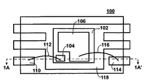
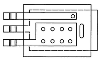
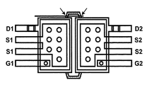
図1は、パワーMOSFETダイを内蔵する従来のパッケージの概略平面図を示している。図1Aは、1A〜1A’線に沿って切断された図1のパッケージの概略断面図を示している。
FIG. 1 shows a schematic plan view of a conventional package incorporating a power MOSFET die. FIG. 1A shows a schematic cross-sectional view of the package of FIG. 1 taken along
特に、従来のパワーMOSFETパッケージ100は、上部表面を有するとともに、ゲートパッド104とソースパッド106を有することを特徴とするパワーMOSFETダイ102を有している。ゲートパッド104は、ボンディングワイヤ112を介して第1のリード110と電気的に接続され、ソースパッド106は、ボンディングワイヤ116を介して第2のリード114と電気的に接続される。
In particular, the conventional
ダイ102の底部表面は、ドレインパッド108を備えることを特徴とする。ドレインパッド108は、電気伝導性接着材120を介して、基盤となるダイパッド118と電気的に接続される。この接着材120には熱伝導性もあるので、作動時にMOSFETダイによって発生する熱は、ダイパッドの下部表面で形成されるヒートシンク122を介して、パッケージの外に輸送される。前記ダイパッドと一体化された各リードを介して、熱エネルギーがパッケージの外に導かれる可能性もある。
The bottom surface of the die 102 is characterized by a
図1乃至図1Aのパッケージは機能的である反面、いくつかの欠点を提供する可能性がある。1つは、ダイの各パッドまたは表面と各リードの間で、ワイヤボンディングをする必要があることである。具体的には、ボンドワイヤ材は一般に、金、つまり非常に高価な原料から作成されるので、このワイヤボンディングステップには費用がかかる。 While the package of FIGS. 1 to 1A is functional, it may provide several drawbacks. One is the need to wire bond between each pad or surface of the die and each lead. Specifically, this wire bonding step is expensive because bond wire materials are typically made from gold, a very expensive raw material.
また、ワイヤボンディングステップでは、ボンドワイヤを曲げて(歪ませて)、ダイと各リードの端部にある狭小な対象領域に、所定の力で高精度に取り付ける必要があるので、ワイヤボンディングステップを実行することは難しい。歪み状態でのワイヤの破損あるいはワイヤ端部を正確に接合できないことによって、欠陥が高められて、スループットが減少する可能性がある。このステップでのダイにワイヤを取り付ける力が、ダイを傷つける可能性もある。 Also, in the wire bonding step, it is necessary to bend (distort) the bond wire and attach it to the narrow target area at the end of the die and each lead with a predetermined force with high precision. Difficult to implement. Failure of the wire in a strained state or failure to accurately join the wire ends can increase defects and reduce throughput. The force of attaching the wire to the die at this step can also damage the die.
さらに、ソースおよびゲートのボンドワイヤ接続は、パッケージが熱エネルギーを放散させる能力を制限する。特に、ボンドワイヤが少量であれば、パッケージ外に熱を輸送するための熱伝導物質は少量しか提供されない。 In addition, source and gate bond wire connections limit the ability of the package to dissipate thermal energy. In particular, a small amount of bond wire provides only a small amount of thermally conductive material for transporting heat out of the package.
最後に、ボンドワイヤによって提供される横断面は比較的小さいので、ダイと各リード間に低抵抗の接触が確立されることを妨げる可能性がある。低抵抗の接触を確立するための従来の試みは、大抵、より多くのボンドワイヤを用いることに帰着するので、上述のコストの問題を悪化させることになる。さらに、ダイ表面で低抵抗の接触を確立するために、複数のボンドワイヤステッチを使用すれば、複数の取り付けステップが必要となるので、ダイを損傷する危険を再度引き起こす可能性がある。 Finally, the cross-section provided by the bond wire is relatively small and may prevent a low resistance contact from being established between the die and each lead. Conventional attempts to establish a low resistance contact often result in the use of more bond wires, thus exacerbating the above cost problems. Furthermore, using multiple bond wire stitches to establish a low resistance contact on the die surface requires multiple attachment steps, which can again cause the risk of damaging the die.
長いボンドワイヤ、多数のボンドワイヤをダイへの電気接続部として使用することによって、他のデメリットが生じる可能性がある。例えば、ボンドワイヤは、MOSFETのスイッチング動作を妨げる可能性がある、より大きなインダクタンスを提供するかもしれない。また、ボンドワイヤは、非制御の外部インダクタンスまたはインピーダンスをパワーICに付加することもできるが、それを補償する内部の集積回路が必要となるであろう。 The use of long bond wires, multiple bond wires as electrical connections to the die can cause other disadvantages. For example, a bond wire may provide a larger inductance that can interfere with the switching operation of the MOSFET. Bond wires can also add uncontrolled external inductance or impedance to the power IC, but will require an internal integrated circuit to compensate for it.
したがって、本技術分野では、良好な熱伝導性を示すとともに、低コストでの製造が可能な、改良されたパッケージ設計が要求される。 Accordingly, there is a need in the art for an improved package design that exhibits good thermal conductivity and that can be manufactured at low cost.
本発明に係る実施形態は、金属層の間に挟まれたフリップチップダイを特徴とする半導体装置用パッケージに関する。一方の金属層は、ハンダ接点を介してダイ(例えば、ICパッドあるいはMOSFETのゲートまたはソースパッド)の第1の表面で種々のパッドと電気的かつ熱的に接続されるように構成されたリードフレームの各部分を有する。他方の金属層は、ダイの反対側と少なくとも熱的に接続される。本発明に係るパッケージの実施形態は、優れた放熱特性を示し、その上、ワイヤボンディングにかかる費用を抑える。 Embodiments according to the present invention relate to a package for a semiconductor device characterized by a flip chip die sandwiched between metal layers. One metal layer is a lead configured to be electrically and thermally connected to various pads at the first surface of a die (eg, IC pad or MOSFET gate or source pad) via solder contacts. With each part of the frame. The other metal layer is at least thermally connected to the opposite side of the die. Embodiments of the package according to the present invention exhibit excellent heat dissipation characteristics and further reduce the cost of wire bonding.
本発明のこれらの実施形態および他の実施形態は、その特徴およびいくつかの潜在的メリットと同様に、以下の文章と添付の図面と共に、より詳細に記述される。 These and other embodiments of the present invention, as well as their features and some potential benefits, are described in more detail in conjunction with the following text and accompanying drawings.
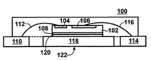
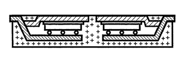
図2は、本発明に係るパッケージの実施形態の概略平面図である。図2Aは、断面線2A−2A’に沿って切り取られた図2のパッケージの概略断面図である。
FIG. 2 is a schematic plan view of an embodiment of a package according to the present invention. 2A is a schematic cross-sectional view of the package of FIG. 2 taken along
パッケージ200は、上部表面にゲートパッド204とソードパッド206を備えることを特徴とするMOSFETダイ202を有する。MOSFETダイ202の底部表面は、ドレイン接点208を備えることを特徴としている。
The
ドレイン接点208は、電気伝導性と熱伝導性を有する接着材220を介して、基盤となる第1の金属層224と電気的に接続される。そのような電気伝導性と熱伝導性を有する材料の一例は、ハンダである。ある実施形態では、第1の金属層は、事前にバンプされたハンダボールが備えられてもよく、あるいは事前に成形されたハンダ付け可能な接触表面が備えられてもよい。
The
第1の金属層224の一体となった各突出部は、それぞれ電気接触用のリードをMOSFETのドレインに提供するために、ブラスチックパッケージ体の外部に延びている。パッケージ体によって露出された第1の金属層224の下側部分は、ヒートシンクとして使用されてもよい。
Each protrusion integrated with the
パッケージ200は、ダイを被覆する第2の金属層226を有する。第2の金属層226の第1の部分228は、ハンダ接続部230を介して、ゲートパッド204と電気的に接続される。第2の金属層226の第2の部分232は、複数のハンダ接続部234を介して、ソースパッド206と電気的に接続される。金属層226の上部部分228および232は、順に配設されて、プラスチックパッケージ体の外部に延びて、ゲートおよびソースに接続するリードとして使用される。この形成工程では、第1の金属層224の高さに適合させるために、第2の金属層226の部分228と232の垂直方向の高さを変えてもよい。ある特定の実施形態では、第2の金属層の形状は、曲げによって形成されてもよい。他の実施形態では、第2の金属層は、事前に成形された形状で提供されてもよい。
The
図2〜図2Aのパッケージ構造は、従来のパッケージ構造を超える多くの利点を提供できる。1つの利点は、製造の間、ワイヤボンディングを必要としないことである。その代わりに、ダイと第2の金属層の間の接触は、曲げと金属ボンドワイヤを正確に整合することを必要としないハンダ接点によって行われる。ワイヤボンディングに代えてそのようなハンダ接点を使用することにより、欠陥の発生が減少するので、パッケージを製造する総コストは減少する。 The package structure of FIGS. 2-2A can provide many advantages over conventional package structures. One advantage is that no wire bonding is required during manufacturing. Instead, the contact between the die and the second metal layer is made by a solder contact that does not require precise alignment of the bend and metal bond wire. By using such solder contacts instead of wire bonding, the total cost of manufacturing the package is reduced because the occurrence of defects is reduced.
本発明の実施形態によれば、好適な電気的性能を提供することもできる。例えば、各ボンドワイヤに関連する各金属層でのインダクタンスを減少すれば、インダクタンスが減少するので、スイッチング速度をより速くできる。細長いボンドワイヤに代えて金属層を用いるので、パッケージに内蔵されたダイへの接触抵抗が、好適に減少される。 According to the embodiment of the present invention, suitable electrical performance can also be provided. For example, if the inductance in each metal layer associated with each bond wire is reduced, the inductance is reduced, so that the switching speed can be increased. Since a metal layer is used in place of the elongated bond wire, the contact resistance to the die embedded in the package is preferably reduced.
図2〜図2Aで示されるパッケージの実施形態によって提供可能な別の利点は、熱を放散させる能力が向上することである。特に、下部金属層は、ダイのドレイン接点と熱的に接続されるので、各リードを介してパッケージの外に熱を伝導できる。そして、ある実施形態では、下部金属層の一部は、パッケージの外部で露出されているので、周辺の環境に対するヒートシンクとして使用される。 Another advantage that can be provided by the package embodiment shown in FIGS. 2-2A is an increased ability to dissipate heat. In particular, the lower metal layer is thermally connected to the drain contact of the die so that heat can be conducted out of the package through each lead. In some embodiments, a portion of the lower metal layer is exposed outside the package and is used as a heat sink for the surrounding environment.
さらに、上部金属層は、ハンダ接続部を介して、ダイの大部分の領域、特に、ダイの上部表面にあるソースパッドと十分に熱的に接触する。このダイの大部分に接触する領域は、各リードを介して、パッケージから離れたダイから周辺の環境への熱の流れをさらに高める。そして、ある実施形態では、上部金属層の一部は、パッケージの外部に露出されているので、周辺の環境に対するヒートシンクとして使用される。 Furthermore, the upper metal layer is in sufficient thermal contact with the majority of the area of the die, particularly the source pad on the upper surface of the die, via the solder connection. The area in contact with the majority of this die further increases the heat flow from the die away from the package to the surrounding environment via each lead. In some embodiments, a portion of the upper metal layer is exposed to the outside of the package and is used as a heat sink for the surrounding environment.
図2〜図2Aに示す実施形態は、ハンダボールを使用して、ダイの片側だけと電気的に接続することを示しているが、このことは本発明にとって必須のものではない。他の実施形態によれば、ハンダボールを使用して、ダイの両側で接点と電気的に接続することもできる。 Although the embodiment shown in FIGS. 2-2A shows using solder balls to make electrical connections to only one side of the die, this is not essential to the invention. According to other embodiments, solder balls can be used to electrically connect contacts on both sides of the die.
そして、図2〜図2Aに示す実施形態は、ドレインと接触する下部金属層およびハンダ接続を介してゲート/ソースと接触する上部金属層を示しているが、このことは本発明にとって必須のものではない。これに替えて、ダイのソースおよびゲートと接触する下部金属層を有することを特徴とするとともに、ドレインと接触する上部金属層を有することを特徴としてもよい。そのような実施形態は、図2Bの概略断面図で示されている。さらに、両金属層によって、望ましい高熱伝導特性と信頼性および製造コストの低下がもたらされる。 The embodiment shown in FIGS. 2 to 2A shows a lower metal layer in contact with the drain and an upper metal layer in contact with the gate / source via a solder connection, which is essential for the present invention. is not. Alternatively, it may be characterized by having a lower metal layer in contact with the source and gate of the die and an upper metal layer in contact with the drain. Such an embodiment is shown in the schematic cross-sectional view of FIG. 2B. In addition, both metal layers provide desirable high thermal conductivity properties and reliability and reduced manufacturing costs.
さらに、図2Cは、本発明に係るパッケージの別の実施形態の概略断面図を示している。この特定の実施形態では、下部金属層は、上部金属層の一部と接触するように、上向きに曲げられており、上部金属層自体は、パッケージ体から外に延びるように、下向きに曲がっている。図2Cの実施形態によれば、第1の金属層の上向きに突出した部分が、パッケージのプラスチック体中に確実に埋設されて、そこに留まるという利点が示される。さらに、図2Cの構造は、正方形または長方形の外形を有するヒートシンクを示している。このようなパッケージの底部に露出する下部金属層の一体化された部分は、パッケージの側面まで延び続けることはない。 Further, FIG. 2C shows a schematic cross-sectional view of another embodiment of a package according to the present invention. In this particular embodiment, the lower metal layer is bent upward to contact a portion of the upper metal layer, and the upper metal layer itself is bent downward to extend out of the package body. Yes. The embodiment of FIG. 2C shows the advantage that the upwardly protruding part of the first metal layer is securely embedded in the plastic body of the package and remains there. Further, the structure of FIG. 2C shows a heat sink having a square or rectangular profile. The integrated portion of the lower metal layer exposed at the bottom of such a package does not continue to extend to the side of the package.
プラスチックのパッケージ体中でダイを封止することに加えて、図2Cのパッケージは、露出されたリードを打ち抜くことによって、周りの材料から個片化される。このようにリードのパッケージ体から外に延びる部分は、テストに供される。この実施形態に代えて、リードの露出部分をパッケージの表面とともに取り除くソーイング工程によって、パッケージを周りの材料から個片化することもできる。 In addition to sealing the die in a plastic package body, the package of FIG. 2C is singulated from the surrounding material by punching the exposed leads. The portion of the lead that extends out from the package body is used for the test. As an alternative to this embodiment, the package can be singulated from the surrounding material by a sawing process that removes the exposed portions of the leads along with the surface of the package.
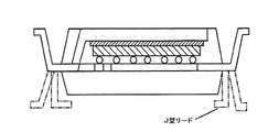
図2Dは、本発明に係るパッケージのさらに別の実施形態の概略断面図を示している。この特定の実施形態では、第1および第2の金属層が、パッケージの厚さの中間点から突出するように構成される。そのような構成によって、パッケージは実用上十分な柔軟性を備えるので、その柔軟性によって、リードの突出部は、パッケージが最終的に設置される環境の要求に応じて、いずれかの方向(上方または下方)および種々の形態(J型、ガルウイング型、逆ガルウイング型)に曲げることができる。 FIG. 2D shows a schematic cross-sectional view of yet another embodiment of a package according to the present invention. In this particular embodiment, the first and second metal layers are configured to protrude from a midpoint of the package thickness. With such a configuration, the package has sufficient practical flexibility, so that the lead protrusions can be oriented in either direction (upward) depending on the requirements of the environment where the package will eventually be installed. Or downward) and various forms (J-shaped, gull-wing, inverted gull-wing).
図2DAは、本発明に係るパッケージのさらに別の実施形態の概略断面図を示している。この実施形態は、パッケージの頂部に配置されたヒートシンクに向けて上方に突出したガルウイング型リードをなすリードを示している。 FIG. 2DA shows a schematic cross-sectional view of yet another embodiment of a package according to the present invention. This embodiment shows a lead that forms a gull-wing lead projecting upward toward a heat sink disposed at the top of the package.
図2E〜図2EAは、本発明に係るパッケージの別の実施形態の概略平面図および断面図を、それぞれ示している。図2E〜図2EAのパッケージは、パッケージの一方の側だけからリードが突出している。第1の突出リードは、パッケージの中間厚さに置かれた下部金属層の一部から形成され、その下部金属層は、ハンダ接点を介してダイのソースパッドと接触している。第2の突出リードも、下部金属層の一部から形成され、その下部金属層は、ハンダ接点を介してダイのゲートパッドと接触している。第3の突出リードは、上部金属層の一部から形成され、その上部金属層は下方向に曲げられてから、パッケージの中間厚さにおいて、パッケージ体の外部に突出する。また、この上部金属層は、ダイのドレインパッドと接触する。図2Eで示されるように、上部金属層は、パッケージ体のプラスチック封止材の侵入を可能にする開孔部を有していてもよく、それによって、パッケージ内での上部金属層の機械的噛み合いが助長される。 2E to 2EA show a schematic plan view and a cross-sectional view, respectively, of another embodiment of a package according to the present invention. In the package of FIGS. 2E to 2EA, the leads protrude from only one side of the package. The first protruding lead is formed from a portion of the lower metal layer placed at the intermediate thickness of the package, and the lower metal layer is in contact with the source pad of the die via a solder contact. The second protruding lead is also formed from a portion of the lower metal layer, and the lower metal layer is in contact with the gate pad of the die through the solder contact. The third protruding lead is formed from a part of the upper metal layer, and the upper metal layer is bent downward and then protrudes outside the package body at the intermediate thickness of the package. The upper metal layer also contacts the drain pad of the die. As shown in FIG. 2E, the upper metal layer may have an opening that allows the plastic sealant of the package body to penetrate, thereby mechanically moving the upper metal layer within the package. Engagement is encouraged.
これまでに記載された実施形態は、3つの端子(ゲート、ソース、ドレイン)を有するMOSFET装置を内蔵するパッケージに関するものである。もっとも、本発明は、この種のダイを内蔵することに限定されない。本発明に係るパッケージの代わりの実施形態は、より少数あるいは多数の端子を有するダイを内蔵するように構成されてもよい。 The embodiments described so far relate to a package containing a MOSFET device having three terminals (gate, source, drain). However, the present invention is not limited to incorporating this type of die. Alternative embodiments of packages according to the present invention may be configured to incorporate dies having fewer or more terminals.
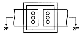
例えば、図2FA〜図2FBは、本発明の実施形態に係る平面2端子素子(例えば、ダイオード)用のリードフレームの平面図および2F−2F’線に沿った断面図を示している。リードフレームは、ダイの裏面だけと熱的に接続される下部金属層を有している。上部金属層の2つの部分は、ダイの上部側で各接点と電気的に接続される。
For example, FIGS. 2FA to 2FB show a plan view of a lead frame for a planar two-terminal element (e.g., a diode) according to an embodiment of the present invention and a cross-sectional view taken along
同様に、図2GA〜図2GBは、本発明の実施形態に係る水平方向の2端子素子(例えば、ダイオード)用のリードフレームの平面図および2G−2G’線に沿った断面図を示している。リードフレームは、ダイの裏面側で接点と電気的に接続される下部金属層とダイの表面側で接点と電気的に接続される上部金属層を有する。
Similarly, FIGS. 2GA to 2GB show a plan view of a lead frame for a horizontal two-terminal element (for example, a diode) according to an embodiment of the present invention and a cross-sectional view taken along
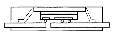
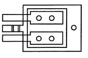
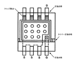
図2Hは、デュアル素子用パッケージ用のリードフレームの平面図を示しているが、このリードフレームは、3つの端子を有しており、そのうちの2つは素子の同一部分に接続されている。特に、下部金属層は、裏面側接点と電気的に接続されており、上部金属層は、それぞれ表面側接点と電気的に接続される2つの部分に別れる。図2Hで示される特定のパッケージは、TO220/247/251型パッケージであり、支持構造にパッケージを固定するネジを収容するタグ孔を備えることを特徴とする。TO263/252型パッケージを含む他の実施形態では、曲げられたり、あるいは、ドレインのヒートシンクと同一平面をなすように事前に成形されたプラスチック体に外部リードを備える。 FIG. 2H shows a plan view of a lead frame for a dual device package, the lead frame having three terminals, two of which are connected to the same part of the device. In particular, the lower metal layer is electrically connected to the back surface side contact, and the upper metal layer is divided into two parts each electrically connected to the front surface side contact. The particular package shown in FIG. 2H is a TO220 / 247/251 type package, characterized in that it includes a tag hole that accommodates a screw that secures the package to the support structure. In other embodiments, including a TO263 / 252 type package, external leads are provided in a plastic body that is bent or pre-shaped to be flush with the drain heat sink.
いま述べたパッケージとリードフレームの実施形態は、単一のダイとして設計されているが、このことは本発明にとって必須のものではない。本発明に係る実施形態ではこれに代えて、複数のダイを内蔵するように構成されてもよい。 Although the package and leadframe embodiments just described are designed as a single die, this is not essential to the invention. Instead of this, the embodiment according to the present invention may be configured to incorporate a plurality of dies.
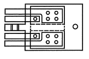
例えば、図2IA〜図2IBは、本発明に係るリードフレームの実施形態の概略平面図および2I−2I’線に沿った断面図を示しており、2つのデュアルダイを内蔵するように構成される。この特定の実施形態では、2つのダイは、共通の裏面側接点用の同一の端子を共有するとともに、そのダイの表面側に別の端子と接点を備える。 For example, FIGS. 2IA-2IB show a schematic plan view and a cross-sectional view along line 2I-2I ′ of an embodiment of a lead frame according to the present invention, which is configured to incorporate two dual dies. . In this particular embodiment, the two dies share the same terminal for a common backside contact and have separate terminals and contacts on the front side of the die.
図2Jは、本発明に係るリードフレームの実施形態の概略平面図を示しており、2つのMOSFETダイを内蔵するように構成されている。この特定の実施形態では、2つのMOSFETダイは、共通の裏面側接点(ドレイン)用の同一の端子を共有するとともに、そのダイの表面側にソース用およびゲート用の端子と接点を備える。 FIG. 2J shows a schematic plan view of an embodiment of a lead frame according to the present invention, which is configured to incorporate two MOSFET dies. In this particular embodiment, the two MOSFET dies share the same terminal for a common back side contact (drain) and have source and gate terminals and contacts on the front side of the die.
図2Jの実施形態は、ソース、ドレインおよびゲート接点のそれぞれについて、単一の端子を有する構成を示しているが、このことは本発明にとって必須のものではない。図2Kは、ソース(S)およびドレイン(D)用の複数の端子を有するMOSFETダイ用のリードフレームの概略平面図を示している。 Although the embodiment of FIG. 2J shows a configuration having a single terminal for each of the source, drain and gate contacts, this is not essential to the invention. FIG. 2K shows a schematic plan view of a lead frame for a MOSFET die having a plurality of terminals for source (S) and drain (D).
同様に、図2LA〜図2LBは、互いに独立したドレインを有する2つのMOSFETダイのそれぞれについて、複数のソース端子を有するリードフレームについての概略平面および断面図を示している。これらのドレインと接触するリードフレーム部分は、成形ステップ後に(例えば、パンチングよって)切断されるタイバー構造により共に固定される。図2Mは、2つの端子(D1,D2)に接触する1個の共通ドレイン接点および、それぞれのダイに対して複数のソース端子を備えて、2つのダイを支持するリードフレームの単純化された平面図を示す。 Similarly, FIGS. 2LA to 2LB show schematic plan and cross-sectional views of a lead frame having a plurality of source terminals for each of two MOSFET dies having independent drains. The lead frame portions that contact these drains are secured together by a tie bar structure that is cut (eg, by punching) after the molding step. FIG. 2M is a simplified leadframe supporting two dies, with one common drain contact contacting two terminals (D1, D2) and multiple source terminals for each die. A plan view is shown.
同様に、図2Nは、複数のソース端子と、それぞれクリップ接続される複数のドレイン端子を備えるとともに、さらに個片化の間および成形後に、周囲の金属マトリックスから切断されるタイバー接続されることを特徴とするリードフレームの別の実施形態の平面図を示している。図2Oは、一団となったドレイン端子の対をそれぞれに備える複数のMOSFETダイを内蔵するとともに、タイバーを含むリードフレームの別の実施形態の概略平面図を示している。 Similarly, FIG. 2N includes a plurality of source terminals and a plurality of clipped drain terminals, respectively, and is further connected to a tie bar cut from the surrounding metal matrix during singulation and after molding. FIG. 6 shows a plan view of another embodiment of a featured lead frame. FIG. 2O shows a schematic plan view of another embodiment of a lead frame that incorporates a plurality of MOSFET dies each with a group of drain terminals each and that includes a tie bar.
前述の実施形態は、同一の種類のダイを内蔵して構成されるリードフレームとパッケージに関するものであるが、このことは本発明にとって必須のものではない。これに代えて、異なるダイの種類、例えば、MOSFETと集積回路(IC)を内蔵するように構成されてもよい。 Although the foregoing embodiments relate to a lead frame and a package that incorporate the same type of die, this is not essential to the present invention. Alternatively, different die types, for example, MOSFETs and integrated circuits (ICs) may be included.
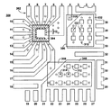
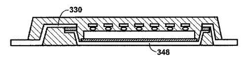
例えば、図3A〜図3Bは、本発明の別の実施形態に係るリードフレーム300の平面図を示している。図3Aは、上部金属層302および3つのパッケージダイ304、306および308の平面図を示している。一方、図3Bは、下部金属層310およびパッケージダイ304、306、308の平面図を示している。図3Cは、概略断面図を示している。
For example, FIGS. 3A-3B show plan views of a
リードフレームの上部金属層302は、内蔵されたダイの上部表面の種々のパッドに接触するリードを有することを特徴とする。例えば、ダイ304は、その上部表面に多くの接点を有するICダイを示している。そのため、リードフレームの上部金属層302は、ダイとの間で必要な電気的かつ熱的な接続を提供するハンダ接点312を介して、これらのパッド上に広がる複数のリード(5番〜17番)を有する。
The
さらに、リードフレームの上部金属層302のリードは、特定の大きさのICダイと接触するものに限定されない。そのため、図3Aに示すように、これらのリードは、より大きなフットプリントを占めるICダイを収容するように、2組のハンダ接点を有する。
Further, the leads of the
対照的に、ダイ306および308は、それぞれの頂部表面にゲートパッドと、それより大きなソースパッドだけを有するMOSFETである。したがって、上部金属層は、各MOSFETダイに対する2つの独立した部分のみを有し、前記部分は、それぞれゲート/ソースパッド上に広がり、ハンダ接点312を介して、それぞれと熱的かつ電気的に接続される。特に、上部金属部分330は、MOSFETダイ306のゲートパッド(4番のリード)と接触しており、大型上部金属部分332は、ダイ306のソースパッド(33〜36番のリード)と接触している。
In contrast, dies 306 and 308 are MOSFETs having only a gate pad and a larger source pad on each top surface. Thus, the top metal layer has only two independent portions for each MOSFET die, each extending over the respective gate / source pad and thermally and electrically connected to each via the
必須ではないが、この特定の実施形態では、大型上部金属部分332は、開孔部333のパターンによって規定される格子様構造を有する。これらの開孔部は、パッケージ内部での温熱環境の変化に対応する収縮と膨張に起因する大型金属部分での熱歪みを低減する。
Although not required, in this particular embodiment, the large
図3Aの実施形態の開孔部は正方形であるが、このことは本発明にとって必須のことではない。これに代えて、特定の用途に応じて、円形や多角形、それ以外の形状を含む他の形状の開孔部を有することを特徴とする金属層を備えることを特徴とすることもできる。 Although the aperture in the embodiment of FIG. 3A is square, this is not essential to the invention. Instead of this, it is also possible to provide a metal layer characterized by having an aperture of another shape including a circular shape, a polygonal shape, or other shapes according to a specific application.
同様に、上部金属層の大型部分340は、MOSFETダイ308のソースパッド(21〜27番のリード)との熱的かつ電気的な接触が可能になっている。図3A〜図3Bに示す実施形態では、上部金属層の同一(幅広)部分(17番のリードに対応する)は、ICとMOSFETダイ308のゲートパッドの双方との共通の接点を有する。
Similarly, the
上部金属層302は、孤立したリード(18〜20番および32番)および一団となったリード(1〜3番および28〜31番)を有すること特徴とする。特に以下で記載されるように、リード1〜3、28〜31および32は、下部金属層を介して、MOSFETダイの下面で、ドレインパッドと電気的に接続される。
The
図3Cの断面図で示されるように、リードフレーム300の上部金属層から延びるリードは、パッケージ体から露出する前に下方向に曲げられて、最終的にパッケージ層の底部から突出する。もっとも、このことは本発明にとって必須のものではない。他の実施形態では、上部金属層は、前に図2Dを引用して示したように、いずれかの方向に曲げられて、パッケージの側部の上部において露出することもできる。
As shown in the cross-sectional view of FIG. 3C, the leads extending from the upper metal layer of the
図3Bに示される下部金属層348の構成は、上部金属層よりも簡単である。ある実施形態では、ICダイ304の基盤となる下部金属層の部分350は、ICダイとは全く電気的に接続されていない。したがって、部分350は、いかなるリードとも接触していない。ただ、ヒートシンクを提供するために、パッケージの底部で露出されているだけである。接地されるとともにピンに接続されるICを要する実施形態では、この例の場合、電気的な接続は、部分350を図3Aのピン5に接続することによって得られる。
The configuration of the
2またはさらに多数のダイの間での接続を要する実施形態では、接続は、適切にパターン化されるとともに、連続するピンに2つ(または複数)のボール接点位置を有することによって提供される。図3Aのピン17は、そのような一例であり、ICとMOSFETのゲートを接続している。
In embodiments that require connection between two or more dies, the connection is provided by having two (or more) ball contact locations on successive pins while being appropriately patterned. The
下部金属層の部分352は、MOSFETダイ306の下面でドレインパッドと電気的かつ熱的に接続される。領域352aは、上部金属層の一団となったピン1〜3および孤立したピン32と接触するように、上方向に湾曲しているので、MOSFETダイ306のドレインとの接触が得られる。下部金属層でのこのような上方向への湾曲は、プラスチックパッケージ体の封止材内の層の機械的噛み合いを提供するのに役立つ。下部金属部分352の下面は、また、パッケージの下面で露出されてヒートシンクとなる。
The lower
下部金属層の部分354は、MOSFETダイ308の下面でドレインパッドと電気的かつ熱的に接続される。部分354aは、上部金属層の一団となったピン28〜31およびピン18と接触するように、上方向に湾曲しているので、MOSFETダイ308のドレインとの接触が得られる。下部金属層でのこのような上方向への湾曲は、プラスチックパッケージ本体の封止材内の層の機械的噛み合いを提供するのに役立つ。下部金属部分354の下面は、また、パッケージの下面で露出されてヒートシンクとなる。
The lower
図3A〜図3Bのパッケージの特定の実施形態では、ピン18番は、実装とMOSFET308のドレインのヒートシンクへの電気的な接続をもたらすのに役立つ。この実施形態では、ピン19番および20番は接続ピンではないが、他の実施形態では、熱的かつ電気的な接続用の予備位置として使用することができる。
In the particular embodiment of the package of FIGS. 3A-3B,
先述のリードフレームの実施形態は、いくつかの利点をもたらす。1つの利点は、構成と大きさの異なるダイを内蔵できる適合性を有することである。例えば、MOSFETダイは、格子様の下部金属部分の利用可能な領域の大部分を占有するように示されているが、このことは必須ではない。図3A〜図3Bに示されるリードフレームの実施形態は、上部金属部分の内部に適合する、より小さなフットプリントあるいは異なるフットプリントを占有するMOSFETダイを内蔵するように構成されてもよい。そのような実施形態では、ある特定の接点(例えば、ゲート)の位置を固定して、他の接点(例えば、ソース)の位置はダイの大きさや形状に応じて空間内で変えられるようにすることもできる。 The lead frame embodiments described above provide several advantages. One advantage is the suitability to accommodate dies of different configurations and sizes. For example, although the MOSFET die is shown to occupy most of the available area of the lattice-like lower metal portion, this is not essential. The lead frame embodiment shown in FIGS. 3A-3B may be configured to incorporate a MOSFET die that occupies a smaller or different footprint that fits inside the upper metal portion. In such an embodiment, the position of one particular contact (eg, gate) is fixed so that the position of the other contact (eg, source) can be changed in space depending on the size and shape of the die. You can also.
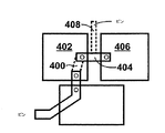
本発明の実施形態に係るパッケージ体からピンとして突出するリードフレームの金属層の部分は、パッケージの内部で作用して、同一水平面上に実装される2または多数の別個のダイの間で、アプリケーションの要求に応じて、信号ルーティング機能を成しうる。例えば、図4は、一実施形態の概略図を示しており、ICダイ401およびMOSFETダイ402は、連続するピンを介してハンダボール接続と結合される。さらに、図4は、ある実施形態に従って、この連続するピン接続が部分400として延長された後、部分404まで達することができることを示しており、このことは、ICダイ402とMOSFETダイ406の接点の間に連続する信号ルーティングを提供する。ある実施形態では、部分404は、突出されたピン部分408として延びている。
A portion of the metal layer of the lead frame that protrudes as a pin from the package body according to the embodiment of the present invention acts inside the package and is applied between two or many separate dies mounted on the same horizontal plane. A signal routing function can be performed according to the request of the user. For example, FIG. 4 shows a schematic diagram of one embodiment, where IC die 401 and MOSFET die 402 are coupled to a solder ball connection via a series of pins. Further, FIG. 4 shows that, in accordance with an embodiment, this continuous pin connection can be extended to
これまでに示された実施形態は、同一の水平面に信号ルーティングで配置された複数のダイを内蔵するように構成されるパッケージとリードフレームを表しているが、このことは本発明にとって必須のものではない。これに代えて、本発明に係るパッケージとリードフレームの実施形態は、垂直方向に積層して配向される多数のダイや他の配向を有することを特徴としてもよい。 Although the embodiments shown so far represent a package and a lead frame configured to incorporate a plurality of dies arranged by signal routing on the same horizontal plane, this is essential for the present invention. is not. Alternatively, embodiments of the package and leadframe according to the present invention may be characterized by having a large number of dies stacked in a vertical direction and other orientations.
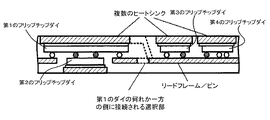
例えば、図5は、2つのフリップチップダイを内蔵して構成されるパッケージの実施形態の概略断面図を示している。第1のフリップチップダイ500は、リードフレームの上部金属層502の下面に支持されている。第2のフリップチップダイ504は、リードフレームの下部金属層506に支持されている。ダイ500と504の表面の接点は、ハンダボール508を介して、互いに電気的に接続されている。第1のダイ500の表面の他の接点は、中間金属層510と電気的に接触している。
For example, FIG. 5 shows a schematic cross-sectional view of an embodiment of a package configured with two flip chip dies built therein. The first flip chip die 500 is supported on the lower surface of the
積層されたダイの構成とは別に、図5の実施形態の2つの態様が注目に値する。第1に、図5のパッケージは、その両側に露出されたヒートシンクを有する。そのようなヒートシンクの1つは、下方に置かれたPCボードと熱的に接続されてもよく、また、周辺の環境と熱的に接続される他方のヒートシンクと熱的に接続されてもよい。先述した1または複数の実施形態に、複数のヒートシンクをそのように使用できることが、理解されるべきである。 Apart from the stacked die configuration, two aspects of the embodiment of FIG. 5 are notable. First, the package of FIG. 5 has heat sinks exposed on both sides thereof. One such heat sink may be thermally connected to the underlying PC board and may be thermally connected to the other heat sink that is thermally connected to the surrounding environment. . It should be understood that a plurality of heat sinks may be used as such in one or more of the previously described embodiments.
第2に、本発明に係る実施形態は、2または任意の数の多数の金属層を使用することに限定されたり、2つのダイのみを含むことに限定されたりしない。むしろ、本発明の実施形態では、任意の数の所望のダイを複数の金属層で挟んで実施することができる。 Second, embodiments according to the present invention are not limited to using two or any number of multiple metal layers, or to including only two dies. Rather, in embodiments of the present invention, any number of desired dies may be sandwiched between multiple metal layers.
図3A〜図3Cに関連して上述されたように、多様な大きさのダイが種々の金属層に支持されることが許されるので、パッケージの設計者は、本発明の実施形態に係るリードフレームを柔軟に設計できる。本発明の実施形態に従うサンドイッチ構造で、複数のモジュールを結合すれば、パッケージ設計が更に柔軟になる。 As described above in connection with FIGS. 3A-3C, various sized dies are allowed to be supported on various metal layers so that package designers can use the leads according to embodiments of the present invention. The frame can be designed flexibly. If a plurality of modules are combined in the sandwich structure according to the embodiment of the present invention, the package design becomes more flexible.
例えば、図6は、図示される第1および第2の金属層604、606の間に挟まれた第1のフリップチップダイ602を含むパッケージ600を示している。マルチチップモジュール(MCM)の製造は、それ自体が金属層612と614の間に挟まれる第2のフリップチップダイ610を含むモジュール609を組み込むことによって達成される。パズルのピースを組み合わせるのと類似する方法で、パッケージが、複数の挟まれたダイ部品から組み立てられることによって、特殊な要求に対するパッケージの設計に、十分な柔軟性を付加することができる。
For example, FIG. 6 shows a
図7は、本発明に係るパッケージのさらに別の実施形態の概略断面図を示しており、この実施形態のパッケージは、複数の小さな要素から形成されている。特に、パッケージは、サンドイッチ状の金属層の一方とのハンダボール接点を介して(例えば、第3のフリップチップダイと第4のフリップチップダイの間の陰をつけられたハンダボールおよび下部金属層を介して)、同一面に内部接続部と信号ルーティングを有するダイを有する。パッケージは、ハンダボール接点を介して(例えば、第1のフリップチップダイと第2のフリップチップダイの間にある陰をつけられたハンダボールを介して)、互いに垂直方向にある内部接続部と信号ルーティングを有するダイも有している。このパッケージでは、サンドイッチ状の下部金属層は、垂直方向に接続されるダイの1つを支持する下部金属層との接続を確立するために、下部平面にあってもよく、あるいは、垂直方向に接続されるダイの上部と接続される上部金属層との接続を確立するために、上方向に曲げられていてもよい。図7のパッケージは、両側にヒートシンクを有しており、上面側に複数のヒートシンクを有している。 FIG. 7 shows a schematic cross-sectional view of yet another embodiment of a package according to the invention, the package of this embodiment being formed from a plurality of small elements. In particular, the package is connected via a solder ball contact with one of the sandwich metal layers (eg, the shaded solder ball and the lower metal layer between the third flip chip die and the fourth flip chip die). Via a die having internal connections and signal routing on the same plane. The package is connected to the interconnects perpendicular to each other via solder ball contacts (eg, via a shaded solder ball between the first flip chip die and the second flip chip die). It also has a die with signal routing. In this package, the sandwiched lower metal layer may be in the lower plane to establish a connection with the lower metal layer that supports one of the vertically connected dies, or in the vertical direction. It may be bent upward to establish a connection between the top of the connected die and the top metal layer to be connected. The package in FIG. 7 has heat sinks on both sides, and has a plurality of heat sinks on the upper surface side.
本発明に係る実施形態は、特定の種類のダイを内蔵することに限定されない。もっとも、パワーデバイスのような、ある種のダイは、本発明に係るパッケージに特に適している。本出願の目的において、「パワーデバイス」という用語は、パワーエレクトロニクス回路の中でスイッチまたは整流器として使用される半導体装置について言及していると解釈される。これらは、ダイオード、パワーMOSFET、絶縁ゲート型バイポーラ・トランジスタ(IGBT)、ディスクリートデバイスのアナログまたはデジタル制御に用いられるパワー集積回路のようなディスクリートデバイスを含むが、これらに限定されない。 Embodiments according to the present invention are not limited to incorporating a particular type of die. However, certain dies, such as power devices, are particularly suitable for packages according to the present invention. For the purposes of this application, the term “power device” is taken to refer to a semiconductor device used as a switch or rectifier in a power electronics circuit. These include, but are not limited to, discrete devices such as diodes, power MOSFETs, insulated gate bipolar transistors (IGBTs), and power integrated circuits used for analog or digital control of discrete devices.
パワーデバイスは、組み合わされて、電源や蓄電制御システムのような電力操作機能を発揮するように一般に用いられる。平面あるいは垂直構造を有するパワーディスクリートデバイスは、数ミリワットから数キロワットまでの電力を処理できる。上述したパッケージに対して、典型的なパワーデバイスが、約500ワットと5ミリワットの間で操作されてもよい。オフ状態では、約数ボルトから約2000ボルトまでの電圧で逆降伏が起こる可能性がある。パワーデバイス用の操作電流は、数ミリアンペアから数百アンペアまでの範囲に亘る可能性がある。 In general, power devices are used in combination so as to exhibit a power operation function such as a power source and a power storage control system. A power discrete device having a planar or vertical structure can handle power from several milliwatts to several kilowatts. For the packages described above, a typical power device may be operated between about 500 watts and 5 milliwatts. In the off state, reverse breakdown can occur at voltages from about a few volts to about 2000 volts. The operating current for power devices can range from a few milliamps to hundreds of amps.
上記は、特定の実施形態の詳細な記載であるが、種々の修正例、代替構造および均等物が用いられてもよい。したがって、上記の記載および説明は、添付された請求項によって定義される本発明の範囲を限定するものと解されるべきではない。 While the above is a detailed description of particular embodiments, various modifications, alternative constructions and equivalents may be used. Therefore, the above description and description should not be taken as limiting the scope of the invention which is defined by the appended claims.
本特許出願は、2008年5月15日提出の米国仮特許出願第61/053,561号および、2008年8月5日提出の米国特許出願第12/186,342号に基づく優先権を主張するものであり、その全てが、全ての目的において参照されて、本特許出願に包含される。 This patent application claims priority based on US Provisional Patent Application No. 61 / 053,561 filed May 15, 2008 and US Patent Application No. 12 / 186,342 filed August 5, 2008. All of which are hereby incorporated by reference for all purposes.
Claims (33)
前記パワーデバイスダイの前記第1の金属層の配置された側の反対側に配置される第2の金属層と、からなる半導体装置用パッケージにおいて、
前記第2の金属層は、前記パワーデバイスダイの表面で、ハンダボール接点を介してパッドと電気的かつ熱的に接続されるように構成され、
前記第1の金属層または前記第2の金属層は、前記パワーデバイスダイ、前記ハンダボール接点および前記第1および第2の金属層の少なくとも一部を封止するプラスチックパッケージ体から突出する一体型のリードを有する
ことを特徴とする半導体装置用パッケージ。 A first metal layer configured to be thermally connected to the power device die;
A package for a semiconductor device comprising: a second metal layer disposed on an opposite side of the power device die to the side on which the first metal layer is disposed;
The second metal layer is configured to be electrically and thermally connected to a pad via a solder ball contact on a surface of the power device die;
The first metal layer or the second metal layer protrudes from a plastic package body that seals at least a part of the power device die, the solder ball contact, and the first and second metal layers. A package for a semiconductor device, characterized by having a lead.
ことを特徴とする請求項1に記載の半導体装置用パッケージ。 The package for a semiconductor device according to claim 1, wherein the first metal layer is electrically connected to the power device die.
ことを特徴とする請求項2に記載の半導体装置用パッケージ。 The package for a semiconductor device according to claim 2, wherein the first metal layer is electrically connected to the power device die through a second solder ball contact.
ことを特徴とする請求項1に記載の半導体装置用パッケージ。 The semiconductor device package according to claim 1, wherein a part of the first metal layer is exposed from the plastic package body to form a heat sink.
ことを特徴とする請求項1に記載の半導体装置用パッケージ。 The semiconductor device package according to claim 1, wherein a part of the second metal layer is exposed from the plastic package body to form a heat sink.
ことを特徴とする請求項1に記載の半導体装置用パッケージ。 The package for a semiconductor device according to claim 1, further comprising a second power device die electrically connected to a part of the second metal layer.
ことを特徴とする請求項6に記載の半導体装置用パッケージ。 The semiconductor device package according to claim 6, wherein the same portion of the second metal layer is electrically connected to the first power device die and the second power device die.
ことを特徴とする請求項7に記載の半導体装置用パッケージ。 The package for a semiconductor device according to claim 7, wherein the same portion of the second metal layer is electrically connected to the first metal layer in a vertical direction.
前記第2の金属層の同一部分は、前記第1のパワーデバイスダイと電気的に接続される
ことを特徴とする請求項7に記載の半導体装置用パッケージ。 The first power device die is a MOSFET;
The package for a semiconductor device according to claim 7, wherein the same portion of the second metal layer is electrically connected to the first power device die.
第1のパワーデバイスダイの大きさや形状によって、異なる位置で前記第1のパワーデバイスチップに対するその他のハンダボール接点を受容するように構成される
ことを特徴とする請求項6に記載の半導体装置用パッケージ。 The second metal layer is configured to receive the solder ball contact in a fixed position;
7. The semiconductor device according to claim 6, wherein the solder ball contact is configured to receive another solder ball contact with respect to the first power device chip at a different position depending on the size or shape of the first power device die. package.
ハンダボールを介して、前記第2のパワーデバイスダイのパッドと電気的に接続されるパッドを有する
ことを特徴とする請求項6に記載の半導体装置用パッケージ。 And further including a third power device die disposed above or below the second die,
The package for a semiconductor device according to claim 6, further comprising a pad electrically connected to a pad of the second power device die through a solder ball.
前記第2の金属層は、前記MOSFETダイの表面でゲートパッドと電気的に接続される第1の部分と前記MOSFETダイの表面でソースパッドと電気的に接続される第2の部分を有する
ことを特徴とする請求項1に記載の半導体装置用パッケージ。 The power device die includes a MOSFET die,
The second metal layer has a first portion electrically connected to the gate pad on the surface of the MOSFET die and a second portion electrically connected to the source pad on the surface of the MOSFET die. The package for a semiconductor device according to claim 1.
ことを特徴とする請求項12に記載の半導体装置用パッケージ。 The package for a semiconductor device according to claim 12, wherein the first metal layer is thermally and electrically connected to a drain on a second surface of the MOSFET die.
ことを特徴とする請求項12に記載の半導体装置用パッケージ。 The package for a semiconductor device according to claim 12, wherein the lead is integrated with the second metal layer.
前記第2の金属層は、前記ICダイの表面で各パッドと電気的に接続される複数の部分を含む
ことを特徴とする請求項1に記載の半導体装置用パッケージ。 The power device die includes an integrated circuit (IC) die;
The package for a semiconductor device according to claim 1, wherein the second metal layer includes a plurality of portions electrically connected to the pads on the surface of the IC die.
ことを特徴とする請求項15に記載の半導体装置用パッケージ。 The package for a semiconductor device according to claim 15, wherein the first metal layer is electrically connected to the second surface of the IC die.
ことを特徴とする請求項1に記載の半導体装置用パッケージ。 The package for a semiconductor device according to claim 1, wherein a part of the second metal layer includes an opening portion.
前記第1のパワーデバイスダイの上方または下方に配置されるとともに、ハンダボール接点を介して、前記第1のパワーデバイスダイの第2の側面と電気的に接触する第2のパワーデバイスダイと、
前記第1のパワーデバイスダイから前記第2のパワーデバイスダイの対向する側に配置される第2の金属層と、から構成される半導体装置用パッケージであって、
前記第2の金属層は、前記第2のパワーデバイスダイと少なくとも熱的に接続され、
前記第1の金属層または前記第2の金属層は、前記パワーデバイスダイと、前記ハンダボール接点と、前記第1および第2の金属層の少なくとも一部を封止するプラスチックパッケージ体から突出する一体型のリードを有し、
前記第1のパワーデバイスダイまたは前記第2のパワーデバイスダイは、前記第1の金属層または前記第2の金属層と電気的に接続される
ことを特徴とする半導体装置用パッケージ。 A first metal layer at least thermally connected to the first side of the first power device die;
A second power device die disposed above or below the first power device die and in electrical contact with a second side of the first power device die via a solder ball contact;
A package for a semiconductor device comprising: a second metal layer disposed on the opposite side of the second power device die from the first power device die;
The second metal layer is at least thermally connected to the second power device die;
The first metal layer or the second metal layer protrudes from the power device die, the solder ball contact, and a plastic package that seals at least a portion of the first and second metal layers. With integrated leads,
The package for a semiconductor device, wherein the first power device die or the second power device die is electrically connected to the first metal layer or the second metal layer.
ことを特徴とする請求項18に記載の半導体装置用パッケージ。 The package for a semiconductor device according to claim 18, wherein the first power device die is electrically connected to the first metal layer via a second solder ball contact.
ことを特徴とする請求項18に記載の半導体装置用パッケージ。 The first power device die is electrically connected to a third metal layer disposed between the first and second metal layers via a second solder ball contact. The package for a semiconductor device according to claim 18.
ことを特徴とする請求項18に記載の半導体装置用パッケージ。 The semiconductor device package according to claim 18, wherein a part of the first metal layer is exposed from the plastic package body to form a heat sink.
ことを特徴とする請求項18に記載の半導体装置用パッケージ。 The package for a semiconductor device according to claim 18, wherein a part of the second metal layer is exposed from the plastic package body to form a second heat sink.
ハンダボール接点を介して、前記第1の表面に対向する前記パワーデバイスチップの第2の表面と熱的かつ電気的に接続される第2の金属層を備える工程と、
前記ダイ、前記ハンダボール接点、および前記第1および第2の金属層の少なくとも一部をプラスチック封止材の内部で封止して、パッケージ体を形成する工程と、を有する
ことを特徴とする半導体装置のパッケージ方法。 Providing a first metal layer that is at least thermally connected to the first surface of the power device die;
Providing a second metal layer that is thermally and electrically connected to the second surface of the power device chip opposite the first surface via a solder ball contact;
Forming a package body by sealing at least a part of the die, the solder ball contact, and the first and second metal layers inside a plastic sealing material. Semiconductor device packaging method.
ことを特徴とする請求項23に記載の半導体装置のパッケージ方法。 The method for packaging a semiconductor device according to claim 23, wherein the first metal layer is electrically connected to the power device die.
ことを特徴とする請求項23に記載の半導体装置のパッケージ方法。 The method of packaging a semiconductor device according to claim 23, wherein the step of sealing the power device die is a step of exposing a part of the first metal layer as a heat sink.
ことを特徴とする請求項23に記載の半導体装置のパッケージ方法。 The method for packaging a semiconductor device according to claim 23, wherein the step of sealing the power device die is a step of exposing a part of the second metal layer as a second heat sink.
ことを特徴とする請求項23に記載の半導体装置のパッケージ方法。 24. The method according to claim 23, further comprising: forming a lead by bending a part of the second metal layer out of a plane of the second metal layer and exposing the second metal layer from the package body. Semiconductor device packaging method.
ことを特徴とする請求項23に記載の半導体装置のパッケージ方法。 24. The semiconductor device according to claim 23, wherein a lead is formed by providing a bent portion outside the plane of the second metal layer in the second metal layer and exposing the second metal layer from the package body. Packaging method.
前記第2の金属層は、ハンダボール接点を介して、前記第1の表面に対向する前記第2のパワーデバイスダイの第2の表面で、各パッドと電気的かつ熱的に接続される部分を有する
ことを特徴とする請求項23に記載の半導体装置のパッケージ方法。 The first metal layer comprises a portion that is at least thermally connected to the first surface of the second power device die;
The second metal layer is a portion electrically and thermally connected to each pad on the second surface of the second power device die facing the first surface via a solder ball contact. 24. The method of packaging a semiconductor device according to claim 23, wherein:
ことを特徴とする請求項29に記載の半導体装置のパッケージ方法。 30. The method of packaging a semiconductor device according to claim 29, wherein the portion is also electrically connected to a pad at the second surface of the first power device die.
前記部分を、前記MOSFETダイのゲートと電気的に接続する
ことを特徴とする請求項29に記載の半導体装置のパッケージ方法。 The first power device die has a MOSFET die;
30. The method of packaging a semiconductor device according to claim 29, wherein the portion is electrically connected to a gate of the MOSFET die.
ことを特徴とする請求項29に記載の半導体装置のパッケージ方法。 And a third power device die that is exposed above or below the second power device die and electrically connected to the second power device die via a second solder ball contact. The method for packaging a semiconductor device according to claim 29, further comprising a step of providing the semiconductor device.
前記第1のパワーデバイスダイの上方または下方に配置されるとともに、ハンダボール接点を介して、前記第1のパワーデバイスダイの第2の側面と電気的に接触する第2のパワーデバイスダイを備える工程と、
前記第1のパワーデバイスダイから前記第2のパワーデバイスダイの対向する側に配置される第2の金属層を備える工程と、を有する半導体装置用パッケージの形成方法において、
前記第2の金属層は、前記第2のパワーデバイスダイと少なくとも熱的に接続され、
前記第1の金属層または前記第2の金属層は、前記パワーデバイスダイと前記ハンダボール接点と前記第1および第2の金属層の少なくとも一部を封止するプラスチックパッケージ体から突出する一体型のリードを有し、
前記第1のパワーデバイスダイまたは前記第2のパワーデバイスダイを、前記第1の金属層または前記第2の金属層と電気的に接続する
ことを特徴とする半導体装置用パッケージの形成方法。 Providing a first metal layer configured to be at least thermally connected to a first side of a first power device die;
A second power device die disposed above or below the first power device die and in electrical contact with a second side surface of the first power device die via a solder ball contact; Process,
A step of providing a second metal layer disposed on the opposite side of the second power device die from the first power device die.
The second metal layer is at least thermally connected to the second power device die;
The first metal layer or the second metal layer protrudes from a plastic package body that seals at least a part of the power device die, the solder ball contact, and the first and second metal layers. With a lead
A method for forming a package for a semiconductor device, wherein the first power device die or the second power device die is electrically connected to the first metal layer or the second metal layer.
Applications Claiming Priority (2)
| Application Number | Priority Date | Filing Date | Title |
|---|---|---|---|
| US5356108P | 2008-05-15 | 2008-05-15 | |
| US12/186,342 US8358017B2 (en) | 2008-05-15 | 2008-08-05 | Semiconductor package featuring flip-chip die sandwiched between metal layers |
Publications (2)
| Publication Number | Publication Date |
|---|---|
| JP2009278103A true JP2009278103A (en) | 2009-11-26 |
| JP2009278103A5 JP2009278103A5 (en) | 2012-06-28 |
Family
ID=41315409
Family Applications (1)
| Application Number | Title | Priority Date | Filing Date |
|---|---|---|---|
| JP2009116937A Pending JP2009278103A (en) | 2008-05-15 | 2009-05-13 | Semiconductor package featuring flip-chip die sandwiched between metal layers |
Country Status (3)
| Country | Link |
|---|---|
| US (2) | US8358017B2 (en) |
| JP (1) | JP2009278103A (en) |
| CN (1) | CN101582403B (en) |
Cited By (6)
| Publication number | Priority date | Publication date | Assignee | Title |
|---|---|---|---|---|
| JP2013152983A (en) * | 2012-01-24 | 2013-08-08 | Toyota Motor Corp | Method of manufacturing semiconductor device |
| KR101367065B1 (en) | 2012-10-30 | 2014-02-24 | 삼성전기주식회사 | Power module package |
| KR101652423B1 (en) * | 2016-07-07 | 2016-08-30 | 제엠제코(주) | Finger clip bonded semiconductor package |
| WO2019159576A1 (en) * | 2018-02-13 | 2019-08-22 | 日立オートモティブシステムズ株式会社 | Electronic control device |
| JP2019186321A (en) * | 2018-04-05 | 2019-10-24 | ローム株式会社 | Semiconductor device |
| WO2022196453A1 (en) * | 2021-03-18 | 2022-09-22 | 株式会社デンソー | Semiconductor module and electronic device using same |
Families Citing this family (50)
| Publication number | Priority date | Publication date | Assignee | Title |
|---|---|---|---|---|
| JPWO2010004609A1 (en) * | 2008-07-07 | 2011-12-22 | 三菱電機株式会社 | Power semiconductor device |
| US8168490B2 (en) | 2008-12-23 | 2012-05-01 | Intersil Americas, Inc. | Co-packaging approach for power converters based on planar devices, structure and method |
| US8673687B1 (en) * | 2009-05-06 | 2014-03-18 | Marvell International Ltd. | Etched hybrid die package |
| US8178954B2 (en) * | 2009-07-31 | 2012-05-15 | Alpha & Omega Semiconductor, Inc. | Structure of mixed semiconductor encapsulation structure with multiple chips and capacitors |
| US8648458B2 (en) * | 2009-12-18 | 2014-02-11 | Nxp B.V. | Leadframe circuit and method therefor |
| TWI453831B (en) | 2010-09-09 | 2014-09-21 | 台灣捷康綜合有限公司 | Semiconductor package and method for making the same |
| JP2012089563A (en) * | 2010-10-15 | 2012-05-10 | Sanken Electric Co Ltd | Semiconductor module |
| JP5921072B2 (en) * | 2011-03-05 | 2016-05-24 | 新電元工業株式会社 | Resin-sealed semiconductor device |
| EP2482312A4 (en) * | 2011-04-29 | 2012-09-26 | Huawei Tech Co Ltd | Power supply module and packaging and integrating method thereof |
| US8310098B2 (en) | 2011-05-16 | 2012-11-13 | Unigen Corporation | Switchable capacitor arrays for preventing power interruptions and extending backup power life |
| CN102201449B (en) * | 2011-05-27 | 2013-01-09 | 电子科技大学 | Low-heat-resistance packaging structure of power MOS (Metal Oxide Semiconductor) device |
| ITMI20111219A1 (en) | 2011-06-30 | 2012-12-31 | St Microelectronics Srl | SYSTEM WITH SHARED HEAT SINK |
| ITMI20111216A1 (en) | 2011-06-30 | 2012-12-31 | St Microelectronics Srl | ELECTRONIC POWER DEVICE WITH HIGH HEAT DISSIPATION AND STABILITY? |
| ITMI20111214A1 (en) | 2011-06-30 | 2012-12-31 | St Microelectronics Srl | POWER REDUCED THICKNESS DEVICE |
| US8723311B2 (en) * | 2011-06-30 | 2014-05-13 | Stmicroelectronics S.R.L. | Half-bridge electronic device with common heat sink on mounting surface |
| ITMI20111208A1 (en) | 2011-06-30 | 2012-12-31 | St Microelectronics Srl | SYSTEM WITH STABILIZED HEAT SINK |
| ITMI20111218A1 (en) | 2011-06-30 | 2012-12-31 | St Microelectronics Srl | HIGH SPEED POWER DEVICE? OF SWITCHING |
| ITMI20111213A1 (en) | 2011-06-30 | 2012-12-31 | St Microelectronics Srl | SEMI-BRIDGE ELECTRONIC DEVICE WITH COMMON AUXILIARY HEAT SINK |
| ITMI20111217A1 (en) * | 2011-06-30 | 2012-12-31 | St Microelectronics Srl | CONTAINER / SINK SYSTEM FOR ELECTRONIC COMPONENT |
| US9041183B2 (en) * | 2011-07-19 | 2015-05-26 | Ut-Battelle, Llc | Power module packaging with double sided planar interconnection and heat exchangers |
| US9601417B2 (en) * | 2011-07-20 | 2017-03-21 | Unigen Corporation | “L” shaped lead integrated circuit package |
| US20160277017A1 (en) * | 2011-09-13 | 2016-09-22 | Fsp Technology Inc. | Snubber circuit |
| US20140070329A1 (en) | 2012-09-07 | 2014-03-13 | Fairchild Semiconductor Corporation | Wireless module with active and passive components |
| CN103681557B (en) * | 2012-09-11 | 2017-12-22 | 恩智浦美国有限公司 | Semiconductor devices and its assemble method |
| US9966330B2 (en) * | 2013-03-14 | 2018-05-08 | Vishay-Siliconix | Stack die package |
| US9589929B2 (en) | 2013-03-14 | 2017-03-07 | Vishay-Siliconix | Method for fabricating stack die package |
| US9070657B2 (en) | 2013-10-08 | 2015-06-30 | Freescale Semiconductor, Inc. | Heat conductive substrate for integrated circuit package |
| CN103594448A (en) * | 2013-11-15 | 2014-02-19 | 杰群电子科技(东莞)有限公司 | Lead frame |
| US9559064B2 (en) * | 2013-12-04 | 2017-01-31 | Taiwan Semiconductor Manufacturing Company, Ltd. | Warpage control in package-on-package structures |
| FR3023059B1 (en) * | 2014-06-25 | 2018-01-05 | Commissariat A L'energie Atomique Et Aux Energies Alternatives | INTEGRATED CIRCUIT COMPRISING A HEAT SINK |
| US9431319B2 (en) | 2014-08-01 | 2016-08-30 | Linear Technology Corporation | Exposed, solderable heat spreader for integrated circuit packages |
| US9425304B2 (en) | 2014-08-21 | 2016-08-23 | Vishay-Siliconix | Transistor structure with improved unclamped inductive switching immunity |
| CN105489571B (en) * | 2014-09-15 | 2018-04-20 | 万国半导体(开曼)股份有限公司 | A kind of flange-cooled semiconductor packages and its method for packing |
| US10319674B2 (en) * | 2014-10-29 | 2019-06-11 | Infineon Technologies Americas Corp. | Packaged assembly for high density power applications |
| US10685904B2 (en) | 2014-11-21 | 2020-06-16 | Delta Electronics, Inc. | Packaging device and manufacturing method thereof |
| US10535587B2 (en) * | 2015-02-04 | 2020-01-14 | Stmicroelectronics S.R.L. | Integrated electronic device having a dissipative package, in particular dual side cooling package |
| WO2017054855A1 (en) * | 2015-09-30 | 2017-04-06 | Agile Power Switch 3D - Integration Apsi3D | A semiconductor power device comprising additional tracks and method of manufacturing the semiconductor power device |
| WO2017091152A1 (en) * | 2015-11-23 | 2017-06-01 | Agency For Science, Technology And Research | Wafer level integration of high power switching devices on cmos driver integrated circuit |
| US10586757B2 (en) | 2016-05-27 | 2020-03-10 | Linear Technology Corporation | Exposed solderable heat spreader for flipchip packages |
| CN108400117A (en) * | 2017-02-06 | 2018-08-14 | 钰桥半导体股份有限公司 | The heat-dissipating gain-type semiconductor subassembly and preparation method thereof that three-dimensional is integrated |
| CN108400118A (en) * | 2017-02-06 | 2018-08-14 | 钰桥半导体股份有限公司 | The semiconductor subassembly and preparation method thereof that three-dimensional is integrated |
| JP6661565B2 (en) * | 2017-03-21 | 2020-03-11 | 株式会社東芝 | Semiconductor device and manufacturing method thereof |
| CN108133915B (en) * | 2017-12-21 | 2020-04-03 | 乐健科技(珠海)有限公司 | Power module with built-in power device and double-sided heat dissipation function and manufacturing method thereof |
| US10872848B2 (en) * | 2018-10-25 | 2020-12-22 | Infineon Technologies Ag | Semiconductor package with leadframe interconnection structure |
| US11476232B2 (en) | 2019-03-25 | 2022-10-18 | Analog Devices International Unlimited Company | Three-dimensional packaging techniques for power FET density improvement |
| CN112447614A (en) * | 2019-08-30 | 2021-03-05 | 朋程科技股份有限公司 | Power device packaging structure |
| CN111540723A (en) * | 2020-05-06 | 2020-08-14 | 晏新海 | Power semiconductor device |
| KR20220055112A (en) | 2020-10-26 | 2022-05-03 | 삼성전자주식회사 | Semiconductor package including semiconductor chips |
| JP7470086B2 (en) * | 2021-09-13 | 2024-04-17 | 株式会社東芝 | Semiconductor Device |
| CN114730747B (en) * | 2022-02-22 | 2023-04-04 | 香港应用科技研究院有限公司 | Power converter packaging structure of thermally enhanced interposer with cooling fins |
Citations (1)
| Publication number | Priority date | Publication date | Assignee | Title |
|---|---|---|---|---|
| JP2005159238A (en) * | 2003-11-28 | 2005-06-16 | Renesas Technology Corp | Semiconductor device |
Family Cites Families (6)
| Publication number | Priority date | Publication date | Assignee | Title |
|---|---|---|---|---|
| US6191478B1 (en) * | 1999-06-07 | 2001-02-20 | Agilent Technologies Inc. | Demountable heat spreader and high reliability flip chip package assembly |
| US6731000B1 (en) * | 2002-11-12 | 2004-05-04 | Koninklijke Philips Electronics N.V. | Folded-flex bondwire-less multichip power package |
| JP2005302951A (en) * | 2004-04-09 | 2005-10-27 | Toshiba Corp | Semiconductor device package for power |
| CN100390974C (en) * | 2004-08-20 | 2008-05-28 | 清华大学 | Large-area heat sink structure for large power semiconductor device |
| US7705476B2 (en) * | 2007-11-06 | 2010-04-27 | National Semiconductor Corporation | Integrated circuit package |
| US7619303B2 (en) * | 2007-12-20 | 2009-11-17 | National Semiconductor Corporation | Integrated circuit package |
-
2008
- 2008-08-05 US US12/186,342 patent/US8358017B2/en active Active
- 2008-11-14 CN CN2008101761748A patent/CN101582403B/en active Active
-
2009
- 2009-05-13 JP JP2009116937A patent/JP2009278103A/en active Pending
-
2012
- 2012-12-17 US US13/716,419 patent/US20130105974A1/en not_active Abandoned
Patent Citations (1)
| Publication number | Priority date | Publication date | Assignee | Title |
|---|---|---|---|---|
| JP2005159238A (en) * | 2003-11-28 | 2005-06-16 | Renesas Technology Corp | Semiconductor device |
Cited By (6)
| Publication number | Priority date | Publication date | Assignee | Title |
|---|---|---|---|---|
| JP2013152983A (en) * | 2012-01-24 | 2013-08-08 | Toyota Motor Corp | Method of manufacturing semiconductor device |
| KR101367065B1 (en) | 2012-10-30 | 2014-02-24 | 삼성전기주식회사 | Power module package |
| KR101652423B1 (en) * | 2016-07-07 | 2016-08-30 | 제엠제코(주) | Finger clip bonded semiconductor package |
| WO2019159576A1 (en) * | 2018-02-13 | 2019-08-22 | 日立オートモティブシステムズ株式会社 | Electronic control device |
| JP2019186321A (en) * | 2018-04-05 | 2019-10-24 | ローム株式会社 | Semiconductor device |
| WO2022196453A1 (en) * | 2021-03-18 | 2022-09-22 | 株式会社デンソー | Semiconductor module and electronic device using same |
Also Published As
| Publication number | Publication date |
|---|---|
| US20130105974A1 (en) | 2013-05-02 |
| CN101582403B (en) | 2012-04-04 |
| CN101582403A (en) | 2009-11-18 |
| US20090283919A1 (en) | 2009-11-19 |
| US8358017B2 (en) | 2013-01-22 |
Similar Documents
| Publication | Publication Date | Title |
|---|---|---|
| JP2009278103A (en) | Semiconductor package featuring flip-chip die sandwiched between metal layers | |
| US7618896B2 (en) | Semiconductor die package including multiple dies and a common node structure | |
| US8951847B2 (en) | Package leadframe for dual side assembly | |
| US20090218666A1 (en) | Power device package and method of fabricating the same | |
| US8129225B2 (en) | Method of manufacturing an integrated circuit module | |
| CN108155168B (en) | Electronic device | |
| US20100193922A1 (en) | Semiconductor chip package | |
| US20120181676A1 (en) | Power semiconductor device packaging | |
| EP3449502B1 (en) | Mechanically-compliant and electrically and thermally conductive leadframes for component-on-package circuits | |
| KR20090104477A (en) | Semiconductor Device Package | |
| JP2009188376A (en) | Semiconductor device and method of manufacturing the same | |
| JP2005064479A (en) | Circuit module | |
| JP4695484B2 (en) | Semiconductor device | |
| JP2017511976A (en) | Converter with partially thinned leadframe with stacked chip and interposer | |
| US8072051B2 (en) | Folded lands and vias for multichip semiconductor packages | |
| US20120181677A1 (en) | Semiconductor device package with two component lead frame | |
| US11676879B2 (en) | Semiconductor package having a chip carrier and a metal plate sized independently of the chip carrier | |
| JP4556732B2 (en) | Semiconductor device and manufacturing method thereof | |
| JP4207791B2 (en) | Semiconductor device | |
| CN113410185B (en) | Power semiconductor device packaging structure and manufacturing method thereof | |
| CN219917172U (en) | Electronic device and power electronic module | |
| KR20100065787A (en) | Substrate, semiconductor package using the substrate, and methods of fabricating the substrate |
Legal Events
| Date | Code | Title | Description |
|---|---|---|---|
| A521 | Request for written amendment filed |
Free format text: JAPANESE INTERMEDIATE CODE: A523 Effective date: 20120514 |
|
| A621 | Written request for application examination |
Free format text: JAPANESE INTERMEDIATE CODE: A621 Effective date: 20120514 |
|
| A977 | Report on retrieval |
Free format text: JAPANESE INTERMEDIATE CODE: A971007 Effective date: 20130118 |
|
| A131 | Notification of reasons for refusal |
Free format text: JAPANESE INTERMEDIATE CODE: A131 Effective date: 20130129 |
|
| A02 | Decision of refusal |
Free format text: JAPANESE INTERMEDIATE CODE: A02 Effective date: 20130625 |