JP2009276675A - Liquid crystal device, method of manufacturing liquid crystal device and electronic device - Google Patents
Liquid crystal device, method of manufacturing liquid crystal device and electronic device Download PDFInfo
- Publication number
- JP2009276675A JP2009276675A JP2008129602A JP2008129602A JP2009276675A JP 2009276675 A JP2009276675 A JP 2009276675A JP 2008129602 A JP2008129602 A JP 2008129602A JP 2008129602 A JP2008129602 A JP 2008129602A JP 2009276675 A JP2009276675 A JP 2009276675A
- Authority
- JP
- Japan
- Prior art keywords
- liquid crystal
- alignment film
- alignment
- film
- substrate
- Prior art date
- Legal status (The legal status is an assumption and is not a legal conclusion. Google has not performed a legal analysis and makes no representation as to the accuracy of the status listed.)
- Withdrawn
Links
Images


Landscapes
- Liquid Crystal (AREA)
Abstract
Description
本発明は、液晶装置、液晶装置の製造方法、電子機器に関する。 The present invention relates to a liquid crystal device, a method for manufacturing a liquid crystal device, and an electronic apparatus.
従来から液晶装置は、パーソナルコンピュータ、携帯電話等の表示部として、あるいはプロジェクタのライトバルブ等として幅広く用いられている。液晶装置は、例えば画素電極と共通電極との間に挟持された液晶層、液晶層の液晶分子の配向性を制御する配向膜等を備えている。液晶層に電界が印加されると液晶分子の方位角が変化し、液晶層を通る光の偏光状態が変化する。これにより、液晶層を通った光の一部が偏光板に吸収されて所定の階調の光となり液晶装置から射出される。 Conventionally, liquid crystal devices have been widely used as display units for personal computers, mobile phones, etc., or as light valves for projectors. The liquid crystal device includes, for example, a liquid crystal layer sandwiched between a pixel electrode and a common electrode, an alignment film that controls the alignment of liquid crystal molecules in the liquid crystal layer, and the like. When an electric field is applied to the liquid crystal layer, the azimuth angle of the liquid crystal molecules changes, and the polarization state of light passing through the liquid crystal layer changes. As a result, part of the light that has passed through the liquid crystal layer is absorbed by the polarizing plate, becomes light of a predetermined gradation, and is emitted from the liquid crystal device.
液晶装置には、表示品質を向上させる観点から広視野角の確保や応答速度の向上、高コントラスト化、高精細化、高輝度化等が期待されている。これらを実現する上で、液晶分子の配向を制御する技術は極めて重要である。例えば、VA方式では液晶分子が垂直配向しており、TN方式よりも高品質な黒表示又は白表示が可能になっている。これにより、高コントラスト化や高輝度化等が図られる。OCBモードでは液晶分子がベンド配向しており、TN方式に比べて応答速度が格段に速くなっている。これにより、動画の高品質な表示が可能になる。このような液晶装置において画素領域と画素領域間とで異なる特性の配向膜にする技術が提案されている(例えば特許文献1〜3)。
From the viewpoint of improving display quality, liquid crystal devices are expected to ensure a wide viewing angle, improve response speed, increase contrast, increase definition, increase brightness, and the like. In realizing these, a technique for controlling the orientation of liquid crystal molecules is extremely important. For example, in the VA method, liquid crystal molecules are vertically aligned, and higher quality black display or white display is possible than in the TN method. Thereby, high contrast, high brightness, and the like are achieved. In the OCB mode, the liquid crystal molecules are bend-aligned, and the response speed is much faster than that of the TN method. As a result, high-quality display of moving images becomes possible. In such a liquid crystal device, a technique for forming an alignment film having different characteristics between the pixel region and the pixel region has been proposed (for example,
特許文献1には、ドットマトリクス型の液晶装置においてクロストークを低減することにより表示品質を向上させる技術が開示されている。第1の配列電極(セグメント電極)と第2の配列電極(コモン電極)とが重なる配列電極部よりも、非配列電極部で配向膜を厚くしている。これにより、第1の配列電極間の横電界による静電容量が小さくなるので、クロストーク等が低減される。
特許文献2には、垂直配向モード(VA方式)の液晶装置においてディスクリネーションを防止することにより良好に高コントラスト化を図る技術が開示されている。絵素(サブ画素)領域に垂直配向膜が設けられており、絵素領域の周辺領域に水平配向膜が設けられている。絵素領域と周辺領域とに垂直配向膜を一括して形成した後に、周辺領域と重なる部分に紫外線を照射することにより、これを水平配向膜にしている。液晶分子が周辺領域で水平配向しているので、電界印加時に絵素領域の液晶分子の倒れる方向が規制され、ディスクリネーションが防止される。 Japanese Patent Application Laid-Open No. 2005-228561 discloses a technique for achieving high contrast satisfactorily by preventing disclination in a vertical alignment mode (VA mode) liquid crystal device. A vertical alignment film is provided in the picture element (sub-pixel) region, and a horizontal alignment film is provided in the peripheral region of the picture element region. After the vertical alignment film is formed in the picture element region and the peripheral region in a lump, the portion overlapping the peripheral region is irradiated with ultraviolet rays to form a horizontal alignment film. Since the liquid crystal molecules are horizontally aligned in the peripheral region, the direction in which the liquid crystal molecules in the pixel region are tilted when an electric field is applied is restricted, and disclination is prevented.
特許文献3には、OCBモードの液晶装置においてクロストークを防止することにより表示品質を向上させる技術が開示されている。画素領域に水平配向膜が設けられており、画素領域間にここの液晶分子の配向を歪ませる中間配向膜が設けられている。中間配向膜の形成方法としては、水平配向膜とこれに対して窪んだ凹部とに一括してラビング処理して凹部内を中間配向膜とする方法や、レジストで中間配向膜を覆うことによりこれを保護して水平配向膜をラビング処理する方法が挙げられている。中間配向膜により画素領域間の液晶分子にディスクリネーションを生じ、画素領域の液晶分子がスプレイ配向からベンド配向に速やかに転移させることが可能になっている。
以上のように、画素領域と画素領域間とで異なる特性の配向膜を設けることにより、良好な液晶装置とすることが可能になる。しかしながら、このような技術において良好な配向膜を効率よく形成することは、以下の理由により困難である。
特許文献2の技術で、紫外線照射のみにより垂直配向膜と水平配向膜とで配向規制力を明確に異ならせるためには、垂直配向材料の選択自由度が低くなると考えられる。材料の選択自由度が低くなると、垂直配向膜と水平配向膜とをともに良好に機能させることができなくなるおそれがある。
As described above, by providing an alignment film having different characteristics between the pixel region and the pixel region, a favorable liquid crystal device can be obtained. However, it is difficult to efficiently form a good alignment film in such a technique for the following reason.
In the technique of
特許文献3の技術で、1回のラビング処理で水平配向膜と中間配向膜とを形成しようとすれば、これらの間に段差が必要となる。段差周辺では、液晶分子をベンド配向させた状態でもその配向が乱れるためこの部分の表示品質が低下するおそれや、ここを非表示領域にすることで開口率が低下するおそれがある。また、レジストで中間配向膜を保護した状態で水平配向膜をラビング処理すると、レジストと中間配向膜との位置合わせ精度が要求されるため、高精細化に対応できないおそれがある。また、レジストがラビング処理により中間配向膜に圧着され、その剥離時に中間配向膜に損傷を生じるおそれがある。
If the technique of
本発明は、前記事情に鑑み成されたものであって、画素領域と画素領域間とで配向規制力を異ならせた配向膜を備えた液晶装置を提供することを目的の1つとする。また、このような液晶装置を効率よく製造可能な方法を提供することを目的の1つとする。 The present invention has been made in view of the above circumstances, and an object of the present invention is to provide a liquid crystal device including an alignment film having different alignment regulating forces between the pixel region and the pixel region. Another object is to provide a method capable of efficiently manufacturing such a liquid crystal device.
本発明の液晶装置は、複数の有効画素領域と前記複数の有効画素領域の間に配置された非有効画素領域とを有する液晶装置であって、前記複数の有効画素領域の各々に配置された第1電極を有する第1基板と、第2電極を有する第2基板と、前記第1基板と前記第2基板との間に挟持された液晶層と、前記複数の有効画素領域において前記第1電極と前記液晶層との間に形成された第1配向膜と、前記非有効画素領域において前記第1配向膜の間に形成された第2配向膜と、を備え、前記第1配向膜と前記第2配向膜とは、互いの表面硬さが異なる状態に形成された後に一括してラビング処理されたことにより、前記液晶層の液晶分子を配向させる配向規制力が互いに異なって形成されていることを特徴とする。 The liquid crystal device of the present invention is a liquid crystal device having a plurality of effective pixel regions and a non-effective pixel region disposed between the plurality of effective pixel regions, and is disposed in each of the plurality of effective pixel regions. A first substrate having a first electrode; a second substrate having a second electrode; a liquid crystal layer sandwiched between the first substrate and the second substrate; and the first pixel in the plurality of effective pixel regions. A first alignment film formed between an electrode and the liquid crystal layer; and a second alignment film formed between the first alignment film in the non-effective pixel region; and The second alignment film is formed in a state in which the surface hardness is different from each other and then collectively rubbed, so that the alignment regulating forces for aligning the liquid crystal molecules of the liquid crystal layer are different from each other. It is characterized by being.
このようにすれば、有効画素領域に設けられた第1配向膜と有効画素領域間の非有効画素領域間に設けられた第2配向膜とで配向規制力が異なっているので、有効画素領域と非有効画素領域とで液晶層の液晶分子の配向方向が異なるようになる。したがって、非有効画素領域の液晶層の配向性により有効画素領域の液晶層の配向性を制御することが可能になり、高品質な画像が得られる液晶装置とすることが可能になる。 In this case, since the alignment regulating force differs between the first alignment film provided in the effective pixel region and the second alignment film provided between the non-effective pixel regions between the effective pixel regions, the effective pixel region The alignment direction of the liquid crystal molecules in the liquid crystal layer is different between the non-effective pixel region and the non-effective pixel region. Therefore, the orientation of the liquid crystal layer in the effective pixel region can be controlled by the orientation of the liquid crystal layer in the ineffective pixel region, and a liquid crystal device capable of obtaining a high-quality image can be obtained.
一般にラビング処理においては、ラビング強度を調整することにより所定の配向規制力を配向膜に付与している。ラビング強度は、ラビング用ローラの回転数、配向膜が形成された被処理基板を載置したステージのラビング用ローラに対する移動速度、ラビング用ローラの配向膜への押し込み量等のパラメータを変化させることにより調整可能である。すなわち、ラビング強度は、前記回転数、移動速度、押し込み量を大きくするほど強くなる。有効画素領域と非有効画素領域とで配向膜に異なる配向規制力を付与するためには、配向規制力に応じて前記パラメータを異ならせて複数回数のラビング処理を行うことが考えられる。同じ形成材料からなる配向膜に、有効画素領域と非有効画素領域とで一括してラビング処理を行うと、有効画素領域又は非有効画素領域で所望の配向規制力にならなくなるからである。 In general, in the rubbing process, a predetermined alignment regulating force is applied to the alignment film by adjusting the rubbing strength. The rubbing strength changes parameters such as the number of rotations of the rubbing roller, the moving speed of the stage on which the substrate to be processed on which the alignment film is formed is moved relative to the rubbing roller, and the amount of the rubbing roller pushed into the alignment film. Can be adjusted. That is, the rubbing strength increases as the rotational speed, the moving speed, and the pushing amount are increased. In order to apply different alignment regulating force to the alignment film between the effective pixel region and the non-effective pixel region, it is conceivable that the rubbing process is performed a plurality of times with different parameters according to the alignment regulating force. This is because if the alignment film made of the same forming material is subjected to rubbing treatment in an effective pixel region and an ineffective pixel region all at once, a desired alignment regulating force is not obtained in the effective pixel region or the ineffective pixel region.
本発明では、第1配向膜と第2配向膜とが互いの表面硬さが異なる状態に形成された後に一括してラビング処理されているので、第1配向膜及び第2配向膜のうちの表面硬さが高い方は、低い方よりもラビング処理により付与される配向規制力が弱くなる。このように、複数回数のラビング処理を行わなくとも配向規制力が互いに異なる第1配向膜及び第2配向膜が得られるので、高品質の画像が得られるとともに低コスト化が可能な良好な液晶装置になる。 In the present invention, since the first alignment film and the second alignment film are collectively rubbed after the surface hardnesses of the first alignment film and the second alignment film are different from each other, The higher the surface hardness, the weaker the alignment regulating force imparted by the rubbing process than the lower one. Thus, since the first alignment film and the second alignment film having different alignment regulating forces can be obtained without performing the rubbing process a plurality of times, a good liquid crystal capable of obtaining a high-quality image and reducing the cost. Become a device.
また、前記第1配向膜が垂直配向膜であって、該第1配向膜は前記第2配向膜よりも表面硬さが高い状態に形成された後に前記ラビング処理されて形成されていてもよい。
このようにすれば、有効画素領域の液晶層が垂直配向するようになり、高コントラスト化や高輝度化が図られる。また、第1配向膜の表面硬さが第2配向膜よりも高くなっているので、第2配向膜は第1配向膜よりもラビング処理により付与される配向規制力が強くなる。ラビング処理により付与される配向規制力は、液晶分子を液晶層の厚み方向と直交する方向に倒す力であるから非有効画素領域の液晶層が水平配向するようになり、非有効画素領域の液晶層により電界印加時に有効表示領域の液晶分子が倒れる方向が規制される。よって、ディスクリネーションが防止され、ディスクリネーションによるコントラスト低下が防止されるので、高品質な画像が得られる液晶装置となる。
The first alignment film may be a vertical alignment film, and the first alignment film may be formed by the rubbing treatment after being formed in a state where the surface hardness is higher than that of the second alignment film. .
In this way, the liquid crystal layer in the effective pixel region is vertically aligned, so that high contrast and high brightness can be achieved. In addition, since the surface hardness of the first alignment film is higher than that of the second alignment film, the second alignment film has a stronger alignment regulating force applied by the rubbing process than the first alignment film. The alignment regulating force imparted by the rubbing process is a force that tilts the liquid crystal molecules in a direction perpendicular to the thickness direction of the liquid crystal layer, so that the liquid crystal layer in the ineffective pixel region is horizontally aligned, and the liquid crystal in the ineffective pixel region The direction in which the liquid crystal molecules in the effective display region are tilted when an electric field is applied is regulated by the layer. Therefore, disclination is prevented and contrast reduction due to disclination is prevented, so that the liquid crystal device can obtain a high-quality image.
また、前記第1配向膜が水平配向膜で構成されたOCBモードの液晶装置であって、前記第2配向膜は該第1配向膜よりも表面硬さが高い状態に形成された後に前記ラビング処理されて形成されてもよい。
OCBモードの液晶装置は、TN方式等に比べて応答速度が格段に速くなっており、動画の高品質な表示が可能になる。また、第2配向膜の表面硬さが第1配向膜よりも高くなっているので、第2配向膜は第1配向膜よりもラビング処理により付与される配向規制力が弱くなる。したがって、非有効画素領域の液晶層が有効画素領域よりも垂直配向に近くなり、非有効画素領域の液晶層によって電界印加時における有効表示領域の液晶分子のスプレイ配向からベンド配向への転移が促進される。
The OCB mode liquid crystal device in which the first alignment film is a horizontal alignment film, wherein the second alignment film has a higher surface hardness than the first alignment film, and then the rubbing is performed. It may be formed by processing.
The OCB mode liquid crystal device has a much faster response speed than the TN method and the like, and can display a high-quality moving image. In addition, since the surface hardness of the second alignment film is higher than that of the first alignment film, the second alignment film has a weaker alignment regulating force applied by the rubbing process than the first alignment film. Therefore, the liquid crystal layer in the non-effective pixel region is closer to the vertical alignment than the effective pixel region, and the liquid crystal layer in the non-effective pixel region promotes the transition from the splay alignment to the bend alignment of the liquid crystal molecules in the effective display region when an electric field is applied. Is done.
また、前記第1配向膜の表面と前記第2配向膜の表面との前記液晶層側における段差高さが0.1μm以下であってもよい。
前記のように本発明では表面硬さの違いを利用して第1配向膜と第2配向膜とで配向規制力を異ならせているので、これら配向膜の間に段差を設けこの段差を利用してラビング強度を異ならせる必要がない。したがって、第1配向膜と第2配向膜とで配向規制力を異ならせるとともに、段差が不要であるので第1配向膜の表面と第2配向膜の表面との液晶層側における段差高さを0.1μm以下にすることができる。これにより、液晶層の配向性が段差により歪むことが防止され、高品質な画像が得られる液晶装置となる。
The step height on the liquid crystal layer side between the surface of the first alignment film and the surface of the second alignment film may be 0.1 μm or less.
As described above, in the present invention, since the alignment regulating force is made different between the first alignment film and the second alignment film by utilizing the difference in surface hardness, a step is provided between these alignment films. Thus, it is not necessary to vary the rubbing strength. Accordingly, the alignment regulating force is made different between the first alignment film and the second alignment film, and a step is not required, so that the step height on the liquid crystal layer side between the surface of the first alignment film and the surface of the second alignment film is increased. It can be 0.1 μm or less. Thereby, the orientation of the liquid crystal layer is prevented from being distorted by a step, and a liquid crystal device capable of obtaining a high-quality image is obtained.
本発明の液晶装置の製造方法は、複数の有効画素領域と前記複数の有効画素領域の間に配置された非有効画素領域とを有する液晶装置の製造方法であって、前記複数の有効画素領域の各々に配置された第1電極を有する第1基板を形成する工程と、第2電極を有する第2基板を形成する工程と、前記第1電極と前記第2電極を内側にして前記第1基板と前記第2基板とを対向配置するとともに、前記第1基板と前記第2基板との間に液晶層を形成する工程と、を有し、前記第1基板を形成する工程は、前記複数の有効画素領域の各々において前記第1電極を覆う第1材料膜を形成するとともに、前記非有効画素領域において前記第1材料膜の間に前記第1材料膜と表面硬さが異なる第2材料膜を形成する材料膜形成処理と、前記第1材料膜と前記第2材料膜とに一括してラビング処理して、前記第1材料膜に前記液晶層の液晶分子を配向させる配向規制力を付与して第1配向膜を形成するとともに、前記第2材料膜に前記第1配向膜と異なる配向規制力を付与して第2配向膜を形成する配向処理と、を含んでいることを特徴とする。 The method for manufacturing a liquid crystal device according to the present invention is a method for manufacturing a liquid crystal device having a plurality of effective pixel regions and a non-effective pixel region disposed between the plurality of effective pixel regions, and the plurality of effective pixel regions. Forming a first substrate having a first electrode disposed on each of the first substrate, forming a second substrate having a second electrode, and forming the first electrode with the first electrode and the second electrode inside. And a step of forming a liquid crystal layer between the first substrate and the second substrate, and the step of forming the first substrate includes the steps of: Forming a first material film covering the first electrode in each of the effective pixel regions, and a second material having a surface hardness different from that of the first material film between the first material films in the non-effective pixel region A material film forming process for forming a film, and the first material film, The second material film is rubbed together to give the first material film an alignment regulating force for aligning the liquid crystal molecules of the liquid crystal layer to form the first alignment film, and the second material And an alignment treatment for forming a second alignment film by applying an alignment regulating force different from that of the first alignment film to the film.
第1基板を形成する工程において、材料膜形成工程で互いの表面硬さが異なる第1材料膜と第2材料膜とを形成しているので、配向処理で第1材料膜と第2材料膜とに一括してラビング処理すると、配向規制力が互いに異なる第1配向膜と第2配向膜とを一括して形成することができる。第1配向膜と第2配向膜とで配向規制力を異ならせることにより、有効画素領域と非有効画素領域とで液晶層の液晶分子の配向方向が異なるようになり、前記のように高品質な画像が得られる液晶装置となる。このように、本発明によれば、良好な液晶装置を効率よく製造することが可能になる。 In the step of forming the first substrate, since the first material film and the second material film having different surface hardnesses are formed in the material film forming step, the first material film and the second material film are formed by the alignment treatment. When the rubbing treatment is performed at once, the first alignment film and the second alignment film having different alignment regulating forces can be formed in a lump. By making the alignment regulating force different between the first alignment film and the second alignment film, the alignment directions of the liquid crystal molecules in the liquid crystal layer are different between the effective pixel region and the non-effective pixel region, and the high quality as described above. It becomes a liquid crystal device from which a clear image can be obtained. Thus, according to the present invention, it is possible to efficiently manufacture a good liquid crystal device.
本発明の電子機器は、前記の本発明の液晶装置で構成された光変調手段を備えていることを特徴とする。
本発明の液晶装置は高品質な画像が得られるとともに低コストになっているので、これを備えていることにより、本発明の電子機器も良好なものになる。
An electronic apparatus according to the present invention is characterized in that it includes a light modulation means configured by the liquid crystal device according to the present invention.
Since the liquid crystal device of the present invention can obtain a high-quality image and is low in cost, the provision of the liquid crystal device also improves the electronic apparatus of the present invention.
以下、本発明の実施形態を説明するが、本発明の技術範囲は以下の実施形態に限定されるものではない。以降の説明では図面を用いて各種の構造を例示するが、構造の特徴的な部分を分かりやすく示すために、図面中の構造はその寸法や縮尺を実際の構造に対して異ならせて示す場合がある。 Hereinafter, although embodiment of this invention is described, the technical scope of this invention is not limited to the following embodiment. In the following description, various structures are illustrated using drawings, but in order to show the characteristic parts of the structures in an easy-to-understand manner, the structures in the drawings are shown in different sizes and scales from the actual structures. There is.
[第1実施形態]
第1実施形態は、プロジェクタ等に用いられる液晶ライトバルブに本発明を適用した例である。プロジェクタの一例としては、照明装置、照明装置から射出された照明光を変調する液晶ライトバルブ、変調された光を拡大投射する投射手段等を備えたものが挙げられる。プロジェクタは、拡大投射によって投射画像を得るものであるから、直視型の画像表示装置に比べて照明光の光強度が格段に強くなっている。一般にプロジェクタは、有機材料からなるカラーフィルタを用いることなくフルカラー画像が得られる構成になっている。カラーフィルタは照明光の一部を吸収することによりこれを通る光を着色するが、有機材料は光吸収や熱により化学的に不安定になりやすいためである。例えば、3種(赤・緑・青)の色光を互いに独立して供給する照明装置と、3種の色光の各々に対応して設けられた液晶ライトバルブと、3つの液晶ライトバルブから射出された3種の色光を合成する色合成手段等を備えている。3つの液晶ライトバルブはいずれも同様の構成となっており、ここではその1つの構成を説明する。
[First Embodiment]
The first embodiment is an example in which the present invention is applied to a liquid crystal light valve used in a projector or the like. Examples of the projector include an illumination device, a liquid crystal light valve that modulates illumination light emitted from the illumination device, a projection unit that enlarges and projects the modulated light, and the like. Since the projector obtains a projection image by enlarging projection, the light intensity of the illumination light is significantly higher than that of the direct-view image display device. In general, a projector is configured to obtain a full color image without using a color filter made of an organic material. The color filter absorbs a part of the illumination light and colors the light passing therethrough, but the organic material is likely to be chemically unstable due to light absorption and heat. For example, an illumination device that supplies three (red, green, and blue) color lights independently from each other, a liquid crystal light valve provided for each of the three color lights, and three liquid crystal light valves. In addition, color synthesizing means for synthesizing the three kinds of color lights is provided. All of the three liquid crystal light valves have the same configuration, and only one configuration will be described here.
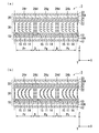
図1(a)は、第1実施形態の液晶装置1の画素を拡大して示す平面図であり、図1(b)は、図1(a)のB−B線に沿う断面図である。図1(a)に示すように、本実施形態の液晶装置1は、行列状に配置された複数の画素(有効画素領域)Pを有しており、複数の画素Pの間が非有効画素領域Dになっている。本実施形態では、複数の画素Pの各々が略長方形状になっている。
FIG. 1A is an enlarged plan view showing a pixel of the
以下、図1(a)に示したXYZ直交座標系を設定し、これに基づいて部材の位置関係を説明する。このXYZ直交座標系においてX方向及びY方向は、画素Pが配置された面に沿っており、画素Pの短辺方向をX方向、長辺方向をY方向としている。また、画素Pの配置面と直交する方向をZ方向としている。 Hereinafter, the XYZ orthogonal coordinate system shown in FIG. 1A is set, and the positional relationship of the members will be described based on this. In the XYZ orthogonal coordinate system, the X direction and the Y direction are along the plane on which the pixel P is arranged, and the short side direction of the pixel P is the X direction and the long side direction is the Y direction. A direction orthogonal to the arrangement plane of the pixels P is defined as a Z direction.
図1(b)に示すように、液晶装置1は、画素電極(第1電極)11を有する素子基板(第1基板)10、素子基板10と対向配置され共通電極(第2電極)21を有する対向基板20、及びこれら基板間に挟持された液晶層30を備えている。
As shown in FIG. 1B, the
素子基板10は、例えばアクティブマトリクス型のものであり、ガラスや石英、プラスチック等からなる透明基板10Aを基体としている。透明基板10Aの液晶層30側(Z正方向側)には、薄膜トランジスタ(TFT)等のスイッチング素子、データ線や走査線等の各種配線等を有する素子形成層13が設けられている。データ線は画像信号を供給するデータ線駆動回路と電気的に接続されており、走査線は走査信号を供給する走査線駆動回路と電気的に接続されている。スイッチング素子や各種配線を覆って絶縁膜が設けられている。絶縁膜の液晶層30側には画素Pごとに島状の画素電極11が形成されており、画素電極11の各々はスイッチング素子と電気的に接続されている。スイッチング素子は、走査信号に基づいて画像信号をスイッチングし、これを画素電極11に所定のタイミングで供給するようになっている。
The
これらスイッチング素子や各種配線と重なる部分の素子形成層13に遮光部13dが形成されている。Z方向において遮光部13dと重なる領域が非有効画素領域Dとなっており、非有効画素領域Dは遮光部13dにより規定されている。遮光部13の非形成領域が画素Pになっており、照明光が画素Pを通るようになっている。ここでは、画素電極11が画素Pからその周辺の非有効画素領域Dに張出して形成されている。透明基板10Aにおける液晶層30と反対側(Z負方向側)には、偏光板12が設けられている。
A
画素Pにおける画素電極11の液晶層30側には第1配向膜14が設けられており、ここでは画素Pと第1配向膜14の形成領域とがほぼ一致している。非有効画素領域Dにおける第1配向膜14の間、すなわち画素電極11間の透明基板10Aと画素電極11の周縁とを覆って第2配向膜15が設けられている。なお、少なくとも画素Pの全体と重なるように第1配向膜14が配置されていればよく、画素Pから画素P周辺の非有効画素領域Dに張出して第1配向膜14が設けられていてもよい。
The
第1配向膜14の形成材料としては、ポリイミド垂直配向材(例えば、日産化学工業製RN1719)、シリカゾルゲルやアルミナゾルゲルからなる酸化物ゾルゲル垂直配向材、長鎖アルキルシランカップリング剤等が挙げられる。長鎖アルキルシランカップリング剤としては、炭素数が6〜20程度のアルキル基を有するもの、例えばオクタデシルトリエトキシシランやヘキシルジメチルエトキシシラン等が挙げられる。酸化物ゾルゲル垂直配向材や長鎖アルキルシランカップリング剤等の無機成分を含んだ第1配向膜を採用すれば、ここを通る光による光分解や光の吸収による熱分解等に対する化学的安定性が高くなる。第2配向膜15の形成材料としては、公知の水平配向材を用いることができ、その一例としてはポリイミド水平配向材(例えば、日産化学工業製SE3140)が挙げられる。
Examples of the material for forming the
本発明において第1配向膜14及び第2配向膜15は、各々の表面硬さが互いに異なる状態に形成された後、一括してラビング処理されて形成されている。本実施形態では、前記のような材料選択によって、形成材料を焼成した後の第1配向膜14の表面硬さを第2配向膜15よりも高くしており、形成後においても第1配向膜14の表面硬さは第2配向膜15よりも高くなっている。これにより第1配向膜14と第2配向膜15とで、液晶層30の液晶分子を配向させる配向規制力が異なっている。配向規制力が異なって形成されるメカニズムについては、[第4実施形態]で説明する。ここでは、表面硬さの定義としてヤング率、剛性率等の弾性率を用いている。一般に、弾性率が高いものは硬度も高いので、弾性率の代わりにビッカーズ硬さ、ブリネル硬さ、ロックウェル硬さ等の硬度を硬さ定義に用いてもよい。各種定義のうちのいずれか1つに基づいて、第1配向膜14と第2配向膜15との相対的な表面硬さを評価すればよい。
In the present invention, the
本実施形態の液晶層30は、誘電異方性が負の液晶材料からなっている。第1配向膜14は、これとZ正方向に重なる部分の液晶層30において液晶分子を垂直配向させる配向規制力を有している。第2配向膜15は、第1配向膜14よりも液晶分子を水平配向させる配向規制力が強くなっている。本発明において、垂直配向とは液晶分子の極方向が透明基板10Aの法線方向(Z方向)となす角度であるプレチルト角が45°未満である配向状態を意味する。また、本発明はマルチドメインの液晶装置に関するものであり、水平配向とは、垂直配向の液晶層側よりもプレチルト角が大きい配向状態を意味する。ここでは、画素Pにおける液晶分子のプレチルト角を0〜3°程度にしており、非有効画素領域Dにおける液晶分子のプレチルト角を画素P側よりも大きくしている。
The
対向基板20は、ガラスや石英、プラスチック等からなる透明基板20Aを基体としている。透明基板20Aの液晶層30側(Z負方向側)にはベタ状の共通電極21が設けられており、その液晶層30側には第3配向膜22が設けられている。本実施形態の第3配向膜22は、画素Pと非有効画素領域Dとにわたってベタ状に形成されており、画素Pと非有効画素領域Dとで配向規制力が同様になっている。透明基板20Aにおける液晶層30と反対側(Z正方向側)には、偏光板23が設けられている。ここでは、偏光板12と偏光板23とで、各々の光学軸が直交するようになっている。
The
以上のような液晶装置1に、画素電極11に画像信号が供給されていない状態でZ方向の一方(例えば、Z負方向)から照明光が供給されると、非有効画素領域Dでは照明光が遮光部13dによって遮られる。また、画素Pに入射した照明光のうち偏光板12の光学軸に直交する偏光が偏光板12に吸収され、光学軸に沿った偏光が偏光板12を通って液晶層30に入射する。画素Pの液晶層30で液晶分子が垂直配向しているので、ここに入射した光はその偏光状態がほとんど変化することなく対向基板20に入射する。対向基板20に入射した光は、偏光板23の光学軸が偏光板12と略直交しているので、そのほとんどが偏光板23に吸収される。このようにして、高品質な黒表示が得られるようになっている。
When illumination light is supplied from one of the Z directions (for example, the Z negative direction) to the
また、画素電極11に画像信号が供給された状態で照明光が供給されると、画素Pでは偏光板12の光学軸に沿った偏光が液晶層30に入射する。画素電極11と共通電極21との間には画像信号に応じた電界が印加されており、この電界に応じて画素Pにおける液晶分子の方位角が変化する。液晶分子の方位角が変化する向き(液晶分子が倒れる方向)は、非有効画素領域Dの液晶分子が水平配向しているので、この配向性により規制される。これにより、液晶分子が倒れる方向にばらつきを生じることによるディスクリネーションの発生が防止され、ディスクリネーションによるコントラスト低下が防止される。画素Pにおける液晶層30に入射した光は、液晶分子の方位角に応じて偏光状態が変化して対向基板20に入射する。対向基板20に入射した光は、その偏光状態の変化に応じて偏光板23の光学軸に直交する偏光が吸収され、対向基板20から射出される。このように、画像信号に応じた階調の光が得られるようになっている。
When illumination light is supplied in a state where an image signal is supplied to the
なお、第1実施形態では、偏光板12と偏光板23とで光学軸が直交した構成を採用したが、これらの光学軸が互いに平行となる構成としてもよい。この場合には、画像信号が供給されていない状態で、液晶装置に供給された光がほとんど吸収されずに射出されるため、高品質な白表示が得られるようになる。
また、対向基板20の第3配向膜22が、素子基板10側と同様に画素Pにおいて非有効画素領域Dよりも液晶分子を水平配向させる配向規制力が弱くなっている構成としてもよいし、第3配向膜を省いた構成を採用することもできる。非有効画素領域Dにおける対向基板20側に遮光部13dと同様の遮光部材を配置してもよい。
In the first embodiment, the
In addition, the
[第2実施形態]
次に、第1実施形態と異なる構成の液晶装置を説明する。第2実施形態が第1実施形態と異なる点は、直視型のフルカラー液晶表示装置に本発明を適用した点である。
[Second Embodiment]
Next, a liquid crystal device having a configuration different from that of the first embodiment will be described. The second embodiment is different from the first embodiment in that the present invention is applied to a direct-view type full-color liquid crystal display device.
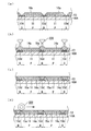
図2(a)は、第2実施形態の液晶装置2の画素を拡大して示す平面図であり、図2(b)は、図2(a)のC−C線に沿う断面図である。図2(a)に示すように、液晶装置2は、行列状に配置された複数のサブ画素(有効画素領域)Pr、Pg、Pbを有しており、サブ画素Pr、Pg、Pbの間が非有効画素領域Dになっている。
2A is an enlarged plan view showing a pixel of the
本実施形態の対向基板20には、透明基板20Aと共通電極21との間にカラーフィルタ層24が設けられている。カラーフィルタ層24には、サブ画素Pr、Pg、Pbの各々に対応した色材部24r、24g、24bが設けられている。色材部24r、24g、24bの間に遮光部24dが設けられており、遮光部24dとZ方向に重なる領域が非有効画素領域Dになっている。すなわち、非有効画素領域Dは遮光部24dによって規定されている。なお、本実施形態の素子基板10には遮光部が設けられていないが、第1実施形態と同様に遮光部が設けられていてもよい。
In the
本実施形態の色材部24r、24g、24bは、それぞれ赤色光、緑色光、青色光に対応している。例えば、色材部24rを通る光は、その赤色光以外の波長帯域光が色材部24rに吸収され、サブ画素Prから赤色光が射出される。このようにして、サブ画素Pr、Pg、Pbからそれぞれ赤色光、緑色光、青色光が射出され、これらが混ざり合って視認されることでフルカラーの1画素が構成される。第2実施形態の液晶装置2にあっても、サブ画素Pr、Pg、Pbの各々における液晶層30にディスクリネーションを生じることが防止され、高品質な画像が得られるようになっている
The
[第3実施形態]
次に、第1、第2実施形態と異なる構成の液晶装置を説明する。第3実施形態が第1、第2実施形態と異なる点は、OCBモードのフルカラー液晶表示装置に本発明を適用した点である。
[Third Embodiment]
Next, a liquid crystal device having a configuration different from the first and second embodiments will be described. The third embodiment is different from the first and second embodiments in that the present invention is applied to an OCB mode full-color liquid crystal display device.
図3(a)、(b)は、第3実施形態の液晶装置3の構成を示す要部断面図である。液晶装置3は、第2実施形態と画素の構成が同様になっており、図3(a)、(b)には、図2(a)のC−C線に沿う断面図に対応する部分を示している。図3(a)には液晶装置3の電源投入時の状態を示しており、図3(b)には液晶装置3の表示動作時の状態を示している。
FIGS. 3A and 3B are cross-sectional views of the main part showing the configuration of the
本実施形態でも第1、第2実施形態と同様に、第1配向膜14及び第2配向膜15は、各々の表面硬さが互いに異なる状態に形成された後、一括してラビング処理されて形成されている。本実施形態では、第1配向膜14の表面硬さが第2配向膜15よりも低くなっており、ラビング処理により付与された配向規制力、すなわち液晶分子を水平配向させる配向規制力が第1配向膜14において第2配向膜15よりも強くなっている。
Also in this embodiment, as in the first and second embodiments, the
第1配向膜14は、例えばポリイミド水平配向材からなり、画素Pの液晶層30において液晶分子を水平配向させる配向規制力を有している。また、第1配向膜14と対向基板20の第3配向膜22とは、いずれも同じ方向(ここではX正方向)に向かってラビング処理されている。これにより、サブ画素Pr、Pg、Pbの各々において液晶分子は、X正方向側に向かって扇状に開いたスプレイ配向になっている。第2配向膜15は、例えばポリイミド垂直配向材からなり、第1配向膜14よりも液晶分子を水平配向させる配向規制力が弱くなっている。これにより、非有効画素領域Dでは、サブ画素Pr、Pg、Pbよりも液晶分子の配向状態が垂直配向に近くなっている。
The
図3(b)に示すように、液晶装置3の表示動作時には、液晶分子が基板間で弓なりに曲がって配向(ベンド配向)するようになっている。ベンド配向は、その曲がり度合いが画素電極11と共通電極21との間の電界に応じて変化する。これにより、サブ画素Pr、Pg、Pbの各々における液晶層30を通る光の偏光状態が画像信号に応じて変化し、画像信号に応じた階調の光が液晶装置3から射出されるようになっている。
As shown in FIG. 3B, during the display operation of the
このようなOCBモードの液晶装置3に表示動作を行わせるためには、電源投入後に液晶層30で液晶分子の配向をスプレイ配向からベンド配向に初期転移する必要がある。通常はこの初期転移において、ディスクリネーション等を核としてスプレイ配向から垂直配向に転移させ、さらに垂直配向からベント配向に転移させている。液晶装置3においては、非有効画素領域Dの液晶分子が、垂直配向あるいは画素Pよりも垂直配向に近い状態に配向しているので、サブ画素Pr、Pg、Pbにおける液晶分子のスプレイ配向から垂直配向への転移が促進され、良好に初期転移を行うことが可能になる。
In order to cause the OCB mode
[第4実施形態]
次に、第1実施形態の液晶装置1の構成に基づいて、本発明に係る液晶装置の製造方法の実施形態を説明する。本発明の液晶装置の製造方法は、素子基板(第1基板)10を形成する工程と、対向基板(第2基板)20を形成する工程と、素子基板10と対向基板20とを貼合せるとともにこれら基板間に液晶層30を封止する工程とを有している。対向基板20を形成する工程と、液晶層30を封止する工程とは、公知の形成材料や公知の形成方法を用いることができる。以下、素子基板10の形成する工程を中心に説明を行う。
[Fourth Embodiment]
Next, an embodiment of a method for manufacturing a liquid crystal device according to the present invention will be described based on the configuration of the
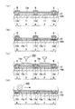
図4(a)〜(d)、図5(a)〜(d)は、第4実施形態の液晶装置の製造方法を概略して示す断面工程図である。
まず、図4(a)に示すように、透明基板10A上に遮光部13dを有する素子形成層13を形成し、素子形成層13上に島状の画素電極11を形成する。具体的には、ガラスや石英、プラスチック等の透光性を有する透明基板10Aに、図示略の走査線、データ線等の各種配線やスイッチング素子等を形成する。こららは、適宜層間絶縁膜等を介して配置し、各種配線やスイッチング素子と重なる部分に遮光部13dを形成しておく。そして、スイッチング素子と電気的に接続された島状の画素電極11を形成する。画素電極11は、画素Pとなる領域からその周辺に張出して形成する。以下、後に画素Pになる領域を単に画素Pと称し、後に非有効画素領域Dとなる領域を単に非有効画素領域Dと称する場合がある。
FIGS. 4A to 4D and FIGS. 5A to 5D are cross-sectional process diagrams schematically showing a method for manufacturing the liquid crystal device of the fourth embodiment.
First, as shown in FIG. 4A, the
次いで、図4(b)に示すように、透明基板10Aと画素電極11とを覆って第1材料膜14aを形成する。第1材料膜14aは後に第1配向膜14となる膜であり、形成材料の選択により第1材料膜14aと後述する第2材料膜15aとで表面硬さを異ならせる。本実施形態では、第1材料膜14aの表面硬さが、第2材料膜15aよりも高くなるようにする。ここでは、ポリイミド垂直配向材(例えば、日産化学工業製RN1719)を形成材料とし、これを塗布法で透明基板10A上と画素電極11上とにベタ状に成膜する。そして、この膜を焼成して後述するポジ型フォトレジストに対して不溶な第1材料膜14aを形成する。
Next, as illustrated in FIG. 4B, a
次いで、図4(c)に示すように、画素Pにおける第1材料膜14aを覆ってレジストパターンRを形成する。ここでは、第1材料膜14aを覆ってポジ型フォトレジスト(例えば、住友化学株式会社製PFM12)をベタ状に成膜し、このフォトレジスト膜を150℃以下の基板温度で焼成する。そして、例えばg線(波長436nm)やi線(波長365nm)を遮光する遮光部を有したフォトマスクを、その遮光部の全体が画素Pの全体に重なるように配置する。そして、フォトマスクを介してフォトレジスト膜にg線やi線を照射してこの膜を露光し、アルカリ現像液等を用いてこの膜を現像することにより、レジストパターンRが得られる。
Next, as illustrated in FIG. 4C, a resist pattern R is formed so as to cover the
なお、前記の基板温度の設定は、以下のような理由に基づいている。本発明者は、後に行うプロセスでレジストパターンRを第1材料膜14aから良好に剥離することが可能な条件について調査した。その結果、一般にフォトレジストには下地(ここでは第1材料膜14a)との密着性を高めるカップリング剤等の成分が含まれており、基板温度を150℃以下にすればこの成分の化学反応が抑制されることが分かった。基板温度を調整することによりレジストパターンRと第1材料膜14aとの密着性を制御することができ、特に基板温度を150℃以下にすれば第1材料膜14aに表面荒れを生じることなくレジストパターンRを剥離することができる。
The setting of the substrate temperature is based on the following reason. The present inventor investigated the conditions under which the resist pattern R can be satisfactorily peeled from the
次いで、図4(d)に示すように、レジストパターンRをマスクとし、エッチング等により非有効画素領域Dの第1材料膜14aを除去してこれをパターニングする。エッチングにはドライエッチング法、ウエットエッチング法のいずれを用いてもよい。例えば、酸素プラズマによるアッシングをドライエッチング法として用いれば、パターニングが容易になる。
Next, as shown in FIG. 4D, using the resist pattern R as a mask, the
次いで、図5(a)に示すようにレジストパターンRを除去する。150℃以下の基板温度で焼成してレジストパターンRを形成しているので、レジストパターンRを良好に剥離し除去することができる。なお、レジストパターンRを除去せずに次の処理を行うこともでき、この手法については[第5実施形態]で説明する。 Next, the resist pattern R is removed as shown in FIG. Since the resist pattern R is formed by baking at a substrate temperature of 150 ° C. or lower, the resist pattern R can be peeled and removed satisfactorily. The following process can be performed without removing the resist pattern R, and this technique will be described in [Fifth Embodiment].
次いで、図5(b)に示すように、画素電極11及び第1材料膜14aを隔壁として、非有効画素領域Dにおける透明基板10A上に、液滴吐出ヘッド200を用いて第2材料膜15aの液状の形成材料を配置する。第2材料膜15aは、後に第2配向膜15となる膜であり、ここでは液状の形成材料としてポリイミド垂直配向材を含んだ溶液を用いる。
Next, as illustrated in FIG. 5B, the
次いで、図5(c)に示すように、配置された液状体を乾燥・焼成等により固形状にして第2材料膜15aを形成する。ここでは、配置する液状体の体積、すなわち液滴吐出ヘッド200からの吐出量を調整することにより第2材料膜15aの膜厚を制御し、第2材料膜15aの上面と第1材料膜14aと上面の段差高さを0.1μm以下にする。
Next, as shown in FIG. 5C, the arranged liquid material is solidified by drying, baking, or the like to form the
次いで、図5(d)に示すように第1材料膜14aと第2材料膜15aとに一括してラビング処理する。具体的には、第1材料膜14a及び第2材料膜15aが形成された透明基板10Aを処理ステージに着脱可能に固定する。そして、表面にラビング布を配置したラビング用ローラ300を第1材料膜14aの表面や第2材料膜15aの表面に接触させる。そして、接触した状態からさらにラビング用ローラ300を処理ステージ側に所定の
高さ(押し込み量)だけ押し込むことにより、ラビング用ローラ300で第1材料膜14aや第2材料膜15aを押圧する。そして、処理ステージをラビング用ローラ300に対して所定の相対速度で移動させるとともに、ラビング用ローラ300を所定の回転数で回転させる。前記の押し込み量、相対速度、回転数によりラビング強度が規定され、ラビング強度に応じて液晶分子を水平配向させる配向規制力が第1材料膜14a、第2材料膜15aのそれぞれに付与される。
Next, as shown in FIG. 5D, the
配向膜に配向規制力が付与されるメカニズムとしては、以下のようなことが考えられている。ラビング布の繊維によって配向膜表面にラビング強度に応じたずり応力がかかり、この応力と配向膜の表面硬さに応じて配向膜表層がラビング方向に延伸される。この繊維が他の位置に移動すると、延伸された配向膜表層は変形緩和していくが完全に元の状態に回復せず、ラビング方向に沿ったひずみが残留する。この残留ひずみによって配向膜に電気的な偏りや表面形状の偏りが生じ、この偏りによって液晶分子が配向するようになる。配向膜の表面硬さを高くすれば、ずり応力による変形量が小さくなるので配向規制力が弱くなる。 The following is considered as a mechanism for imparting alignment regulating force to the alignment film. A shear stress corresponding to the rubbing strength is applied to the surface of the alignment film by the fibers of the rubbing cloth, and the alignment film surface layer is stretched in the rubbing direction according to the stress and the surface hardness of the alignment film. When this fiber moves to another position, the stretched alignment film surface layer is deformed and relaxed, but is not completely restored to the original state, and strain along the rubbing direction remains. This residual strain causes an electrical bias and a surface shape bias in the alignment film, and the liquid crystal molecules are aligned by this bias. If the surface hardness of the alignment film is increased, the amount of deformation due to shear stress is reduced, so that the alignment regulating force is weakened.
ラビング強度としては、以下のような方法により定めればよい。
1つの方法は、第1配向膜14に所望の配向規制力を付与するラビング強度とする方法である。第1材料膜14aの表面硬さが第2材料膜15aよりも高い場合には、第2材料膜15aに対してラビング強度が過剰になり、ここにキズやスジ等を生じることがある。しかしながら、第2配向膜15は非有効画素領域Dに設けられるので、キズ等が視認されないので画像の品質が低下することがない。また、第2配向膜15にキズ等を生じていてもその配向規制力はほとんど低下しないので、液晶分子を水平配向させる配向規制力を有する第2配向膜15となり、画素Pの液晶分子の配向方向を規制する機能が損なわれることもない。
The rubbing strength may be determined by the following method.
One method is a method of setting the rubbing strength to give a desired alignment regulating force to the
もう1つの方法は、第2配向膜15に所望の配向規制力を付与するラビング強度とする方法である。画素Pの液晶分子を透明基板10A、20Aに対して垂直配向させる場合には、液晶分子のプレチルト角を小さくする側に大きなマージンがある。すなわち、プレチルト角が0°より大きくなっていれば液晶分子の倒れる方向が揃いやすくなる効果が得られるため、第1配向膜14において液晶分子を水平配向させる配向規制力を強くする必要がない。そのため、第2材料膜15aに適したラビング強度でラビング処理すれば第1材料膜14aに多少なりとも配向規制力を付与することができ、第1配向膜14と第2配向膜15とがともに良好に機能する程度に配向規制力が付与される。
The other method is a method of setting the rubbing strength to give a desired alignment regulating force to the
このようしてラビング処理することにより、良好な第1配向膜14及び第2配向膜15が得られる。そして、透明基板10Aにおいて画素電極11と反対側に、図1(b)に示した偏光板12を形成すること等により、素子基板10が得られる。また、素子基板10と独立してあるいは一部のプロセスを共通させて対向基板20を形成する。そして、素子基板10と対向基板20とを、画素電極11側と共通電極21側とを内側にして対向配置し、これら基板間に液晶層30を封止すること等により液晶装置1が得られる。
By performing the rubbing process in this way, a good
以上のような本発明の液晶装置の製造方法にあっては、表面硬さが互いに異なる第1材料膜14aと第2材料膜15aとを形成した後に、第1材料膜14aと第2材料膜15aとに一括してラビング処理しているので、配向規制力が互いに異なる第1配向膜14と第2配向膜15とを効率よく形成することができる。ラビング条件を異ならせて複数回数のラビング処理を行う必要がないので、良好な液晶装置を低コストで製造することが可能になる。
In the manufacturing method of the liquid crystal device of the present invention as described above, after forming the
これにより得られた本発明の液晶装置にあっては、第1配向膜14と第2配向膜15とで配向規制力が異なるので、画素Pと非有効画素領域Dとで液晶層30の液晶分子が異なる配向状態となる。したがって、非有効画素領域Dの液晶分子の配向性により画素Pの液晶分子の配向性を制御することが可能になり、高品質な画像が得られる液晶装置となる。また、効率よく製造することが可能になっているので、低コスト化が可能な液晶装置となる。
In the liquid crystal device of the present invention thus obtained, since the alignment regulating force differs between the
なお、第1実施形態の液晶装置1に基づいて説明したが、同様にして第2実施形態の液晶装置2を製造することもできる。また、第1配向膜の形成材料として前記の水平配向材を用いるとともに、第2配向膜材料として前記の垂直配向材を用いることにより、第3実施形態の液晶装置3を製造することもできる。
また、第4実施形態では、レジストパターンRをマスクにして第1材料膜14aをパターニングしたが、光感光性の樹脂、例えば紫外線感光型のポジ型ポリイミド樹脂等を成膜して第1材料膜14aとし、これを露光・現像によりパターニングしてもよい。露光・現像によりパターニングすれば、プロセスが簡略化される。一方、第4実施形態のようにレジストパターンRを用いてパターニングすれば、第1配向膜14の位置精度が高くなり、これに伴って第2配向膜15の位置精度も高くなる。
In addition, although demonstrated based on the
In the fourth embodiment, the
[第5実施形態]
次に、前記第4実施形態と異なる態様の液晶装置の製造方法を説明する。本実施形態が第4実施形態と異なる点は、第1材料膜よりも第2材料膜を先に形成する点と、レジストパターンを隔壁に用いて、液状の形成材料を配置する点である。
[Fifth Embodiment]
Next, a method for manufacturing a liquid crystal device having a mode different from that of the fourth embodiment will be described. This embodiment is different from the fourth embodiment in that the second material film is formed before the first material film, and that a liquid forming material is arranged using a resist pattern as a partition wall.
図6(a)〜(d)は、第5実施形態の液晶装置の製造方法を概略して示す断面工程図である。
まず、図6(a)に示すように、透明基板10A上に遮光部13dを有する素子形成層13や画素電極11を形成し、透明基板10Aと画素電極11とを覆ってベタ状の第2材料膜15aを形成した後、非有効画素領域Dにおける第2材料膜15a上にレジストパターンRを形成する。これらは、第4実施形態と同様の形成方法や形成材料を用いて形成することができる。
6A to 6D are cross-sectional process diagrams schematically showing a method for manufacturing the liquid crystal device of the fifth embodiment.
First, as shown in FIG. 6A, the
次いで、図6(b)に示すように、レジストパターンRをマスクにして画素Pの第2材料膜15aを除去しこれをパターニングする。本実施形態では、パターニング後にレジストパターンRを第2材料膜15aから剥離せずに保持しておく。
次いで、図6(c)に示すように、画素電極11上面とレジストパターンRとの段差部分を隔壁にして、画素Pにおける画素電極11上に第1材料膜14aの液状の形成材料を液滴吐出ヘッド200により配置する。レジストパターンRの膜厚だけ隔壁内側の容積が大きくなるので、ここに配置する液状の形成材料の量を調整することが容易になり、第1材料膜14aの膜厚制御が容易になる。また、隔壁の内側から液状の形成材料が溢れにくくなるので、液状の形成材料を配置する位置精度が高くなる。
Next, as shown in FIG. 6B, the
Next, as shown in FIG. 6C, a liquid material for forming the
そして、配置された液状体を乾燥・焼成することにより第1材料膜14aを形成する。150℃以下の基板温度で焼成することにより、第2材料膜15aとレジストパターンRとの化学反応を抑制することができる。そして、第4実施形態と同様にして第2材料膜15aからレジストパターンRを剥離し、適宜リンス処理等を行う。150℃以下の基板温度で焼成して第1材料膜14aを形成しているので、レジストパターンRを良好に剥離することができる。また、非加熱で乾燥させた場合に比べて、第1材料膜14aと下地(ここでは画素電極11)との密着性が強くなり、リンス処理等により第1材料膜14aが剥離することが防止される。
And the 1st material film |
次いで、図6(d)に示すように、前記第4実施形態と同様に第1材料膜14aと第2材料膜15aとを一括してラビング処理し第1配向膜14及び第2配向膜15を形成した後、後の工程を行うことにより液晶装置1が得られる。なお、本実施形態も第1実施形態の液晶装置1に基づいて説明したが、第4実施形態と同様に第2実施形態や第3実施形態に適用することも可能である。
Next, as shown in FIG. 6 (d), the
[第6実施形態]
次いで、第4、第5実施形態と異なる態様の液晶装置の製造方法を説明する。本実施形態が第4実施形態と異なる点は、第1材料膜よりも第2材料膜を先に形成した後に、CVD法で第1材料膜を形成する点である。
[Sixth Embodiment]
Next, a method for manufacturing a liquid crystal device having a different aspect from the fourth and fifth embodiments will be described. The present embodiment is different from the fourth embodiment in that the first material film is formed by the CVD method after the second material film is formed before the first material film.
図7(a)〜(c)は、第6実施形態の液晶装置の製造方法を概略して示す断面工程図である。
まず、図7(a)に示すように第5実施形態と同様にして、透明基板10A上に素子形成層13、画素電極11、第2材料膜15aを形成する。そして、第2材料膜15aのパターニング後にレジストパターンRを除去する。
7A to 7C are cross-sectional process diagrams schematically showing a method for manufacturing the liquid crystal device of the sixth embodiment.
First, as shown in FIG. 7A, as in the fifth embodiment, the
次いで、図7(b)に示すように、画素Pにおける画素電極11上にCVD法を用いて第1材料膜14aを形成する。具体的には、第1材料膜14aの形成材料420が入った容器410と、第2材料膜15aが形成された透明基板10Aとを密閉容器400内に放置する。ここでは、第1材料膜14aの形成材料420として炭素数が6〜20程度の長鎖アルキル基を有するシランカップリング剤を用いる。また、容器410を例えば150℃以上の温度で1時間程度加熱することによって、シランカップリング剤の蒸気を画素電極11の表面に接触させる。シランカップリング剤は無機系の反応基を有しているので、有機材料からなる第2材料膜15aと結合せずに、無機材料からなる画素電極11と選択的に結合する。
Next, as illustrated in FIG. 7B, a
次いで、図7(c)に示すように、前記第4実施形態と同様に第1材料膜14aと第2材料膜15aとを一括してラビング処理し第1配向膜14及び第2配向膜15を形成した後、後の工程を行うことにより液晶装置1が得られる。
なお、本実施形態も第1実施形態の液晶装置1に基づいて説明したが、第1配向膜の形成材料にシランカップリング剤を用いることにより、第2実施形態や第3実施形態に適用することも可能である。
Next, as shown in FIG. 7C, the
In addition, although this embodiment was also demonstrated based on the
[電子機器]
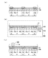
図8は、本発明の電子機器の一実施形態であるプロジェクタ500の概略構成を示す模式図である。図8に示すように、プロジェクタ500は、照明装置510、光変調手段(液晶ライトバルブ)550r、550g、550b、色合成手段(ダイクロイックプリズム)560、投射手段(投射レンズ)570等を備えている。
[Electronics]
FIG. 8 is a schematic diagram showing a schematic configuration of a
照明装置510は、高圧水銀ランプやメタルハライドランプ等の白色ランプ511と、白色ランプ511の光を反射させて前方に射出するリフレクタ512とから構成されている。照明装置510から射出された光は、フライアイレンズアレイ520、偏光変換素子530、色分離手段540を介して液晶ライトバルブ550r、550g、550bに供給される。
The illuminating
フライアイレンズアレイ520は、照明装置510から射出された光の光強度の分布を均一化するものである。これにより、被照明領域である液晶ライトバルブ550r、550g、550bにおいて照度分布が均一化される。
偏光変換素子530は、偏光ビームスプリッタアレイ、1/2波長板アレイ等からなり、照明光の光量を損なうことなく光源光の偏光方向を一方向に揃えるようになっている。
The fly-
The
色分離手段540は、ダイクロイックミラー541a、541b、反射ミラー542a〜542c、平行化レンズ543a〜543e等からなっている。ダイクロイックミラー541a、541bは、所定の波長帯域の色光が選択的に反射し、それ以外の波長帯域の色光が透過するようになっている。例えば、照明装置510から射出された照明光のうち、赤色光Lrがダイクロイックミラー541aを透過するとともに、緑色光Lg及び青色光Lbがダイクロイックミラー541aで反射する。また、ダイクロイックミラー541aで反射した緑色光Lg及び青色光Lbのうち、青色光Lbがダイクロイックミラー541bを透過し、緑色光Lgがダイクロイックミラー541bで反射する。
The color separation means 540 includes
ダイクロイックミラー541aを透過した赤色光Lrは、反射ミラー542aで反射し平行化レンズ543aを経て赤色光用の液晶ライトバルブ550rに入射する。ダイクロイックミラー541aで反射した緑色光Lgは、平行化レンズ543bを経て緑色光用の液晶ライトバルブ550gに入射する。ダイクロイックミラー541bを透過した青色光Lbは、平行化レンズ543c、反射ミラー542b、平行化レンズ543d、反射ミラー542c、平行化レンズ543eを経て青色光用の液晶ライトバルブ550bに入射する。
The red light Lr that has passed through the
液晶ライトバルブ550r、550g、550bは、いずれも本発明の液晶装置で構成されている。液晶ライトバルブ550r、550g、550bの各々は、画像信号に基づいて光を変調して射出するようになっている。液晶ライトバルブ550r、550g、550bで変調された赤色光Lr、緑色光Lg、青色光Lbは、クロスダイクロイックプリズム560に入射するようになっている。
The liquid
クロスダイクロイックプリズム560は、三角柱プリズムが貼り合わされた構造となっており、その内面に赤色光Lrが反射し緑色光Lgが透過するミラー面と、青色光Lbが反射し緑色光Lgが透過するミラー面とが互いに直交して形成されている。赤色光Lr、緑色光Lg、青色光Lbは、これらのミラー面で選択的に反射あるいは透過して同じ側に射出される。これにより、3つの色光が重ね合わされて合成光となる。この合成光は投射レンズ570によってスクリーン580に拡大投射されるようになっている。
以上のようなプロジェクタ500にあっては、光変調手段(液晶ライトバルブ)550r、550g、550bが本発明の液晶装置で構成されているので、高品質な投射画像が得られるとともに低コストなものになっている。
The cross
In the
次に、本発明の液晶装置を光変調手段に用いた表示部を備えた電子機器の実施形態について説明する。 Next, an embodiment of an electronic apparatus provided with a display unit using the liquid crystal device of the present invention as a light modulation means will be described.
図9(a)は、携帯電話の一例を示した斜視図である。携帯電話600は表示部610を備えており、表示部610は本発明の液晶装置により構成されている。
図9(b)は、ワープロ、パソコンなどの携帯型情報処理装置の一例を示した斜視図である。情報処理装置700は、キーボードなどの入力部710、表示部720、筐体730等を備えている。また、表示部720は、本発明の液晶装置により構成されている。
図9(c)は、腕時計型電子機器の一例を示した斜視図である。時計800は表示部810を備えている。表示部810は、本発明の液晶装置により構成されている。
FIG. 9A is a perspective view showing an example of a mobile phone. The
FIG. 9B is a perspective view illustrating an example of a portable information processing apparatus such as a word processor or a personal computer. The
FIG. 9C is a perspective view showing an example of a wristwatch type electronic device. The
図9(a)〜(c)に示す電子機器はいずれも、その表示部が本発明の液晶装置により構成されているので、良好な表示が可能でしかも低コストなものとなっている。 In any of the electronic devices shown in FIGS. 9A to 9C, the display unit is constituted by the liquid crystal device of the present invention, so that good display is possible and the cost is low.
なお、電子機器としては、前記電子機器に限られることなく、種々の電子機器に適用することができる。例えば、ディスクトップ型コンピュータ、マルチメディア対応のパーソナルコンピュータ(PC)及びエンジニアリング・ワークステーション(EWS)、ページャ、ワードプロセッサ、テレビ、ビューファインダ型又はモニタ直視型のビデオテープレコーダ、電子手帳、電子卓上計算機、カーナビゲーション装置、POS端末、タッチパネルを備えた装置等の電子機器に適用することができる。 The electronic device is not limited to the electronic device, and can be applied to various electronic devices. For example, a desktop computer, multimedia personal computer (PC) and engineering workstation (EWS), pager, word processor, television, viewfinder type or monitor direct view type video tape recorder, electronic notebook, electronic desk calculator, The present invention can be applied to an electronic device such as a car navigation device, a POS terminal, or a device provided with a touch panel.
1、2、3・・・液晶装置、10・・・素子基板(第1基板)、11・・・画素電極(第1電極)、14・・・第1配向膜、14a・・・第1材料膜、15・・・第2配向膜、15a・・・第2材料膜、20・・・対向基板(第2基板)、21・・・共通電極(第2電極)、30・・・液晶層、P・・・画素(有効画素領域)、D・・・非有効画素領域 1, 2, 3 ... Liquid crystal device, 10 ... Element substrate (first substrate), 11 ... Pixel electrode (first electrode), 14 ... First alignment film, 14a ... First Material film, 15 ... second alignment film, 15a ... second material film, 20 ... counter substrate (second substrate), 21 ... common electrode (second electrode), 30 ... liquid crystal Layer, P ... pixel (effective pixel area), D ... non-effective pixel area
Claims (6)
前記複数の有効画素領域の各々に配置された第1電極を有する第1基板と、
第2電極を有する第2基板と、
前記第1基板と前記第2基板との間に挟持された液晶層と、
前記複数の有効画素領域において前記第1電極と前記液晶層との間に形成された第1配向膜と、
前記非有効画素領域において前記第1配向膜の間に形成された第2配向膜と、を備え、
前記第1配向膜と前記第2配向膜とは、互いの表面硬さが異なる状態に形成された後に一括してラビング処理されたことにより、前記液晶層の液晶分子を配向させる配向規制力が互いに異なって形成されていることを特徴とする液晶装置。 A liquid crystal device having a plurality of effective pixel regions and a non-effective pixel region disposed between the plurality of effective pixel regions,
A first substrate having a first electrode disposed in each of the plurality of effective pixel regions;
A second substrate having a second electrode;
A liquid crystal layer sandwiched between the first substrate and the second substrate;
A first alignment film formed between the first electrode and the liquid crystal layer in the plurality of effective pixel regions;
A second alignment film formed between the first alignment films in the non-effective pixel region,
The first alignment film and the second alignment film are rubbed together after being formed in a state in which the surface hardness of the first alignment film and the second alignment film are different from each other, so that the alignment regulating force for aligning the liquid crystal molecules of the liquid crystal layer is increased. A liquid crystal device characterized by being formed differently from each other.
前記複数の有効画素領域の各々に配置された第1電極を有する第1基板を形成する工程と、
第2電極を有する第2基板を形成する工程と、
前記第1電極と前記第2電極を内側にして前記第1基板と前記第2基板とを対向配置するとともに、前記第1基板と前記第2基板との間に液晶層を形成する工程と、を有し、
前記第1基板を形成する工程は、
前記複数の有効画素領域の各々において前記第1電極を覆う第1材料膜を形成するとともに、前記非有効画素領域において前記第1材料膜の間に前記第1材料膜と表面硬さが異なる第2材料膜を形成する材料膜形成処理と、
前記第1材料膜と前記第2材料膜とに一括してラビング処理して、前記第1材料膜に前記液晶層の液晶分子を配向させる配向規制力を付与して第1配向膜を形成するとともに、前記第2材料膜に前記第1配向膜と異なる配向規制力を付与して第2配向膜を形成する配向処理と、を含んでいることを特徴とする液晶装置の製造方法。 A method of manufacturing a liquid crystal device having a plurality of effective pixel regions and a non-effective pixel region disposed between the plurality of effective pixel regions,
Forming a first substrate having a first electrode disposed in each of the plurality of effective pixel regions;
Forming a second substrate having a second electrode;
Forming the liquid crystal layer between the first substrate and the second substrate, with the first substrate and the second substrate facing each other with the first electrode and the second electrode inside, and Have
The step of forming the first substrate includes:
A first material film that covers the first electrode is formed in each of the plurality of effective pixel regions, and the surface hardness of the first material film is different between the first material films in the non-effective pixel region. A material film forming process for forming two material films;
The first material film and the second material film are collectively rubbed, and an alignment regulating force for aligning liquid crystal molecules of the liquid crystal layer is applied to the first material film to form a first alignment film. And an alignment treatment for forming a second alignment film by applying an alignment regulating force different from that of the first alignment film to the second material film.
Priority Applications (1)
| Application Number | Priority Date | Filing Date | Title |
|---|---|---|---|
| JP2008129602A JP2009276675A (en) | 2008-05-16 | 2008-05-16 | Liquid crystal device, method of manufacturing liquid crystal device and electronic device |
Applications Claiming Priority (1)
| Application Number | Priority Date | Filing Date | Title |
|---|---|---|---|
| JP2008129602A JP2009276675A (en) | 2008-05-16 | 2008-05-16 | Liquid crystal device, method of manufacturing liquid crystal device and electronic device |
Publications (2)
| Publication Number | Publication Date |
|---|---|
| JP2009276675A true JP2009276675A (en) | 2009-11-26 |
| JP2009276675A5 JP2009276675A5 (en) | 2011-05-19 |
Family
ID=41442153
Family Applications (1)
| Application Number | Title | Priority Date | Filing Date |
|---|---|---|---|
| JP2008129602A Withdrawn JP2009276675A (en) | 2008-05-16 | 2008-05-16 | Liquid crystal device, method of manufacturing liquid crystal device and electronic device |
Country Status (1)
| Country | Link |
|---|---|
| JP (1) | JP2009276675A (en) |
Cited By (3)
| Publication number | Priority date | Publication date | Assignee | Title |
|---|---|---|---|---|
| US9588367B2 (en) | 2014-05-28 | 2017-03-07 | Samsung Display Co., Ltd. | Liquid crystal display and method of manufacturing the same |
| JP2019120930A (en) * | 2018-01-05 | 2019-07-22 | Jnc株式会社 | Alignment substrate with electrode and liquid crystal display element |
| JP2020109441A (en) * | 2019-01-04 | 2020-07-16 | 凸版印刷株式会社 | Dimming device and dimming sheet |
-
2008
- 2008-05-16 JP JP2008129602A patent/JP2009276675A/en not_active Withdrawn
Cited By (6)
| Publication number | Priority date | Publication date | Assignee | Title |
|---|---|---|---|---|
| US9588367B2 (en) | 2014-05-28 | 2017-03-07 | Samsung Display Co., Ltd. | Liquid crystal display and method of manufacturing the same |
| JP2019120930A (en) * | 2018-01-05 | 2019-07-22 | Jnc株式会社 | Alignment substrate with electrode and liquid crystal display element |
| JP7135799B2 (en) | 2018-01-05 | 2022-09-13 | Jnc株式会社 | Oriented substrate with electrodes and liquid crystal display element |
| TWI790293B (en) * | 2018-01-05 | 2023-01-21 | 日商捷恩智股份有限公司 | Oriented substrates with electrodes and liquid crystal display elements |
| JP2020109441A (en) * | 2019-01-04 | 2020-07-16 | 凸版印刷株式会社 | Dimming device and dimming sheet |
| JP7275580B2 (en) | 2019-01-04 | 2023-05-18 | 凸版印刷株式会社 | Light control device and light control sheet |
Similar Documents
| Publication | Publication Date | Title |
|---|---|---|
| JP4858460B2 (en) | Liquid crystal device and manufacturing method thereof | |
| JP4900072B2 (en) | Liquid crystal device and electronic device | |
| JP2009133948A (en) | Liquid crystal device, method for producing the liquid crystal device, and electronic apparatus | |
| US11422418B2 (en) | Liquid crystal device and electronic apparatus | |
| JP2004226829A (en) | Liquid crystal display, its manufacturing method, and electronic device | |
| JP4765962B2 (en) | Manufacturing method of liquid crystal device | |
| JP3835422B2 (en) | Liquid crystal device and electronic device | |
| JP4605110B2 (en) | Liquid crystal device and image display device including the same | |
| JP2009276675A (en) | Liquid crystal device, method of manufacturing liquid crystal device and electronic device | |
| JP4900073B2 (en) | Liquid crystal device and electronic device | |
| JP2007187720A (en) | Liquid crystal device and electronic equipment | |
| JP2006267158A (en) | Microlens substrate, manufacturing method thereof, electro-optical device, manufacturing method thereof, and electronic apparatus | |
| JP2009276678A (en) | Liquid crystal device, method of manufacturing liquid crystal device and electronic device | |
| JP2008170589A (en) | Liquid crystal device, manufacturing method of liquid crystal device and electronic device | |
| JP4604988B2 (en) | Manufacturing method of liquid crystal device | |
| JP4802752B2 (en) | Liquid crystal device and electronic device | |
| JP2008009195A (en) | Liquid crystal display element and projection type liquid crystal display device | |
| JP2008015229A (en) | Liquid crystal device and electronic equipment | |
| US20090015733A1 (en) | Retardation Film and Projection Display Apparatus | |
| US11526057B2 (en) | Liquid crystal device comprising a wall portion extending along a third end and a fourth end of a pixel electrode and covered with the pixel electrode | |
| JP2007133443A (en) | Liquid crystal display device | |
| JP2009276676A (en) | Method of manufacturing liquid crystal device | |
| JP2008225033A (en) | Liquid crystal device, manufacturing of liquid crystal device, and electronic apparatus | |
| JP2009075190A (en) | Manufacturing method for liquid crystal device | |
| JP2008216739A (en) | Liquid crystal device manufacturing method |
Legal Events
| Date | Code | Title | Description |
|---|---|---|---|
| A521 | Written amendment |
Free format text: JAPANESE INTERMEDIATE CODE: A523 Effective date: 20110401 |
|
| A621 | Written request for application examination |
Free format text: JAPANESE INTERMEDIATE CODE: A621 Effective date: 20110401 |
|
| A521 | Written amendment |
Free format text: JAPANESE INTERMEDIATE CODE: A821 Effective date: 20110404 |
|
| A761 | Written withdrawal of application |
Free format text: JAPANESE INTERMEDIATE CODE: A761 Effective date: 20111222 |
|
| A521 | Written amendment |
Effective date: 20111226 Free format text: JAPANESE INTERMEDIATE CODE: A821 |