JP2009231842A - Electromechanical switch, and method of forming the same - Google Patents
Electromechanical switch, and method of forming the same Download PDFInfo
- Publication number
- JP2009231842A JP2009231842A JP2009070509A JP2009070509A JP2009231842A JP 2009231842 A JP2009231842 A JP 2009231842A JP 2009070509 A JP2009070509 A JP 2009070509A JP 2009070509 A JP2009070509 A JP 2009070509A JP 2009231842 A JP2009231842 A JP 2009231842A
- Authority
- JP
- Japan
- Prior art keywords
- memory device
- line
- electrode
- storage node
- beam line
- Prior art date
- Legal status (The legal status is an assumption and is not a legal conclusion. Google has not performed a legal analysis and makes no representation as to the accuracy of the status listed.)
- Pending
Links
Images


Classifications
-
- H—ELECTRICITY
- H01—ELECTRIC ELEMENTS
- H01L—SEMICONDUCTOR DEVICES NOT COVERED BY CLASS H10
- H01L28/00—Passive two-terminal components without a potential-jump or surface barrier for integrated circuits; Details thereof; Multistep manufacturing processes therefor
- H01L28/40—Capacitors
-
- H—ELECTRICITY
- H10—SEMICONDUCTOR DEVICES; ELECTRIC SOLID-STATE DEVICES NOT OTHERWISE PROVIDED FOR
- H10B—ELECTRONIC MEMORY DEVICES
- H10B12/00—Dynamic random access memory [DRAM] devices
- H10B12/01—Manufacture or treatment
- H10B12/09—Manufacture or treatment with simultaneous manufacture of the peripheral circuit region and memory cells
Landscapes
- Engineering & Computer Science (AREA)
- Power Engineering (AREA)
- Computer Hardware Design (AREA)
- Microelectronics & Electronic Packaging (AREA)
- Manufacturing & Machinery (AREA)
- Semiconductor Memories (AREA)
- Micromachines (AREA)
Abstract
Description
本発明は、電機機械的スイッチ及びこれの形成方法に関する。より詳しくは、本発明は移動によってストレージノードと接触する電極を有する電気機械的スイッチ及びこれの形成方法に関する。 The present invention relates to an electromechanical switch and a method for forming the same. More particularly, the present invention relates to an electromechanical switch having an electrode that contacts a storage node by movement and a method of forming the same.
DRAMはセル内に保存されたデータを維持させるためのリフレッシュ動作が要求される固体メモリ(solid state memory)である。前記DRAMのメモリセルは1つのMOSトランジスタと1つのコンデンサを含む。前記コンデンサに保存された電荷は漏洩(leakage)によって消失されるために、前記DRAMはコンデンサ内の電荷値を維持させるために周期的に電荷をリフレッシュさせなければならない。前記MOSトランジスタは前記メモリセルにおいてスイッチの役割をする。もしメモリにリード動作をすれば、前記コンデンサにおいての電圧はセンス増幅器によってデータラインで感知される。もし、ライトまたはリフレッシュ動作の際には、前記データラインは入力ラインになる。動作を願う望ましいアドレス(address)で前記DRAMセルのMOSトランジスタがターン・オンされる際、データが入力されて前記アドレスのDRAMセルのコンデンサに電荷が充電されるか或いは放電されることができる。 The DRAM is a solid state memory that requires a refresh operation to maintain data stored in a cell. The memory cell of the DRAM includes one MOS transistor and one capacitor. Since the charge stored in the capacitor is lost due to leakage, the DRAM must be periodically refreshed to maintain the charge value in the capacitor. The MOS transistor serves as a switch in the memory cell. If the memory is read, the voltage across the capacitor is sensed on the data line by the sense amplifier. If a write or refresh operation is performed, the data line becomes an input line. When the MOS transistor of the DRAM cell is turned on at a desired address desired for operation, data is input and the capacitor of the DRAM cell at the address can be charged or discharged.
前記DRAMの集積度を高めるための1つの方法をもって、前記MOSトランジスタのサイズを減少させることができる。しかし、前記MOSトランジスタのサイズを減少させれば短絡またはジャンクション漏洩などの問題を引き起こすことがある。前記DRAMの集積図を高めるための別の方法をもって、前記メモリセルを多層に積層させることができる。しかし、メモリセルに前記MOSトランジスタを使う際、前記MOSトランジスタは半導体基板上に形成されるべきである。よって、前記半導体基板はMOSトランジスタを含むメモリセルの上部アレイ及び下部アレイの間に各々具備されるべきである。このように、各々の半導体基板はメモリセルの複数の層の間に形成されるべきであるため、前記DRAMの厚さが増加される。 The size of the MOS transistor can be reduced by one method for increasing the degree of integration of the DRAM. However, reducing the size of the MOS transistor may cause problems such as a short circuit or junction leakage. The memory cells can be stacked in multiple layers by another method for increasing the integrated view of the DRAM. However, when using the MOS transistor in a memory cell, the MOS transistor should be formed on a semiconductor substrate. Therefore, the semiconductor substrate should be provided between an upper array and a lower array of memory cells including MOS transistors. Thus, since each semiconductor substrate should be formed between multiple layers of memory cells, the thickness of the DRAM is increased.
従って、メモリ素子に使用することができ、性能が向上したスイッチング素子が要求されている。 Therefore, a switching element that can be used for a memory element and has improved performance is required.
従って、本発明の一目的は高性能を有する電気機械的スイッチング素子の提供にある。 Accordingly, an object of the present invention is to provide an electromechanical switching element having high performance.
本発明の別の目的は前述のスイッチング素子の形成方法の提供にある。 Another object of the present invention is to provide a method for forming the aforementioned switching element.
前述の本発明の一目的を達成するために、本発明の実施例によるメモリ素子は、メモリセル内に、電荷を保存するためのストレージノードが具備される。メモリセル内に、第1電極及び第2電極が具備される。前記第1電極は第2部分と電気的に接続される第1部分を含む。前記第1部分は前記第2電極に電圧が印加された際、移動して前記ストレージノードと接続する。 In order to achieve the above-described object of the present invention, a memory device according to an embodiment of the present invention includes a storage node for storing charges in a memory cell. A first electrode and a second electrode are provided in the memory cell. The first electrode includes a first portion that is electrically connected to a second portion. The first portion moves and connects to the storage node when a voltage is applied to the second electrode.
前記ストレージノードから伝達を受ける前記電荷は前記第1部分を通じて前記第2部分の端部と接続された電圧センシング回路へ伝達されることができる。 The charge received from the storage node may be transmitted through the first part to a voltage sensing circuit connected to an end of the second part.
前記第1部分及び第2部分は前記コンタクトプラグを通じて接続されることができる。 The first part and the second part may be connected through the contact plug.
前記第1部分の第1端部は前記ストレージノードに保存された電荷をリードするか或いは前記ストレージノードに電荷を保存するために、第1位置から第2位置へ移動することができる。 The first end of the first portion can move from a first position to a second position to read charge stored in the storage node or to store charge in the storage node.
前記第2電極に電圧が印加される際、前記第1部分の第1端部が前記ストレージノードと接触するために前記第1部分の第1端部は前記第2位置に位置することができる。 When a voltage is applied to the second electrode, the first end of the first portion may be in the second position because the first end of the first portion contacts the storage node. .
前記第1部分の第2端部は前記コンタクトプラグ上に接触されることができる。 The second end of the first portion may be in contact with the contact plug.
前記第1位置及び第2位置の間の第1距離は前記第2電極とこれに対応する前記第1電極の第1部分との間の第2距離と実質的に同一であり得る。 The first distance between the first position and the second position may be substantially the same as the second distance between the second electrode and the corresponding first portion of the first electrode.
これとは別に、前記第1位置及び第2位置の間の第1距離は前記第2電極とこれに対応する前記第1電極の第1部分との間の第2距離よりも短くあり得る。 Alternatively, the first distance between the first position and the second position may be shorter than the second distance between the second electrode and the corresponding first portion of the first electrode.
前記第1部分は第1膜及び第2膜を含むことができ、前記第1膜は前記第2膜と異なる物質からなることができる。 The first portion may include a first film and a second film, and the first film may be made of a different material from the second film.
前記第1部分は第2部分よりも実質的に短いことができる。 The first portion can be substantially shorter than the second portion.
前記第2電極に電圧が印加される際、前記第2電極が活性化されることができる。 When a voltage is applied to the second electrode, the second electrode can be activated.
メモリ素子は基板をさらに含むことができ、前記基板上に第2部分が形成され、前記基板はガラス、半導体、またはプラスチックの内、少なくとも1つからなることができる。 The memory device may further include a substrate, and a second portion is formed on the substrate, and the substrate may be made of at least one of glass, semiconductor, and plastic.
前記ストレージノードはコンデンサを含み、前記コンデンサは第3電極、誘電膜、及び第4電極を含むことができる。 The storage node may include a capacitor, and the capacitor may include a third electrode, a dielectric film, and a fourth electrode.
前記第3電極は前記第1部分の第1端部を受け入れ、前記第4電極は前記導電性プレート上に形成されることができる。 The third electrode may receive a first end of the first portion, and the fourth electrode may be formed on the conductive plate.
前記ストレージノードは絶縁物質によって囲まれている導電性パターンを含むことができる。 The storage node may include a conductive pattern surrounded by an insulating material.
前記メモリ素子は導電性プレートがさらに含まれることができ、前記導電性プレート上に前記ストレージノードが形成されることができる。 The memory device may further include a conductive plate, and the storage node may be formed on the conductive plate.
前記第1電極はビットラインを含み、前記第2電極はワードラインを含むことができる。 The first electrode may include a bit line, and the second electrode may include a word line.
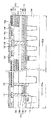
本発明の目的を達成するため、本発明の実施例による集積回路メモリ素子は第1ワードライン及び第1電荷及び第1電荷を保存するための第1ストレージノードを含む第1メモリセルを含む。第2ワードライン及び第2電荷を保存するための第2ストレージノードを含む第2メモリセルを含む。前記第1メモリセルに形成された第1部分と前記第2メモリセルに形成された第2部分を有するビットラインが具備される。前記第1メモリセルに形成された第1部分と前記第2メモリセルに形成された第2部分を有し、前記ビットラインと電気的に接続されるビームラインを含む。前記第1ワードラインに電圧が印加された際、前記ビームラインの第1部分の端部は前記第1ストレージノードと接続されるように移動し、前記第2ワードラインに電圧が印加された際、前記ビームラインの第2部分の端部は前記第2ストレージノードと接続するように移動する。 To achieve the objects of the present invention, an integrated circuit memory device according to an embodiment of the present invention includes a first memory cell including a first word line and a first storage node for storing the first charge and the first charge. A second memory cell including a second word line and a second storage node for storing a second charge is included. A bit line having a first portion formed in the first memory cell and a second portion formed in the second memory cell is provided. A beam line includes a first portion formed in the first memory cell and a second portion formed in the second memory cell, and is electrically connected to the bit line. When a voltage is applied to the first word line, the end of the first portion of the beam line moves to be connected to the first storage node, and when a voltage is applied to the second word line. The end of the second part of the beam line moves to connect to the second storage node.
前記ビットライン及びビームラインはコンタクトプラグを通じて接続されることができる。 The bit line and the beam line may be connected through a contact plug.
前記ビームラインの中心部位は前記コンタクトプラグの上部面と接触されることができる。 A central portion of the beam line may be in contact with an upper surface of the contact plug.
前記ビームラインは前記コンタクトプラグに対して実質的に対称な形状を有することができる。 The beam line may have a substantially symmetric shape with respect to the contact plug.
前記第1ストレージノードから伝達を受けた第1電荷は第1部分を通じて前記第2部分の端部と接続された電圧センシング回路へ伝達されることができる。 The first charge received from the first storage node may be transmitted through the first part to a voltage sensing circuit connected to the end of the second part.
前記ビームラインの第1端部は前記第1ストレージノードに保存された第1電荷をリードするか或いは前記第1ストレージノードに第1電荷を使うために第1位置から第2位置へ移動できる。 The first end of the beam line can move from a first position to a second position to read a first charge stored in the first storage node or to use the first charge in the first storage node.
前記第1ワードラインに電圧が印加された際、前記ビームラインの第1端部が前記第1ストレージノードと接触するために、前記ビームラインの第1端部は前記第2位置に位置できる。 When a voltage is applied to the first word line, the first end of the beam line may be located at the second position because the first end of the beam line contacts the first storage node.
前記第1位置と第2位置との第1距離は前記第1ワードラインとこれに対応する前記ビームライン間の第2距離と実質的に同一であり得る。 A first distance between the first position and the second position may be substantially the same as a second distance between the first word line and the corresponding beam line.
これとは別に、前記第1位置と第2位置間の第1距離は前記第1ワードラインとこれに対応する前記ビームライン間の第2距離よりも短いこともある。 Alternatively, the first distance between the first position and the second position may be shorter than the second distance between the first word line and the corresponding beam line.
前記ビームラインは第1膜及び第2膜を含むことができ、前記第1膜は前記第2膜と異なる物質を含むことができる。 The beam line may include a first film and a second film, and the first film may include a material different from the second film.
前記ビームラインは前記ビットラインよりも実質的に短いことがある。 The beam line may be substantially shorter than the bit line.
前記第1ワードラインは電圧が印加される際、活性化されることができる。 The first word line may be activated when a voltage is applied.
前記メモリ素子は基板をさらに含み、前記基板上に前記ビットラインが形成され、前記基板はガラス、半導体、またはプラスチックの内、少なくとも1つからなることができる。 The memory device may further include a substrate, and the bit line may be formed on the substrate, and the substrate may be made of at least one of glass, semiconductor, and plastic.
前記第1ストレージノードはコンデンサからなることができ、前記コンデンサは第1電極、誘電膜、及び第2電極を含むことができる。 The first storage node may include a capacitor, and the capacitor may include a first electrode, a dielectric film, and a second electrode.
前記第1電極は前記ビームラインの第1端部を受け入れ、前記第2電極は前記導電性プレート上に形成されることができる。 The first electrode may receive a first end of the beam line, and the second electrode may be formed on the conductive plate.
前記第1ストレージノードは絶縁物質によって囲まれている導電性パターンを含むことができる。 The first storage node may include a conductive pattern surrounded by an insulating material.
前記メモリ素子は導電性プレートがさらに含まれることができ、前記導電性プレート上に前記第1ストレージノードが形成されることができる。 The memory device may further include a conductive plate, and the first storage node may be formed on the conductive plate.
本発明の一目的を達成するために、本発明の実施例によるメモリ素子は、ビットラインと接続され、第1ビームラインを有する一対の第1メモリセルを含む。前記一対の第1メモリセルと隣接して形成されて前記ビットラインと接続され、第2ビームラインを有する別の一対の第2メモリセルを含む。各々のワードラインに電圧が印加される際、前記ビームラインは電荷が保存される各々のストレージノードに接続されるように移動することができる。 To achieve one object of the present invention, a memory device according to an embodiment of the present invention includes a pair of first memory cells connected to a bit line and having a first beam line. Another pair of second memory cells formed adjacent to the pair of first memory cells and connected to the bit line and having a second beam line are included. When a voltage is applied to each word line, the beam line can move to be connected to each storage node where charge is stored.
前記ビットライン及び各々のビームラインは各々のコンタクトプラグを通じて電気的に接続されることができる。 The bit line and each beam line may be electrically connected through each contact plug.
前記各々のビームラインは各々のコンタクトプラグ上に接触されることができる。 Each beam line may be contacted on each contact plug.
前記各々のビームラインは前記各々のコンタクトプラグに対して実質的に対称されることができる。 Each beam line may be substantially symmetric with respect to each contact plug.
前記各々のストレージノードから伝達を受けた電荷は前記ビットラインの端部に接続された電圧センシング回路を通じて伝達を受けることができる。 The charge received from each storage node can be transmitted through a voltage sensing circuit connected to the end of the bit line.
前記各々のストレージノードに保存された電荷をリードするか或いは各々のストレージノードに電荷を保存するために、前記各々のビームラインの端部は第1位置から第2位置へ移動できる。 In order to read the charge stored in each storage node or store the charge in each storage node, the end of each beam line can be moved from a first position to a second position.
前記各々のワードラインに電圧が印加された際、前記各々のビームラインの端部は前記ストレージノードと接触されるため、前記各々のビームラインの端部は前記第2位置に位置できる。 When a voltage is applied to each word line, the end of each beam line is in contact with the storage node, so that the end of each beam line can be located at the second position.
前記第1位置と第2位置間の第1距離は前記各々のワードラインとこれに対応する各々のビームライン間の第2距離と実質的に同一であり得る。 The first distance between the first position and the second position may be substantially the same as the second distance between the respective word lines and the corresponding beam lines.
前記第1位置と第2位置間の第1距離は前記各々のワードラインとこれに対応する各々のビームライン間の第2距離よりも短いことがある。 The first distance between the first position and the second position may be shorter than the second distance between the respective word lines and the corresponding beam lines.
前記各々のビームラインは第1膜及び第2膜を含み、前記第1膜は前記第2膜と互いに異なる物質からなることができる。 Each beam line may include a first film and a second film, and the first film may be made of a material different from the second film.
前記各々のビームラインは前記ビットラインよりも実質的に短いことがある。 Each of the beam lines may be substantially shorter than the bit line.
前記各々のワードラインは電圧が印加された際、活性化されることができる。 Each of the word lines can be activated when a voltage is applied.
前記メモリ素子は基板をさらに含み、前記基板上に前記ビットラインが形成され、前記基板はガラス、半導体、またはプラスチックの内、少なくとも1つからなることができる。 The memory device may further include a substrate, and the bit line may be formed on the substrate, and the substrate may be made of at least one of glass, semiconductor, and plastic.
前記各々のストレージノードはコンデンサからなり、前記コンデンサは第1電極、誘電膜、及び第2電極を含むことができる。 Each of the storage nodes may include a capacitor, and the capacitor may include a first electrode, a dielectric film, and a second electrode.
前記第1電極は前記ビームラインの第1端部を受け入れ、前記第2電極は前記導電性プレート上に形成されることができる。 The first electrode may receive a first end of the beam line, and the second electrode may be formed on the conductive plate.
前記各々のストレージノードは絶縁物質によって囲まれている導電性パターンを含むことができる。 Each storage node may include a conductive pattern surrounded by an insulating material.
前記半導体素子は導電性プレートをさらに含み、前記導電性プレート上に前記各々のストレージノードが形成されることができる。 The semiconductor device may further include a conductive plate, and the respective storage nodes may be formed on the conductive plate.
本発明の一目的を達成するために、本発明の実施例によるメモリ素子は、基板及び前記基板上に形成されたビットラインを含む。前記ビットライン上にはワードラインが具備される。前記ワードライン上にはビームラインが具備される。前記ビームラインと基板との間には電荷を保存するためのコンデンサが具備される。前記ビームラインは前記ワードラインに電圧が印加される際、前記コンデンサと接触するように移動できる。 To achieve one object of the present invention, a memory device according to an embodiment of the present invention includes a substrate and a bit line formed on the substrate. A word line is provided on the bit line. A beam line is provided on the word line. A capacitor for storing charges is provided between the beam line and the substrate. The beam line can move to contact the capacitor when a voltage is applied to the word line.
前記メモリ素子は前記ビットライン及びビームラインと接続されるコンタクトプラグをさらに含むことができる。 The memory device may further include a contact plug connected to the bit line and the beam line.
前記メモリ素子は前記ビームライン上に複数の細孔を有する第1層間絶縁膜がさらに含まれることができる。 The memory device may further include a first interlayer insulating layer having a plurality of pores on the beam line.
前記メモリ素子は前記第1層間絶縁膜上に第2層間絶縁膜がさらに含まれることができる。 The memory device may further include a second interlayer insulating layer on the first interlayer insulating layer.
前記コンデンサに保存された電荷をリードするか或いは前記コンデンサに電荷を保存するために、前記ビームラインの第1端部は第1位置から第2位置へ移動できる。 The first end of the beam line can be moved from a first position to a second position in order to read the charge stored in the capacitor or to store the charge in the capacitor.
前記ワードラインに電圧が印加された際、前記ビームラインの第1端部が前記コンデンサと接触されるため、前記ビームラインの第1端部は第2位置に位置できる。 When a voltage is applied to the word line, the first end of the beam line is in contact with the capacitor, so that the first end of the beam line can be located at a second position.
前記ビームラインの第2端部は前記コンタクトプラグと接触される。 The second end of the beam line is in contact with the contact plug.
前記第1部分と第2部分間の第1距離は前記第1ワードラインとこれに対応する前記ビームライン間の第2距離と実質的に同一であることができる。 The first distance between the first part and the second part may be substantially the same as the second distance between the first word line and the corresponding beam line.
前記第1部分と第2部分間の第1距離は前記第1ワードラインとこれに対応する前記ビームライン間の第2距離よりも短いことがある。 The first distance between the first portion and the second portion may be shorter than the second distance between the first word line and the corresponding beam line.
前記ビームラインは第1膜及び第2膜を含むことができ、前記第1膜は第2膜と互いに異なる物質からなることができる。 The beam line may include a first film and a second film, and the first film may be made of a material different from the second film.
前記ビームラインは前記ビットラインよりも実質的に短いことがある。 The beam line may be substantially shorter than the bit line.
前記ワードラインは電圧が印加される際、活性化できる。 The word line can be activated when a voltage is applied.
前記基板は、ガラス、半導体、またはプラスチックの内の少なくとも1つからなることができる。 The substrate may be made of at least one of glass, semiconductor, or plastic.
前記コンデンサは第1電極、誘電膜、及び第2電極を含むことができる。 The capacitor may include a first electrode, a dielectric film, and a second electrode.
前記第1電極は前記ビームラインの第1端部を受け入れ、前記第2電極は前記導電性プレート上に形成されることができる。 The first electrode may receive a first end of the beam line, and the second electrode may be formed on the conductive plate.
前記メモリ素子は導電性プレートがさらに含まれ、前記導電性プレート上に前記コンデンサか形成されることができる。 The memory device may further include a conductive plate, and the capacitor may be formed on the conductive plate.
本発明の一目的を達成するために、本発明の実施例によるメモリ素子の製造方法をもって、基板上に第1セルのビットラインを形成する。前記ビットライン上にワードラインを形成する。前記ワードライン上に第1ギャップを有するビームラインを形成する。前記ビットライン及びビームラインは互いに電気的に接続することができる。前記ビームラインの端部と基板との間にコンデンサを形成する。前記ビームラインの端部は前記コンデンサの上部面と第2ギャップを有する。前記ビーム上に層間絶縁膜を形成する。前記層間絶縁膜上に第2セルのビットラインを形成する。 In order to achieve an object of the present invention, a bit line of a first cell is formed on a substrate using a method of manufacturing a memory device according to an embodiment of the present invention. A word line is formed on the bit line. A beam line having a first gap is formed on the word line. The bit line and the beam line can be electrically connected to each other. A capacitor is formed between the end of the beam line and the substrate. The end of the beam line has a second gap with the top surface of the capacitor. An interlayer insulating film is formed on the beam. A bit line of a second cell is formed on the interlayer insulating film.
前記第1ギャップは実質的に前記第2ギャップと同一である。 The first gap is substantially the same as the second gap.
前記第1ギャップは前記第2ギャップよりも小さい。 The first gap is smaller than the second gap.
本発明の一目的を達成するために、本発明の実施例によるメモリ素子の製造方法をもって、基板上に第1導電膜を形成する。前記基板のペリフェラル領域のトランジスタを形成し、セル領域の基板にビットラインを形成するために、前記導電膜をパターニングする。前記トランジスタとビットライン上に第1層間絶縁膜を形成する。前記セル領域に、前記第1層間絶縁膜上にコンデンサを形成する。前記ペリフェラル領域の第1層間絶縁膜を貫通して第1コンタクトプラグを形成し、前記セル領域の第1層間絶縁膜を貫通して第2コンタクトプラグを形成する。前記第1コンタクトプラグ、第2コンタクトプラグ、及びコンデンサ上に第2導電膜を形成する。前記セル領域にワードラインを形成するために、第2導電膜をパターニングする。前記ワードライン上に第1犠牲膜を形成する。前記第1犠牲膜上にビームラインを形成する。前記ビームライン上に第2犠牲膜を形成する。そして、前記第1及び第2犠牲膜を除去する。 In order to achieve an object of the present invention, a first conductive film is formed on a substrate using a method for manufacturing a memory device according to an embodiment of the present invention. The conductive film is patterned in order to form a transistor in the peripheral region of the substrate and to form a bit line in the substrate in the cell region. A first interlayer insulating layer is formed on the transistor and the bit line. A capacitor is formed on the first interlayer insulating film in the cell region. A first contact plug is formed through the first interlayer insulating film in the peripheral region, and a second contact plug is formed through the first interlayer insulating film in the cell region. A second conductive film is formed on the first contact plug, the second contact plug, and the capacitor. In order to form a word line in the cell region, the second conductive film is patterned. A first sacrificial layer is formed on the word line. A beam line is formed on the first sacrificial layer. A second sacrificial layer is formed on the beam line. Then, the first and second sacrificial films are removed.
前記方法において、前記第2層間絶縁膜上に複数の細孔を有する第2層間絶縁膜を形成する工程をさらに遂行する。 The method further includes the step of forming a second interlayer insulating film having a plurality of pores on the second interlayer insulating film.
前記第1及び第2犠牲膜は前記複数の細孔を通じてエッチングケミカルを流入することによって除去されることができる。 The first and second sacrificial layers may be removed by flowing an etching chemical through the plurality of pores.
前記方法において、前記第2層管絶縁膜上に第3層間絶縁膜を形成する工程をさらに遂行できる。 The method may further include a step of forming a third interlayer insulating film on the second layer tube insulating film.
前記第1犠牲膜は位置別に相互に異なる厚さを有することができる。前記第1犠牲膜は均一な厚さを有することができる。 The first sacrificial layer may have different thicknesses depending on positions. The first sacrificial layer may have a uniform thickness.
以下、添付された図面を参照して本発明の実施例による集積回路メモリセル及びその製造方法に対して詳しく説明するが、本発明が下記の実施例に制限されることはなく、本発明の属する技術の分野における通常の知識を有する者であれば、特許請求の範囲に記載された技術的思想の範疇内において、各種の変更例または修正例に想到し得ることは明らかであり、これらについても、当然に本発明の技術的範囲に属するものと理解される。添付図面において、基板、層(膜)、電極、領域、パッド、パターン、または構造物のサイズは本発明の明確性に基づくために実際より拡大して図示したものである。本発明において、各層(膜)、領域、電極、プラグ、パッド、パターン、または構造物が基板、各層(膜)、領域、電極、プラグ、パッド、またはパターン上の「上に」、「上部に」、または「下部に」形成されることと言及される場合には各層(膜)、領域、電極、プラグ、パッド、パターン、または構造物が直接基板、各層(膜)、領域、パッド、またはパターン上に形成されるか或いは下に位置することを意味するかまたは別の層(膜)、別の領域、別のパッド、別の電極、別のパターン、または別の構造物が基板上に追加的に形成されることができる。また、物質、層(膜)、領域、パッド、電極、パターン、または構造物が「予備」、「第1」、「第2」、及び/または「第3」と言及される場合、このような部材を限定するためではなく、単に各物質、層(膜)、領域、電極、プラグ、パッド、パターン、または構造物を区分するためである。従って、「予備」、「第1」、「第2」、及び/または「第3」は各物質、層(膜)、領域、電極、プラグ、パッド、パターン、または構造物に対して各々選択的にまたは交換的に使われることができる。一方、添付図面全体において、実質的に同一であるか或いは類似の部材に対しては同一の参照符号を使用する。 Hereinafter, an integrated circuit memory cell and a manufacturing method thereof according to embodiments of the present invention will be described in detail with reference to the accompanying drawings. However, the present invention is not limited to the following embodiments, and It is obvious that a person having ordinary knowledge in the technical field to which he belongs can come up with various changes or modifications within the scope of the technical idea described in the claims. Of course, it is understood that it belongs to the technical scope of the present invention. In the accompanying drawings, the size of a substrate, a layer (film), an electrode, a region, a pad, a pattern, or a structure is illustrated on an enlarged scale for the sake of clarity of the present invention. In the present invention, each layer (film), region, electrode, plug, pad, pattern, or structure is “on” or “above” on the substrate, each layer (film), region, electrode, plug, pad, or pattern. ”Or“ underneath ”, each layer (film), region, electrode, plug, pad, pattern, or structure is directly substrate, each layer (film), region, pad, or It means that it is formed on or located below the pattern, or another layer (film), another region, another pad, another electrode, another pattern, or another structure is on the substrate It can additionally be formed. Also, when a substance, layer (film), region, pad, electrode, pattern, or structure is referred to as “spare”, “first”, “second”, and / or “third”, such The purpose is not to limit various members, but to merely distinguish each substance, layer (film), region, electrode, plug, pad, pattern, or structure. Thus, “spare”, “first”, “second”, and / or “third” are selected for each material, layer (film), region, electrode, plug, pad, pattern, or structure, respectively. Can be used automatically or interchangeably. On the other hand, the same reference numerals are used for substantially the same or similar members throughout the drawings.
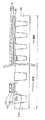
図1は、本発明の一実施例による電気機械的スイッチを示す斜視図である。前記電気機械的スイッチはDRAM素子のようなメモリ素子を構成するメモリセルに使われることができる。前記電気機械的スイッチは前記メモリ素子ではない別の電気素子にも使うことができる。 FIG. 1 is a perspective view showing an electromechanical switch according to an embodiment of the present invention. The electromechanical switch can be used in a memory cell constituting a memory device such as a DRAM device. The electromechanical switch can also be used for another electrical element that is not the memory element.
図1を参照すれば、電気機械的スイッチはメモリセル内に配置される第1電極及び第2電極を含む。前記第1電極はワードライン146であることができ、前記第2電極は空中に浮んでいるビームライン(suspended beam line)160及び埋立ビットライン110を含むビームライン構造であることができる。前記埋立ビットライン110はダイレクトコンタクトを通じて前記ビームライン160と電気的に接続される。前記ダイレクトコンタクトの例としてはコンタクトプラグ136を挙げることができる。前記埋立ビットライン110は基板100上に配置される。前記基板100は、例えば、ガラス、半導体、またはプラスチックを含むことができる。
Referring to FIG. 1, the electromechanical switch includes a first electrode and a second electrode disposed in the memory cell. The first electrode may be a
一実施例として、前記ビームライン160は第1及び第2フレキシブル延長部(160a、160b)を含み、前記第1及び第2フレキシブル延長部(160a、160b)は互いに反対方向へ延長される。前記第1及び第2フレキシブル延長部(160a、160b)は前記コンタクトプラグ136と対応する部位から下方に向かって支持されている。一実施例において、前記ビームライン160及びコンタクトプラグ136の間には導電パターン144が具備されることができる。前記ビームライン160は前記コンタクトプラグ136に対して実質的に対称なように位置できる。前記第1フレキシブル延長部160aの長さは実質的に前記第2フレキシブル延長部160bの長さと同一である。前記ビームライン160の長さは前記埋立ビットライン110の長さより実質的にさらに短い。
As an example, the
一実施例において、前記第1フレキシブル延長部160aの移動は前記第2延長部160bの移動に影響を与えない。例えば、前記第2フレキシブル延長部160bは動かずに前記第1フレキシブル延長部160aは下方に向かって動くことができる。前記第1及び第2フレキシブル延長部(160a、160b)は実質的に曲がっていない形状を有することができる。これとは別の例として、前記第1及び第2フレキシブル延長部(160a、160b)は曲がった形状を有することができる。または前記第1及び第2フレキシブル延長部(160a、160b)は複数の凹んだ部位及び突出された部位を有することができ、前記第1及び第2フレキシブル延長部(160a、160b)の下にはパターンの突出された部位の表面が配置されることができる。
In one embodiment, the movement of the first
一実施例において、前記ビームライン160は第1膜及び第2膜を含む。前記第1膜は第2膜上に積層されることができる。前記第1膜と第2膜は同一の物質を含むことができる。または前記第1膜と第2膜は互いに異なる物質で形成されることができる。例えば、前記第1膜はシリコン酸化膜(SiO2)またはシリコン酸化膜(SiN)を含むことができ、前記第2膜はタンタル(Ta)またはタンタル窒化物(TaN)のようなタンタルを含む導電物質を含むことができる。前記第1及び第2膜が互いに異なる物質からなるビームラインは前記第1及び第2膜が1つの同一物質からなるビームラインと比較する際、さらにフレキシブルである。
In one embodiment, the
前記第1フレキシブル延長部160aと前記埋立ビットライン110の間にはストレージノードが具備される。前記ストレージノードは電荷を保存するための電気的ノードである。前記第1フレキシブル延長部160aとストレージノードが電気的に接続される際、電荷は前記第1フレキシブル延長部160aと前記コンタクトプラグ136を通じて前記埋立ビットライン110の端部と接続されている電圧センシング回路へ移動できる。一実施例において、前記ストレージノードはコンデンサ152の電極ノードであり得る。これとは別の例として、前記ストレージノードは絶縁体によって取り囲まれている電極パターンのノードであり得る。前記コンデンサ152は上部電極130a、下部電極126、及び前記上、下部電極の間に配置される誘電膜128を含む。
A storage node is provided between the first
前記コンデンサ152は前記第1フレキシブル延長部160aの第1端部と隣接するように配置される。前記第1フレキシブル延長部160aの第2端部は前記コンタクトプラグ上に配置される。前記上部電極130aは、例えば、直方体の形状を有することができる。前記第1フレキシブル延長部160aの第1端部は前記上部電極130aと接触されることができる。一実施例として、前記第1フレキシブル延長部160aの第1端部は前記上部電極130aの中心部と接触されることができる。前記第1フレキシブル延長部160aの第1端部と前記上部電極130aが互いに接触する部分はある地点、ライン、または表面になることができる。一実施例として、前記上部電極130a上には導電パッドパターン148がさらに具備されることができる。
The
前記垂直方向に対して調べてみると、前記ワードライン146は前記第1フレキシブル延長部160aと埋立ビットライン110の間の配置されることができる。また、水平方向に対して調べてみると、前記ワードライン146は前記第1フレキシブル延長部160aの第2端部と前記コンデンサ152の間に配置されることができる。前記ワードライン146に電圧が印加された際、前記第1フレキシブル延長部160aの第1端部が下方へ移動することにより前記コンデンサ152と接続される。一実施例において、前記第1フレキシブル延長部160aの第1端部は前記導電パッドパターン148を通じて前記コンデンサ152と電気的に接続されることができる。前記ワードライン146は電圧が印加されることによって活性化されることができる。前記ワードライン146に電圧が印加されることによって前記第1フレキシブル延長部160aに引力が加わる際、前記ワードライン146と前記第1フレキシブル延長部160a間の距離は非常に近くなるが、前記ワードライン146と前記第1フレキシブル延長部160aは互いに接触しないべきである。また、前記第1フレキシブル延長部160aの第1端部は前記コンデンサ152の上部電極130aと接触されるか或いは前記上部電極130a上に形成された導電パッドパターン148と接触されるべきである。データのライト動作において、前記接触によって前記コンデンサ152には電荷が充電されることができる。これと類似にデータのリード動作を遂行する際、前記ワードライン146が前記第1フレキシブル延長部160aに引力を加えることによって前記第1フレキシブル延長部160aの第1端部と上部電極130aまたは前記第1フレキシブル延長部160aの第1端部と上部電極130aの上に形成された導電パッドパターン148が互いに接触するようにする。前記にように接触されれば、前記ビットライン110は前記コンデンサ152内に電荷が存在するかを感知するようになる。
When examined with respect to the vertical direction, the
前記第2フレキシブル延長部160bに対応する第2メモリセルは前記第1フレキシブル延長部160aと対応する第1メモリセルと互いに対称な形状を有する。例えば、ワードライン146が前記第2フレキシブル延長部160bに引力を加える際、前記第2フレキシブル延長部160bは下方へ移動して前記コンデンサ152と接触する。このように、前記ワードライン146に電圧が印加されれば、前記第1フレキシブル160aは移動によって前記コンデンサ152と接触し、前記第2フレキシブル延長部160bと対応する別のワードライン146に電圧が印加されれば、第2フレキシブル延長部160bは移動によって前記第2フレキシブル延長部160bの下に位置する別のコンデンサ152と接続する。
The second memory cell corresponding to the second
前記メモリセルの第1対は前記第1フレキシブル延長部160aを含む第1メモリセルと、前記第2フレキシブル延長部160bを含む第2メモリセルを含む。前記メモリセルの第2対は前記メモリセルの第1対の構造と実質的に同一構造を有し、前記メモリセルの第1対と隣接する部位に形成される。前記メモリセルの第1及び第2対は前記埋立ビットライン110を通じて接続されることができる。このように、規則的な間隔を有して配置される一対以上のメモリセルが前記埋立ビットライン110を通じて互いに接続されることができる。前記ワードライン方向に、互いに対称な延長部を有する一対以上のメモリセルが、例えば、規則的な間隔を有しつつ配置されることができる。
The first pair of memory cells includes a first memory cell including the first
図2は、本発明の一実施例による電気機械的スイッチの移動部分を示す。 FIG. 2 shows the moving part of an electromechanical switch according to an embodiment of the invention.
図2を参照すれば、前記第1フレキシブル延長部161aの第1端部は前記コンデンサ152に保存された電荷をリードするかまたはコンデンサ152に電荷を保存するために第1位置P1から第2位置P2へ移動する。前記ワードライン146に電圧が印加される際、前記第1フレキシブル延長部161aの第1端部は前記コンデンサ152と接触するために前記第2位置P2にあるようになる。一実施例において、前記第1位置P1及び第2位置P2間の第1距離D1は前記ワードライン146とこれに対応して前記ワードライン146の上に位置する前記第1フレキシブル延長部161a間の第2距離D2と実質的に同一である。一実施例において、前記第1距離D1及び第2距離D2は約10nm〜15nmであり得る。
Referring to FIG. 2, the first end of the first
図3は、本発明の一実施例による電気機械的スイッチの移動部分を示す。 FIG. 3 shows the moving part of an electromechanical switch according to an embodiment of the invention.
図3を参照すれば、前記ビームライン162は第1フレキシブル延長部162a及び第2フレキシブル延長部162bを含む。一実施例として第1位置P3と第2位置P4間の第1距離D3は前記ワードライン146とこれに対応して前記ワードライン146上に位置する前記第1フレキシブル延長部162a間の第2距離D4よりさらに短いことがある。一実施例において、前記第1距離D3は約10nm〜15nmであり、前記第2距離D4は約20nm〜25nmであり得る。従って、前記ワードライン146が前記第1フレキシブル延長部162aに引力が加わる際、前記第2距離D4が前記第1距離D3よりさらに長いため、前記第1フレキシブル延長部162aと前記ワードライン146が互いに接触することを防ぐことができる。即ち、前記第1距離D3が0である際にも前記第2距離D4は一定距離で維持できる。前記ワードライン146が前記第1フレキシブル延長部162aと接触すれば、前記ワードライン146及び/または前記第1フレキシブル延長部162aが損傷されて動作不良が発生する。前記メモリ素子の動作電圧は前記第2距離D4が最小距離を維持することができるように下げることができる。
Referring to FIG. 3, the
図4は本発明の一実施例による、ペリフェラル領域に形成されたMOSトランジスタ及びセル領域に形成された電気機械的スイッチを含むメモリ素子を示す断面図である。 FIG. 4 is a cross-sectional view illustrating a memory device including a MOS transistor formed in a peripheral region and an electromechanical switch formed in a cell region according to an embodiment of the present invention.
図4を参照すれば、前記セル領域の基板100にトレンチ素子分離膜102bが具備される。前記基板100は半導体基板であり得る。前記基板100及びトレンチ素子分離膜102b上には埋立ビットライン110が形成される。前記埋立ビットライン110は導電膜パターン104、前記導電膜パターン104上に位置するマスクパターン108を含む。前記埋立ビットライン110上には第1層間絶縁膜114が形成される。前記第1層間絶縁膜114を貫通し、前記埋立ビットライン110の導電膜パターン104と接触するコンタクトプラグ136が具備される。前記コンタクトプラグ136上には導電パッドパターン144が形成されることができる。前記導電パッドパターン144上にはビームライン160が形成されることができる。前記ビームライン160と前記第1層間絶縁膜114上に位置する第2層間絶縁膜134間にはワードライン146が具備される。前記ワードライン146及び第1フレキシブル延長部160a間は第2距離d2ほど離隔されることができる。前記ビームライン160の端部と隣接する部分と第1層間絶縁膜114間にはコンデンサ152が具備される。一実施例において、前記導電パッドパターン148が前記コンデンサ152上に具備されることができる。前記ビームライン160と導電パッドパターン148間は第1距離d1ほど離隔されることができる。前記ワードライン146に電圧が印加されなかった際、前記第1及び第2距離(d1、d2)は実質的に同一である。
Referring to FIG. 4, a
ペリフェラル領域において、前記基板100にはトレンチ素子分離膜102aが形成される。前記基板100上にはゲート電極106及びマスクパターン108を含むMOSトランジスタが形成される。前記ゲート電極106及びマスクパターン108を取り囲むゲートスペーサー116が具備される。前記ゲートスペーサー116に隣接する基板にはソース/ドレイン領域118が形成される。前記ペリフェラル領域のゲート電極106及び前記セル領域の導電性パターン104は同様の膜として形成されることができる。前記層間絶縁膜(114、134)を貫通して前記ソース/ドレイン118と接触するコンタクトプラグ136が具備される。前記コンタクトプラグ136上には導電性ラインパターン150が具備される。
In the peripheral region, a trench
図5は、本発明の一実施例による、ペリフェラル領域及びセル領域を有し、電気機械的スイッチを含むメモリ素子を示す断面図である。 FIG. 5 is a cross-sectional view illustrating a memory device having a peripheral region and a cell region and including an electromechanical switch according to an embodiment of the present invention.
図5を参照すれば、セル領域に、前記図4に図示されたのと類似する構造の電気機械的スイッチが基板300上に形成される。前記基板300はシリコン物質からなっていない基板を使うことができるため、前記基板にトレンチ素子分離膜を省略することができる。前記基板300は、例えば、ガラスまたはプラスチックを含むことができる。ペリフェラル領域に、前記MOSトランジスタに代わって電気機械的スイッチが具備されることができる。
Referring to FIG. 5, an electromechanical switch having a structure similar to that illustrated in FIG. 4 is formed on the
図6は、本発明の一実施例による、ペリフェラル領域にMOSトランジスタを含む積層構造を有するメモリ素子の断面図である。 FIG. 6 is a cross-sectional view of a memory device having a stacked structure including a MOS transistor in a peripheral region according to an embodiment of the present invention.
図6を参照すれば、セル領域において、前記ビームライン160上に複数の微細な細孔206を含む層間絶縁膜204が配置される。前記ビームライン160と層間絶縁膜204間にはギャップ(gap)が生成されている。ペリフェラル領域の基板100上には前記MOSトランジスタが形成される。前記層間絶縁膜は前記導電性ラインパターン150上に形成される。前記セル領域及びペリフェラル領域において、前記層間絶縁膜204の上を覆う上部絶縁膜208が具備される。前記上部絶縁膜208上には電気機械的スイッチを含むまた別のメモリセルアレイが具備される。このように、メモリセルからなる第1アレイ及び第2アレイが積層されることができる。一実施例として、メモリセルからなる追加アレイがさらに積層されることができる。
Referring to FIG. 6, an
図7は、本発明の一実施例による積層構造を有するメモリ素子を示す断面図である。 FIG. 7 is a cross-sectional view illustrating a memory device having a stacked structure according to an embodiment of the present invention.
図7を参照すれば、メモリセルの第1アレイ領域400に該当する基板300上に電気機械的スイッチが形成される。前記メモリセルの第1アレイ400上にはメモリセルの第2アレイ500が具備される。前記メモリセルの第2アレイ500は、セル領域及びペリフェラル領域に前記電気機械的スイッチを含む。
Referring to FIG. 7, an electromechanical switch is formed on the
図8は、本発明の一実施例による、ペリフェラル領域にMOSトランジスタとセル領域に電気機械的スイッチを含むメモリ素子を示す断面図である。 FIG. 8 is a cross-sectional view illustrating a memory device including a MOS transistor in the peripheral region and an electromechanical switch in the cell region according to an embodiment of the present invention.
図8を参照すれば、ビームライン164は凹んだギャップ(dimpled gap)を有する。即ち、第1距離d3は第2距離d4よりさらに短い。前記メモリ素子で前記凹んだギャップが使われれば、前記ワードライン(この前記ビームラインに引力を加える際、前記ビームラインが前記ワードラインと接触されることを防ぐことができる。また、前記第1距離が減少されるべきであるため、前記メモリ素子の動作電圧は減少されるべきである。一実施例として、前記ビームラインは複数の凹んだ部位を有することができ、前記ビームラインの下には突出された部位の表面が配置されることができる。
Referring to FIG. 8, the
図9は、本発明の一実施例によるセル領域及びペリフェラル領域に電気機械的スイッチを含むメモリ素子を示す断面図である。 FIG. 9 is a cross-sectional view illustrating a memory device including an electromechanical switch in a cell region and a peripheral region according to an embodiment of the present invention.
図9を参照すれば、前記セル領域の電気機械的スイッチには前記ビームライン164と前記導電パッドパターン148との間に凹んだギャップが生成されている。前記導電パッドパターン148は前記コンデンサ152上に形成されている。別の例として、前記コンデンサ152上に前記導電パッドパターン148が具備されていない場合には、前記セル領域の前記電気機械的スイッチは前記ビームライン164とコンデンサ152との間に凹んだギャップが生成されている。前記ペリフェラル領域において、前記電気機械的スイッチは前記ビームライン164及び導電パッドパターン148間に凹んだギャップを含み、前記導電パッドパターン148は前記層間絶縁膜134上に形成される。
Referring to FIG. 9, a concave gap is generated between the
図10は、本発明の一実施例による、ペリフェラル領域に形成されたMOSトランジスタとセル領域に形成された電気機械的スイッチを含むメモリ素子を示す断面図である。 FIG. 10 is a cross-sectional view illustrating a memory device including a MOS transistor formed in a peripheral region and an electromechanical switch formed in a cell region according to an embodiment of the present invention.
図10を参照すれば、メモリセルの第1及び第2アレイ内の電気機械的スイッチは前記ビームライン164と前記導電パッドパターン148との間に凹んだギャップを含んでいる。これとは別の例として、前記メモリセルの第1及び第2アレイ内の電気機械的スイッチは前記ビームライン164とコンデンサ152との間に凹んだギャップを含み、前記コンデンサ152は前記ビームライン164の端部と直接的に接触される。
Referring to FIG. 10, the electromechanical switches in the first and second arrays of memory cells include a recessed gap between the
図11〜図22は、本発明の一実施例による電気機械的スイッチを有するメモリ素子の形成方法を示す。 11 to 22 illustrate a method of forming a memory device having an electromechanical switch according to an embodiment of the present invention.
図11を参照すれば、基板100にトレンチ素子分離膜(102a、102b)を形成する。前記基板100は、例えば、シリコンを含むことができる。前記トレンチ素子分離膜(102a、102b)は後に随行される化学機械的研磨工程でディッシングが発生されることを防ぐために形成される。
Referring to FIG. 11, trench isolation layers 102 a and 102 b are formed on the
図12を参照すれば、前記ペリフェラル領域にMOSトランジスタ112を形成する。前記セル領域には前記導電膜104及びマスクパターン108を含む埋立ビットライン110を形成する。前記トレンチ素子分離膜102a及び基板100上に絶縁膜99を形成する。前記導電膜104及びマスク膜108は前記絶縁膜99上に形成される。前記導電膜104は低抵抗を有する物質からなることができる。前記導電膜104として使用できる物質の例としては金属、金属シリサイド、またはドーピングされた半導体物質を上げることができる。前記ペリフェラル領域に形成されるMOSトランジスタ112のゲート電極106は前記マスク膜108及び導電膜104をパターニングすることによって形成されることができる。前記ゲート電極106の周辺にスペーサー116を形成する。前記スペーサー116の両側の基板にソース/ドレイン領域118を形成する。
Referring to FIG. 12, a
図13を参照すれば、前記第1層間絶縁膜114は前記埋立ビットライン110のマスクパターン108及び前記MOSトランジスタ112上に形成される。前記第1層間絶縁膜114上に第1電極120を形成する。前記第1電極120上には誘電膜122を形成する。前記誘電膜122上には第2電極124を形成する。前記第1電極120は多層構造を有することができる。前記第1電極120はバリア金属膜120a、金属膜102b、及びキャッピング膜120cに形成されることができる。前記バリア金属膜120aは例えば、チタンまたはチタン窒化物を含むことができる。前記金属膜120bは例えば、タングステンを含むことができる。前記キャッピング膜120cは例えば、チタン窒化物を含むことができる。一実施例として、前記誘電膜122は例えば、酸化物‐窒化物‐酸化物(ONO)、アルミニウム酸化物、ジルコニウム酸化物、ハフニウム酸化物、タンタル酸化物、またはこれらの混合物を含むことができる。前記第2電極124はまた複合膜構造を有することができる。前記第2電極124はバリア膜124a及び金属膜124bを含むことができる。前記バリア膜124aは例えば、チタン窒化物を含むことができる。前記金属膜124bは例えば、タングステンを含むことができる。図14を参照すれば、前記第1電極120、前記誘電膜122及び前記第2電極124をエッチングすることによって、予備コンデンサ132が形成される。
Referring to FIG. 13, the first
図15及び図16を参照すれば、前記第1層間絶縁膜114上に前記第2層間絶縁膜134を形成する。前記第1コンタクトプラグ136は前記層間絶縁膜(134、114)を貫通して形成される。前記第1コンタクトプラグ136は前記埋立ビットライン110と接触する。ペリフェラル領域には、前記層間絶縁膜(134、114)を貫通する第2コンタクトプラグ138が形成される。前記第2コンタクトプラグ138はソース/ドレイン領域118と接触する。前記コンタクトプラグ(136、138)は例えば、チタン、チタン窒化物、タングステン、アルミニウム、または銅を含むことができる。
Referring to FIGS. 15 and 16, the second
図17及び図18を参照すれば、前記ワードライン146及び導電パッドパターン144を形成する。具体的に、前記予備コンデンサ132、コンタクトプラグ(136、138)、及び前記第2層間絶縁膜134上に導電膜140aを形成する。前記導電膜140a上にキャッピング膜140bを形成する。前記導電膜140a及びキャッピング膜140bは導電パターン140を構成する。前記キャッピング膜140bは前記コンデンサとビームラインとの間の接触特性を向上させる。前記キャッピング膜140b上にマスクパターン142が形成される。前記マスクパターン142を使用し、前記キャッピング膜140b及び導電膜140aをエッチングする。図18を参照すれば、前記導電パッドパターン144は導電パターン144a上に形成されたキャッピング膜144bを含む。前記ワードライン146は前記導電パターン146a上に形成されたキャッピング膜146bを含む。前記導電パターン148aは前記導電パターン148a上に形成されたキャッピング膜148bを含む。
17 and 18, the
図19、図20及び21を参照すれば、前記導電パッドパターン144の上部表面を露出する開口部158を有する犠牲膜156を形成する。前記犠牲膜156は前記導電パッドパターン(144、148)及び前記層間絶縁膜154上に形成される。前記犠牲膜156は前記層間絶縁膜154と異なるエッチング選択比を有する。また、前記犠牲膜156は後続工程で前記犠牲膜156上に形成されてビームライン160へ提供される物質とも互いに異なるエッチング選択比を有する。例えば、前記犠牲膜156はポリシリコン、原子層酸化膜、シリコンゲルマニウム、シリコン窒化物、ドーピングされたシリコン、またはドーピングされたシリコン酸化物を使用して形成されることができる。前記ビームライン160及び前記ワードライン146間の第2距離と前記ビームライン160及びコンデンサ上に形成された導電パッドパターン144間の第1距離は前記犠牲膜156の厚さを変化させて調節することができる。前記第1及び第2距離は犠牲膜156の厚さに対応され、前記犠牲膜156は後続工程を通じて除去される。一実施例として、前記犠牲膜156はセル領域の全体にわたって実質的に同一厚さを有することができる。従って、前記第1及び第2距離は同一であり得る。
Referring to FIGS. 19, 20, and 21, a
図21及び22を参照すれば、前記犠牲膜156上に高い弾性及び復元力を有する前記ビームライン160が形成される。前記ビームライン160は例えば、チタン、チタン窒化物、チタン金属合金、タンタル、タンタル窒化物、タンタル金属合金、またはカーボンナノチューブを含む単一膜構造を有することができる。一実施例として、前記ビームライン160は2層構造を有することができ、第1膜が第2膜上に積層されることができる。例えば、前記第1膜はシリコン酸化物またはシリコン窒化物を含み、前記第2膜はチタン、チタン窒化物、チタン金属合金、タンタル、タンタル窒化物、タンタル金属合金、またはカーボンナノチューブのような導電物質を含むことができる。一実施例として、前記ビームライン160は多層の積層構造を有することができる。例えば、3層構造である場合、前記第1膜はシリコン酸化物を含み、前記第2膜はチタン窒化物及び第3膜はタンタル窒化物を含むことができる。前記ビームライン160は前記コンタクトプラグ136上に形成されている導電パッドパターン144に接触される形状を有する。一実施例として、前記ビームライン160は蒸着工程を通じて前記導電パッドパターン144上に形成されるため前記ビームライン160は前記導電パッドパターン144に直接付着された形状を有する。前記犠牲膜156は、例えば湿式エッチング工程、クリティカルポイントドライヤー(critical point dryer,CPD)またはプラズマ化学乾式エッチングを通じて除去されることができる。
Referring to FIGS. 21 and 22, the
図23〜図28は本発明の一実施例によってメモリセルの第1アレイ上にメモリセルの第2アレイを形成する方法を示す断面図である。一実施例として、メモリセルの積層膜は1つまたはその以上に積層されることができる。メモリセルの第1アレイとしては、図11〜図22を参照に説明した一実施例の第1アレイが使用できる。 23-28 are cross-sectional views illustrating a method of forming a second array of memory cells on a first array of memory cells according to one embodiment of the present invention. As an example, one or more stacked layers of memory cells may be stacked. As the first array of memory cells, the first array of the embodiment described with reference to FIGS. 11 to 22 can be used.
図23及び24を参照すれば、前記ビームライン160上に追加犠牲膜200を形成する。前記追加犠牲膜200はペリフェラル領域及びセル領域に各々形成される。前記ペリフェラル領域の追加犠牲膜200を除去する。一実施例として、前記追加犠牲膜200は前記犠牲膜156と同一物質からなることができる。前記追加犠牲膜及び犠牲膜(200、156)は後続工程で共に除去される。これによって、前記ビームライン160の周辺には空間が生成される。前記ビームライン160の下に生成された空間を通じて前記ビームライン160は上側方向及び下側方向へ移動する。前記空間は真空状態であり得る。または、前記空間は窒素のような不活性ガスで埋めることできる。
Referring to FIGS. 23 and 24, an additional
図25及び26を参照すれば、前記追加犠牲膜202上に絶縁膜204を形成する。前記絶縁膜204は複数の細孔206を有する。前記細孔206は前記犠牲膜(156、202)を除去することにおいて使用されるガスまたはケミカルが伝達される経路として使われることができる。また、前記除去された犠牲膜(156、202)は前記細孔206を通じて移動できる。例えば、前記犠牲膜(156、202)を湿式エッチング工程を通じて除去する工程において、エッチング液は細孔206を通じて伝達できる。前記細孔206は10〜20nmの直径を有することができる。一実施例として、前記細孔206は規則的パターンで形成されることができる。一実施例として、前記絶縁膜204は前記追加犠牲膜202上に形成され、前記細孔206は前記絶縁膜204内に形成されることができる。前記絶縁膜204は例えば、ポリスチレン(polystyrene)またはポリメチル・メタクリレート(PMMA)を含むことができる。
Referring to FIGS. 25 and 26, an insulating
図27及び28を参照すれば、前記細孔を有する絶縁膜204上に上部絶縁膜208を形成する。前記上部絶縁膜208上にメモリセルの上部アレイが形成される。メモリセルの下部アレイを形成するために、基板100が使用されるべきである。しかし、前記メモリセルの上部アレイを形成する際には前記基板100が具備されずに省略されることもある。その理由は、本発明の一実施例による電気機械的スイッチを絶縁膜上に直接形成できるためである。
27 and 28, an upper
図29〜図34は、本発明の一実施例による凹んだギャップ部位を有する電気機械的スイッチの形成方法を示す。 29-34 illustrate a method of forming an electromechanical switch having a recessed gap portion according to one embodiment of the present invention.
図29及び30を参照すれば、前記導電パッドパターン144及びワードライン146上に第1犠牲膜156を形成する。前記コンデンサ152と対向する前記第1犠牲膜156を除去する。
Referring to FIGS. 29 and 30, a first
図31及び32を参照すれば、前記第1犠牲膜156a及び前記コンデンサ上に位置する導電パッドパターン148上に第2犠牲膜198を形成する。前記コンタクトプラグ136と対向している第1及び第2犠牲膜(156a、198)をエッチングすることによって開口部158を形成する。前記開口部158は前記導電パッドパターン148の上部表面を露出する。
Referring to FIGS. 31 and 32, a second
図33及び34を参照すれば、前記第2犠牲膜198及び前記導電パッドパターン148上に前記ビームライン164を形成する。第1及び第2犠牲膜(156a、198)を除去する。従って、第1及び第2距離(d3、d4)を有して前記ワードライン146及び導電パッドパターン148と離隔されたビームライン160が完成される。一実施例として、前記第1距離d3は約10〜15nmで、前記第2距離d4は約20〜25nmであり得る。
Referring to FIGS. 33 and 34, the
図35及び36は、本発明の一実施例による凹んだギャップを有する電気機械的スイッチを形成するための犠牲膜の形成方法を示す。 FIGS. 35 and 36 illustrate a method for forming a sacrificial film for forming an electromechanical switch having a recessed gap according to an embodiment of the present invention.
図35及び36を参照すれば、前記導電パッドパターン144及びワードライン146上に前記第1犠牲膜156を形成する。次に、前記第1犠牲膜156上に第2犠牲膜170を形成する。前記コンデンサ152と対向している第2犠牲膜170部分を除去する。次に、前記コンタクトプラグ136上の導電パッドパターン144の上部表面を露出する開口部160を形成する。これによって、第2犠牲膜パターン170aが形成される。その後、前記開口部160内部を埋めつつ、前記第2犠牲膜パターン170a上にビームライン164を形成する。次に、前記第1犠牲膜156及び第2犠牲膜パターン170aを除去する。
Referring to FIGS. 35 and 36, the first
図37及び38は、本発明の一実施例による凹んだギャップを有する電気機械的スイッチを形成するための犠牲膜の形成方法を示す。 FIGS. 37 and 38 illustrate a method of forming a sacrificial film for forming an electromechanical switch having a recessed gap according to an embodiment of the present invention.
図37及び38を参照すれば、前記導電パッドパターン144及びワードライン146上に犠牲膜180aを形成する。前記コンデンサ152と対向する部位の犠牲膜180aは前記ワードライン146と対向する部位の犠牲膜180aよりさらに薄い。前記コンタクトプラグ136上に位置する導電パッドパターン144の上部面を露出する開口部158を形成する。その後、前記開口部158の内部及び前記犠牲膜パターン180b上にビームライン164を形成する。次に、前記犠牲膜180bを除去する。
Referring to FIGS. 37 and 38, a
図39及び41は、本発明の一実施例による凹んだギャップを有する電気機械的スイッチを形成するための犠牲膜の形成方法を示す。 FIGS. 39 and 41 illustrate a method of forming a sacrificial film for forming an electromechanical switch having a recessed gap according to an embodiment of the present invention.
図39、図40、及び図41を参照すれば、前記導電パッドパターン144及びワードライン146上に犠牲膜190を形成する。前記コンデンサと対向する部位の犠牲膜190の一部を選択的に酸化させる。前記犠牲幕190において酸化された部位192は後続工程を通じて除去される。従って、前記犠牲膜190において前記部位190bはさらに薄くなる。前記コンタクトプラグ138上に位置する導電パッドパターン144の上部面を露出する開口部158を形成する。前記開口部158の内部及び前記犠牲膜190上にビームライン164を形成する。次に、前記犠牲膜190を除去する。
39, 40, and 41, a
図42は、本発明に一実施例によるメモリ素子を含むシステムを示す。 FIG. 42 illustrates a system including a memory device according to an embodiment of the present invention.
図42を参照すれば、システム500はコントローラー510、入出力素子520、メモリ530、インターフェース540、及び信号バス550を含む。前記システム500はパーソナルデータアシスタンス(PDA)、ポータブルコンピュータ、ウェブタブレット(web tablet)、無線電話、携帯電話、デジタル音楽プレイヤー、またはメモリカードのようなモバイルシステムを含むことができる。一実施例として、前記システムは情報送受信のための全てのシステムを含むことができる。前記コントローラー510は、例えば、マイクロプロセッサー、デジタルシグナルプロセッサー、またはマイクロコントローラーを含むことができる。前記入出力素子520はキーパッド、キーボード、またはディスプレーを含むことができる。前記メモリ530は、本発明によるメモリ素子を含む。前記メモリ530はコントローラーによって実行される命令を保存できる。前記メモリ530及び前記インターフェース540は前記信号バス550と結合されることができる。前記システム500はコミュニケーションネットワークにデータを伝送するためのインターフェースまたは前記コミュニケーションネットワークからデータの伝送を受けるためのインターフェースを使用できる。
42, the
本発明の一実施例は電気機械的スイッチを含むメモリ素子を提供する。前記メモリ素子は前記電気機械的スイッチにおいてのジャンクション漏洩がほとんどないため、電荷保有能力が優れている。 One embodiment of the present invention provides a memory device including an electromechanical switch. Since the memory element has almost no junction leakage in the electromechanical switch, the memory element has an excellent charge holding capability.
本発明の一実施例は電気機械的スイッチを含むメモリ素子を提供する。前記電気機械的スイッチは互いに異なる多様なタイプの基板上に形成できるため、前記メモリ素子は多様な基板に具現されることができる。 One embodiment of the present invention provides a memory device including an electromechanical switch. Since the electromechanical switch can be formed on various types of substrates, the memory device can be implemented on various substrates.
本発明の一実施例において、メモリセルの多層に積層されたアレイを有する積層構造のメモリ素子を提供する。2つの隣り合うメモリセルのアレイの間に基板が具備されなくても結構であるため、多層アレイを使用して高い集積度を有するようにすることができる。 In one embodiment of the present invention, a memory device having a stacked structure having an array of memory cells stacked in multiple layers is provided. Since no substrate is required between two adjacent arrays of memory cells, a multi-layer array can be used to provide a high degree of integration.
本発明の一実施例において、回路を開放するか或いは段落するためのスイッチとして使用される電極(例えば、ビームライン)を含む電気機械的スイッチを提供する。従って、回路を開放するか或いは段落するための追加的なスイッチを具備されなくてもいい。 In one embodiment of the present invention, an electromechanical switch is provided that includes an electrode (eg, a beamline) that is used as a switch to open or break a circuit. Thus, no additional switch may be provided to open or break the circuit.
本発明の一実施例においてMOSトランジスタよりさらに小さいサイズの電機機械的スイッチを含むメモリ素子を提供する。これによって、本発明の一実施例による前記メモリ素子の大きさはさらに減少できる。 In one embodiment of the present invention, a memory device including an electromechanical switch having a size smaller than that of a MOS transistor is provided. Accordingly, the size of the memory device according to an embodiment of the present invention can be further reduced.
以上、添付図面を参照しながら本発明の好適な実施形態について詳細に説明したが、本発明はかかる例に限定されない。本発明の属する技術の分野における通常の知識を有する者であれば、特許請求の範囲に記載された技術的思想の範疇内において、各種の変更例または修正例に想到し得ることは明らかであり、これらについても、当然に本発明の技術的範囲に属するものと了解される。 The preferred embodiments of the present invention have been described in detail above with reference to the accompanying drawings, but the present invention is not limited to such examples. It is obvious that a person having ordinary knowledge in the technical field to which the present invention pertains can come up with various changes or modifications within the scope of the technical idea described in the claims. Of course, it is understood that these also belong to the technical scope of the present invention.
Claims (67)
メモリセル内に具備される第1電極及び第2電極とを含み、
前記第1電極は第2部分と電気的に接続される第1部分を含み、前記第1部分は前記第2部分に電圧が印加された際、移動して前記ストレージノードと接続することを特徴とするメモリ素子。 A storage node provided in the memory cell for storing charge;
A first electrode and a second electrode provided in the memory cell;
The first electrode includes a first part that is electrically connected to a second part, and the first part moves and connects to the storage node when a voltage is applied to the second part. A memory element.
第2ワードライン及び第2電荷を保存するための第2ストレージノードを含む第2メモリセルと、
前記第1メモリセルに形成された第1部分と前記第2メモリセルに形成された第2部分を有するビットラインと、
前記第1メモリセルに形成された第1部分と前記第2メモリセルに形成された第2部分を有し、前記ビットラインと電気的に接続されるビームラインとを含み、
前記第1ワードラインに電圧が印加された際、前記ビームラインの第1部分の端部は前記第1ストレージノードと接続されるように移動し、前記第2ワードラインに電圧が印加される際、前記ビームラインの第2部分の端部は前記第2ストレージノードと接続するように移動することを特徴とするメモリ素子。 A first memory cell including a first word line and a first storage node for storing a first charge;
A second memory cell including a second word line and a second storage node for storing a second charge;
A bit line having a first portion formed in the first memory cell and a second portion formed in the second memory cell;
A beam line having a first portion formed in the first memory cell and a second portion formed in the second memory cell and electrically connected to the bit line;
When a voltage is applied to the first word line, an end of the first portion of the beam line moves to be connected to the first storage node, and a voltage is applied to the second word line. The memory device is characterized in that an end portion of the second portion of the beam line moves to connect to the second storage node.
前記一対の第1メモリセルと隣接して形成され、前記ビットラインと接続され、第2ビームラインを有する別の一対の第2メモリセルと、
各々のワードラインに電圧が印加される際、前記各々のビームラインは電荷が保存される各々のストレージノードに接続するように移動することを特徴とするメモリ素子。 A pair of first memory cells connected to the bit line and having a first beam line;
Another pair of second memory cells formed adjacent to the pair of first memory cells, connected to the bit line, and having a second beam line;
The memory device according to claim 1, wherein when the voltage is applied to each word line, each of the beam lines moves to connect to each storage node where charges are stored.
前記基板上に形成されたビットラインと、
前記ビットライン上に形成されたワードラインと、
前記ワードライン上に形成されたビームラインと、
前記ビームラインと基板の間に具備され、電荷を保存するためのコンデンサとを含み、
前記ビームラインは前記ワードラインに電圧が印加される際、前記コンデンサと接触するように移動することを特徴とするメモリ素子。 A substrate,
A bit line formed on the substrate;
A word line formed on the bit line;
A beam line formed on the word line;
A capacitor provided between the beam line and the substrate for storing electric charge;
The memory device according to claim 1, wherein the beam line moves so as to contact the capacitor when a voltage is applied to the word line.
Applications Claiming Priority (3)
| Application Number | Priority Date | Filing Date | Title |
|---|---|---|---|
| KR1020080026812A KR20090101587A (en) | 2008-03-24 | 2008-03-24 | Dram including micro-electro mechanical system and method of manufacturing the same |
| KR1020080085041A KR101419894B1 (en) | 2008-08-29 | 2008-08-29 | DRAM including micro-electro mechanical system and method of manufacturing the same |
| US12/392,780 US7929341B2 (en) | 2008-03-24 | 2009-02-25 | Electromechanical switch and method of forming the same |
Publications (2)
| Publication Number | Publication Date |
|---|---|
| JP2009231842A true JP2009231842A (en) | 2009-10-08 |
| JP2009231842A5 JP2009231842A5 (en) | 2012-04-19 |
Family
ID=41088758
Family Applications (1)
| Application Number | Title | Priority Date | Filing Date |
|---|---|---|---|
| JP2009070509A Pending JP2009231842A (en) | 2008-03-24 | 2009-03-23 | Electromechanical switch, and method of forming the same |
Country Status (3)
| Country | Link |
|---|---|
| US (2) | US7929341B2 (en) |
| JP (1) | JP2009231842A (en) |
| TW (1) | TW201001678A (en) |
Cited By (1)
| Publication number | Priority date | Publication date | Assignee | Title |
|---|---|---|---|---|
| JP2022533780A (en) * | 2020-01-17 | 2022-07-25 | 長江存儲科技有限責任公司 | Advanced memory structures and devices |
Families Citing this family (5)
| Publication number | Priority date | Publication date | Assignee | Title |
|---|---|---|---|---|
| KR101298114B1 (en) * | 2009-06-02 | 2013-08-20 | 한국과학기술원 | Package and packaging method of micro electro mechanical system and micro electro mechanical system device |
| KR20110004966A (en) * | 2009-07-09 | 2011-01-17 | 삼성전자주식회사 | Dram device and method of manufacturing the same |
| US8605499B2 (en) | 2011-04-22 | 2013-12-10 | International Business Machines Corporation | Resonance nanoelectromechanical systems |
| WO2013089673A1 (en) * | 2011-12-13 | 2013-06-20 | Intel Corporation | Through-silicon via resonators in chip packages and methods of assembling same |
| CN108900183B (en) * | 2018-07-11 | 2020-10-23 | 电子科技大学 | Low-loss switch circuit based on dielectric integrated suspension line |
Citations (8)
| Publication number | Priority date | Publication date | Assignee | Title |
|---|---|---|---|---|
| JPH1197647A (en) * | 1997-09-24 | 1999-04-09 | Nec Corp | Capacitor and manufacture of the same |
| US6016279A (en) * | 1998-03-30 | 2000-01-18 | Vanguard International Semiconductor Corporation | DRAM sensing scheme and isolation circuit |
| JP2002289811A (en) * | 2001-03-28 | 2002-10-04 | Toshiba Corp | Ferroelectric memory and its data writing method |
| US6473361B1 (en) * | 2000-11-10 | 2002-10-29 | Xerox Corporation | Electromechanical memory cell |
| JP2004063605A (en) * | 2002-07-26 | 2004-02-26 | Renesas Technology Corp | Semiconductor device |
| JP2007036201A (en) * | 2005-06-22 | 2007-02-08 | Matsushita Electric Ind Co Ltd | Electromechanical memory, electric circuit employing the same, and driving method of electromechanical memory |
| JP2007152554A (en) * | 2005-05-27 | 2007-06-21 | Semiconductor Energy Lab Co Ltd | Semiconductor device |
| JP2008503075A (en) * | 2004-06-15 | 2008-01-31 | キャベンディッシュ−キネティックス・ベスローテン・フェンノートシャップ | Apparatus and method for controlling micromechanical elements |
Family Cites Families (9)
| Publication number | Priority date | Publication date | Assignee | Title |
|---|---|---|---|---|
| US6115231A (en) * | 1997-11-25 | 2000-09-05 | Tdk Corporation | Electrostatic relay |
| US6185125B1 (en) * | 1999-12-15 | 2001-02-06 | Winbond Electronics Corp. | Circuit for measuring the data retention time of a dynamic random-access memory cell |
| US6307169B1 (en) * | 2000-02-01 | 2001-10-23 | Motorola Inc. | Micro-electromechanical switch |
| US6574130B2 (en) | 2001-07-25 | 2003-06-03 | Nantero, Inc. | Hybrid circuit having nanotube electromechanical memory |
| JP4447940B2 (en) | 2004-02-27 | 2010-04-07 | 富士通株式会社 | Microswitching device manufacturing method and microswitching device |
| KR100661349B1 (en) | 2004-12-17 | 2006-12-27 | 삼성전자주식회사 | Micro Mechanical Electro System Switch and the Method of it |
| KR20050113167A (en) | 2005-05-18 | 2005-12-01 | 인터내셔널 비지네스 머신즈 코포레이션 | Micromachined electrochemical (mem) random access memory array and method of making same |
| KR100621827B1 (en) | 2005-08-08 | 2006-09-11 | 한국과학기술원 | Non-volatile mechanical memory device |
| KR100818239B1 (en) | 2007-04-09 | 2008-04-02 | 한국과학기술원 | Non-volatile memory cell using mechanical switch and method of driving thereof |
-
2009
- 2009-02-25 US US12/392,780 patent/US7929341B2/en active Active
- 2009-03-23 JP JP2009070509A patent/JP2009231842A/en active Pending
- 2009-03-24 TW TW098109588A patent/TW201001678A/en unknown
-
2011
- 2011-04-08 US US13/082,605 patent/US8270211B2/en active Active
Patent Citations (8)
| Publication number | Priority date | Publication date | Assignee | Title |
|---|---|---|---|---|
| JPH1197647A (en) * | 1997-09-24 | 1999-04-09 | Nec Corp | Capacitor and manufacture of the same |
| US6016279A (en) * | 1998-03-30 | 2000-01-18 | Vanguard International Semiconductor Corporation | DRAM sensing scheme and isolation circuit |
| US6473361B1 (en) * | 2000-11-10 | 2002-10-29 | Xerox Corporation | Electromechanical memory cell |
| JP2002289811A (en) * | 2001-03-28 | 2002-10-04 | Toshiba Corp | Ferroelectric memory and its data writing method |
| JP2004063605A (en) * | 2002-07-26 | 2004-02-26 | Renesas Technology Corp | Semiconductor device |
| JP2008503075A (en) * | 2004-06-15 | 2008-01-31 | キャベンディッシュ−キネティックス・ベスローテン・フェンノートシャップ | Apparatus and method for controlling micromechanical elements |
| JP2007152554A (en) * | 2005-05-27 | 2007-06-21 | Semiconductor Energy Lab Co Ltd | Semiconductor device |
| JP2007036201A (en) * | 2005-06-22 | 2007-02-08 | Matsushita Electric Ind Co Ltd | Electromechanical memory, electric circuit employing the same, and driving method of electromechanical memory |
Cited By (2)
| Publication number | Priority date | Publication date | Assignee | Title |
|---|---|---|---|---|
| JP2022533780A (en) * | 2020-01-17 | 2022-07-25 | 長江存儲科技有限責任公司 | Advanced memory structures and devices |
| JP7412449B2 (en) | 2020-01-17 | 2024-01-12 | 長江存儲科技有限責任公司 | Advanced memory structures and devices |
Also Published As
| Publication number | Publication date |
|---|---|
| US7929341B2 (en) | 2011-04-19 |
| US20090237980A1 (en) | 2009-09-24 |
| US8270211B2 (en) | 2012-09-18 |
| US20110182111A1 (en) | 2011-07-28 |
| TW201001678A (en) | 2010-01-01 |
Similar Documents
| Publication | Publication Date | Title |
|---|---|---|
| JP2010135785A (en) | Switch and method of forming the same | |
| CN108447864B (en) | Semiconductor memory device structure and method for manufacturing the same | |
| TW544926B (en) | Micromachined electromechanical (MEM) random access memory array and method of making same | |
| US7691689B2 (en) | Methods of fabricating semiconductor devices having multiple channel transistors and semiconductor devices fabricated thereby | |
| CN115835626B (en) | 3D stacked semiconductor device, 3D memory, preparation method of 3D stacked semiconductor device and preparation method of 3D memory, and electronic equipment | |
| JPH1074905A (en) | Manufacturing method of semiconductor device | |
| JP2009506578A (en) | Flash memory with recessed floating gate | |
| US9177960B2 (en) | Method of forming semiconductor device | |
| JP2009231842A (en) | Electromechanical switch, and method of forming the same | |
| JP2007036201A (en) | Electromechanical memory, electric circuit employing the same, and driving method of electromechanical memory | |
| TW202042418A (en) | Memory device, programmable metallization cell and manufacturing method thereof | |
| KR20110004966A (en) | Dram device and method of manufacturing the same | |
| WO2022052627A1 (en) | Method for manufacturing memory and memory | |
| KR20160133311A (en) | Method of forming pattern and method of manufacturing integrated circuit device using the same | |
| US8432723B2 (en) | Nano-electro-mechanical DRAM cell | |
| KR100532959B1 (en) | Method for forming capacitor of semiconductor device | |
| KR20150117770A (en) | Smiconductor device and method of fabricating the same | |
| JP2004266282A (en) | Integrated circuit element and manufacturing method therefor | |
| CN101582296B (en) | Electromechanical switch and method for forming the same | |
| US20220093607A1 (en) | Method for manufacturing memory and same | |
| WO2022062547A1 (en) | Method for manufacturing memory, and memory | |
| JP2006324425A (en) | Manufacturing method of memory element | |
| JPH1050950A (en) | Manufacture of semiconductor integrated circuit device | |
| KR102350587B1 (en) | Method of forming fine patterns | |
| CN115955838A (en) | Method for manufacturing semiconductor structure and semiconductor structure |
Legal Events
| Date | Code | Title | Description |
|---|---|---|---|
| A521 | Request for written amendment filed |
Free format text: JAPANESE INTERMEDIATE CODE: A523 Effective date: 20120306 |
|
| A621 | Written request for application examination |
Free format text: JAPANESE INTERMEDIATE CODE: A621 Effective date: 20120306 |
|
| A977 | Report on retrieval |
Free format text: JAPANESE INTERMEDIATE CODE: A971007 Effective date: 20130904 |
|
| A131 | Notification of reasons for refusal |
Free format text: JAPANESE INTERMEDIATE CODE: A131 Effective date: 20130910 |
|
| A02 | Decision of refusal |
Free format text: JAPANESE INTERMEDIATE CODE: A02 Effective date: 20140225 |