JP2009212509A - Method for manufacturing semiconductor device - Google Patents
Method for manufacturing semiconductor device Download PDFInfo
- Publication number
- JP2009212509A JP2009212509A JP2009026277A JP2009026277A JP2009212509A JP 2009212509 A JP2009212509 A JP 2009212509A JP 2009026277 A JP2009026277 A JP 2009026277A JP 2009026277 A JP2009026277 A JP 2009026277A JP 2009212509 A JP2009212509 A JP 2009212509A
- Authority
- JP
- Japan
- Prior art keywords
- insulating film
- film
- semiconductor
- semiconductor layer
- substrate
- Prior art date
- Legal status (The legal status is an assumption and is not a legal conclusion. Google has not performed a legal analysis and makes no representation as to the accuracy of the status listed.)
- Withdrawn
Links
- 239000004065 semiconductor Substances 0.000 title claims abstract description 276
- 238000004519 manufacturing process Methods 0.000 title claims abstract description 40
- 238000000034 method Methods 0.000 title claims description 66
- 239000000758 substrate Substances 0.000 claims abstract description 144
- GQPLMRYTRLFLPF-UHFFFAOYSA-N Nitrous Oxide Chemical compound [O-][N+]#N GQPLMRYTRLFLPF-UHFFFAOYSA-N 0.000 claims abstract description 72
- 239000001272 nitrous oxide Substances 0.000 claims abstract description 35
- BLRPTPMANUNPDV-UHFFFAOYSA-N Silane Chemical compound [SiH4] BLRPTPMANUNPDV-UHFFFAOYSA-N 0.000 claims abstract description 25
- 238000009832 plasma treatment Methods 0.000 claims abstract description 25
- 239000010410 layer Substances 0.000 claims description 190
- 239000012535 impurity Substances 0.000 claims description 94
- 239000003990 capacitor Substances 0.000 claims description 54
- 239000000463 material Substances 0.000 claims description 36
- 230000015572 biosynthetic process Effects 0.000 claims description 30
- 239000002184 metal Substances 0.000 claims description 30
- 229910052751 metal Inorganic materials 0.000 claims description 29
- ZOXJGFHDIHLPTG-UHFFFAOYSA-N Boron Chemical group [B] ZOXJGFHDIHLPTG-UHFFFAOYSA-N 0.000 claims description 22
- 229910052796 boron Inorganic materials 0.000 claims description 22
- OAICVXFJPJFONN-UHFFFAOYSA-N Phosphorus Chemical group [P] OAICVXFJPJFONN-UHFFFAOYSA-N 0.000 claims description 19
- 239000011574 phosphorus Substances 0.000 claims description 19
- 229910052698 phosphorus Inorganic materials 0.000 claims description 19
- 238000005530 etching Methods 0.000 claims description 10
- 239000011229 interlayer Substances 0.000 claims description 8
- 230000001678 irradiating effect Effects 0.000 claims description 3
- 238000004381 surface treatment Methods 0.000 claims description 2
- 239000011521 glass Substances 0.000 abstract description 49
- 239000012298 atmosphere Substances 0.000 abstract description 10
- 239000010408 film Substances 0.000 description 573
- 239000010409 thin film Substances 0.000 description 88
- 239000007789 gas Substances 0.000 description 73
- 235000012431 wafers Nutrition 0.000 description 36
- 238000010438 heat treatment Methods 0.000 description 33
- 239000013078 crystal Substances 0.000 description 31
- PXHVJJICTQNCMI-UHFFFAOYSA-N Nickel Chemical compound [Ni] PXHVJJICTQNCMI-UHFFFAOYSA-N 0.000 description 29
- 238000012545 processing Methods 0.000 description 29
- IJGRMHOSHXDMSA-UHFFFAOYSA-N Atomic nitrogen Chemical compound N#N IJGRMHOSHXDMSA-UHFFFAOYSA-N 0.000 description 26
- XKRFYHLGVUSROY-UHFFFAOYSA-N Argon Chemical compound [Ar] XKRFYHLGVUSROY-UHFFFAOYSA-N 0.000 description 22
- 229910052581 Si3N4 Inorganic materials 0.000 description 22
- 238000006243 chemical reaction Methods 0.000 description 22
- HQVNEWCFYHHQES-UHFFFAOYSA-N silicon nitride Chemical compound N12[Si]34N5[Si]62N3[Si]51N64 HQVNEWCFYHHQES-UHFFFAOYSA-N 0.000 description 22
- VYPSYNLAJGMNEJ-UHFFFAOYSA-N Silicium dioxide Chemical compound O=[Si]=O VYPSYNLAJGMNEJ-UHFFFAOYSA-N 0.000 description 20
- 238000003860 storage Methods 0.000 description 20
- 230000008569 process Effects 0.000 description 19
- 238000000926 separation method Methods 0.000 description 19
- 239000004973 liquid crystal related substance Substances 0.000 description 18
- 229910052710 silicon Inorganic materials 0.000 description 18
- 229910052814 silicon oxide Inorganic materials 0.000 description 18
- XUIMIQQOPSSXEZ-UHFFFAOYSA-N Silicon Chemical compound [Si] XUIMIQQOPSSXEZ-UHFFFAOYSA-N 0.000 description 16
- 239000010703 silicon Substances 0.000 description 16
- 229910052782 aluminium Inorganic materials 0.000 description 15
- XAGFODPZIPBFFR-UHFFFAOYSA-N aluminium Chemical compound [Al] XAGFODPZIPBFFR-UHFFFAOYSA-N 0.000 description 15
- 229910000077 silane Inorganic materials 0.000 description 15
- 238000004544 sputter deposition Methods 0.000 description 15
- 229910052721 tungsten Inorganic materials 0.000 description 15
- 239000010937 tungsten Substances 0.000 description 15
- QVGXLLKOCUKJST-UHFFFAOYSA-N atomic oxygen Chemical compound [O] QVGXLLKOCUKJST-UHFFFAOYSA-N 0.000 description 14
- 239000001301 oxygen Substances 0.000 description 14
- 229910052760 oxygen Inorganic materials 0.000 description 14
- 238000005268 plasma chemical vapour deposition Methods 0.000 description 14
- 238000011282 treatment Methods 0.000 description 14
- WFKWXMTUELFFGS-UHFFFAOYSA-N tungsten Chemical compound [W] WFKWXMTUELFFGS-UHFFFAOYSA-N 0.000 description 14
- 229910052757 nitrogen Inorganic materials 0.000 description 13
- BASFCYQUMIYNBI-UHFFFAOYSA-N platinum Chemical compound [Pt] BASFCYQUMIYNBI-UHFFFAOYSA-N 0.000 description 13
- 229920005989 resin Polymers 0.000 description 13
- 239000011347 resin Substances 0.000 description 13
- 239000010936 titanium Substances 0.000 description 13
- 150000002500 ions Chemical class 0.000 description 12
- 229910052750 molybdenum Inorganic materials 0.000 description 12
- 239000011733 molybdenum Substances 0.000 description 12
- 229910052759 nickel Inorganic materials 0.000 description 12
- ZOKXTWBITQBERF-UHFFFAOYSA-N Molybdenum Chemical compound [Mo] ZOKXTWBITQBERF-UHFFFAOYSA-N 0.000 description 11
- 229910052786 argon Inorganic materials 0.000 description 11
- 230000015556 catabolic process Effects 0.000 description 11
- 239000000835 fiber Substances 0.000 description 11
- KDLHZDBZIXYQEI-UHFFFAOYSA-N Palladium Chemical compound [Pd] KDLHZDBZIXYQEI-UHFFFAOYSA-N 0.000 description 10
- RTAQQCXQSZGOHL-UHFFFAOYSA-N Titanium Chemical compound [Ti] RTAQQCXQSZGOHL-UHFFFAOYSA-N 0.000 description 10
- 239000000956 alloy Substances 0.000 description 10
- 239000002216 antistatic agent Substances 0.000 description 10
- 239000010949 copper Substances 0.000 description 10
- 238000007254 oxidation reaction Methods 0.000 description 10
- 239000002245 particle Substances 0.000 description 10
- 229910052719 titanium Inorganic materials 0.000 description 10
- 238000010586 diagram Methods 0.000 description 9
- 239000001257 hydrogen Substances 0.000 description 9
- 229910052739 hydrogen Inorganic materials 0.000 description 9
- 239000002356 single layer Substances 0.000 description 9
- KPUWHANPEXNPJT-UHFFFAOYSA-N disiloxane Chemical class [SiH3]O[SiH3] KPUWHANPEXNPJT-UHFFFAOYSA-N 0.000 description 8
- 230000006870 function Effects 0.000 description 8
- 238000007650 screen-printing Methods 0.000 description 8
- 229910052709 silver Inorganic materials 0.000 description 8
- 239000004332 silver Substances 0.000 description 8
- OKTJSMMVPCPJKN-UHFFFAOYSA-N Carbon Chemical compound [C] OKTJSMMVPCPJKN-UHFFFAOYSA-N 0.000 description 7
- RYGMFSIKBFXOCR-UHFFFAOYSA-N Copper Chemical compound [Cu] RYGMFSIKBFXOCR-UHFFFAOYSA-N 0.000 description 7
- BQCADISMDOOEFD-UHFFFAOYSA-N Silver Chemical compound [Ag] BQCADISMDOOEFD-UHFFFAOYSA-N 0.000 description 7
- 229910052799 carbon Inorganic materials 0.000 description 7
- 238000005229 chemical vapour deposition Methods 0.000 description 7
- 239000004020 conductor Substances 0.000 description 7
- 229910052802 copper Inorganic materials 0.000 description 7
- 238000002425 crystallisation Methods 0.000 description 7
- 239000010931 gold Substances 0.000 description 7
- 229910044991 metal oxide Inorganic materials 0.000 description 7
- 150000004706 metal oxides Chemical class 0.000 description 7
- 150000004767 nitrides Chemical class 0.000 description 7
- 230000003647 oxidation Effects 0.000 description 7
- 238000000206 photolithography Methods 0.000 description 7
- 229910052715 tantalum Inorganic materials 0.000 description 7
- GUVRBAGPIYLISA-UHFFFAOYSA-N tantalum atom Chemical compound [Ta] GUVRBAGPIYLISA-UHFFFAOYSA-N 0.000 description 7
- MYMOFIZGZYHOMD-UHFFFAOYSA-N Dioxygen Chemical compound O=O MYMOFIZGZYHOMD-UHFFFAOYSA-N 0.000 description 6
- 229910021417 amorphous silicon Inorganic materials 0.000 description 6
- 230000004888 barrier function Effects 0.000 description 6
- 239000002585 base Substances 0.000 description 6
- 238000004891 communication Methods 0.000 description 6
- 150000001875 compounds Chemical class 0.000 description 6
- 238000005520 cutting process Methods 0.000 description 6
- 229910001882 dioxygen Inorganic materials 0.000 description 6
- PCHJSUWPFVWCPO-UHFFFAOYSA-N gold Chemical compound [Au] PCHJSUWPFVWCPO-UHFFFAOYSA-N 0.000 description 6
- 229910052737 gold Inorganic materials 0.000 description 6
- 229910052697 platinum Inorganic materials 0.000 description 6
- 238000004151 rapid thermal annealing Methods 0.000 description 6
- 238000007789 sealing Methods 0.000 description 6
- -1 tungsten nitride Chemical class 0.000 description 6
- UFHFLCQGNIYNRP-UHFFFAOYSA-N Hydrogen Chemical compound [H][H] UFHFLCQGNIYNRP-UHFFFAOYSA-N 0.000 description 5
- 239000004952 Polyamide Substances 0.000 description 5
- CSDREXVUYHZDNP-UHFFFAOYSA-N alumanylidynesilicon Chemical compound [Al].[Si] CSDREXVUYHZDNP-UHFFFAOYSA-N 0.000 description 5
- 230000008025 crystallization Effects 0.000 description 5
- 239000011368 organic material Substances 0.000 description 5
- 229920002647 polyamide Polymers 0.000 description 5
- 229910000679 solder Inorganic materials 0.000 description 5
- 239000000126 substance Substances 0.000 description 5
- 239000004593 Epoxy Substances 0.000 description 4
- 239000004642 Polyimide Substances 0.000 description 4
- UMIVXZPTRXBADB-UHFFFAOYSA-N benzocyclobutene Chemical compound C1=CC=C2CCC2=C1 UMIVXZPTRXBADB-UHFFFAOYSA-N 0.000 description 4
- 239000000919 ceramic Substances 0.000 description 4
- 238000009826 distribution Methods 0.000 description 4
- 239000010419 fine particle Substances 0.000 description 4
- 235000013305 food Nutrition 0.000 description 4
- 229910010272 inorganic material Inorganic materials 0.000 description 4
- 239000010955 niobium Substances 0.000 description 4
- MWUXSHHQAYIFBG-UHFFFAOYSA-N nitrogen oxide Inorganic materials O=[N] MWUXSHHQAYIFBG-UHFFFAOYSA-N 0.000 description 4
- 229910052763 palladium Inorganic materials 0.000 description 4
- 229920001721 polyimide Polymers 0.000 description 4
- 239000002994 raw material Substances 0.000 description 4
- XLYOFNOQVPJJNP-UHFFFAOYSA-N water Substances O XLYOFNOQVPJJNP-UHFFFAOYSA-N 0.000 description 4
- GYHNNYVSQQEPJS-UHFFFAOYSA-N Gallium Chemical compound [Ga] GYHNNYVSQQEPJS-UHFFFAOYSA-N 0.000 description 3
- 230000002159 abnormal effect Effects 0.000 description 3
- NIXOWILDQLNWCW-UHFFFAOYSA-N acrylic acid group Chemical group C(C=C)(=O)O NIXOWILDQLNWCW-UHFFFAOYSA-N 0.000 description 3
- 229910045601 alloy Inorganic materials 0.000 description 3
- 229910052785 arsenic Inorganic materials 0.000 description 3
- RQNWIZPPADIBDY-UHFFFAOYSA-N arsenic atom Chemical compound [As] RQNWIZPPADIBDY-UHFFFAOYSA-N 0.000 description 3
- 230000000903 blocking effect Effects 0.000 description 3
- PMHQVHHXPFUNSP-UHFFFAOYSA-M copper(1+);methylsulfanylmethane;bromide Chemical compound Br[Cu].CSC PMHQVHHXPFUNSP-UHFFFAOYSA-M 0.000 description 3
- 238000013461 design Methods 0.000 description 3
- 230000000694 effects Effects 0.000 description 3
- 238000001678 elastic recoil detection analysis Methods 0.000 description 3
- 239000003822 epoxy resin Substances 0.000 description 3
- 230000001747 exhibiting effect Effects 0.000 description 3
- 229910052733 gallium Inorganic materials 0.000 description 3
- 229910052732 germanium Inorganic materials 0.000 description 3
- GNPVGFCGXDBREM-UHFFFAOYSA-N germanium atom Chemical compound [Ge] GNPVGFCGXDBREM-UHFFFAOYSA-N 0.000 description 3
- 239000003365 glass fiber Substances 0.000 description 3
- 238000009499 grossing Methods 0.000 description 3
- 230000036541 health Effects 0.000 description 3
- 239000001307 helium Substances 0.000 description 3
- 229910052734 helium Inorganic materials 0.000 description 3
- SWQJXJOGLNCZEY-UHFFFAOYSA-N helium atom Chemical compound [He] SWQJXJOGLNCZEY-UHFFFAOYSA-N 0.000 description 3
- 229910003437 indium oxide Inorganic materials 0.000 description 3
- AMGQUBHHOARCQH-UHFFFAOYSA-N indium;oxotin Chemical compound [In].[Sn]=O AMGQUBHHOARCQH-UHFFFAOYSA-N 0.000 description 3
- 239000011147 inorganic material Substances 0.000 description 3
- 239000012212 insulator Substances 0.000 description 3
- 229910052743 krypton Inorganic materials 0.000 description 3
- DNNSSWSSYDEUBZ-UHFFFAOYSA-N krypton atom Chemical compound [Kr] DNNSSWSSYDEUBZ-UHFFFAOYSA-N 0.000 description 3
- 239000000203 mixture Substances 0.000 description 3
- 229910021421 monocrystalline silicon Inorganic materials 0.000 description 3
- 239000012299 nitrogen atmosphere Substances 0.000 description 3
- QGLKJKCYBOYXKC-UHFFFAOYSA-N nonaoxidotritungsten Chemical compound O=[W]1(=O)O[W](=O)(=O)O[W](=O)(=O)O1 QGLKJKCYBOYXKC-UHFFFAOYSA-N 0.000 description 3
- 238000000623 plasma-assisted chemical vapour deposition Methods 0.000 description 3
- 229910021420 polycrystalline silicon Inorganic materials 0.000 description 3
- 229920000647 polyepoxide Polymers 0.000 description 3
- 238000007639 printing Methods 0.000 description 3
- 230000009467 reduction Effects 0.000 description 3
- 238000002310 reflectometry Methods 0.000 description 3
- 238000005001 rutherford backscattering spectroscopy Methods 0.000 description 3
- 239000000565 sealant Substances 0.000 description 3
- 229910001930 tungsten oxide Inorganic materials 0.000 description 3
- 229910052724 xenon Inorganic materials 0.000 description 3
- FHNFHKCVQCLJFQ-UHFFFAOYSA-N xenon atom Chemical compound [Xe] FHNFHKCVQCLJFQ-UHFFFAOYSA-N 0.000 description 3
- OYPRJOBELJOOCE-UHFFFAOYSA-N Calcium Chemical compound [Ca] OYPRJOBELJOOCE-UHFFFAOYSA-N 0.000 description 2
- KRHYYFGTRYWZRS-UHFFFAOYSA-N Fluorane Chemical compound F KRHYYFGTRYWZRS-UHFFFAOYSA-N 0.000 description 2
- WHXSMMKQMYFTQS-UHFFFAOYSA-N Lithium Chemical compound [Li] WHXSMMKQMYFTQS-UHFFFAOYSA-N 0.000 description 2
- FYYHWMGAXLPEAU-UHFFFAOYSA-N Magnesium Chemical compound [Mg] FYYHWMGAXLPEAU-UHFFFAOYSA-N 0.000 description 2
- 229920001665 Poly-4-vinylphenol Polymers 0.000 description 2
- GWEVSGVZZGPLCZ-UHFFFAOYSA-N Titan oxide Chemical compound O=[Ti]=O GWEVSGVZZGPLCZ-UHFFFAOYSA-N 0.000 description 2
- 238000005411 Van der Waals force Methods 0.000 description 2
- XLOMVQKBTHCTTD-UHFFFAOYSA-N Zinc monoxide Chemical compound [Zn]=O XLOMVQKBTHCTTD-UHFFFAOYSA-N 0.000 description 2
- 230000001133 acceleration Effects 0.000 description 2
- 230000002411 adverse Effects 0.000 description 2
- 238000004458 analytical method Methods 0.000 description 2
- 238000000137 annealing Methods 0.000 description 2
- 229910052791 calcium Inorganic materials 0.000 description 2
- 239000011575 calcium Substances 0.000 description 2
- 230000001413 cellular effect Effects 0.000 description 2
- 230000008859 change Effects 0.000 description 2
- 239000011651 chromium Substances 0.000 description 2
- 238000000151 deposition Methods 0.000 description 2
- 230000008021 deposition Effects 0.000 description 2
- 239000003814 drug Substances 0.000 description 2
- 230000005684 electric field Effects 0.000 description 2
- 230000005611 electricity Effects 0.000 description 2
- 125000001153 fluoro group Chemical group F* 0.000 description 2
- 238000007646 gravure printing Methods 0.000 description 2
- 125000002887 hydroxy group Chemical group [H]O* 0.000 description 2
- 230000006872 improvement Effects 0.000 description 2
- APFVFJFRJDLVQX-UHFFFAOYSA-N indium atom Chemical compound [In] APFVFJFRJDLVQX-UHFFFAOYSA-N 0.000 description 2
- PJXISJQVUVHSOJ-UHFFFAOYSA-N indium(iii) oxide Chemical compound [O-2].[O-2].[O-2].[In+3].[In+3] PJXISJQVUVHSOJ-UHFFFAOYSA-N 0.000 description 2
- 238000005468 ion implantation Methods 0.000 description 2
- 229910052744 lithium Inorganic materials 0.000 description 2
- 230000007774 longterm Effects 0.000 description 2
- 229910052749 magnesium Inorganic materials 0.000 description 2
- 239000011777 magnesium Substances 0.000 description 2
- 239000011159 matrix material Substances 0.000 description 2
- 239000002923 metal particle Substances 0.000 description 2
- 229910052758 niobium Inorganic materials 0.000 description 2
- GUCVJGMIXFAOAE-UHFFFAOYSA-N niobium atom Chemical compound [Nb] GUCVJGMIXFAOAE-UHFFFAOYSA-N 0.000 description 2
- 125000004433 nitrogen atom Chemical group N* 0.000 description 2
- 239000012788 optical film Substances 0.000 description 2
- 125000000962 organic group Chemical group 0.000 description 2
- 125000004430 oxygen atom Chemical group O* 0.000 description 2
- 238000004806 packaging method and process Methods 0.000 description 2
- 238000007747 plating Methods 0.000 description 2
- 229920005591 polysilicon Polymers 0.000 description 2
- 238000002360 preparation method Methods 0.000 description 2
- 239000010453 quartz Substances 0.000 description 2
- 239000010948 rhodium Substances 0.000 description 2
- 230000003068 static effect Effects 0.000 description 2
- MZLGASXMSKOWSE-UHFFFAOYSA-N tantalum nitride Chemical compound [Ta]#N MZLGASXMSKOWSE-UHFFFAOYSA-N 0.000 description 2
- 238000012360 testing method Methods 0.000 description 2
- OGIDPMRJRNCKJF-UHFFFAOYSA-N titanium oxide Inorganic materials [Ti]=O OGIDPMRJRNCKJF-UHFFFAOYSA-N 0.000 description 2
- 238000012546 transfer Methods 0.000 description 2
- JBRZTFJDHDCESZ-UHFFFAOYSA-N AsGa Chemical compound [As]#[Ga] JBRZTFJDHDCESZ-UHFFFAOYSA-N 0.000 description 1
- 229920000049 Carbon (fiber) Polymers 0.000 description 1
- VYZAMTAEIAYCRO-UHFFFAOYSA-N Chromium Chemical compound [Cr] VYZAMTAEIAYCRO-UHFFFAOYSA-N 0.000 description 1
- PXGOKWXKJXAPGV-UHFFFAOYSA-N Fluorine Chemical compound FF PXGOKWXKJXAPGV-UHFFFAOYSA-N 0.000 description 1
- 229910001218 Gallium arsenide Inorganic materials 0.000 description 1
- GPXJNWSHGFTCBW-UHFFFAOYSA-N Indium phosphide Chemical compound [In]#P GPXJNWSHGFTCBW-UHFFFAOYSA-N 0.000 description 1
- 229910052779 Neodymium Inorganic materials 0.000 description 1
- CBENFWSGALASAD-UHFFFAOYSA-N Ozone Chemical compound [O-][O+]=O CBENFWSGALASAD-UHFFFAOYSA-N 0.000 description 1
- 239000004698 Polyethylene Substances 0.000 description 1
- 239000004372 Polyvinyl alcohol Substances 0.000 description 1
- KJTLSVCANCCWHF-UHFFFAOYSA-N Ruthenium Chemical compound [Ru] KJTLSVCANCCWHF-UHFFFAOYSA-N 0.000 description 1
- 229910002808 Si–O–Si Inorganic materials 0.000 description 1
- NRTOMJZYCJJWKI-UHFFFAOYSA-N Titanium nitride Chemical compound [Ti]#N NRTOMJZYCJJWKI-UHFFFAOYSA-N 0.000 description 1
- 239000003905 agrochemical Substances 0.000 description 1
- 229910052783 alkali metal Inorganic materials 0.000 description 1
- 150000001340 alkali metals Chemical class 0.000 description 1
- 229910052784 alkaline earth metal Inorganic materials 0.000 description 1
- 150000001342 alkaline earth metals Chemical class 0.000 description 1
- 125000000217 alkyl group Chemical group 0.000 description 1
- PNEYBMLMFCGWSK-UHFFFAOYSA-N aluminium oxide Inorganic materials [O-2].[O-2].[O-2].[Al+3].[Al+3] PNEYBMLMFCGWSK-UHFFFAOYSA-N 0.000 description 1
- 239000002280 amphoteric surfactant Substances 0.000 description 1
- 229920006231 aramid fiber Polymers 0.000 description 1
- 125000002029 aromatic hydrocarbon group Chemical group 0.000 description 1
- 125000004429 atom Chemical group 0.000 description 1
- BHVMAFDNFMTYLQ-UHFFFAOYSA-N azanylidyne(azanylidynegermyloxy)germane Chemical compound N#[Ge]O[Ge]#N BHVMAFDNFMTYLQ-UHFFFAOYSA-N 0.000 description 1
- GPBUGPUPKAGMDK-UHFFFAOYSA-N azanylidynemolybdenum Chemical compound [Mo]#N GPBUGPUPKAGMDK-UHFFFAOYSA-N 0.000 description 1
- 230000008901 benefit Effects 0.000 description 1
- 235000013361 beverage Nutrition 0.000 description 1
- 239000011230 binding agent Substances 0.000 description 1
- 239000004917 carbon fiber Substances 0.000 description 1
- 125000003178 carboxy group Chemical group [H]OC(*)=O 0.000 description 1
- 239000003093 cationic surfactant Substances 0.000 description 1
- GPTXWRGISTZRIO-UHFFFAOYSA-N chlorquinaldol Chemical compound ClC1=CC(Cl)=C(O)C2=NC(C)=CC=C21 GPTXWRGISTZRIO-UHFFFAOYSA-N 0.000 description 1
- 229910052804 chromium Inorganic materials 0.000 description 1
- 238000004140 cleaning Methods 0.000 description 1
- 238000003776 cleavage reaction Methods 0.000 description 1
- 239000011248 coating agent Substances 0.000 description 1
- 238000000576 coating method Methods 0.000 description 1
- 229910017052 cobalt Inorganic materials 0.000 description 1
- 239000010941 cobalt Substances 0.000 description 1
- GUTLYIVDDKVIGB-UHFFFAOYSA-N cobalt atom Chemical compound [Co] GUTLYIVDDKVIGB-UHFFFAOYSA-N 0.000 description 1
- 229920001577 copolymer Polymers 0.000 description 1
- 229910021419 crystalline silicon Inorganic materials 0.000 description 1
- 230000007547 defect Effects 0.000 description 1
- 230000000779 depleting effect Effects 0.000 description 1
- 238000011161 development Methods 0.000 description 1
- 239000002270 dispersing agent Substances 0.000 description 1
- 229940079593 drug Drugs 0.000 description 1
- 238000010894 electron beam technology Methods 0.000 description 1
- 238000000295 emission spectrum Methods 0.000 description 1
- 238000001704 evaporation Methods 0.000 description 1
- 230000005284 excitation Effects 0.000 description 1
- 238000002474 experimental method Methods 0.000 description 1
- 239000000945 filler Substances 0.000 description 1
- 239000011737 fluorine Substances 0.000 description 1
- 229910052731 fluorine Inorganic materials 0.000 description 1
- BIXHRBFZLLFBFL-UHFFFAOYSA-N germanium nitride Chemical compound N#[Ge]N([Ge]#N)[Ge]#N BIXHRBFZLLFBFL-UHFFFAOYSA-N 0.000 description 1
- YBMRDBCBODYGJE-UHFFFAOYSA-N germanium oxide Inorganic materials O=[Ge]=O YBMRDBCBODYGJE-UHFFFAOYSA-N 0.000 description 1
- 229910000449 hafnium oxide Inorganic materials 0.000 description 1
- WIHZLLGSGQNAGK-UHFFFAOYSA-N hafnium(4+);oxygen(2-) Chemical compound [O-2].[O-2].[Hf+4] WIHZLLGSGQNAGK-UHFFFAOYSA-N 0.000 description 1
- 239000012943 hotmelt Substances 0.000 description 1
- 150000002431 hydrogen Chemical class 0.000 description 1
- 238000005984 hydrogenation reaction Methods 0.000 description 1
- GPRLSGONYQIRFK-UHFFFAOYSA-N hydron Chemical compound [H+] GPRLSGONYQIRFK-UHFFFAOYSA-N 0.000 description 1
- 230000001771 impaired effect Effects 0.000 description 1
- 229910052738 indium Inorganic materials 0.000 description 1
- 150000002484 inorganic compounds Chemical class 0.000 description 1
- 230000010354 integration Effects 0.000 description 1
- 238000011835 investigation Methods 0.000 description 1
- 229910052741 iridium Inorganic materials 0.000 description 1
- GKOZUEZYRPOHIO-UHFFFAOYSA-N iridium atom Chemical compound [Ir] GKOZUEZYRPOHIO-UHFFFAOYSA-N 0.000 description 1
- 238000004898 kneading Methods 0.000 description 1
- 238000005224 laser annealing Methods 0.000 description 1
- 238000003698 laser cutting Methods 0.000 description 1
- 238000004518 low pressure chemical vapour deposition Methods 0.000 description 1
- WPBNNNQJVZRUHP-UHFFFAOYSA-L manganese(2+);methyl n-[[2-(methoxycarbonylcarbamothioylamino)phenyl]carbamothioyl]carbamate;n-[2-(sulfidocarbothioylamino)ethyl]carbamodithioate Chemical compound [Mn+2].[S-]C(=S)NCCNC([S-])=S.COC(=O)NC(=S)NC1=CC=CC=C1NC(=S)NC(=O)OC WPBNNNQJVZRUHP-UHFFFAOYSA-L 0.000 description 1
- 230000008018 melting Effects 0.000 description 1
- 238000002844 melting Methods 0.000 description 1
- VNWKTOKETHGBQD-UHFFFAOYSA-N methane Chemical compound C VNWKTOKETHGBQD-UHFFFAOYSA-N 0.000 description 1
- 150000002751 molybdenum Chemical class 0.000 description 1
- 239000002105 nanoparticle Substances 0.000 description 1
- QEFYFXOXNSNQGX-UHFFFAOYSA-N neodymium atom Chemical compound [Nd] QEFYFXOXNSNQGX-UHFFFAOYSA-N 0.000 description 1
- 239000002736 nonionic surfactant Substances 0.000 description 1
- 239000004745 nonwoven fabric Substances 0.000 description 1
- 150000002894 organic compounds Chemical class 0.000 description 1
- 229910052762 osmium Inorganic materials 0.000 description 1
- SYQBFIAQOQZEGI-UHFFFAOYSA-N osmium atom Chemical compound [Os] SYQBFIAQOQZEGI-UHFFFAOYSA-N 0.000 description 1
- TWNQGVIAIRXVLR-UHFFFAOYSA-N oxo(oxoalumanyloxy)alumane Chemical compound O=[Al]O[Al]=O TWNQGVIAIRXVLR-UHFFFAOYSA-N 0.000 description 1
- PVADDRMAFCOOPC-UHFFFAOYSA-N oxogermanium Chemical compound [Ge]=O PVADDRMAFCOOPC-UHFFFAOYSA-N 0.000 description 1
- BPUBBGLMJRNUCC-UHFFFAOYSA-N oxygen(2-);tantalum(5+) Chemical compound [O-2].[O-2].[O-2].[O-2].[O-2].[Ta+5].[Ta+5] BPUBBGLMJRNUCC-UHFFFAOYSA-N 0.000 description 1
- 230000000737 periodic effect Effects 0.000 description 1
- 238000002294 plasma sputter deposition Methods 0.000 description 1
- 239000004033 plastic Substances 0.000 description 1
- 229920003023 plastic Polymers 0.000 description 1
- 238000005498 polishing Methods 0.000 description 1
- 229920000728 polyester Polymers 0.000 description 1
- 229920000573 polyethylene Polymers 0.000 description 1
- 229920000642 polymer Polymers 0.000 description 1
- 229920002451 polyvinyl alcohol Polymers 0.000 description 1
- 239000002244 precipitate Substances 0.000 description 1
- 239000000047 product Substances 0.000 description 1
- 230000000644 propagated effect Effects 0.000 description 1
- 125000001453 quaternary ammonium group Chemical group 0.000 description 1
- 229910052761 rare earth metal Inorganic materials 0.000 description 1
- 150000002910 rare earth metals Chemical class 0.000 description 1
- 230000004044 response Effects 0.000 description 1
- 230000002441 reversible effect Effects 0.000 description 1
- 229910052703 rhodium Inorganic materials 0.000 description 1
- MHOVAHRLVXNVSD-UHFFFAOYSA-N rhodium atom Chemical compound [Rh] MHOVAHRLVXNVSD-UHFFFAOYSA-N 0.000 description 1
- 230000000630 rising effect Effects 0.000 description 1
- 229910052707 ruthenium Inorganic materials 0.000 description 1
- 230000007017 scission Effects 0.000 description 1
- 239000003566 sealing material Substances 0.000 description 1
- VSZWPYCFIRKVQL-UHFFFAOYSA-N selanylidenegallium;selenium Chemical compound [Se].[Se]=[Ga].[Se]=[Ga] VSZWPYCFIRKVQL-UHFFFAOYSA-N 0.000 description 1
- 150000003377 silicon compounds Chemical class 0.000 description 1
- LIVNPJMFVYWSIS-UHFFFAOYSA-N silicon monoxide Chemical compound [Si-]#[O+] LIVNPJMFVYWSIS-UHFFFAOYSA-N 0.000 description 1
- 229920002050 silicone resin Polymers 0.000 description 1
- 239000002904 solvent Substances 0.000 description 1
- 239000010935 stainless steel Substances 0.000 description 1
- 229910001220 stainless steel Inorganic materials 0.000 description 1
- 238000005728 strengthening Methods 0.000 description 1
- 125000001424 substituent group Chemical group 0.000 description 1
- 239000004094 surface-active agent Substances 0.000 description 1
- 229910001936 tantalum oxide Inorganic materials 0.000 description 1
- JBQYATWDVHIOAR-UHFFFAOYSA-N tellanylidenegermanium Chemical compound [Te]=[Ge] JBQYATWDVHIOAR-UHFFFAOYSA-N 0.000 description 1
- 238000007725 thermal activation Methods 0.000 description 1
- XOLBLPGZBRYERU-UHFFFAOYSA-N tin dioxide Chemical compound O=[Sn]=O XOLBLPGZBRYERU-UHFFFAOYSA-N 0.000 description 1
- 229910001887 tin oxide Inorganic materials 0.000 description 1
- 238000002834 transmittance Methods 0.000 description 1
- 238000001039 wet etching Methods 0.000 description 1
- 239000002759 woven fabric Substances 0.000 description 1
- YVTHLONGBIQYBO-UHFFFAOYSA-N zinc indium(3+) oxygen(2-) Chemical compound [O--].[Zn++].[In+3] YVTHLONGBIQYBO-UHFFFAOYSA-N 0.000 description 1
- 239000011787 zinc oxide Substances 0.000 description 1
Images


Classifications
-
- H—ELECTRICITY
- H01—ELECTRIC ELEMENTS
- H01L—SEMICONDUCTOR DEVICES NOT COVERED BY CLASS H10
- H01L27/00—Devices consisting of a plurality of semiconductor or other solid-state components formed in or on a common substrate
- H01L27/02—Devices consisting of a plurality of semiconductor or other solid-state components formed in or on a common substrate including semiconductor components specially adapted for rectifying, oscillating, amplifying or switching and having at least one potential-jump barrier or surface barrier; including integrated passive circuit elements with at least one potential-jump barrier or surface barrier
- H01L27/12—Devices consisting of a plurality of semiconductor or other solid-state components formed in or on a common substrate including semiconductor components specially adapted for rectifying, oscillating, amplifying or switching and having at least one potential-jump barrier or surface barrier; including integrated passive circuit elements with at least one potential-jump barrier or surface barrier the substrate being other than a semiconductor body, e.g. an insulating body
- H01L27/1214—Devices consisting of a plurality of semiconductor or other solid-state components formed in or on a common substrate including semiconductor components specially adapted for rectifying, oscillating, amplifying or switching and having at least one potential-jump barrier or surface barrier; including integrated passive circuit elements with at least one potential-jump barrier or surface barrier the substrate being other than a semiconductor body, e.g. an insulating body comprising a plurality of TFTs formed on a non-semiconducting substrate, e.g. driving circuits for AMLCDs
- H01L27/1259—Multistep manufacturing methods
- H01L27/1262—Multistep manufacturing methods with a particular formation, treatment or coating of the substrate
- H01L27/1266—Multistep manufacturing methods with a particular formation, treatment or coating of the substrate the substrate on which the devices are formed not being the final device substrate, e.g. using a temporary substrate
-
- H—ELECTRICITY
- H01—ELECTRIC ELEMENTS
- H01L—SEMICONDUCTOR DEVICES NOT COVERED BY CLASS H10
- H01L29/00—Semiconductor devices adapted for rectifying, amplifying, oscillating or switching, or capacitors or resistors with at least one potential-jump barrier or surface barrier, e.g. PN junction depletion layer or carrier concentration layer; Details of semiconductor bodies or of electrodes thereof ; Multistep manufacturing processes therefor
- H01L29/66—Types of semiconductor device ; Multistep manufacturing processes therefor
- H01L29/68—Types of semiconductor device ; Multistep manufacturing processes therefor controllable by only the electric current supplied, or only the electric potential applied, to an electrode which does not carry the current to be rectified, amplified or switched
- H01L29/76—Unipolar devices, e.g. field effect transistors
- H01L29/772—Field effect transistors
- H01L29/78—Field effect transistors with field effect produced by an insulated gate
- H01L29/786—Thin film transistors, i.e. transistors with a channel being at least partly a thin film
- H01L29/78606—Thin film transistors, i.e. transistors with a channel being at least partly a thin film with supplementary region or layer in the thin film or in the insulated bulk substrate supporting it for controlling or increasing the safety of the device
-
- C—CHEMISTRY; METALLURGY
- C23—COATING METALLIC MATERIAL; COATING MATERIAL WITH METALLIC MATERIAL; CHEMICAL SURFACE TREATMENT; DIFFUSION TREATMENT OF METALLIC MATERIAL; COATING BY VACUUM EVAPORATION, BY SPUTTERING, BY ION IMPLANTATION OR BY CHEMICAL VAPOUR DEPOSITION, IN GENERAL; INHIBITING CORROSION OF METALLIC MATERIAL OR INCRUSTATION IN GENERAL
- C23C—COATING METALLIC MATERIAL; COATING MATERIAL WITH METALLIC MATERIAL; SURFACE TREATMENT OF METALLIC MATERIAL BY DIFFUSION INTO THE SURFACE, BY CHEMICAL CONVERSION OR SUBSTITUTION; COATING BY VACUUM EVAPORATION, BY SPUTTERING, BY ION IMPLANTATION OR BY CHEMICAL VAPOUR DEPOSITION, IN GENERAL
- C23C16/00—Chemical coating by decomposition of gaseous compounds, without leaving reaction products of surface material in the coating, i.e. chemical vapour deposition [CVD] processes
- C23C16/02—Pretreatment of the material to be coated
-
- C—CHEMISTRY; METALLURGY
- C23—COATING METALLIC MATERIAL; COATING MATERIAL WITH METALLIC MATERIAL; CHEMICAL SURFACE TREATMENT; DIFFUSION TREATMENT OF METALLIC MATERIAL; COATING BY VACUUM EVAPORATION, BY SPUTTERING, BY ION IMPLANTATION OR BY CHEMICAL VAPOUR DEPOSITION, IN GENERAL; INHIBITING CORROSION OF METALLIC MATERIAL OR INCRUSTATION IN GENERAL
- C23C—COATING METALLIC MATERIAL; COATING MATERIAL WITH METALLIC MATERIAL; SURFACE TREATMENT OF METALLIC MATERIAL BY DIFFUSION INTO THE SURFACE, BY CHEMICAL CONVERSION OR SUBSTITUTION; COATING BY VACUUM EVAPORATION, BY SPUTTERING, BY ION IMPLANTATION OR BY CHEMICAL VAPOUR DEPOSITION, IN GENERAL
- C23C16/00—Chemical coating by decomposition of gaseous compounds, without leaving reaction products of surface material in the coating, i.e. chemical vapour deposition [CVD] processes
- C23C16/22—Chemical coating by decomposition of gaseous compounds, without leaving reaction products of surface material in the coating, i.e. chemical vapour deposition [CVD] processes characterised by the deposition of inorganic material, other than metallic material
- C23C16/30—Deposition of compounds, mixtures or solid solutions, e.g. borides, carbides, nitrides
- C23C16/40—Oxides
- C23C16/401—Oxides containing silicon
-
- H—ELECTRICITY
- H01—ELECTRIC ELEMENTS
- H01L—SEMICONDUCTOR DEVICES NOT COVERED BY CLASS H10
- H01L21/00—Processes or apparatus adapted for the manufacture or treatment of semiconductor or solid state devices or of parts thereof
- H01L21/02—Manufacture or treatment of semiconductor devices or of parts thereof
- H01L21/02104—Forming layers
- H01L21/02107—Forming insulating materials on a substrate
- H01L21/02109—Forming insulating materials on a substrate characterised by the type of layer, e.g. type of material, porous/non-porous, pre-cursors, mixtures or laminates
- H01L21/02112—Forming insulating materials on a substrate characterised by the type of layer, e.g. type of material, porous/non-porous, pre-cursors, mixtures or laminates characterised by the material of the layer
- H01L21/02123—Forming insulating materials on a substrate characterised by the type of layer, e.g. type of material, porous/non-porous, pre-cursors, mixtures or laminates characterised by the material of the layer the material containing silicon
- H01L21/02164—Forming insulating materials on a substrate characterised by the type of layer, e.g. type of material, porous/non-porous, pre-cursors, mixtures or laminates characterised by the material of the layer the material containing silicon the material being a silicon oxide, e.g. SiO2
-
- H—ELECTRICITY
- H01—ELECTRIC ELEMENTS
- H01L—SEMICONDUCTOR DEVICES NOT COVERED BY CLASS H10
- H01L21/00—Processes or apparatus adapted for the manufacture or treatment of semiconductor or solid state devices or of parts thereof
- H01L21/02—Manufacture or treatment of semiconductor devices or of parts thereof
- H01L21/02104—Forming layers
- H01L21/02107—Forming insulating materials on a substrate
- H01L21/02225—Forming insulating materials on a substrate characterised by the process for the formation of the insulating layer
- H01L21/0226—Forming insulating materials on a substrate characterised by the process for the formation of the insulating layer formation by a deposition process
- H01L21/02263—Forming insulating materials on a substrate characterised by the process for the formation of the insulating layer formation by a deposition process deposition from the gas or vapour phase
- H01L21/02271—Forming insulating materials on a substrate characterised by the process for the formation of the insulating layer formation by a deposition process deposition from the gas or vapour phase deposition by decomposition or reaction of gaseous or vapour phase compounds, i.e. chemical vapour deposition
- H01L21/02274—Forming insulating materials on a substrate characterised by the process for the formation of the insulating layer formation by a deposition process deposition from the gas or vapour phase deposition by decomposition or reaction of gaseous or vapour phase compounds, i.e. chemical vapour deposition in the presence of a plasma [PECVD]
-
- H—ELECTRICITY
- H01—ELECTRIC ELEMENTS
- H01L—SEMICONDUCTOR DEVICES NOT COVERED BY CLASS H10
- H01L21/00—Processes or apparatus adapted for the manufacture or treatment of semiconductor or solid state devices or of parts thereof
- H01L21/02—Manufacture or treatment of semiconductor devices or of parts thereof
- H01L21/02104—Forming layers
- H01L21/02107—Forming insulating materials on a substrate
- H01L21/02296—Forming insulating materials on a substrate characterised by the treatment performed before or after the formation of the layer
- H01L21/02318—Forming insulating materials on a substrate characterised by the treatment performed before or after the formation of the layer post-treatment
- H01L21/02321—Forming insulating materials on a substrate characterised by the treatment performed before or after the formation of the layer post-treatment introduction of substances into an already existing insulating layer
- H01L21/02329—Forming insulating materials on a substrate characterised by the treatment performed before or after the formation of the layer post-treatment introduction of substances into an already existing insulating layer introduction of nitrogen
- H01L21/02332—Forming insulating materials on a substrate characterised by the treatment performed before or after the formation of the layer post-treatment introduction of substances into an already existing insulating layer introduction of nitrogen into an oxide layer, e.g. changing SiO to SiON
-
- H—ELECTRICITY
- H01—ELECTRIC ELEMENTS
- H01L—SEMICONDUCTOR DEVICES NOT COVERED BY CLASS H10
- H01L21/00—Processes or apparatus adapted for the manufacture or treatment of semiconductor or solid state devices or of parts thereof
- H01L21/02—Manufacture or treatment of semiconductor devices or of parts thereof
- H01L21/02104—Forming layers
- H01L21/02107—Forming insulating materials on a substrate
- H01L21/02296—Forming insulating materials on a substrate characterised by the treatment performed before or after the formation of the layer
- H01L21/02318—Forming insulating materials on a substrate characterised by the treatment performed before or after the formation of the layer post-treatment
- H01L21/02337—Forming insulating materials on a substrate characterised by the treatment performed before or after the formation of the layer post-treatment treatment by exposure to a gas or vapour
- H01L21/0234—Forming insulating materials on a substrate characterised by the treatment performed before or after the formation of the layer post-treatment treatment by exposure to a gas or vapour treatment by exposure to a plasma
-
- H—ELECTRICITY
- H01—ELECTRIC ELEMENTS
- H01L—SEMICONDUCTOR DEVICES NOT COVERED BY CLASS H10
- H01L21/00—Processes or apparatus adapted for the manufacture or treatment of semiconductor or solid state devices or of parts thereof
- H01L21/02—Manufacture or treatment of semiconductor devices or of parts thereof
- H01L21/02104—Forming layers
- H01L21/02107—Forming insulating materials on a substrate
- H01L21/02296—Forming insulating materials on a substrate characterised by the treatment performed before or after the formation of the layer
- H01L21/02318—Forming insulating materials on a substrate characterised by the treatment performed before or after the formation of the layer post-treatment
- H01L21/02345—Forming insulating materials on a substrate characterised by the treatment performed before or after the formation of the layer post-treatment treatment by exposure to radiation, e.g. visible light
- H01L21/02354—Forming insulating materials on a substrate characterised by the treatment performed before or after the formation of the layer post-treatment treatment by exposure to radiation, e.g. visible light using a coherent radiation, e.g. a laser
-
- H—ELECTRICITY
- H01—ELECTRIC ELEMENTS
- H01L—SEMICONDUCTOR DEVICES NOT COVERED BY CLASS H10
- H01L21/00—Processes or apparatus adapted for the manufacture or treatment of semiconductor or solid state devices or of parts thereof
- H01L21/02—Manufacture or treatment of semiconductor devices or of parts thereof
- H01L21/02104—Forming layers
- H01L21/02107—Forming insulating materials on a substrate
- H01L21/02296—Forming insulating materials on a substrate characterised by the treatment performed before or after the formation of the layer
- H01L21/02318—Forming insulating materials on a substrate characterised by the treatment performed before or after the formation of the layer post-treatment
- H01L21/02356—Forming insulating materials on a substrate characterised by the treatment performed before or after the formation of the layer post-treatment treatment to change the morphology of the insulating layer, e.g. transformation of an amorphous layer into a crystalline layer
-
- H—ELECTRICITY
- H01—ELECTRIC ELEMENTS
- H01L—SEMICONDUCTOR DEVICES NOT COVERED BY CLASS H10
- H01L21/00—Processes or apparatus adapted for the manufacture or treatment of semiconductor or solid state devices or of parts thereof
- H01L21/02—Manufacture or treatment of semiconductor devices or of parts thereof
- H01L21/04—Manufacture or treatment of semiconductor devices or of parts thereof the devices having at least one potential-jump barrier or surface barrier, e.g. PN junction, depletion layer or carrier concentration layer
- H01L21/18—Manufacture or treatment of semiconductor devices or of parts thereof the devices having at least one potential-jump barrier or surface barrier, e.g. PN junction, depletion layer or carrier concentration layer the devices having semiconductor bodies comprising elements of Group IV of the Periodic System or AIIIBV compounds with or without impurities, e.g. doping materials
- H01L21/30—Treatment of semiconductor bodies using processes or apparatus not provided for in groups H01L21/20 - H01L21/26
- H01L21/31—Treatment of semiconductor bodies using processes or apparatus not provided for in groups H01L21/20 - H01L21/26 to form insulating layers thereon, e.g. for masking or by using photolithographic techniques; After treatment of these layers; Selection of materials for these layers
- H01L21/3105—After-treatment
- H01L21/3115—Doping the insulating layers
- H01L21/31155—Doping the insulating layers by ion implantation
-
- H—ELECTRICITY
- H01—ELECTRIC ELEMENTS
- H01L—SEMICONDUCTOR DEVICES NOT COVERED BY CLASS H10
- H01L21/00—Processes or apparatus adapted for the manufacture or treatment of semiconductor or solid state devices or of parts thereof
- H01L21/02—Manufacture or treatment of semiconductor devices or of parts thereof
- H01L21/04—Manufacture or treatment of semiconductor devices or of parts thereof the devices having at least one potential-jump barrier or surface barrier, e.g. PN junction, depletion layer or carrier concentration layer
- H01L21/18—Manufacture or treatment of semiconductor devices or of parts thereof the devices having at least one potential-jump barrier or surface barrier, e.g. PN junction, depletion layer or carrier concentration layer the devices having semiconductor bodies comprising elements of Group IV of the Periodic System or AIIIBV compounds with or without impurities, e.g. doping materials
- H01L21/30—Treatment of semiconductor bodies using processes or apparatus not provided for in groups H01L21/20 - H01L21/26
- H01L21/31—Treatment of semiconductor bodies using processes or apparatus not provided for in groups H01L21/20 - H01L21/26 to form insulating layers thereon, e.g. for masking or by using photolithographic techniques; After treatment of these layers; Selection of materials for these layers
- H01L21/314—Inorganic layers
- H01L21/3143—Inorganic layers composed of alternated layers or of mixtures of nitrides and oxides or of oxinitrides, e.g. formation of oxinitride by oxidation of nitride layers
-
- H—ELECTRICITY
- H01—ELECTRIC ELEMENTS
- H01L—SEMICONDUCTOR DEVICES NOT COVERED BY CLASS H10
- H01L21/00—Processes or apparatus adapted for the manufacture or treatment of semiconductor or solid state devices or of parts thereof
- H01L21/02—Manufacture or treatment of semiconductor devices or of parts thereof
- H01L21/04—Manufacture or treatment of semiconductor devices or of parts thereof the devices having at least one potential-jump barrier or surface barrier, e.g. PN junction, depletion layer or carrier concentration layer
- H01L21/18—Manufacture or treatment of semiconductor devices or of parts thereof the devices having at least one potential-jump barrier or surface barrier, e.g. PN junction, depletion layer or carrier concentration layer the devices having semiconductor bodies comprising elements of Group IV of the Periodic System or AIIIBV compounds with or without impurities, e.g. doping materials
- H01L21/30—Treatment of semiconductor bodies using processes or apparatus not provided for in groups H01L21/20 - H01L21/26
- H01L21/31—Treatment of semiconductor bodies using processes or apparatus not provided for in groups H01L21/20 - H01L21/26 to form insulating layers thereon, e.g. for masking or by using photolithographic techniques; After treatment of these layers; Selection of materials for these layers
- H01L21/314—Inorganic layers
- H01L21/316—Inorganic layers composed of oxides or glassy oxides or oxide based glass
- H01L21/31604—Deposition from a gas or vapour
- H01L21/31608—Deposition of SiO2
-
- H—ELECTRICITY
- H01—ELECTRIC ELEMENTS
- H01L—SEMICONDUCTOR DEVICES NOT COVERED BY CLASS H10
- H01L21/00—Processes or apparatus adapted for the manufacture or treatment of semiconductor or solid state devices or of parts thereof
- H01L21/67—Apparatus specially adapted for handling semiconductor or electric solid state devices during manufacture or treatment thereof; Apparatus specially adapted for handling wafers during manufacture or treatment of semiconductor or electric solid state devices or components ; Apparatus not specifically provided for elsewhere
- H01L21/67005—Apparatus not specifically provided for elsewhere
- H01L21/67011—Apparatus for manufacture or treatment
- H01L21/67155—Apparatus for manufacturing or treating in a plurality of work-stations
- H01L21/67207—Apparatus for manufacturing or treating in a plurality of work-stations comprising a chamber adapted to a particular process
-
- H—ELECTRICITY
- H01—ELECTRIC ELEMENTS
- H01L—SEMICONDUCTOR DEVICES NOT COVERED BY CLASS H10
- H01L27/00—Devices consisting of a plurality of semiconductor or other solid-state components formed in or on a common substrate
- H01L27/02—Devices consisting of a plurality of semiconductor or other solid-state components formed in or on a common substrate including semiconductor components specially adapted for rectifying, oscillating, amplifying or switching and having at least one potential-jump barrier or surface barrier; including integrated passive circuit elements with at least one potential-jump barrier or surface barrier
- H01L27/12—Devices consisting of a plurality of semiconductor or other solid-state components formed in or on a common substrate including semiconductor components specially adapted for rectifying, oscillating, amplifying or switching and having at least one potential-jump barrier or surface barrier; including integrated passive circuit elements with at least one potential-jump barrier or surface barrier the substrate being other than a semiconductor body, e.g. an insulating body
- H01L27/1214—Devices consisting of a plurality of semiconductor or other solid-state components formed in or on a common substrate including semiconductor components specially adapted for rectifying, oscillating, amplifying or switching and having at least one potential-jump barrier or surface barrier; including integrated passive circuit elements with at least one potential-jump barrier or surface barrier the substrate being other than a semiconductor body, e.g. an insulating body comprising a plurality of TFTs formed on a non-semiconducting substrate, e.g. driving circuits for AMLCDs
-
- H—ELECTRICITY
- H01—ELECTRIC ELEMENTS
- H01L—SEMICONDUCTOR DEVICES NOT COVERED BY CLASS H10
- H01L27/00—Devices consisting of a plurality of semiconductor or other solid-state components formed in or on a common substrate
- H01L27/02—Devices consisting of a plurality of semiconductor or other solid-state components formed in or on a common substrate including semiconductor components specially adapted for rectifying, oscillating, amplifying or switching and having at least one potential-jump barrier or surface barrier; including integrated passive circuit elements with at least one potential-jump barrier or surface barrier
- H01L27/12—Devices consisting of a plurality of semiconductor or other solid-state components formed in or on a common substrate including semiconductor components specially adapted for rectifying, oscillating, amplifying or switching and having at least one potential-jump barrier or surface barrier; including integrated passive circuit elements with at least one potential-jump barrier or surface barrier the substrate being other than a semiconductor body, e.g. an insulating body
- H01L27/13—Devices consisting of a plurality of semiconductor or other solid-state components formed in or on a common substrate including semiconductor components specially adapted for rectifying, oscillating, amplifying or switching and having at least one potential-jump barrier or surface barrier; including integrated passive circuit elements with at least one potential-jump barrier or surface barrier the substrate being other than a semiconductor body, e.g. an insulating body combined with thin-film or thick-film passive components
-
- H—ELECTRICITY
- H01—ELECTRIC ELEMENTS
- H01L—SEMICONDUCTOR DEVICES NOT COVERED BY CLASS H10
- H01L29/00—Semiconductor devices adapted for rectifying, amplifying, oscillating or switching, or capacitors or resistors with at least one potential-jump barrier or surface barrier, e.g. PN junction depletion layer or carrier concentration layer; Details of semiconductor bodies or of electrodes thereof ; Multistep manufacturing processes therefor
- H01L29/40—Electrodes ; Multistep manufacturing processes therefor
- H01L29/43—Electrodes ; Multistep manufacturing processes therefor characterised by the materials of which they are formed
- H01L29/49—Metal-insulator-semiconductor electrodes, e.g. gates of MOSFET
- H01L29/4908—Metal-insulator-semiconductor electrodes, e.g. gates of MOSFET for thin film semiconductor, e.g. gate of TFT
-
- H—ELECTRICITY
- H01—ELECTRIC ELEMENTS
- H01L—SEMICONDUCTOR DEVICES NOT COVERED BY CLASS H10
- H01L21/00—Processes or apparatus adapted for the manufacture or treatment of semiconductor or solid state devices or of parts thereof
- H01L21/02—Manufacture or treatment of semiconductor devices or of parts thereof
- H01L21/02104—Forming layers
- H01L21/02365—Forming inorganic semiconducting materials on a substrate
- H01L21/02518—Deposited layers
- H01L21/02521—Materials
- H01L21/02524—Group 14 semiconducting materials
- H01L21/02532—Silicon, silicon germanium, germanium
-
- H—ELECTRICITY
- H01—ELECTRIC ELEMENTS
- H01L—SEMICONDUCTOR DEVICES NOT COVERED BY CLASS H10
- H01L21/00—Processes or apparatus adapted for the manufacture or treatment of semiconductor or solid state devices or of parts thereof
- H01L21/02—Manufacture or treatment of semiconductor devices or of parts thereof
- H01L21/02104—Forming layers
- H01L21/02365—Forming inorganic semiconducting materials on a substrate
- H01L21/02656—Special treatments
- H01L21/02664—Aftertreatments
- H01L21/02667—Crystallisation or recrystallisation of non-monocrystalline semiconductor materials, e.g. regrowth
- H01L21/02675—Crystallisation or recrystallisation of non-monocrystalline semiconductor materials, e.g. regrowth using laser beams
- H01L21/02686—Pulsed laser beam
-
- H—ELECTRICITY
- H01—ELECTRIC ELEMENTS
- H01L—SEMICONDUCTOR DEVICES NOT COVERED BY CLASS H10
- H01L27/00—Devices consisting of a plurality of semiconductor or other solid-state components formed in or on a common substrate
- H01L27/02—Devices consisting of a plurality of semiconductor or other solid-state components formed in or on a common substrate including semiconductor components specially adapted for rectifying, oscillating, amplifying or switching and having at least one potential-jump barrier or surface barrier; including integrated passive circuit elements with at least one potential-jump barrier or surface barrier
- H01L27/12—Devices consisting of a plurality of semiconductor or other solid-state components formed in or on a common substrate including semiconductor components specially adapted for rectifying, oscillating, amplifying or switching and having at least one potential-jump barrier or surface barrier; including integrated passive circuit elements with at least one potential-jump barrier or surface barrier the substrate being other than a semiconductor body, e.g. an insulating body
- H01L27/1214—Devices consisting of a plurality of semiconductor or other solid-state components formed in or on a common substrate including semiconductor components specially adapted for rectifying, oscillating, amplifying or switching and having at least one potential-jump barrier or surface barrier; including integrated passive circuit elements with at least one potential-jump barrier or surface barrier the substrate being other than a semiconductor body, e.g. an insulating body comprising a plurality of TFTs formed on a non-semiconducting substrate, e.g. driving circuits for AMLCDs
- H01L27/1255—Devices consisting of a plurality of semiconductor or other solid-state components formed in or on a common substrate including semiconductor components specially adapted for rectifying, oscillating, amplifying or switching and having at least one potential-jump barrier or surface barrier; including integrated passive circuit elements with at least one potential-jump barrier or surface barrier the substrate being other than a semiconductor body, e.g. an insulating body comprising a plurality of TFTs formed on a non-semiconducting substrate, e.g. driving circuits for AMLCDs integrated with passive devices, e.g. auxiliary capacitors
-
- H—ELECTRICITY
- H01—ELECTRIC ELEMENTS
- H01L—SEMICONDUCTOR DEVICES NOT COVERED BY CLASS H10
- H01L2924/00—Indexing scheme for arrangements or methods for connecting or disconnecting semiconductor or solid-state bodies as covered by H01L24/00
- H01L2924/10—Details of semiconductor or other solid state devices to be connected
- H01L2924/11—Device type
- H01L2924/13—Discrete devices, e.g. 3 terminal devices
- H01L2924/1304—Transistor
- H01L2924/1306—Field-effect transistor [FET]
- H01L2924/13069—Thin film transistor [TFT]
Abstract
Description
薄膜トランジスタ(以下、TFTという)で構成された回路を有する半導体装置およびその作製方法に関する。例えば、液晶表示パネルに代表される電気光学装置や、有機発光素子を有する発光表示装置や、アンテナを搭載する無線チップや、受光素子などを部品として搭載した電子機器に関する。 The present invention relates to a semiconductor device having a circuit including a thin film transistor (hereinafter referred to as TFT) and a manufacturing method thereof. For example, the present invention relates to an electro-optical device typified by a liquid crystal display panel, a light-emitting display device having an organic light-emitting element, a wireless chip on which an antenna is mounted, an electronic device on which a light-receiving element and the like are mounted as components.
なお、本明細書中において半導体装置とは、半導体特性を利用することで機能しうる装置全般を指し、電気光学装置、半導体回路および電子機器は全て半導体装置である。 Note that in this specification, a semiconductor device refers to all devices that can function by utilizing semiconductor characteristics, and an electro-optical device, a semiconductor circuit, and an electronic device are all semiconductor devices.
近年、絶縁表面を有する基板上に形成された半導体薄膜(厚さ数〜数百nm程度)を用いて薄膜トランジスタ(TFT)を構成する技術が注目されている。今後、薄膜トランジスタはICや電気光学装置のような電子デバイスに広く応用されることが予想され、半導体装置の小型化または高性能化の要求に伴い、より微細な構造を有する薄膜トランジスタの開発が求められている。 In recent years, a technique for forming a thin film transistor (TFT) using a semiconductor thin film (having a thickness of about several to several hundred nm) formed on a substrate having an insulating surface has attracted attention. In the future, thin film transistors are expected to be widely applied to electronic devices such as ICs and electro-optical devices, and development of thin film transistors having a finer structure is required in response to demands for miniaturization or higher performance of semiconductor devices. ing.
微細な構造を有する薄膜トランジスタを作製するためには、ゲート電極やソース配線またはドレイン配線等の導電膜だけでなく、ゲート絶縁膜で代表される絶縁膜の薄膜化が望まれる。 In order to manufacture a thin film transistor having a fine structure, it is desired to reduce the thickness of an insulating film typified by a gate insulating film as well as a conductive film such as a gate electrode, a source wiring, or a drain wiring.
薄膜トランジスタを組み込んだ集積回路を電子機器に搭載する場合、例えば液晶パネルの画素部においては液晶のモードにもよるが5V〜10Vの駆動電圧が用いられるため、画素部に配置される薄膜トランジスタには5V〜10Vの駆動電圧で動作するに適した構造とすることが望ましいとされている。 When an integrated circuit incorporating a thin film transistor is mounted on an electronic device, for example, a driving voltage of 5 V to 10 V is used in a pixel portion of a liquid crystal panel, although it depends on a liquid crystal mode. It is desirable to have a structure suitable for operation with a driving voltage of -10V.
さらに、液晶表示装置の低電力化を図る一つの方法として、駆動電圧を小さくすることが挙げられる。低電圧動作でも薄膜トランジスタの駆動能力が低下しないように薄膜トランジスタのゲート絶縁膜を薄くすることが挙げられる。 Furthermore, one method for reducing the power consumption of the liquid crystal display device is to reduce the drive voltage. For example, the gate insulating film of the thin film transistor may be thinned so that the driving capability of the thin film transistor is not deteriorated even in a low voltage operation.
膜厚の薄いゲート絶縁膜の作製方法として、熱酸化法による酸化膜形成方法を挙げることができるが、熱酸化は高温の加熱処理であるため、基板としてガラス基板を用いる場合には、熱酸化の際の加熱温度は、ガラス基板の融点を超えてしまう。また、熱酸化は、半導体層の一部を酸化させるため、半導体層の薄膜化に繋がってしまい、半導体層が非常に薄い場合には、半導体層が消失する恐れがある。 As a method for forming a thin gate insulating film, an oxide film forming method by a thermal oxidation method can be given. However, since thermal oxidation is a high-temperature heat treatment, when a glass substrate is used as a substrate, thermal oxidation is performed. The heating temperature at this time exceeds the melting point of the glass substrate. Further, since the thermal oxidation oxidizes a part of the semiconductor layer, it leads to a reduction in the thickness of the semiconductor layer. If the semiconductor layer is very thin, the semiconductor layer may disappear.
薄膜トランジスタのゲート絶縁膜を薄くすると、スイッチングに必要な電圧を小さくすることができる一方、薄膜トランジスタの耐圧が低下する恐れがあった。 If the gate insulating film of the thin film transistor is thinned, the voltage required for switching can be reduced, while the breakdown voltage of the thin film transistor may be reduced.
従って、薄膜トランジスタの信頼性を確保するためには、ゲート絶縁膜の厚さをある程度大きく確保することが必要であった。従来の集積回路を搭載する電気機器は、信頼性が最優先されるため、ある程度厚いゲート絶縁膜を用いている。 Therefore, in order to ensure the reliability of the thin film transistor, it is necessary to ensure a large thickness of the gate insulating film. A conventional electrical device including an integrated circuit uses a gate insulating film that is thick to some extent because reliability is given the highest priority.
液晶表示装置に限らず、有機発光素子を有する発光表示装置や、アンテナを搭載する無線チップや、受光素子においても信頼性を確保するためにゲート絶縁膜等の絶縁膜の厚さをある程度大きく確保することが必要であるという同様の問題があった。 In addition to liquid crystal display devices, light-emitting display devices with organic light-emitting elements, wireless chips equipped with antennas, and light-receiving elements have a certain amount of insulating film such as a gate insulating film to ensure reliability. There was a similar problem that it was necessary to do.
ガラス等の絶縁表面を有する基板上に形成された半導体膜または絶縁膜に対して高周波を用いたプラズマ処理を行うことによって緻密な絶縁膜を形成する方法が特許文献1に開示されている。
また、アクティブマトリクス表示装置において、回路の集積度を高めるため、絶縁膜を誘電体として半導体薄膜と容量線とで構成し、キャパシタの半導体薄膜が、画素電極に接続されている薄膜トランジスタのチャネル形成領域と同じ半導体薄膜であるキャパシタが特許文献2に開示されている。
Further, in the active matrix display device, in order to increase the degree of circuit integration, a thin film transistor channel formation region in which an insulating film is formed of a semiconductor thin film and a capacitor line using a dielectric, and the semiconductor thin film of the capacitor is connected to the pixel electrode. A capacitor which is the same semiconductor thin film is disclosed in
トランジスタやキャパシタなどの半導体素子に用いる絶縁膜に対する高耐圧化の要求は高まるばかりで、さらなる膜特性の向上が求められている。例えば、トランジスタのゲート絶縁膜を薄くすると、耐圧が低下し、ゲート絶縁膜の絶縁破壊をまねく恐れがある。 There is a growing demand for higher breakdown voltages for insulating films used in semiconductor elements such as transistors and capacitors, and further improvements in film characteristics are required. For example, when the gate insulating film of a transistor is thinned, the withstand voltage is lowered and there is a risk of causing dielectric breakdown of the gate insulating film.
また、キャパシタにおいても、誘電体となる絶縁膜を薄くすると狭い電極面積で高い容量値を確保できる一方、電圧を印加することによってリーク電流が大きく流れ、キャパシタそのものが破壊されて機能しなくなる恐れがある。 Also, in a capacitor, a thin dielectric film can secure a high capacitance value with a small electrode area, while applying a voltage may cause a large leakage current to break down and cause the capacitor itself to fail. is there.
このように、トランジスタやキャパシタなどの半導体素子に用いられている絶縁膜は薄膜化し、且つ、高い信頼性を実現することが望まれている。 As described above, it is desired that an insulating film used for a semiconductor element such as a transistor or a capacitor is thinned and high reliability is realized.
従来の平行平板型のプラズマ処理装置やスパッタ装置を用いて薄い膜厚で形成した絶縁膜は、膜の内部に欠陥を有し、膜質が十分でないため、リーク電流の増大や、短絡等の恐れがある。 An insulating film formed with a thin film thickness using a conventional parallel plate type plasma processing apparatus or sputtering apparatus has defects inside the film, and the film quality is not sufficient, so there is a risk of an increase in leakage current or a short circuit. There is.
半導体集積回路に用いる絶縁膜として、膜厚が薄くとも信頼性を確保することができる絶縁膜の作製方法を提供することを課題の一とする。特に、ガラス等の大面積化が可能な絶縁表面を有する基板上に低い基板温度で高品質の絶縁膜を提供することを課題の一とする。 An object of one embodiment of the present invention is to provide a method for manufacturing an insulating film that can ensure reliability even when the film thickness is small as an insulating film used in a semiconductor integrated circuit. In particular, an object is to provide a high-quality insulating film at a low substrate temperature over a substrate having an insulating surface capable of increasing the area, such as glass.
また、誘電体となる絶縁膜が薄いキャパシタと薄膜トランジスタとを同一ガラス基板上に有する半導体装置を提供する。 In addition, a semiconductor device including a capacitor with a thin insulating film serving as a dielectric and a thin film transistor over the same glass substrate is provided.
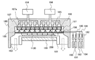
チャンバーに材料ガスとしてモノシランガス(SiH4)と亜酸化窒素(N2O)と希ガスを導入し、10Pa〜30Paの圧力下で高密度プラズマを発生させてガラス等の絶縁表面を有する基板上に絶縁膜を形成する。その後、モノシランガスの供給を停止し、大気に曝すことなく亜酸化窒素(N2O)と希ガスとを導入して絶縁膜表面にプラズマ処理を行う。少なくとも亜酸化窒素(N2O)と希ガスとを導入して絶縁膜表面に行われるプラズマ処理は、絶縁膜の成膜より後に行う。上記プロセス順序を経た絶縁膜は、膜厚が薄く、例えば100nm未満であっても信頼性を確保することができる絶縁膜である。 A monosilane gas (SiH 4 ), nitrous oxide (N 2 O), and a rare gas are introduced into the chamber as material gases, and high-density plasma is generated under a pressure of 10 Pa to 30 Pa to form a substrate having an insulating surface such as glass. An insulating film is formed. Thereafter, supply of monosilane gas is stopped, nitrous oxide (N 2 O) and a rare gas are introduced without exposure to the atmosphere, and plasma treatment is performed on the surface of the insulating film. Plasma treatment performed on the surface of the insulating film by introducing at least nitrous oxide (N 2 O) and a rare gas is performed after the formation of the insulating film. The insulating film that has undergone the above process sequence is a thin film that can ensure reliability even when it is less than 100 nm, for example.
絶縁膜の形成は、高密度プラズマ装置により行う。ここでは、高密度プラズマ装置は、1×10¹¹/cm3以上のプラズマ密度を達成できる装置を指している。例えば、3kW〜6kWのマイクロ波電力を印加してプラズマを発生させて、絶縁膜の成膜を行う。 The insulating film is formed by a high density plasma apparatus. Here, the high-density plasma apparatus refers to an apparatus that can achieve a plasma density of 1 × 10 11 / cm 3 or more. For example, plasma is generated by applying microwave power of 3 kW to 6 kW, and an insulating film is formed.
絶縁膜の形成の際、チャンバーに導入するモノシランガス(SiH4)と亜酸化窒素(N2O)との流量比は、1:10から1:200の範囲とする。また、チャンバーに導入する希ガスとしては、ヘリウム、アルゴン、クリプトン、キセノンなどを用いることができるが、中でも安価であるアルゴンを用いることが好ましい。 When forming the insulating film, the flow ratio of monosilane gas (SiH 4 ) and nitrous oxide (N 2 O) introduced into the chamber is in the range of 1:10 to 1: 200. In addition, as the rare gas introduced into the chamber, helium, argon, krypton, xenon, or the like can be used, and among them, argon, which is inexpensive, is preferably used.
また、高密度プラズマ装置により得られた絶縁膜は、一定した厚さの膜形成ができるため段差被覆性に優れている。また、高密度プラズマ装置により得られる絶縁膜は、薄い膜の厚みを精密に制御することができる。 In addition, since the insulating film obtained by the high-density plasma apparatus can form a film with a constant thickness, it has excellent step coverage. In addition, an insulating film obtained by a high-density plasma apparatus can precisely control the thickness of a thin film.
上記プロセス順序を経た絶縁膜は、従来の平行平板型のプラズマCVD装置で得られる絶縁膜とは大きく異なっており、同じエッチャントを用いてエッチング速度を比較した場合において、従来の平行平板型のプラズマCVD装置で得られる絶縁膜の10%以上または20%以上遅く、上記作製方法で得られる絶縁膜は緻密な膜と言える。 The insulating film that has undergone the above process sequence is significantly different from the insulating film obtained by the conventional parallel plate type plasma CVD apparatus. When the etching rates are compared using the same etchant, the conventional parallel plate type plasma is used. Since the insulating film obtained by the CVD apparatus is 10% or more or 20% or more slower than the insulating film, the insulating film obtained by the above manufacturing method can be said to be a dense film.
また、ガラス等の絶縁表面を有する基板上に半導体膜を形成し、該半導体膜上に高密度プラズマ装置により絶縁膜を形成した後、大気に曝すことなく亜酸化窒素(N2O)と希ガスとを導入して絶縁膜表面にプラズマ処理を行う。その後、絶縁膜を介して半導体膜に一導電型を付与する不純物元素を添加する。その後、絶縁膜上に金属電極を形成して容量素子を形成する。 In addition, after a semiconductor film is formed over a substrate having an insulating surface such as glass, and an insulating film is formed over the semiconductor film by a high-density plasma apparatus, nitrous oxide (N 2 O) and rare earth are not exposed to the atmosphere. Plasma treatment is performed on the surface of the insulating film by introducing a gas. After that, an impurity element imparting one conductivity type is added to the semiconductor film through the insulating film. Thereafter, a metal electrode is formed on the insulating film to form a capacitor element.
一導電型を付与する不純物元素はp型の不純物元素であるボロンを用いる。ボロンは、原子半径が小さいため、絶縁膜にほとんどダメージを与えることなく絶縁膜を通過させて半導体膜に添加させることができる。従って、得られる容量素子は、絶縁膜が薄い膜厚であっても高い耐圧を実現することができる。 As the impurity element imparting one conductivity type, boron which is a p-type impurity element is used. Since boron has a small atomic radius, boron can be added to the semiconductor film through the insulating film with little damage to the insulating film. Therefore, the obtained capacitor element can realize a high breakdown voltage even if the insulating film is thin.
また、上記方法によって得られる半導体装置も特徴を有しており、その構成は、同一基板上に薄膜トランジスタと容量とを有し、容量は、絶縁膜を誘電体とし、金属電極と、半導体に一導電型を付与する不純物元素を含む半導体層とを一対の電極として有し、容量の絶縁膜は、薄膜トランジスタのゲート絶縁膜とほぼ同じ膜厚であることを特徴とする半導体装置である。 In addition, the semiconductor device obtained by the above method also has a feature. The structure includes a thin film transistor and a capacitor over the same substrate, and the capacitor has a dielectric film as a dielectric, a metal electrode, and a semiconductor. The semiconductor device includes a semiconductor layer including an impurity element imparting a conductivity type as a pair of electrodes, and the capacitor insulating film has substantially the same thickness as the gate insulating film of the thin film transistor.
例えば、得られた絶縁膜を液晶表示装置のスイッチング素子である薄膜トランジスタのゲート絶縁膜として用いることによって、ゲート絶縁膜の膜厚が30nmであっても、信頼性を確保することができる。さらに得られた絶縁膜を誘電体とし、一対の電極の一方を導電型が付与された半導体膜とし、液晶表示装置の保持容量として用いた場合であっても、信頼性を確保することができる。液晶表示装置の1画素あたりの保持容量は、例えば、約2pF〜約5pFであり、ゲート絶縁膜の膜厚を薄く、且つ品質を向上させることで、容量値を増大することができるために保持容量が占める電極面積を縮小することができ、開口率の向上を図ることができる。発光表示装置においても、1画素あたりの保持容量が必要であり、例えば、約0.2pF〜約0.5pFであるが、同様にゲート絶縁膜の膜厚を薄く、且つ品質を向上させることで、容量値を増大することができるために保持容量が占める電極面積を縮小することができ、開口率の向上を図ることができる。 For example, by using the obtained insulating film as a gate insulating film of a thin film transistor that is a switching element of a liquid crystal display device, reliability can be ensured even when the thickness of the gate insulating film is 30 nm. Further, reliability can be ensured even when the obtained insulating film is a dielectric, and one of the pair of electrodes is a semiconductor film provided with a conductivity type, and is used as a storage capacitor of a liquid crystal display device. . The holding capacity per pixel of the liquid crystal display device is, for example, about 2 pF to about 5 pF, and the holding value is obtained because the capacitance value can be increased by reducing the thickness of the gate insulating film and improving the quality. The electrode area occupied by the capacitance can be reduced, and the aperture ratio can be improved. Even in a light emitting display device, a storage capacitor per pixel is necessary, for example, about 0.2 pF to about 0.5 pF. Similarly, by reducing the thickness of the gate insulating film and improving the quality. Since the capacitance value can be increased, the electrode area occupied by the storage capacitor can be reduced, and the aperture ratio can be improved.
また、フォトダイオードを有するフォトICの増幅回路に用いられる薄膜トランジスタのゲート絶縁膜として用いることによって、ゲート絶縁膜の膜厚が20nmであっても、信頼性を確保することができる。ゲート絶縁膜の膜厚を薄くすることで薄膜トランジスタのしきい値のバラツキが抑えられ、フォトICの消費電力の低減に寄与することができる。 Further, by using it as a gate insulating film of a thin film transistor used in an amplifier circuit of a photo IC having a photodiode, reliability can be ensured even when the thickness of the gate insulating film is 20 nm. By reducing the thickness of the gate insulating film, variation in threshold voltage of the thin film transistor can be suppressed, which can contribute to reduction in power consumption of the photo IC.
また、得られた絶縁膜を誘電体とし、一対の電極の一方を導電型が付与された半導体層とし、薄膜トランジスタを有する無線チップの保持容量部として用いることによって、絶縁膜の膜厚が10nmであっても、信頼性を確保することができる。薄膜トランジスタを有する無線チップは、主に、電源回路、制御回路、記憶回路、共振容量部とを有している。電源回路は、アンテナが受信した交流信号を整流後に平滑化を行い直流電圧を発生させる。また、電源回路は、交流信号を整流後に平滑化を行い電荷を保持するための保持容量部と呼ばれる容量素子を有している。この容量素子は、一対の電極で挟まれた絶縁膜を誘電体としている。また、無線チップには共振容量部等にも別の容量素子が設けられる。これらの容量素子の静電容量が十分でない場合、通信距離の低下や無線チップの非動作を招く恐れがある。容量素子の面積を大きくすれば、十分な静電容量を得ることができるが、無線チップにおいては、結果として集積回路の占める面積サイズが大きくなってしまい、サイズの拡大により消費電力の増大を招く恐れもある。アンテナから得られる電力は限られているため、無線チップにとって消費電力の増大は、通信距離の短縮に繋がる恐れがあるため、大きな問題となる。また、静電容量は、面積だけでなく、絶縁膜の誘電率や膜厚が影響する。従って、絶縁膜の膜厚を10nmとして静電容量の増大を図ることができる。例えば、UHF帯の無線信号を送受信する場合、交流信号を整流後に平滑化を行い電荷を保持するための保持容量部と呼ばれる容量素子の合計容量値は、1nF(1000pF)を超える。 In addition, by using the obtained insulating film as a dielectric, using one of the pair of electrodes as a semiconductor layer with conductivity type, and using it as a storage capacitor portion of a wireless chip having a thin film transistor, the thickness of the insulating film is 10 nm. Even if it exists, reliability can be ensured. A wireless chip including a thin film transistor mainly includes a power supply circuit, a control circuit, a memory circuit, and a resonance capacitor. The power supply circuit rectifies the AC signal received by the antenna and smoothes it to generate a DC voltage. In addition, the power supply circuit includes a capacitor element called a storage capacitor portion for smoothing the AC signal after rectification and holding the charge. In this capacitive element, an insulating film sandwiched between a pair of electrodes is used as a dielectric. The wireless chip is also provided with another capacitor element in the resonance capacitor portion or the like. If the capacitance of these capacitors is not sufficient, there is a risk that the communication distance will be reduced and the wireless chip will not operate. If the area of the capacitor element is increased, sufficient capacitance can be obtained. However, in the wireless chip, the area size occupied by the integrated circuit increases as a result, and the increase in size causes an increase in power consumption. There is also a fear. Since the power that can be obtained from the antenna is limited, an increase in power consumption for the wireless chip is likely to lead to a reduction in communication distance, which is a big problem. In addition, the capacitance is affected not only by the area but also by the dielectric constant and film thickness of the insulating film. Therefore, the capacitance can be increased by setting the thickness of the insulating film to 10 nm. For example, when transmitting and receiving a radio signal in the UHF band, the total capacitance value of a capacitor element called a storage capacitor unit for smoothing an AC signal after rectification and holding a charge exceeds 1 nF (1000 pF).
さらに無線チップに搭載する薄膜トランジスタのゲート絶縁膜の膜厚を薄くすることで薄膜トランジスタのしきい値のバラツキが抑えられ、無線チップの動作電圧及び消費電力の低減を図ることができ、その結果、無線チップの通信距離の延長を実現することができる。 Further, by reducing the thickness of the gate insulating film of the thin film transistor mounted on the wireless chip, variation in threshold voltage of the thin film transistor can be suppressed, and the operating voltage and power consumption of the wireless chip can be reduced. It is possible to extend the communication distance of the chip.
大量生産をする上で大面積ガラス基板等の絶縁表面を有する基板上に無線チップを作製することは製造コスト上、有利である。一方、薄膜トランジスタを有する無線チップは、送受信するための回路をガラス等の絶縁表面を有する基板上に形成する場合、薄膜トランジスタなどを用いて回路を構成すると、デザインルールが微細で3次元に回路を積層できる単結晶シリコンチップに比べ、回路の占める面積が大きくなる短所がある。従って、絶縁膜の膜厚を薄くすることで集積回路の占める面積サイズを縮小でき、且つ、消費電力の低減を図ることができるため、薄膜トランジスタを有する無線チップにおいて特に有効である。 In mass production, it is advantageous in terms of manufacturing cost to manufacture a wireless chip on a substrate having an insulating surface such as a large-area glass substrate. On the other hand, in the case of a wireless chip having a thin film transistor, when a circuit for transmitting and receiving is formed on a substrate having an insulating surface such as glass, when the circuit is formed using a thin film transistor or the like, the design rule is fine and the circuit is laminated three-dimensionally. Compared to a single crystal silicon chip that can be produced, the circuit occupies a large area. Therefore, by reducing the thickness of the insulating film, the area size occupied by the integrated circuit can be reduced and power consumption can be reduced, which is particularly effective in a wireless chip having a thin film transistor.
上述したこれらの手段は単なる設計事項ではなく、高密度プラズマ装置を用いて絶縁膜を形成し、その絶縁膜を用いた薄膜トランジスタやキャパシタを含む半導体装置を作製し、その半導体装置の信頼性試験を繰り返し行い、発明者らの深い検討の後、発明された事項である。 These means described above are not merely design matters, an insulating film is formed using a high-density plasma device, a semiconductor device including a thin film transistor and a capacitor using the insulating film is manufactured, and a reliability test of the semiconductor device is performed. This is a matter that has been invented after repeated investigations by the inventors.
本明細書において、上、下、側、水平、垂直等の方向を表す文言は、基板表面の上にデバイスを配置した場合の基板面を基準とする方向を指す。 In this specification, the terms representing directions such as up, down, side, horizontal, and vertical refer to directions that are based on the substrate surface when a device is arranged on the substrate surface.
また、本明細書において使用した程度を表す用語、例えば「ほぼ」、「約」などは、最終結果が顕著には変化しないように幾分変更された用語の合理的な逸脱の程度を意味する。これらの用語は、幾分変更された用語の少なくとも±5%の逸脱を含むものとして解釈されるべきであるが、この逸脱が幾分変更される用語の意味を否定しないことを条件とする。 Also, terms representing the degree used in this specification, such as “approximately”, “about”, etc., mean a reasonable degree of deviation of a term that has been slightly modified so that the final result does not change significantly. . These terms should be construed as including at least ± 5% deviation of the somewhat modified term, provided that this deviation does not deny the meaning of the somewhat modified term.
高密度プラズマ装置を用いてガラス等の絶縁表面を有する基板上に低い基板温度で得られる絶縁膜は、窒素を含む酸化珪素膜であり、平行平板型のプラズマCVD装置で得られる膜よりも緻密な薄膜が得られる。また、ガラス等の絶縁表面を有する同一基板上に低い基板温度で得られる高品質の絶縁膜を誘電体とするキャパシタと、高品質の絶縁膜をゲート絶縁膜とする薄膜トランジスタとを有する半導体装置を実現できる。 An insulating film obtained at a low substrate temperature on a substrate having an insulating surface such as glass using a high-density plasma apparatus is a silicon oxide film containing nitrogen, which is denser than a film obtained by a parallel plate type plasma CVD apparatus. A thin film can be obtained. In addition, a semiconductor device having a capacitor using a high-quality insulating film obtained as a dielectric on a same substrate having an insulating surface such as glass as a dielectric, and a thin film transistor using a high-quality insulating film as a gate insulating film realizable.
実施の形態について、以下に説明する。 Embodiments will be described below.
ガラス等の絶縁表面を有する基板上に半導体層を覆う薄い絶縁膜を形成する作製手順フローを図1に示す。 A manufacturing procedure flow for forming a thin insulating film covering a semiconductor layer over a substrate having an insulating surface such as glass is shown in FIG.
半導体層が設けられたガラス基板を高密度プラズマ装置(周波数が1GHz以上、ここでは2.45GHzのマイクロ波プラズマCVD装置)の処理容器内に搬送する。 The glass substrate provided with the semiconductor layer is transferred into a processing container of a high-density plasma apparatus (a microwave plasma CVD apparatus having a frequency of 1 GHz or more, here 2.45 GHz).
ここで、高密度プラズマ装置の一例の上面図を図2に示す。共通室1120は、ロード・アンロード(L/UL)室1110、1115、及び反応室(1)〜反応室(4)1111〜1114とゲート弁1122〜1127を介して連結されている。基板1130は、ロード・アンロード(L/UL)室1110、1115のカセット1128、1129に装填され、共通室1120の搬送手段1121により各反応室に搬送される。
Here, a top view of an example of the high-density plasma apparatus is shown in FIG. The
なお、図2に示す高密度プラズマCVD装置には、ロード・アンロード(L/UL)室が複数設けられているが、一つでもよい。また、高密度プラズマCVD装置に予備室を設けてもよい。予備室で基板を予備加熱することで、各反応室において成膜までの加熱時間を短縮することが可能であるため、スループットを向上させることができる。 In the high-density plasma CVD apparatus shown in FIG. 2, a plurality of load / unload (L / UL) chambers are provided, but one may be used. Further, a preliminary chamber may be provided in the high-density plasma CVD apparatus. By preheating the substrate in the preliminary chamber, the heating time until film formation in each reaction chamber can be shortened, so that the throughput can be improved.
図3は、このような高密度プラズマCVD装置の一つの反応室の構成の一例を詳細に説明するものである。図3は断面図であり、一つの反応室には、処理容器180、処理容器180内に設けられ基板1130を配置するための支持台181、処理容器180内にガスを導入するためのガス供給部182、処理容器180内のガスを排気するために真空ポンプに接続する排気口183、プラズマ発生用のマイクロ波を供給するマイクロ波発生装置184、マイクロ波供給部からマイクロ波を処理容器180に導入する導波管185、導波管185に接し且つ開口部187aを有する天板187、取り付け具188で天板187に設けられた複数の誘電体板186が設けられる。
FIG. 3 illustrates an example of the configuration of one reaction chamber of such a high-density plasma CVD apparatus in detail. FIG. 3 is a cross-sectional view. In one reaction chamber, a
また、基板1130及び誘電体板186の間に着火用ガスを流すガス管197、及び原料ガスを流すガス管198が設けられる。ガス管197、198は、ガス供給部182と接続される。具体的には、着火用ガスを流すガス管197は、バルブ196及び質量流量コントローラ194を介して着火用ガス供給源192に接続される。また、原料ガスを流すガス管198は、バルブ195及び質量流量コントローラ193を介して原料ガス供給源191に接続される。また、支持台181に温度制御部199を設けることによって、基板1130の温度を制御することも可能である。また、支持台181に高周波電源を接続し、高周波電源から出力された交流の電力により、支持台181に所定のバイアス電圧を印加する構成としてもよい。なお、ガス供給部182及びマイクロ波発生装置184は処理容器の外に設けられる。
A
マイクロ波発生装置184は、周波数が1GHz以上、好ましくは2.45GHzまたは8.3GHzのマイクロ波を供給する。なお、マイクロ波発生装置184を複数有することで、安定な大面積のプラズマを生成することが可能である。このため、一辺が600mmを超える基板、特に一辺が1000mmを超える大面積基板においても、均一性の高い膜を成膜する事が可能であり、且つ成膜速度を高めることができる。
The
誘電体板186は、天板187の開口部に密着するように設けられる。マイクロ波発生装置184で発生したマイクロ波が導波管185及び天板187の開口部を経て、誘電体板186に伝播し、誘電体板186を透過して処理容器内に放出される。処理容器内に放出されたマイクロ波の電界エネルギーにより、着火用ガスがプラズマ化する。当該プラズマ200は、誘電体板186表面でより密度が高いため、基板1130へのダメージを低減することができる。また、誘電体板186を複数設けることで、均一な大面積のプラズマの発生及び維持が可能である。なお、誘電体板186は、プラズマ200発生側に窪みが形成されてもよい。当該窪みにより、安定したプラズマを生成することができる。
The
ガス管197、198は、着火用ガスを流すガス管197と原料ガスを流すガス管198が交差して設けられており、着火用ガスを流すガス管197の吹出し口が誘電体板186側に設けられ、原料ガスを流すガス管198の吹出し口が基板1130側に設けられる。着火用ガスが誘電体板186側に噴出されることにより、誘電体板186表面での成膜を回避しつつプラズマ200を発生させることができる。また、基板1130により近い位置で原料ガスを噴出すことが可能であり、成膜速度を高めることが可能である。ガス管197、198は、アルミナ、窒化アルミニウム等のセラミックスで形成される。セラミックスはマイクロ波の透過率が高いため、ガス管197、198をセラミックスで形成することで、誘電体板186の直下にガス管を設けても、電界の乱れが生じずプラズマの分布を均一にすることができる。
The
図2及び図3に示す高密度プラズマ装置を用いた成膜処理の手順を以下に示す。まず、図1のステップS170から成膜処理を開始し、ステップS171にて、基板を加熱する。基板は室温、若しくは温度制御部により100℃〜550℃に加熱する。 The procedure of the film forming process using the high-density plasma apparatus shown in FIGS. 2 and 3 is shown below. First, the film forming process is started from step S170 in FIG. 1, and the substrate is heated in step S171. The substrate is heated to 100 ° C. to 550 ° C. at room temperature or by a temperature control unit.
ステップS172にて処理容器内を真空にし、プラズマ着火用ガスとして、ヘリウム、アルゴン、キセノン、クリプトン等の希ガスのいずれか一種以上及び酸素ガスを導入する。2.45GHzの周波数を用いる場合、希ガスと共に、酸素ガスを処理容器内に導入することで、プラズマの着火を容易とすることができる。なお、周波数などのプラズマ発生条件を適宜設定することで、酸素ガスを用いることなく、希ガスと亜酸化窒素を処理容器内に導入することでプラズマの着火を行うこともできる。この場合、使用するガス種を削減することができる。 In step S172, the inside of the processing chamber is evacuated, and one or more rare gases such as helium, argon, xenon, krypton, and oxygen gas are introduced as plasma ignition gas. When a frequency of 2.45 GHz is used, plasma can be easily ignited by introducing oxygen gas into the processing container together with the rare gas. Note that plasma can be ignited by introducing a rare gas and nitrous oxide into a processing vessel without using oxygen gas by appropriately setting plasma generation conditions such as frequency. In this case, the gas type to be used can be reduced.
次に、ステップS173にて、処理容器内の圧力を所定の圧力にする。処理容器内の圧力は1〜200Pa、好ましくは10〜20Paとする。次に、ステップS174にて、マイクロ波発生装置の電源をオンにし、マイクロ波発生装置から導波管にマイクロ波を供給し、処理容器内でプラズマを生成する。マイクロ波発生装置の出力は500〜6000W、好ましくは4000〜6000Wとする。マイクロ波の導入によりプラズマの励起を行うと、低電子温度(0.7eV以上3eV以下、好ましくは0.7eV以上1.5eV以下)で高電子密度(1×10¹¹〜1×1013cm−3以上)のプラズマを生成することができる。 Next, in step S173, the pressure in the processing container is set to a predetermined pressure. The pressure in the processing vessel is 1 to 200 Pa, preferably 10 to 20 Pa. Next, in step S174, the microwave generator is turned on, microwaves are supplied from the microwave generator to the waveguide, and plasma is generated in the processing container. The output of the microwave generator is 500 to 6000 W, preferably 4000 to 6000 W. When excitation of plasma is performed by introducing a microwave, high electron density (1 × 10 11 to 1 × 10 13 cm − is achieved at a low electron temperature (0.7 eV to 3 eV, preferably 0.7 eV to 1.5 eV). 3 or more) can be generated.
次に、ステップS175にて、ガス管から原料ガスを処理容器内に導入する。具体的には、酸素ガスの供給を停止し、原料ガスとして、亜酸化窒素、及び希ガスを導入した後、亜酸化窒素、希ガス、及び珪素化合物ガスを導入することで、基板上に半導体層を覆う酸化珪素膜を形成することができる。具体的には、原料ガスは、シランに対する亜酸化窒素の流量比を10倍以上300倍以下、好ましくは50倍とする。 Next, in step S175, the source gas is introduced into the processing container from the gas pipe. Specifically, the supply of oxygen gas is stopped, and after introducing nitrous oxide and a rare gas as source gases, a semiconductor is formed on the substrate by introducing nitrous oxide, a rare gas, and a silicon compound gas. A silicon oxide film covering the layer can be formed. Specifically, the source gas has a flow ratio of nitrous oxide to silane of 10 to 300 times, preferably 50 times.
次に、ステップS176にて、原料ガスの供給を停止し、処理容器内の圧力を低下し、マイクロ波発生装置の電源をオフにする。 Next, in step S176, the supply of the raw material gas is stopped, the pressure in the processing container is reduced, and the microwave generator is turned off.
次に、ステップS177にて、プラズマ着火用ガスとして、ヘリウム、アルゴン、キセノン、クリプトン等の希ガスのいずれか一種以上及び酸素ガスを導入する。 Next, in step S177, one or more kinds of rare gases such as helium, argon, xenon, krypton and oxygen gas are introduced as plasma ignition gas.
次に、ステップS178にて、処理容器内の圧力を所定の圧力にする。 Next, in step S178, the pressure in the processing container is set to a predetermined pressure.
次に、ステップS179にて、マイクロ波発生装置の電源をオンにし、マイクロ波発生装置から導波管にマイクロ波を供給し、処理容器内でプラズマを生成する。 Next, in step S179, the microwave generator is turned on, microwaves are supplied from the microwave generator to the waveguide, and plasma is generated in the processing container.
次に、ステップS180にて、ガス管から原料ガスを処理容器180内に導入する。具体的には、酸素ガスの供給を停止し、原料ガスとして、亜酸化窒素及び希ガスを導入することで、酸化珪素膜の表面に対してプラズマ処理を行う。
Next, in step S180, the source gas is introduced into the
次に、ステップS181にて、原料ガスの供給を停止し、処理容器内の圧力を低下し、マイクロ波発生装置の電源をオフにして、ステップS182で成膜プロセスを終了する。そして、基板を処理容器外に搬送する。 Next, in step S181, the supply of the source gas is stopped, the pressure in the processing container is reduced, the power of the microwave generator is turned off, and the film forming process is ended in step S182. Then, the substrate is transferred out of the processing container.
こうして得られる窒素を含む酸化珪素膜を薄膜トランジスタのゲート絶縁膜やキャパシタの誘電体などに用いた場合、半導体素子の耐圧を高めることができる。 When the silicon oxide film containing nitrogen thus obtained is used for a gate insulating film of a thin film transistor or a dielectric of a capacitor, the breakdown voltage of the semiconductor element can be increased.
得られた絶縁膜の耐圧を測定するため、以下に示す実験を行った。 In order to measure the withstand voltage of the obtained insulating film, the following experiment was conducted.
サンプルの作製手順を示す。まず、ガラス基板上に平行平板型のプラズマCVD装置を用いてアモルファスシリコン膜を成膜し、波長が532nmのレーザ光(500μmの長軸ビーム幅)を走査(スキャン速度350mm/s)し、結晶化させポリシリコン膜を形成する。なお、レーザ照射前には酸化膜をフッ酸を含むエッチャントを用いてウエットエッチングで除去する。 The preparation procedure of the sample is shown. First, an amorphous silicon film is formed on a glass substrate using a parallel plate type plasma CVD apparatus, a laser beam having a wavelength of 532 nm (long axis beam width of 500 μm) is scanned (scanning speed 350 mm / s), and a crystal To form a polysilicon film. Note that before laser irradiation, the oxide film is removed by wet etching using an etchant containing hydrofluoric acid.
次いで、ポリシリコン膜を選択的にエッチングして島状半導体層を形成した後、島状半導体層を覆うように、高密度プラズマ装置を用いて絶縁膜を形成する。 Next, the polysilicon film is selectively etched to form an island-shaped semiconductor layer, and then an insulating film is formed using a high-density plasma apparatus so as to cover the island-shaped semiconductor layer.
なお、絶縁膜の形成前に高密度プラズマ装置を用いてプラズマ処理を行う。4台のマイクロ波発生装置(4.5kW)を有する高密度プラズマ装置を用いる。プラズマ処理は、圧力20Pa、基板温度325℃、ギャップ間隔(誘電体−基板間隔)160mm、亜酸化窒素の流量1000sccm、アルゴン流量2500sccmとして5分間行った。次いで、圧力20Pa、基板温度325℃、ギャップ間隔(誘電体−基板間隔)160mm、モノシランの流量30sccm、亜酸化窒素の流量1500sccm、アルゴンの流量2500sccmとして膜厚10nmの絶縁膜を成膜した。成膜後、再度、成膜前に行ったプラズマ処理と同じ条件のプラズマ処理を行った。 Note that plasma treatment is performed using a high-density plasma apparatus before formation of the insulating film. A high-density plasma apparatus having four microwave generators (4.5 kW) is used. The plasma treatment was performed for 5 minutes at a pressure of 20 Pa, a substrate temperature of 325 ° C., a gap interval (dielectric-substrate interval) of 160 mm, a nitrous oxide flow rate of 1000 sccm, and an argon flow rate of 2500 sccm. Next, an insulating film having a thickness of 10 nm was formed with a pressure of 20 Pa, a substrate temperature of 325 ° C., a gap interval (dielectric-substrate interval) of 160 mm, a monosilane flow rate of 30 sccm, a nitrous oxide flow rate of 1500 sccm, and an argon flow rate of 2500 sccm. After film formation, plasma treatment under the same conditions as the plasma treatment performed before film formation was performed again.
次いで、絶縁膜を通過させて絶縁膜と重なる半導体層にボロンをドーピングする。加速電圧は20kVとし、1×10¹⁹/cm3以上1×1020/cm3未満の濃度となるドーピング処理を行う。 Next, boron is doped into the semiconductor layer which passes through the insulating film and overlaps with the insulating film. The accelerating voltage is 20 kV, and a doping process is performed to achieve a concentration of 1 × 10 19 / cm 3 or more and less than 1 × 10 20 / cm 3 .
次いで、半導体層と重なる絶縁膜上に電極を形成し、電極をマスクとしてボロンを半導体層に添加する。なお、添加されるボロンは、1×10²⁰/cm3以上1×1022/cm3未満の濃度となるドーピング処理を行う。 Next, an electrode is formed over the insulating film overlapping the semiconductor layer, and boron is added to the semiconductor layer using the electrode as a mask. Note that boron to be added is subjected to a doping treatment to a concentration of 1 × 10 20 / cm 3 or more and less than 1 × 10 22 / cm 3 .
また、絶縁膜を通過させて半導体層にボロンを添加した上記サンプルとは異なる工程順序、具体的には絶縁膜を形成する前にドーピングを行ったサンプルを作製し、絶縁破壊が生じるまで電圧を与え、その分布を示すグラフを図4(A)に示す。 In addition, a process sequence different from the above sample in which boron is added to the semiconductor layer through the insulating film, specifically, a sample that is doped before forming the insulating film is prepared, and the voltage is applied until dielectric breakdown occurs. A graph showing the distribution is shown in FIG.
また、図4(A)は、ドーピングの加速電圧の条件も振った結果も含んでいる。また、ボロンに代えてリンをドーピングしたサンプルの結果も含んでいる。図4(A)の結果から、絶縁膜の形成前にドーピングを行うサンプルよりも絶縁膜を通過させて半導体層にドーピングするサンプルのほうが、破壊される電圧値が高く、高い耐圧を有している傾向が読み取れる。また、ドーピング処理の加速電圧が低いほうが、破壊される電圧値が高く、高い耐圧を有している傾向が読み取れる。 FIG. 4A also includes the result of varying the conditions of the accelerating voltage for doping. It also includes the results for samples doped with phosphorus instead of boron. From the result of FIG. 4A, the sample in which the semiconductor layer is doped by passing through the insulating film has a higher breakdown voltage value and higher breakdown voltage than the sample in which doping is performed before the insulating film is formed. I can read the tendency. Further, it can be seen that the lower the accelerating voltage of the doping process, the higher the breakdown voltage value and the higher the withstand voltage.
また、図4(A)からは、電極と重なる半導体層にリンをドーピングしたサンプルよりも電極と重なる半導体層にボロンをドーピングしたサンプルのほうが、破壊される電圧値が高い傾向が読み取れる。このことは、イオン種がリンの場合では絶縁膜にドーピングによるダメージが入ってしまうが、ボロンでは原子サイズがリンより小さいためダメージを低減できていることに起因している。 From FIG. 4A, it can be seen that the sample in which the semiconductor layer overlapping with the electrode is doped with boron has a higher breakdown voltage value than the sample in which the semiconductor layer overlapping with the electrode is doped with phosphorus. This is because, when the ion species is phosphorus, the insulating film is damaged by doping, but since boron has an atomic size smaller than phosphorus, the damage can be reduced.
また、図4(A)とは異なる半導体層の上面形状、具体的には電極と重なる半導体層を短冊状に形成したサンプルの結果を図4(B)に示す。図4(B)で特筆すべきは、絶縁膜を介してボロンをドーピングしたサンプルに関しては、図4(A)とほぼ同じ結果を示していることである。このことは、半導体層が短冊状であれば、その上に形成される絶縁膜にも凹凸が形成されることになるが、本実施の形態に示す作製方法により、膜厚10nmと薄い絶縁膜であっても均一な膜厚が短冊状の半導体層上に被覆性良く形成されていると言える。 FIG. 4B shows the result of a sample in which the top surface shape of a semiconductor layer different from that in FIG. 4A, specifically, a semiconductor layer overlapping with an electrode is formed in a strip shape. It should be noted in FIG. 4B that the sample doped with boron through the insulating film shows almost the same result as in FIG. This means that if the semiconductor layer is strip-shaped, irregularities are also formed on the insulating film formed thereon, but with the manufacturing method described in this embodiment, a thin insulating film with a thickness of 10 nm is formed. Even so, it can be said that a uniform film thickness is formed on the strip-shaped semiconductor layer with good coverage.
なお、図4(A)、図4(B)では、絶縁膜の成膜の前後にプラズマ処理を行った例を示しているが特に限定されず、例えば、さらなる高信頼性を得るためには、絶縁膜の成膜後のみにプラズマ処理を行うことが好ましい。 4A and 4B show an example in which plasma treatment is performed before and after the formation of the insulating film, but there is no particular limitation. For example, in order to obtain higher reliability The plasma treatment is preferably performed only after the insulating film is formed.
また、ドーピング処理の加速電圧が低いほうが、I−V特性のバラツキも低減する。図5にI−V特性を示すグラフを示す。図5(A)は、電極と重なる短冊状の半導体層にリンを10kVでドーピングしたサンプルのI−V特性のバラツキを示す実験結果であり、図5(B)は、電極と重なる短冊状の半導体層にリンを20kVでドーピングしたサンプルのI−V特性のバラツキを示す実験結果である。 Also, the lower the accelerating voltage of the doping process, the less the variation in IV characteristics. FIG. 5 shows a graph showing the IV characteristics. FIG. 5A shows experimental results showing variations in IV characteristics of a sample in which phosphorus is doped at 10 kV on a strip-shaped semiconductor layer that overlaps with the electrode. FIG. 5B shows a strip-shaped layer that overlaps with the electrode. It is an experimental result which shows the variation in the IV characteristic of the sample which doped the semiconductor layer with phosphorus at 20 kV.
また、絶縁膜の成膜後のパーティクル数の圧力依存性を測定した結果を図6に示す。成膜条件は、成膜温度325℃、ギャップ間隔160mm、シラン30sccm、亜酸化窒素の流量3000sccm、アルゴンの流量2500sccmとして膜厚10nmの絶縁膜を成膜した。成膜圧力を20Paと30Paとでパーティクル数の比較を行っている。図6に示すように30Paよりも20Paのほうがパーティクル数が少なく、好ましい圧力条件であることが分かる。図6の成膜条件においてシランに対する亜酸化窒素の流量比は、100倍であり、50倍に比べてパーティクル数が多く発生する条件である。パーティクルが多く発生すると、絶縁膜表面に微小な凸部が形成される恐れがあり、膜厚均一性が低下する。 Further, FIG. 6 shows the result of measuring the pressure dependency of the number of particles after forming the insulating film. The film formation conditions were as follows: an insulating film having a film thickness of 325 ° C., a gap interval of 160 mm, a silane of 30 sccm, a nitrous oxide flow rate of 3000 sccm, and an argon flow rate of 2500 sccm was formed. The number of particles is compared at a film forming pressure of 20 Pa and 30 Pa. As shown in FIG. 6, it can be seen that 20 Pa is less in number of particles than 30 Pa, which is a preferable pressure condition. In the film forming conditions of FIG. 6, the flow rate ratio of nitrous oxide to silane is 100 times, and the number of particles is larger than 50 times. If a large number of particles are generated, there is a possibility that minute convex portions are formed on the surface of the insulating film, and the film thickness uniformity is lowered.
ここでは、膜厚10nmの絶縁膜を用いて比較した例を説明したが、特にこの膜厚に限定されず、100nm未満の薄い膜厚であれば同様の効果が得られる。勿論、膜厚が薄ければ薄いほど成膜に要する時間を短縮することができる。また、高密度プラズマ装置を用いた絶縁膜を誘電体とする容量を形成する場合、絶縁膜の膜厚が薄ければ薄いほど大きな容量を形成することができる。 Here, although the example compared using the 10-nm-thick insulating film was demonstrated, it is not specifically limited to this film thickness, The same effect will be acquired if it is a thin film thickness of less than 100 nm. Of course, the thinner the film thickness, the shorter the time required for film formation. Further, in the case of forming a capacitor using an insulating film as a dielectric using a high-density plasma apparatus, the thinner the insulating film, the larger the capacitance can be formed.
また、高密度プラズマ装置を用いて、シリコンウエハ上に第1の絶縁膜、第2の絶縁膜、第3の絶縁膜、第4の絶縁膜、第5の絶縁膜をそれぞれ200nmの膜厚で積層し、SIMS(二次イオン質量分析計)を用いた分析により、膜中の水素、炭素、窒素、及びフッ素の濃度を測定した結果を図7に示す。第1の絶縁膜の成膜条件は、圧力を20Paとし、シラン流量を30sccmとし、亜酸化窒素の流量を1500sccmとしてシランに対する亜酸化窒素の流量比を50倍とした。また、第2の絶縁膜の成膜条件は、圧力を20Paとし、シラン流量を60sccmとし、亜酸化窒素の流量を3000sccmとしてシランに対する亜酸化窒素の流量比を50倍とした。また、第3の絶縁膜の成膜条件は、圧力を30Paとし、シラン流量を100sccm、亜酸化窒素を流量3000sccmとしてシランに対する亜酸化窒素の流量比を30倍とした。また、第4の絶縁膜の成膜条件は、圧力を30Paとし、シラン流量を250sccm、亜酸化窒素の流量を2500sccmとしてシランに対する亜酸化窒素の流量比を10倍としている。なお、第1、第2、第3、第4の絶縁膜は、流量2500sccmのアルゴンガスを誘電体板側に噴出させ、原料ガス(シラン及び亜酸化窒素)を基板側に噴出させた。また、第5の絶縁膜は酸化珪素膜のリファレンスである。第5の絶縁膜の成膜条件は、圧力を15Paとし、シラン流量を250sccm、酸素の流量を1500sccm、アルゴンガスの流量を3500sccmとして全てのガスを基板側に噴出させた。また、第1、第2、第3、第4、第5の絶縁膜は、基板温度を325℃とし、ギャップ間隔を160mmとした。図7からは、シランと、亜酸化窒素とを成膜ガスとし、高密度プラズマ装置を用いて得られる絶縁膜の窒素濃度が、1×1019/cm3以上1×1021/cm3未満であることが読み取れる。本実施の形態では、上述した第1、第2、第3、第4のいずれか一の絶縁膜に対して成膜室と同じチャンバーで大気に曝すことなく連続的に、亜酸化窒素を用いたプラズマ処理を行うことで、さらなる絶縁膜の表面改質を行っている。また、本明細書における濃度は、SIMSを用いた分析による濃度のピーク値を指している。SIMSは濃度の低い側から高い側に向かって深さ方向に分析された値である。 Further, using a high-density plasma apparatus, a first insulating film, a second insulating film, a third insulating film, a fourth insulating film, and a fifth insulating film are each formed to a thickness of 200 nm on a silicon wafer. FIG. 7 shows the results of measuring the concentrations of hydrogen, carbon, nitrogen, and fluorine in the film by stacking and analyzing using SIMS (secondary ion mass spectrometer). The conditions for forming the first insulating film were as follows: the pressure was 20 Pa, the silane flow rate was 30 sccm, the nitrous oxide flow rate was 1500 sccm, and the flow rate ratio of nitrous oxide to silane was 50 times. The second insulating film was formed under the following conditions: the pressure was 20 Pa, the silane flow rate was 60 sccm, the nitrous oxide flow rate was 3000 sccm, and the flow rate ratio of nitrous oxide to silane was 50 times. The third insulating film was formed under the following conditions: the pressure was 30 Pa, the silane flow rate was 100 sccm, the nitrous oxide flow rate was 3000 sccm, and the flow rate ratio of nitrous oxide to silane was 30 times. The fourth insulating film is formed under the following conditions: the pressure is 30 Pa, the silane flow rate is 250 sccm, the flow rate of nitrous oxide is 2500 sccm, and the flow rate ratio of nitrous oxide to silane is 10 times. For the first, second, third, and fourth insulating films, argon gas having a flow rate of 2500 sccm was jetted to the dielectric plate side, and source gases (silane and nitrous oxide) were jetted to the substrate side. The fifth insulating film is a reference for the silicon oxide film. The conditions for forming the fifth insulating film were as follows: the pressure was 15 Pa, the silane flow rate was 250 sccm, the oxygen flow rate was 1500 sccm, and the argon gas flow rate was 3500 sccm. The first, second, third, fourth, and fifth insulating films have a substrate temperature of 325 ° C. and a gap interval of 160 mm. From FIG. 7, the nitrogen concentration of the insulating film obtained by using silane and nitrous oxide as a deposition gas and using a high-density plasma apparatus is 1 × 10 19 / cm 3 or more and less than 1 × 10 21 / cm 3. It can be read that. In this embodiment, nitrous oxide is continuously used for any one of the first, second, third, and fourth insulating films described above without being exposed to the atmosphere in the same chamber as the film formation chamber. The surface treatment of the insulating film is further performed by performing the plasma treatment. In addition, the concentration in the present specification indicates a peak value of the concentration by analysis using SIMS. SIMS is a value analyzed in the depth direction from the lower concentration side to the higher side.
以上の構成でなる実施の形態について、以下に示す実施例でもってさらに詳細な説明を行うこととする。 The embodiment having the above configuration will be described in more detail with the following examples.
本実施例では、アンテナ回路を含む半導体装置を基板上に設ける構成について説明する。 In this embodiment, a structure in which a semiconductor device including an antenna circuit is provided over a substrate will be described.
まず、図8(A)に示すように、基板1901の一表面に絶縁膜1902を介して剥離層1903を形成し、続けて下地膜として機能する絶縁膜1904と半導体膜1905(例えば、非晶質珪素を含む膜)を積層して形成する。なお、絶縁膜1902、剥離層1903、絶縁膜1904および半導体膜1905は、連続して形成することができる。
First, as illustrated in FIG. 8A, a
なお、基板1901は、ガラス基板、石英基板、金属基板(例えばステンレス基板など)、セラミック基板から選択されるものである。なお、本工程では、剥離層1903は、絶縁膜1902を介して基板1901の全面に設けているが、必要に応じて、基板1901の全面に剥離層を設けた後に、フォトリソグラフィ法により選択的に設けてもよい。
Note that the
また、絶縁膜1902、絶縁膜1904は、プラズマCVD法やスパッタリング法等を用いて、酸化シリコン、窒化シリコン、酸化窒化シリコン(SiOxNy)(x>y>0)、窒化酸化シリコン(SiNxOy)(x>y>0)等の材料を用いて形成する。例えば、絶縁膜1902、1904を2層構造とする場合、第1層目の絶縁膜として窒化酸化シリコン膜を形成し、第2層目の絶縁膜として酸化窒化シリコン膜を形成するとよい。また、第1層目の絶縁膜として窒化シリコン膜を形成し、第2層目の絶縁膜として酸化シリコン膜を形成してもよい。絶縁膜1902は、基板1901から剥離層1903またはその上に形成される素子に不純物元素が混入するのを防ぐブロッキング層として機能し、絶縁膜1904は基板1901、剥離層1903からその上に形成される素子に不純物元素が混入するのを防ぐブロッキング層として機能する。このように、ブロッキング層として機能する絶縁膜1902、1904を形成することによって、基板1901からNaなどのアルカリ金属やアルカリ土類金属が、剥離層1903から剥離層に含まれる不純物元素がこの上に形成する素子に悪影響を与えることを防ぐことができる。なお、基板1901として石英を用いるような場合には絶縁膜1902、1904を省略してもよい。
The insulating
また、剥離層1903は、金属膜や金属膜と金属酸化膜の積層構造等を用いることができる。金属膜としては、タングステン(W)、モリブデン(Mo)、チタン(Ti)、タンタル(Ta)、ニオブ(Nb)、ニッケル(Ni)、コバルト(Co)、ジルコニウム(Zr)、亜鉛(Zn)、ルテニウム(Ru)、ロジウム(Rh)、パラジウム(Pd)、オスミウム(Os)、イリジウム(Ir)から選択された元素または当該元素を主成分とする合金材料若しくは化合物材料からなる膜を単層または積層して形成する。また、これらの材料は、スパッタ法やプラズマCVD法等を用いて形成することができる。金属膜と金属酸化膜の積層構造としては、上述した金属膜を形成した後に、酸素雰囲気下または酸化窒素雰囲気下におけるプラズマ処理、酸素雰囲気下または酸化窒素雰囲気下における加熱処理を行うことによって、金属膜表面に当該金属膜の酸化物または酸化窒化物を設けることができる。例えば、金属膜としてスパッタ法やCVD法等によりタングステン膜を設けた場合、タングステン膜にプラズマ処理を行うことによって、タングステン膜表面にタングステン酸化物からなる金属酸化膜を形成することができる。他にも、例えば、金属膜(例えば、タングステン)を形成した後に、当該金属膜上にスパッタ法で酸化珪素等の絶縁膜を設けると共に、金属膜上に金属酸化物(例えば、タングステン上にタングステン酸化物)を形成してもよい。また、プラズマ処理として、例えば高密度プラズマ装置を用いた高密度プラズマ処理を行ってもよい。また、金属酸化膜の他にも、金属窒化物や金属酸化窒化物を用いてもよい。この場合、金属膜に窒素雰囲気下または窒素と酸素雰囲気下でプラズマ処理や加熱処理を行えばよい。
For the
また、半導体膜1905は、スパッタリング法、LPCVD法、プラズマCVD法等により、25nm以上200nm以下(好ましくは30nm以上150nm以下)の厚さで形成する。
The
次に、図8(B)に示すように、半導体膜1905にレーザビームを照射して結晶化を行う。なお、レーザビームの照射と、RTAまたはファーネスアニール炉を用いる熱結晶化法、結晶化を助長する金属元素を用いる熱結晶化法とを組み合わせた方法等により半導体膜1905の結晶化を行ってもよい。
Next, as shown in FIG. 8B, the
結晶化工程の一例を以下に簡単に説明すると、まず、平行平板型のプラズマCVD装置を用いて非晶質半導体膜を成膜し、膜厚66nmとする。その後、メガヘルツレーザビームを照射し、結晶質半導体膜1905を形成する。なお、本明細書においてメガヘルツレーザビームとは、周波数10MHz以上、パルス幅100fs以上1ns以下の極短パルスを有するレーザビームを言う。周波数を10MHz以上とすることで、連続的に半導体膜に熱を与えることができるため、連続的な結晶成長が可能となる。本実施例では、メガヘルツレーザビーム照射前に酸化膜除去を行った後、周波数80MHz、パルス幅15psのYVO4レーザを用いて、波長532nm、照射パワー8〜9W、長軸ビーム幅500μm、スキャン速度350mm/sとする。照射後の半導体膜の膜厚は60nmとなる。
An example of the crystallization process will be briefly described below. First, an amorphous semiconductor film is formed using a parallel plate type plasma CVD apparatus to a film thickness of 66 nm. After that, irradiation with a megahertz laser beam is performed to form a
半導体膜1905の結晶化の後、フォトリソグラフィ法を用いることによって得られた結晶質半導体膜を所望の形状にエッチングして、結晶質半導体膜1905a、1905b、1905d、1905e、1905fを形成し、当該半導体膜を覆うようにゲート絶縁膜1906を形成する。
After crystallization of the
ゲート絶縁膜1906は、高密度プラズマ装置を用いて形成する。例えば、圧力20Pa、基板温度325℃、ギャップ間隔(誘電体−基板間隔)160mm、モノシランの流量30sccm、亜酸化窒素の流量1500sccm、アルゴンの流量2500sccmとして膜厚10nmの絶縁膜を成膜する。
The
次いで、高密度プラズマ装置を用いてプラズマ処理を行う。プラズマ処理は、圧力20Pa、基板温度325℃、ギャップ間隔(誘電体−基板間隔)160mm、亜酸化窒素の流量1000sccm、アルゴン流量2500sccmとする。このような高密度プラズマを用いた処理により、結晶粒界において異常に酸化反応をさせることなく、均一性が良く、界面準位密度が低い絶縁膜が形成され、その結果、高耐圧である10nmのゲート絶縁膜1906を得ることができる。
Next, plasma treatment is performed using a high-density plasma apparatus. The plasma treatment is performed at a pressure of 20 Pa, a substrate temperature of 325 ° C., a gap interval (dielectric-substrate interval) of 160 mm, a nitrous oxide flow rate of 1000 sccm, and an argon flow rate of 2500 sccm. By the treatment using such high-density plasma, an insulating film having good uniformity and low interface state density is formed without causing an abnormal oxidation reaction at the crystal grain boundary. As a result, a high breakdown voltage of 10 nm is formed. The
本実施例では、ゲート絶縁膜1906の膜厚を10nmとする例を説明したが、特にこの膜厚に限定されず、10nmよりも厚く100nm未満の膜厚であっても、均一性が良く、界面準位密度が低い絶縁膜が得られる。
In this embodiment, the example in which the thickness of the
次に、フォトリソグラフィ法を用いてレジストからなるマスクを形成し、イオンドープ法またはイオン注入法により、保持容量部1900bとなる半導体膜1905bにゲート絶縁膜1906を介してp型を付与する不純物元素を添加する。p型を示す不純物元素としては、ボロン(B)やアルミニウム(Al)やガリウム(Ga)等を用いることができる。ここでは、p型を付与する不純物元素としてボロン(B)を用い、1×10¹⁹/cm3以上1×1020/cm3以下の濃度で含まれるように選択的に添加する。添加した後は、レジストからなるマスクを除去する。
Next, a resist mask is formed by photolithography, and an impurity element imparting p-type conductivity to the
次に、ゲート絶縁膜1906上に、第1の導電膜と第2の導電膜とを積層して形成する。ここでは、第1の導電膜は、CVD法やスパッタリング法等により、20nm以上100nm以下の厚さで形成する。第2の導電膜は、100nm以上400nm以下の厚さで形成する。第1の導電膜と第2の導電膜は、タンタル(Ta)、タングステン(W)、チタン(Ti)、モリブデン(Mo)、アルミニウム(Al)、銅(Cu)、クロム(Cr)、ニオブ(Nb)等から選択された元素、またはこれらの元素を主成分とする合金材料若しくは化合物材料で形成する。または、リン等の不純物元素をドーピングした多結晶珪素に代表される半導体材料により形成する。第1の導電膜と第2の導電膜の組み合わせの例を挙げると、窒化タンタル膜とタングステン膜、窒化タングステン膜とタングステン膜、窒化モリブデン膜とモリブデン膜等が挙げられる。タングステンや窒化タンタルは、耐熱性が高いため、第1の導電膜と第2の導電膜を形成した後に、熱活性化を目的とした加熱処理を行うことができる。また、2層構造ではなく、3層構造の場合は、モリブデン膜とアルミニウム膜とモリブデン膜の積層構造を採用するとよい。
Next, a first conductive film and a second conductive film are stacked over the
次に、フォトリソグラフィ法を用いてレジストからなるマスクを形成し、ゲート電極とゲート線を形成するためのエッチング処理を行って、半導体膜1905a、1905b、1905d、1905e、1905fの上方にゲート電極1907を形成する。ここでは、ゲート電極1907として、第1の導電膜1907aと第2の導電膜1907bの積層構造で設けた例を示している。
Next, a resist mask is formed by photolithography, and an etching process for forming a gate electrode and a gate line is performed, so that the
次に、図8(C)に示すように、ゲート電極1907をマスクとして半導体膜1905a、1905b、1905d、1905e、1905fに、イオンドープ法またはイオン注入法により、n型を付与する不純物元素を低濃度に添加し、その後、フォトリソグラフィ法によりレジストからなるマスクを選択的に形成して、p型を付与する不純物元素を高濃度に半導体膜1905b、1905eに添加する。n型を示す不純物元素としては、リン(P)やヒ素(As)等を用いることができる。ここでは、n型を付与する不純物元素としてリン(P)を用い、1×10¹⁸/cm3以上1×1019/cm3以下の濃度で含まれるように半導体膜1905a、1905b、1905d、1905e、1905fに導入し、n型を示す不純物領域1908を形成する。また、p型を付与する不純物元素としてボロン(B)を用い、1×1018/cm3以上1×1019/cm3以下の濃度で含まれるように選択的に半導体膜1905b、1905eに導入し、p型を示す不純物領域1909を形成する。
Next, as illustrated in FIG. 8C, an impurity element imparting n-type conductivity is reduced in the
続いて、ゲート絶縁膜1906とゲート電極1907を覆うように、絶縁膜を形成する。絶縁膜は、プラズマCVD法やスパッタリング法等により、珪素、珪素の酸化物または珪素の窒化物の無機材料を含む膜、及び有機樹脂などの有機材料を含む膜の一種または複数種を、単層または積層して形成する。次に、絶縁膜を垂直方向を主体とした異方性エッチングにより選択的にエッチングして、ゲート電極1907の側面に接する絶縁膜1910(サイドウォールともよばれる)を形成する。絶縁膜1910は、LDD(Lightly Doped drain)領域を形成する際のドーピング用のマスクとして用いる。
Subsequently, an insulating film is formed so as to cover the
続いて、フォトリソグラフィ法により形成したレジストからなるマスクと、ゲート電極1907および絶縁膜1910をマスクとして用いて、半導体膜1905a、半導体膜1905d、半導体膜1905fにn型を付与する不純物元素を高濃度に添加して、n型を示す高濃度不純物領域1911を形成する。ここでは、n型を付与する不純物元素としてリン(P)を用い、1×10²⁰/cm3以上1×1021/cm3以下の濃度で含まれるように半導体膜1905a、半導体膜1905d、半導体膜1905fに選択的に導入し、不純物領域1908より高濃度のn型を示す高濃度不純物領域1911を形成する。
Next, a high-concentration impurity element imparting n-type conductivity to the
以上の工程により、図8(D)に示すように、nチャネル型である薄膜トランジスタ1900a、1900d、及び1900fと、pチャネル型である薄膜トランジスタ1900eと、保持容量部1900bが形成される。
Through the above steps, as illustrated in FIG. 8D, n-channel
なお、薄膜トランジスタ1900aは、ゲート電極1907と重なる半導体膜1905aの領域にチャネル形成領域が形成され、ゲート電極1907及び絶縁膜1910と重ならない領域にソース領域またはドレイン領域を形成する高濃度不純物領域1911が形成され、絶縁膜1910と重なる領域であってチャネル形成領域と高濃度不純物領域1911の間に低濃度不純物領域(LDD領域)が形成されている。また、薄膜トランジスタ1900d、薄膜トランジスタ1900fも同様にチャネル形成領域、低濃度不純物領域及び高濃度不純物領域1911が形成されている。
Note that the
また、薄膜トランジスタ1900eは、ゲート電極1907と重なる半導体膜1905eの領域にチャネル形成領域が形成され、ゲート電極1907と重ならない領域に高濃度不純物領域1909が形成されている。なお、ここでは、薄膜トランジスタ1900eには、LDD領域を設けていないが、LDD領域を設けてもよいし、薄膜トランジスタ1900aにLDD領域を設けない構成としてもよい。
In the
また、保持容量部1900bは、ゲート電極1907と同じ工程で形成された電極と、半導体膜1905bとを一対の電極とし、膜厚10nmの絶縁膜を誘電体としている。UHF帯の無線信号を送受信する場合、交流信号を整流後に平滑化を行い電荷を保持するための保持容量部の合計容量値は、1nF(1000pF)を超える。ここでは、合計容量値が約30nFとする。
In the
次に、図9(A)に示すように、半導体膜1905a、1905b、1905d、1905e、1905f、ゲート電極1907等を覆うように、絶縁膜を単層または積層を形成し、当該絶縁膜上に高濃度不純物領域1909、1911と電気的に接続する導電膜1913aと、保持容量部と電気的に接続する導電膜1913bを形成する。絶縁膜は、CVD法、スパッタリング法、SOG法、液滴吐出法、スクリーン印刷法等により、珪素の酸化物及び珪素の窒化物等の無機材料、ポリイミド、ポリアミド、ベンゾシクロブテン、アクリル、及びエポキシ等の有機材料、シロキサン材料のいずれか一種または複数種を単層または積層で形成する。ここでは、当該絶縁膜を2層で設け、1層目の絶縁膜1912aとして窒化酸化珪素膜で形成し、2層目の絶縁膜1912bとして酸化窒化珪素膜で形成する。また、導電膜1913aは、半導体膜1905a、1905d、1905e、1905fと電気的に接続するソース電極またはドレイン電極を形成する。
Next, as illustrated in FIG. 9A, an insulating film is formed as a single layer or a stacked layer so as to cover the
なお、絶縁膜1912a、1912bを形成する前、または絶縁膜1912a、1912bのうちの1つまたは複数の薄膜を形成した後に、半導体膜の結晶性の回復や半導体膜に添加された不純物元素の活性化、半導体膜の水素化を目的とした加熱処理を行うとよい。加熱処理には、熱アニール、レーザニール法またはRTA法などを適用するとよい。
Note that before the insulating
また、導電膜1913a、1913bは、CVD法やスパッタリング法等により、アルミニウム、タングステン、チタン、タンタル、モリブデン、ニッケル、白金、銅、金、銀、マンガン、ネオジム、炭素、及びシリコンから選択された元素、またはこれらの元素を主成分とする合金材料または化合物材料で、単層または積層で形成する。アルミニウムを主成分とする合金材料とは、例えば、アルミニウムを主成分とし、ニッケルを含む材料、またはアルミニウムを主成分とし、ニッケルと、炭素と珪素の一方または両方とを含む合金材料などを用いることができる。導電膜1913a、1913bは、例えば、バリア膜とアルミニウムシリコン(Al−Si)膜とバリア膜の積層構造、バリア膜とアルミニウムシリコン(Al−Si)膜と窒化チタン膜とバリア膜の積層構造を採用するとよい。なお、バリア膜とは、チタン、チタンの窒化物、モリブデン、またはモリブデンの窒化物からなる薄膜に相当する。アルミニウムやアルミニウムシリコンは抵抗値が低く、安価であるため、導電膜1913a、1913bを形成する材料として最適である。
The
次に、導電膜1913a、1913bを覆うように、層間絶縁膜1914を形成する。
Next, an
なお、層間絶縁膜1914は、CVD法やスパッタ法等により、酸化珪素、窒化珪素、酸化窒化珪素、窒化酸化珪素等の酸素または窒素を有する絶縁膜やDLC(ダイヤモンドライクカーボン)等の炭素を含む膜、エポキシ、ポリイミド、ポリアミド、ポリビニルフェノール、ベンゾシクロブテン、アクリル等の有機材料またはシロキサン樹脂等のシロキサン材料からなる単層または積層構造で設けることができる。なお、シロキサン材料とは、Si−O−Si結合を含む材料に相当する。シロキサンは、シリコン(Si)と酸素(O)との結合で骨格構造が構成される。置換基として、有機基(例えばアルキル基、芳香族炭化水素基)やフルオロ基を用いてもよい。有機基は、フルオロ基を有してもよい。
Note that the
次に、層間絶縁膜1914上に、薄膜トランジスタ1900a、1900fのソース電極またはドレイン電極を形成する導電膜1913aとそれぞれ電気的に接続する導電膜1915a、1915bを形成する。また、保持容量部1900bの電極と電気的に接続する導電膜1916aを形成する。薄膜トランジスタ1900eのソース電極またはドレイン電極を形成する導電膜1913aと電気的に接続する導電膜1916bを形成する。なお、導電膜1915a、1915bと導電膜1916a、1916bは同一の材料で同時に形成してもよい。導電膜1915a、1915bと導電膜1916a、1916bは、上述した導電膜1913a、1913bに用いることのできる材料のいずれかを用いて形成することができる。
Next,
続いて、図9(B)に示すように、導電膜1916a、1916b上にアンテナとして機能する導電膜1917a、1917bが電気的に接続されるように形成する。
Subsequently, as illustrated in FIG. 9B,
また、導電膜1917a、1917bは、CVD法、スパッタリング法、スクリーン印刷やグラビア印刷等の印刷法、液滴吐出法、ディスペンサ法、メッキ法等を用いて、導電性材料により形成する。導電性材料は、アルミニウム、チタン、銀、銅、金、白金、ニッケル、パラジウム、タンタル、モリブデンから選択された元素、またはこれらの元素を主成分とする合金材料若しくは化合物材料で、単層構造または積層構造で形成する。
The
例えば、スクリーン印刷法を用いてアンテナとして機能する導電膜1917a、1917bを形成する場合には、粒径が数nmから数十μmの導電体粒子を有機樹脂に溶解または分散させた導電性のペーストを選択的に印刷することによって設けることができる。導電体粒子としては、銀、金、銅、ニッケル、白金、パラジウム、タンタル、モリブデンおよびチタン等のいずれか一つ以上の金属粒子やハロゲン化銀の微粒子、または分散性ナノ粒子を用いることができる。また、導電性ペーストに含まれる有機樹脂は、金属粒子のバインダー、溶媒、分散剤および被覆材として機能する有機樹脂から選ばれた一つまたは複数を用いることができる。代表的には、エポキシ樹脂、シリコーン樹脂等の有機樹脂が挙げられる。また、導電膜1917a、1917bの形成にあたり、導電性のペーストを押し出した後に焼成することが好ましい。例えば、導電性のペーストの材料として、銀を主成分とする微粒子(例えば粒径1nm以上100nm以下)を用いる場合、150℃以上300℃以下の温度範囲で焼成することにより硬化させて導電膜を得ることができる。また、はんだや鉛フリーのはんだを主成分とする微粒子を用いてもよく、この場合は粒径20μm以下の微粒子を用いることが好ましい。はんだや鉛フリーはんだは、低コストであるといった利点を有している。
For example, in the case where the
次に、図9(C)に示すように、導電膜1917a、1917bを覆うように絶縁膜1918を形成した後、薄膜トランジスタ1900a、1900d、1900e、1900f、保持容量部1900b、導電膜1917a、1917b等を含む層(以下、素子形成層1919と記す)を基板1901から剥離する。ここでは、レーザビーム(例えばUV光)を照射することによって、薄膜トランジスタ1900a、1900d、1900e、1900f、及び保持容量部1900bを避けた領域に開口部を形成後、物理的な力を用いて基板1901から素子形成層1919を剥離することができる。
Next, as illustrated in FIG. 9C, after an insulating
絶縁膜1918は、CVD法やスパッタ法等により、酸化珪素、窒化珪素、酸化窒化珪素、窒化酸化珪素等の酸素または窒素を有する絶縁膜やDLC(ダイヤモンドライクカーボン)等の炭素を含む膜、エポキシ、ポリイミド、ポリアミド、ポリビニルフェノール、ベンゾシクロブテン、アクリル等の有機材料またはシロキサン樹脂等のシロキサン材料からなる単層または積層構造で設けることができる。
The insulating
本実施例では、図10(A)に示すように、レーザビームの照射により素子形成層1919に開口部を形成した後に、当該素子形成層1919の一方の面(絶縁膜1918の露出した面)に第1のシート材1920を貼り合わせた後、基板1901から素子形成層1919を剥離する。
In this embodiment, as shown in FIG. 10A, after an opening is formed in the
次に、図10(B)に示すように、素子形成層1919の他方の面(剥離により露出した面)に、加熱処理と加圧処理の一方または両方を行って第2のシート材1921を貼り合わせる。好ましくは、素子形成層1919の周囲全体を第2のシート材1921で覆う。第1のシート材1920、第2のシート材1921として、ホットメルトフィルム等を用いることができる。
Next, as shown in FIG. 10B, one or both of heat treatment and pressure treatment is performed on the other surface (the surface exposed by peeling) of the
また、第2のシート材1921として、繊維体を含む樹脂を用いてもよい。繊維体は、有機化合物または無機化合物の高強度繊維を用いた織布または不織布であり、その高強度繊維の代表例としては、ポリビニルアルコール系繊維、ポリエステル系繊維、ポリアミド系繊維、ポリエチレン系繊維、アラミド系繊維、ポリパラフェニレンベンゾビスオキサゾール繊維、ガラス繊維、または炭素繊維である。ガラス繊維としては、Eガラス、Sガラス、Dガラス、Qガラス等を用いたガラス繊維を用いることができる。なお、繊維体は、一種類の上記高強度繊維で形成されてもよい。また、複数の上記高強度繊維で形成されてもよい。繊維体を含む樹脂を用いることで高温高湿の環境に対して信頼性を向上させることができる。
Further, as the
また、第2のシート材1921として、紙を用いることができる。また、1枚の紙に素子形成層1919を抄き込むこともできる。素子形成層1919を紙に抄き込む方法は、多層に抄紙する方法が好適である。
Further, paper can be used as the
また、第1のシート材1920、第2のシート材1921として、静電気等を防止する帯電防止対策を施したフィルム(以下、帯電防止フィルムと記す)を用いることもできる。帯電防止フィルムとしては、帯電防止可能な材料を樹脂中に分散させたフィルム、及び帯電防止可能な材料が貼り付けられたフィルム等が挙げられる。帯電防止可能な材料が設けられたフィルムは、片面に帯電防止可能な材料を設けたフィルムであってもよいし、両面に帯電防止可能な材料を設けたフィルムであってもよい。さらに、片面に帯電防止可能な材料が設けられたフィルムは、帯電防止可能な材料が設けられた面をフィルムの内側になるように素子形成層1919に貼り付けてもよいし、フィルムの外側になるように貼り付けてもよい。なお、帯電防止可能な材料はフィルムの全面、あるいは一部に設けてあればよい。ここでの帯電防止可能な材料としては、金属、インジウムと錫の酸化物(ITO)、両性界面活性剤や陽イオン性界面活性剤や非イオン性界面活性剤等の界面活性剤を用いることができる。また、他にも帯電防止材料として、側鎖にカルボキシル基および4級アンモニウム塩基をもつ架橋性共重合体高分子を含む樹脂材料等を用いることができる。これらの材料をフィルムに貼り付けたり、練り込んだり、塗布することによって帯電防止フィルムとすることができる。帯電防止フィルムで封止を行うことによって、商品として取り扱う際に、外部からの静電気等によって半導体素子に悪影響が及ぶことを抑制することができる。
In addition, as the
次いで、必要であれば分断を行い、個々の半導体装置に切り分ける。 Then, if necessary, it is divided and divided into individual semiconductor devices.
また本実施例では素子形成層1919を基板1901から剥離して利用する例を示しているが、剥離層1903を設けずに、基板1901上に上述の素子形成層1919を作製し、半導体装置として利用しても良い。なお基板1901として、SOI(Silicon on Insulator)基板を用いる場合は、半導体膜として単結晶半導体膜を用いればよく、半導体膜の結晶化の工程の分の短縮を図ることが出来る。
Further, although an example in which the
以上のように、本実施例の作製方法を用いることにより、小型で、物理的形状に対する柔軟性を有し、且つ、より信頼性の高い半導体装置を提供できる。 As described above, by using the manufacturing method of this embodiment, a semiconductor device that is small in size, has flexibility with respect to a physical shape, and has higher reliability can be provided.
特に高密度プラズマ装置を用いて、絶縁膜の膜厚を均一に10nmとすることができるため、比較的狭い平面積で容量を確保することができ、保持容量部の合計容量値のバラツキも低減することができる。また、回路に用いられる薄膜トランジスタのゲート絶縁膜の膜厚を均一に10nmとすることができるため、I−V特性カーブの立ち上がり部分における傾きが急峻となり、薄膜トランジスタのしきい値を低減することができる。薄膜トランジスタのしきい値を低減することは、低電圧での動作が可能な回路を実現でき、または高速動作させることができる。無線チップにおいては、低電圧での動作が可能な回路とすることで、通信距離の延長を図ることができる。本実施例の無線チップにおいて無線信号から定電圧回路に出力される電圧は2V未満である。 In particular, using a high-density plasma device, the thickness of the insulating film can be made uniformly 10 nm, so that a capacity can be secured with a relatively small plane area, and the variation in the total capacity value of the storage capacitor portion is also reduced. can do. In addition, since the thickness of the gate insulating film of the thin film transistor used in the circuit can be uniformly set to 10 nm, the slope of the rising portion of the IV characteristic curve becomes steep, and the threshold value of the thin film transistor can be reduced. . Reducing the threshold value of a thin film transistor can realize a circuit that can operate at a low voltage or can operate at high speed. In a wireless chip, a communication distance can be extended by using a circuit that can operate at a low voltage. In the wireless chip of this embodiment, the voltage output from the wireless signal to the constant voltage circuit is less than 2V.
本実施例では、液晶素子を用いた半導体装置の例を図11(A)、図11(B)を用いて説明する。 In this embodiment, an example of a semiconductor device using a liquid crystal element will be described with reference to FIGS.
透光性を有する基板900上に画素部936と駆動回路934にそれぞれ薄膜トランジスタを形成する。また、画素部936には、保持容量976を形成する。
Thin film transistors are formed in the
画素部936においては5V〜10Vの駆動電圧が用いられるため、画素部936に配置される薄膜トランジスタ975には5V〜10Vの駆動電圧で動作するに適した構造とすることが望ましい。画素部936に用いる薄膜トランジスタ975は、少なくとも実施例1の無線チップに搭載する薄膜トランジスタよりもゲート絶縁膜を厚くする。また、液晶素子には焼き付き防止のため、画素電極には負の電圧と正の電圧とが交互に印加される。また、1画素あたりの保持容量976は、約0.2pF〜数pFとする。
Since a driving voltage of 5V to 10V is used in the
透光性を有する基板900上にバリア膜となる下地絶縁膜901を形成した後、非晶質半導体膜を形成し、公知の結晶化技術により結晶質半導体膜を形成する。次いで、結晶質半導体膜を選択的にエッチングして島状の半導体層を複数形成し、その上に絶縁膜903を形成する。本実施例では、高密度プラズマ装置を用いて、絶縁膜903の膜厚を均一に30nmとすることができる。絶縁膜903を30nmと薄いものとしても5V〜10Vの駆動電圧で動作するのに適した構造とすることができる。また、長期信頼性も高い薄膜トランジスタを提供することができる。また、絶縁膜903の膜厚を薄くすることによって、1画素あたりの保持容量を少ない電極面積で確保することができるため、画素部の開口率の向上に寄与することができる。
After a
本実施例では、絶縁膜903の膜厚を30nmとする例を説明したが、特にこの膜厚に限定されず、30nmよりも厚く100nm未満の膜厚であっても、長期信頼性も高い薄膜トランジスタを提供することができる。
In this embodiment, the example in which the thickness of the insulating
そして、導電膜を形成した後、選択的にエッチングしてゲート電極930、及び容量配線931を形成する。次いで、島状半導体層にn型またはp型を付与する不純物元素を適宜添加して不純物領域を形成する。本実施例では、2層の導電膜を選択的にエッチングした後、リンを添加して低濃度不純物領域を形成し、さらに導電膜の一部をエッチングして図11(B)に示す電極形状を得た後、画素部の薄膜トランジスタ975の一部と、薄膜トランジスタ973を覆うレジストマスクをマスクとしてリンを添加して高濃度不純物領域を形成する。そして、薄膜トランジスタ974、975及び保持容量976が形成される領域を覆うレジストマスクを形成し、ボロンを添加して、pチャネル型の薄膜トランジスタ973のソース領域またはドレイン領域を形成する。本実施例では、保持容量976は、絶縁膜903を誘電体とし、リンが添加された高濃度不純物領域を有する島状半導体層と、容量配線931を一対の電極とする容量である。
Then, after forming the conductive film, the
次いで、ゲート電極930、及び容量配線931を層間絶縁膜で覆う。次いで、島状半導体層に達するコンタクトホールを形成した後、島状半導体層と電気的に接続するソース配線960や電極などを層間絶縁膜上に形成する。
Next, the
次いで、層間絶縁膜上に平坦化膜を形成し、薄膜トランジスタ975のソース電極またはドレイン電極に達するコンタクトホールを形成し、薄膜トランジスタ975のソース電極またはドレイン電極と電気的に接続する画素電極961を形成する。
Next, a planarization film is formed over the interlayer insulating film, a contact hole reaching the source electrode or the drain electrode of the
次いで、スクリーン印刷法やインクジェット法により画素部に画素電極961を覆う配向膜981を形成する。
Next, an
以上の工程で、画素部に薄膜トランジスタを有する基板を作製する。次いで、対向電極984を有する対向基板995と基板900とをシール材992を用いて貼り合わせる。なお、貼り合わせる前に、対向基板995にもカラーフィルタ985及び対向電極984を覆う配向膜983を形成する。液晶滴下法を用いる場合には、閉ループのシール材992に囲まれた領域に液晶を滴下し、減圧下で一対の基板の貼り合わせを行う。こうして一対の基板とシール材で囲まれた領域に液晶層982を充填する。
Through the above process, a substrate having a thin film transistor in a pixel portion is manufactured. Next, the
次いで、基板900に偏光板993などの光学フィルムを設け、対向基板995にも偏光板991などの光学フィルムを設ける。
Next, an optical film such as a
以上の工程により、液晶パネルを作製する。 A liquid crystal panel is manufactured through the above steps.
本実施例では、有機発光素子を用いた半導体装置の作製例を図12及び図13を用いて説明する。 In this embodiment, an example of manufacturing a semiconductor device using an organic light-emitting element will be described with reference to FIGS.
ここではガラス基板を用いたSOI基板を作製し、有機発光素子を形成する。まず、半導体ウエハ101上にバッファ層102を形成する。本実施例では半導体ウエハ101として、結晶方位が(100)である12インチの単結晶シリコンウエハ(直径約300mm)を例に用いる。
Here, an SOI substrate using a glass substrate is manufactured, and an organic light-emitting element is formed. First, the
円形状の単結晶半導体ウエハには、シリコンやゲルマニウムなどの半導体ウエハ、ガリウムヒ素やインジウムリンなどの化合物半導体ウエハなどがある。もちろん、単結晶半導体基板は、円形のウエハに限定されるものではなく、様々な形状の単結晶半導体基板を用いることができる。例えば、長方形、五角形、六角形などの多角形の基板を用いることができる。 Examples of the circular single crystal semiconductor wafer include semiconductor wafers such as silicon and germanium, and compound semiconductor wafers such as gallium arsenide and indium phosphide. Needless to say, the single crystal semiconductor substrate is not limited to a circular wafer, and single crystal semiconductor substrates having various shapes can be used. For example, a polygonal substrate such as a rectangle, a pentagon, or a hexagon can be used.
また、長方形の単結晶半導体基板は、市販の円形状の単結晶半導体ウエハを切断することで形成することができる。基板の切断には、ダイサー或いはワイヤソー等の切断装置、レーザ切断、プラズマ切断、電子ビーム切断、その他任意の切断手段を用いることができる。また、基板として薄片化する前の半導体基板製造用のインゴットを、その断面が長方形になるように直方体状に加工し、この直方体状のインゴットを薄片化することでも、長方形状の単結晶半導体基板を製造することができる。また、単結晶半導体基板の厚さは特に限定されないが、単結晶半導体基板を再利用することを考慮すれば、厚い方が1枚の原料ウエハからより多くの単結晶半導体層を形成することができるため、好ましい。市場に流通している単結晶シリコンウエハの厚さとそのサイズはSEMI規格に準じており、例えば直径6インチのウエハは膜厚625μm、直径8インチのウエハは膜厚725μm、直径12インチのウエハは膜厚775μmとされている。なお、SEMI規格のウエハの厚さは公差±25μmを含んでいる。もちろん、原料となる単結晶半導体基板の厚さはSEMI規格に限定されず、インゴットをスライスするときに、その厚さを適宜調節することができる。もちろん、再利用された単結晶半導体基板を用いるときには、その厚さは、SEMI規格よりも薄くなる。 The rectangular single crystal semiconductor substrate can be formed by cutting a commercially available circular single crystal semiconductor wafer. For cutting the substrate, a cutting device such as a dicer or a wire saw, laser cutting, plasma cutting, electron beam cutting, or any other cutting means can be used. In addition, a rectangular single crystal semiconductor substrate can be obtained by processing an ingot for manufacturing a semiconductor substrate before thinning as a substrate into a rectangular parallelepiped shape so that the cross section is rectangular, and thinning the rectangular ingot. Can be manufactured. Further, the thickness of the single crystal semiconductor substrate is not particularly limited. However, in consideration of reusing the single crystal semiconductor substrate, a thicker one can form more single crystal semiconductor layers from one raw material wafer. This is preferable because it is possible. The thickness and size of single crystal silicon wafers on the market conform to the SEMI standard. For example, a wafer with a diameter of 6 inches has a film thickness of 625 μm, a wafer with a diameter of 8 inches has a film thickness of 725 μm, and a wafer with a diameter of 12 inches has The film thickness is 775 μm. The thickness of the SEMI standard wafer includes a tolerance of ± 25 μm. Needless to say, the thickness of the single crystal semiconductor substrate which is a raw material is not limited to the SEMI standard, and the thickness can be adjusted as appropriate when the ingot is sliced. Of course, when a reused single crystal semiconductor substrate is used, the thickness is thinner than the SEMI standard.
バッファ層102は、1層または2層以上の膜で形成することができる。バッファ層102としては、十分な平坦性が得られるのであれば、PECVD法またはスパッタ法により得られる酸化珪素膜、酸化窒化珪素膜、窒化酸化珪素膜、窒化珪素膜、酸化ゲルマニウム膜、窒化ゲルマニウム膜、酸化窒化ゲルマニウム膜、窒化酸化ゲルマニウム膜などのシリコンまたはゲルマニウムを組成に含む絶縁膜を用いることができる。また、バッファ層102としてプロセスガスに有機シランガスと酸素を用いて、PECVD法で形成される酸化珪素膜を用いてもよい。また、熱酸化により得られる熱酸化膜を用いることもできる。ただし、熱酸化により得られる熱酸化膜はウエハの表面及び裏面および端面を含む表面に形成される。
The
また、バッファ層102として酸化アルミニウム、酸化タンタル、酸化ハフニウムなどの金属の酸化物でなる絶縁膜、窒化アルミニウムなどの金属の窒化物でなる絶縁膜、酸化窒化アルミニウム膜などの金属の酸化窒化物でなる絶縁膜、窒化酸化アルミニウム膜などの金属の窒化酸化物でなる絶縁膜を用いることもできる。
As the
なお、本明細書において、酸化窒化物とは、その組成として、窒素原子よりも酸素原子の数が多い物質とし、また、窒化酸化物とは、その組成として、酸素原子より窒素原子の数が多い物質とする。なお、酸化窒化シリコン膜とは、その組成として、窒素よりも酸素の含有量が多いものであって、ラザフォード後方散乱法(RBS:Rutherford Backscattering Spectrometry)及び水素前方散乱法(HFS:Hydrogen Forward Scattering)を用いて測定した場合に、濃度範囲として酸素が50〜70原子%、窒素が0.5〜15原子%、Siが25〜35原子%、水素が0.1〜10原子%の範囲で含まれるものをいう。また、窒化酸化シリコン膜とは、その組成として、酸素よりも窒素の含有量が多いものであって、RBS及びHFSを用いて測定した場合に、濃度範囲として酸素が5〜30原子%、窒素が20〜55原子%、Siが25〜35原子%、水素が10〜30原子%の範囲で含まれるものをいう。但し、酸化窒化シリコンまたは窒化酸化シリコンを構成する原子の合計を100原子%としたとき、窒素、酸素、Si及び水素の含有比率が上記の範囲内に含まれるものとする。 Note that in this specification, oxynitride is a substance having a larger number of oxygen atoms than nitrogen atoms, and nitride oxide is a composition having a number of nitrogen atoms greater than oxygen atoms. Use many substances. Note that the silicon oxynitride film has a higher oxygen content than nitrogen and has a Rutherford backscattering method (RBS) and a hydrogen forward scattering method (HFS). As a concentration range, oxygen is included in the range of 50 to 70 atomic%, nitrogen is 0.5 to 15 atomic%, Si is 25 to 35 atomic%, and hydrogen is 0.1 to 10 atomic%. Means what In addition, the silicon nitride oxide film has a composition containing more nitrogen than oxygen. When measured using RBS and HFS, the concentration range of oxygen is 5 to 30 atomic%, nitrogen. In the range of 20 to 55 atomic%, Si in the range of 25 to 35 atomic%, and hydrogen in the range of 10 to 30 atomic%. However, when the total number of atoms constituting silicon oxynitride or silicon nitride oxide is 100 atomic%, the content ratio of nitrogen, oxygen, Si, and hydrogen is included in the above range.
本実施例では、バッファ層102としてPECVD法により得られる酸化珪素膜(膜厚100nm)と、その上に窒化珪素膜(膜厚50nm)を積層した2層構造を用いる。なお、半導体ウエハ101上に接して窒化珪素膜を形成することは、後に形成されるトランジスタの特性上望ましくないため、間に酸化珪素膜を設ける。また、窒化珪素膜に代えて窒化酸化珪素膜を用いてもよい。
In this embodiment, a two-layer structure in which a silicon oxide film (film thickness 100 nm) obtained by a PECVD method and a silicon nitride film (
また、バッファ層102の少なくとも1層として窒化珪素膜、窒化酸化珪素膜などの窒化酸化物を用いる場合、バッファ層102の膜応力により生ずるSiの格子歪を利用してバッファ層102上に高い電子移動度を有するトランジスタを作製することができる。
In the case where a nitride oxide such as a silicon nitride film or a silicon nitride oxide film is used as at least one layer of the
ここまでの段階を示す工程断面図が図12(A)に相当する。 A cross-sectional process diagram illustrating the steps so far corresponds to FIG.
次いで、イオンドーピング装置を用いてバッファ層102を介して半導体ウエハ101中にH3 +イオンの照射を行う。このドーピングの条件は、電源出力100W、加速電圧35kV、ドーズ量は2.2×10¹⁶ions/cm2とする。イオンドーピング装置は、イオンの添加分布を均一化するために半導体ウエハ101を回転させている。このH3 +イオンの照射により水素を多く含む分離層103が形成される。また、分離層103とバッファ層102との間には、単結晶半導体層104が形成される。ここまでの段階を示す工程断面図が図12(B)に相当する。この単結晶半導体層104の膜厚は、分離層103の深さ方向の位置により決定される。従って、単結晶半導体層104の膜厚は、H3 +イオンのドーピング条件(加速電圧など)に依存する。照射される水素イオン種の全体におけるH3 +イオンの割合を高めておくと効率を高めることができ、照射時間を短縮することができる。
Next, the
次いで、バッファ層102が形成された半導体ウエハ101を純水中で超音波洗浄する。
Next, the
次いで、バッファ層102の表面を清浄化した後、ガラス基板105の一方の面とバッファ層102の表面とを密接させ、少なくとも一箇所を外部から軽く押しつけると、局所的に接合面同士の距離が縮まる事によって、ファン・デル・ワールス力が強まり、さらに水素結合も寄与し、お互いに引きつけ合い、半導体ウエハ101とガラス基板105とが接着する。更に、隣接した領域でも対向する基板間の距離が縮まるので、ファン・デル・ワールス力が強く作用する領域や水素結合が関与する領域が広がる事によって、ボンディングが進行し接合面全域に接合が広がる。なお、接合を形成するガラス基板105の一方の面は、十分に清浄化しておく。
Next, after cleaning the surface of the
また、半導体ウエハ101のバッファ層が形成されている面とガラス基板105の一方の面とを密接させる前にオゾンを含む純水で洗浄してもよい。
Alternatively, the surface of the
また、半導体ウエハ101のバッファ層が形成されている面とガラス基板105の一方の面とを密接させる前に半導体ウエハ101上にバッファ層の一層となる絶縁膜をさらに形成してもよい。また、半導体ウエハ101のバッファ層が形成されている面とガラス基板105の一方の面とを密接させる前にガラス基板105上にバッファ層の一層となる絶縁膜をさらに形成してもよい。
In addition, before the surface of the
半導体ウエハ101とガラス基板105とをバッファ層102を介して貼り合わせた後は、加熱処理又は加圧処理を行うことが好ましい。加熱処理又は加圧処理を行うことで接合強度を向上させることが可能となる。ここでの加熱温度は、分離層103に添加した元素または分子が析出しない温度とし、その加熱温度は350℃以下が好ましい。言い換えると、この加熱温度は分離層103からガスが抜けない温度である。加圧処理を行う場合は、接合面に垂直な方向に圧力が加わるように行い、半導体ウエハ101及びガラス基板105の耐圧性を考慮して行う。
After the
ここまでの段階を示す工程断面図が図12(C)に相当する。 A cross-sectional process diagram illustrating the steps so far corresponds to FIG.
次いで、400℃乃至600℃の加熱処理を行うことにより、分離層103に形成された微小な空洞の体積変化が起こり、分離層103に沿って劈開する。ここでの加熱処理には、RTA(Rapid Thermal Anneal)装置、抵抗加熱炉、マイクロ波加熱装置を用いることができる。RTA装置には、GRTA(Gas Rapid Thermal Anneal)装置、LRTA(Lamp Rapid Thermal Anneal)装置を用いることができる。この加熱処理で、単結晶半導体層104が貼り付けられたガラス基板105の温度を550℃以上650℃以下の範囲に上昇させることが好ましい。
Next, by performing heat treatment at 400 ° C. to 600 ° C., volume change of minute cavities formed in the
本実施例では、抵抗加熱を有する縦型炉を用いた加熱処理を行う。半導体ウエハ101が貼り付けられたガラス基板105を縦型炉のボートに載置する。ボートを縦型炉のチャンバーに搬入する。半導体ウエハ101の酸化を抑制するため、まずチャンバー内を排気して真空状態とする。真空度は、5×10⁻³Pa程度とする。真空状態にした後、窒素をチャンバー内に供給して、チャンバー内を大気圧の窒素雰囲気にする。この間、温度を200℃に上昇させる。
In this embodiment, heat treatment using a vertical furnace having resistance heating is performed. The
チャンバー内を大気圧の窒素雰囲気にした後、温度200℃で2時間加熱する。その後、1時間かけて400℃に温度上昇させる。加熱温度400℃の状態が安定したら、1時間かけて600℃に温度上昇させる。加熱温度600℃の状態が安定したら、600℃で2時間加熱処理する。その後、1時間かけて、加熱温度400℃まで下げ、10分〜30分間後に、チャンバー内からボートを搬出する。大気雰囲気下で、ボート上の半導体ウエハ101、および半導体ウエハ101が貼り付けられたガラス基板105を冷却する。
After making the inside of a chamber into nitrogen atmosphere of atmospheric pressure, it heats at 200 degreeC for 2 hours. Thereafter, the temperature is raised to 400 ° C. over 1 hour. When the heating temperature is stabilized at 400 ° C., the temperature is raised to 600 ° C. over 1 hour. When the state of the heating temperature of 600 ° C. is stabilized, heat treatment is performed at 600 ° C. for 2 hours. Thereafter, the heating temperature is lowered to 400 ° C. over 1 hour, and after 10 to 30 minutes, the boat is unloaded from the chamber. In an atmospheric atmosphere, the
上記の抵抗加熱炉を用いた加熱処理は、半導体ウエハ101とガラス基板105との結合力を強化するための加熱処理と、分離層103の層内または界面に分離を生じさせる加熱処理が連続して行われる。この2つの加熱処理を異なる装置で行う場合は、例えば、抵抗加熱炉において、処理温度200℃、処理時間2時間の加熱処理を行った後、貼り合わされたガラス基板105と半導体ウエハ101を炉から搬出する。次いで、RTA装置で、処理温度600℃以上ガラス基板105の歪み点以下、処理時間1分以上30分以下の加熱処理を行い、半導体ウエハ101を分離層103で分離させる。
In the heat treatment using the resistance heating furnace, the heat treatment for strengthening the bonding force between the
700℃以下の低温処理で、半導体ウエハ101とガラス基板105を強固に接合させるためには、バッファ層102の表面、およびガラス基板105の表面にOH基、水分子(H2O)が存在することが好ましい。これは、バッファ層102とガラス基板105との接合が、OH基や水分子が共有結合(酸素分子と水素分子の共有結合)や水素結合を形成することで開始するからである。
In order to firmly bond the
以上の工程を経ることによって、図12(D)に示すSOI基板を得ることができる。図12(D)に示すSOI基板は、ガラス基板105上にバッファ層102を有し、そのバッファ層102上に単結晶半導体層104を有する構造である。単結晶半導体層104は、厚さを100nmまたはそれ以下とすることができる。単結晶半導体層104の厚さを100nmまたはそれ以下とすると、トランジスタのチャネル形成領域の空乏層の最大深さより薄くなり、顕著なトランジスタの電気特性をもたらす。トランジスタの十分な空乏層化によりほとんど理想的なS値、しきい値電圧などを得ることができる。さらに、CMOS構造を作製した場合、速いスイッチング速度を得ることができる。
Through the above steps, an SOI substrate illustrated in FIG. 12D can be obtained. An SOI substrate illustrated in FIG. 12D has a structure in which the
次いで、単結晶半導体層104の平坦性を向上させる処理または結晶性を回復させる処理を行う。平坦性を向上させる処理として、化学機械研磨(Chemical Mechanical Polishing、略称:CMP)またはレーザ光の照射を行う。なお、レーザビームを照射する場合には、照射前にエッチング処理を単結晶半導体層104の表面に行うことが好ましい。
Next, treatment for improving flatness of the single
次いで、単結晶半導体層104を選択的にエッチングして島状の半導体層106を形成し、島状の半導体層106を覆うゲート絶縁膜107を形成する。ここまでの断面図を図12(E)に示す。ゲート絶縁膜は、実施例1または実施例2と同様に高密度プラズマ装置を用いて形成する。高密度プラズマ装置を用いて膜厚10nmの絶縁膜を成膜した後、高密度プラズマ装置を用いてプラズマ処理を行う。高密度プラズマを用いた処理により、結晶粒界において異常に酸化反応をさせることなく、均一性が良く、界面準位密度が低い絶縁膜が形成される。
Next, the single
本実施例では、ゲート絶縁膜107の膜厚を10nmとする例を説明したが、特にこの膜厚に限定されず、10nmよりも厚く100nm未満の膜厚であっても、均一性が良く、界面準位密度が低い絶縁膜が得られる。
In this embodiment, the example in which the thickness of the
次いで、ゲート絶縁膜107上に島状の半導体層106と重なるゲート電極を形成する。そしてこのゲート電極を用いる薄膜トランジスタを形成する。次いで薄膜トランジスタと電気的に接続する発光素子1605を形成し、封止を行うことで、図13に示す発光表示装置が作製できる。
Next, a gate electrode overlapping with the island-shaped
図13の発光表示装置は、図13中に示す矢印の方向に発光を上面射出する構造である。図13に示す発光表示装置は、ガラス基板105、バッファ層102、薄膜トランジスタ1655、薄膜トランジスタ1665、薄膜トランジスタ1675、薄膜トランジスタ1685、配線層1624、第1の電極層1617、発光層1619、第2の電極層1620、透明導電膜1621、充填材1622、シール材1632、ゲート絶縁膜107、絶縁膜1611、絶縁膜1612、絶縁層1614、封止基板1625、配線層1633、端子電極層1681、異方性導電層1682、FPC1683によって構成されている。
13 has a structure in which light emission is emitted from the top in the direction of the arrow shown in FIG. A light-emitting display device illustrated in FIG. 13 includes a
図13において半導体装置は、外部端子接続領域282、封止領域283、駆動回路領域284、画素領域286を有している。第1の電極層1617の下に、反射性を有する金属層である配線層1624を形成する。配線層1624の上に透明導電膜である第1の電極層1617を形成する。配線層1624としては、反射性を有すればよいので、チタン、タングステン、ニッケル、金、白金、銀、銅、タンタル、モリブデン、アルミニウム、マグネシウム、カルシウム、リチウム、およびそれらの合金からなる導電膜などを用いればよい。好ましくは、可視光の領域で反射性が高い物質を用いることがよい。また、第1の電極層1617にも導電膜を用いてもよく、その場合、反射性を有する配線層1624は設けなくてもよい。
In FIG. 13, the semiconductor device includes an external
第1の電極層1617及び第2の電極層1620に、具体的には透光性を有する導電性材料からなる透明導電膜を用いればよく、酸化タングステンを含むインジウム酸化物、酸化タングステンを含むインジウム亜鉛酸化物、酸化チタンを含むインジウム酸化物、酸化チタンを含むインジウム錫酸化物などを用いることができる。勿論、インジウム錫酸化物(ITO)、インジウム亜鉛酸化物(IZO)、酸化ケイ素を添加したインジウム錫酸化物(ITSO)なども用いることができる。
For the
また、透光性を有さない金属膜のような材料であっても膜厚を薄く(好ましくは、5nm〜30nm程度の厚さ)して光を透過可能な状態としておくことで、第1の電極層1617、第2の電極層1620から光を放射することが可能となる。また、第1の電極層1617、第2の電極層1620に用いることのできる金属薄膜としては、チタン、タングステン、ニッケル、金、白金、銀、アルミニウム、マグネシウム、カルシウム、リチウム、およびそれらの合金からなる導電膜などを用いることができる。
Further, even when a material such as a metal film that does not have translucency is used, the first film thickness can be reduced by thinning (preferably about 5 nm to 30 nm) so that light can be transmitted. It is possible to emit light from the
封止基板にカラーフィルタ(着色層)を形成してもよい。カラーフィルタ(着色層)は、蒸着法や液滴吐出法によって形成することができ、カラーフィルタ(着色層)を用いると、高精細な表示を行うこともできる。カラーフィルタ(着色層)により、各RGBの発光スペクトルにおいてブロードなピークが鋭いピークになるように補正できるからである。 A color filter (colored layer) may be formed on the sealing substrate. The color filter (colored layer) can be formed by an evaporation method or a droplet discharge method. When the color filter (colored layer) is used, high-definition display can be performed. This is because the color filter (colored layer) can be corrected so that a broad peak becomes a sharp peak in the emission spectrum of each RGB.
単色の発光を示す材料を形成し、カラーフィルタや色変換層を組み合わせることによりフルカラー表示を行うことができる。カラーフィルタ(着色層)や色変換層は、例えば封止基板に形成し、ガラス基板105へ貼り合わせればよい。
Full color display can be performed by forming a material exhibiting monochromatic light emission and combining a color filter and a color conversion layer. The color filter (colored layer) and the color conversion layer may be formed on a sealing substrate and bonded to the
もちろん単色発光の表示を行ってもよい。例えば、単色発光を用いてエリアカラータイプの半導体装置を形成してもよい。エリアカラータイプは、パッシブマトリクス型の表示部が適しており、主に文字や記号を表示することができる。 Of course, monochromatic light emission may be displayed. For example, an area color type semiconductor device may be formed using monochromatic light emission. As the area color type, a passive matrix type display unit is suitable, and characters and symbols can be mainly displayed.
単結晶半導体層を用いることにより、画素領域と駆動回路領域を同一基板上に一体形成することができる。その場合、画素領域のトランジスタと、駆動回路領域のトランジスタとは同時に形成される。 By using a single crystal semiconductor layer, the pixel region and the driver circuit region can be formed over the same substrate. In that case, the transistor in the pixel region and the transistor in the driver circuit region are formed at the same time.
また、高密度プラズマ装置を用いたゲート絶縁膜を用いることで、ゲート絶縁膜の薄膜化を実現でき、且つ、薄膜トランジスタに単結晶半導体層を用いるため、低消費電力での駆動が可能である発光表示装置を提供することができる。 In addition, by using a gate insulating film using a high-density plasma apparatus, the gate insulating film can be thinned, and since a single crystal semiconductor layer is used for a thin film transistor, light emission that can be driven with low power consumption is possible. A display device can be provided.
本実施例は、実施の形態、実施例1、実施例2と自由に組み合わせることができる。
This embodiment can be freely combined with Embodiment Mode,
本実施例では、薄膜トランジスタとフォトダイオードを用いた光電変換装置の例を図14を用いて説明する。 In this embodiment, an example of a photoelectric conversion device using a thin film transistor and a photodiode will be described with reference to FIG.
本実施例で示す光電変換装置は、薄膜トランジスタで構成される増幅回路とフォトダイオードを同一基板上に一体形成している。 In the photoelectric conversion device shown in this embodiment, an amplifier circuit including a thin film transistor and a photodiode are formed over the same substrate.
ガラス基板401上に薄膜トランジスタ402を形成する。なお、薄膜トランジスタのゲート絶縁膜403は、実施例1または実施例2と同様に高密度プラズマ装置を用いて形成する。高密度プラズマ装置を用いて膜厚20nmの絶縁膜を成膜した後、高密度プラズマ装置を用いてプラズマ処理を行う。高密度プラズマを用いた処理により、結晶粒界において異常に酸化反応をさせることなく、均一性が良く、界面準位密度が低いゲート絶縁膜403が形成される。
A
本実施例では、ゲート絶縁膜403の膜厚を20nmとする例を説明したが、特にこの膜厚に限定されず、20nmよりも厚く100nm未満の膜厚であっても、均一性が良く、界面準位密度が低いゲート絶縁膜403が形成される。
In this embodiment, the example in which the thickness of the
次いで、薄膜トランジスタ402に接続する電極を形成する。電極は導電性材料であればよいが、後に形成する光電変換層(代表的にはアモルファスシリコン)と反応して合金になりにくい導電性の金属膜を用いることが望ましい。次に、電極の端部がテーパー形状になるようにエッチングして、電極404を形成する。このとき、テーパー角は80度以下、望ましくは45度以下になるように形成する。これにより、後に形成する光電変換層のカバレッジがよくなり、信頼性向上ができる。また、電極404の端部と重なる絶縁物412を形成する。
Next, an electrode connected to the
次に、p型半導体膜を形成する。本実施例ではp型半導体膜として、例えばp型アモルファス半導体膜を形成する。p型アモルファス半導体膜として、周期表第13族の不純物元素、例えばボロン(B)を含んだアモルファスシリコン膜をプラズマCVD法にて成膜する。 Next, a p-type semiconductor film is formed. In this embodiment, for example, a p-type amorphous semiconductor film is formed as the p-type semiconductor film. As the p-type amorphous semiconductor film, an amorphous silicon film containing an impurity element belonging to Group 13 of the periodic table, for example, boron (B) is formed by a plasma CVD method.
p型半導体膜を形成したら、さらに導電型を付与する不純物を含まない半導体膜であるi型半導体膜(真性半導体膜ともいう。)及びn型半導体膜を順に形成する。本実施例では、p型半導体膜を10〜50nm、i型半導体膜を200〜1000nm、n型半導体膜を20〜200nmの膜厚で形成する。 After the p-type semiconductor film is formed, an i-type semiconductor film (also referred to as an intrinsic semiconductor film) and an n-type semiconductor film, which are semiconductor films that do not contain impurities imparting conductivity type, are sequentially formed. In this embodiment, the p-type semiconductor film is formed to a thickness of 10 to 50 nm, the i-type semiconductor film is formed to a thickness of 200 to 1000 nm, and the n-type semiconductor film is formed to a thickness of 20 to 200 nm.
i型半導体膜としては、例えばプラズマCVD法でアモルファスシリコン膜を形成すればよい。またn型半導体膜としては、15属の不純物元素、例えばリン(P)を含むアモルファスシリコン膜を形成してもよいし、アモルファスシリコン膜を形成後、15属の不純物元素を導入してもよい。 As the i-type semiconductor film, an amorphous silicon film may be formed by plasma CVD, for example. Further, as the n-type semiconductor film, an amorphous silicon film containing a 15 group impurity element such as phosphorus (P) may be formed, or after forming the amorphous silicon film, a 15 group impurity element may be introduced. .
なおp型半導体膜、i型半導体膜及びn型半導体膜は、逆の順番で積層されていてもよく、すなわちn型半導体膜、i型半導体膜及びp型半導体膜の順で積層してもよい。 Note that the p-type semiconductor film, the i-type semiconductor film, and the n-type semiconductor film may be stacked in the reverse order, that is, the n-type semiconductor film, the i-type semiconductor film, and the p-type semiconductor film may be stacked in this order. Good.
次に、絶縁膜408、電極409をスクリーン印刷法で形成する。もしくは、インクジェット法で形成してもよいし、全面に形成し、フォトリソグラフィーにて、所望の形状を作製しても良い。本実施例では、絶縁膜408はエポキシ樹脂、電極409はニッケル(Ni)を用いる。なお、ニッケル(Ni)をスクリーン印刷法で形成するときには、それを含む導電ペーストを用いる。
Next, the insulating
次に、絶縁膜408と電極409をマスクとして、p型半導体膜、i型半導体膜及びn型半導体膜をエッチングし、p型半導体層405、i型半導体層406及びn型半導体層407を形成する。このエッチングのときのオーバーエッチングにより、電極404の膜もエッチングされる場合があり、導電性の低下などの問題がおきるため、電極404と、p型半導体膜とi型半導体膜及びn型半導体膜とのエッチング選択比は大きくしておくことが望ましい。
Next, using the insulating
次に、絶縁膜410、電極411をスクリーン印刷法で形成する。本実施例では、絶縁膜410はエポキシ樹脂を用い、電極411は半田とのぬれ性向上と実装時の強度向上のため、ニッケル(Ni)と銅(Cu)の積層構造とする。
Next, the insulating
光がガラス基板401側から入射する場合、薄膜トランジスタ402を構成する複数の屈折率の異なる絶縁膜の膜厚を調整することで、光を干渉させて、光電変換層へ入射する光の波長分布を制御することができる。人間の視感度へできるだけ近づけるように調整すると、精度の良い可視光センサとして用いることができる。
When light is incident from the
この光電変換装置は、フォトダイオードの出力を増幅する増幅回路を備えている。増幅回路としてはさまざまな回路構成を適用することができるが、本実施例では複数の薄膜トランジスタでカレントミラー回路を構成している。フォトダイオードは、pn接合、pin接合若しくはそれと同等な機能を備えたものであれば良い。フォトダイオードの陽極(p層側)は薄膜トランジスタのドレイン端子と接続し、陰極(n層側)は出力端子と接続している。 This photoelectric conversion device includes an amplifier circuit that amplifies the output of the photodiode. Various circuit configurations can be applied as the amplifier circuit. In this embodiment, a current mirror circuit is configured by a plurality of thin film transistors. The photodiode may be any one having a pn junction, a pin junction, or an equivalent function. The anode (p layer side) of the photodiode is connected to the drain terminal of the thin film transistor, and the cathode (n layer side) is connected to the output terminal.
フォトダイオードに光が照射されると、陰極(n層側)から陽極(p層側)に光電流が流れる。これによって、増幅回路の薄膜トランジスタに電流が流れ、その電流を流すのに必要な電圧がゲートに発生する。 When light is irradiated to the photodiode, a photocurrent flows from the cathode (n layer side) to the anode (p layer side). As a result, a current flows through the thin film transistor of the amplifier circuit, and a voltage necessary to flow the current is generated at the gate.
また、高密度プラズマ装置を用いたゲート絶縁膜を用いることで、ゲート絶縁膜の薄膜化を実現できる。 In addition, by using a gate insulating film using a high-density plasma apparatus, the gate insulating film can be thinned.
本実施例は、実施の形態、実施例1、実施例2と自由に組み合わせることができる。
This embodiment can be freely combined with Embodiment Mode,
本実施例では、容量素子及びトランジスタに加え、メモリ素子を同一基板上に形成し、アンテナ回路を含む半導体装置を作製する例を図15を用いて説明する。 In this embodiment, an example of manufacturing a semiconductor device including an antenna circuit by forming a memory element over the same substrate in addition to a capacitor and a transistor will be described with reference to FIGS.
まず、基板501の一表面に絶縁膜502を介して、島状の半導体膜503a、503b、603a、603bを形成する。なお、半導体膜503aは後に形成されるメモリ素子を構成し、半導体膜503bは後に形成される容量素子を構成し、半導体膜603a、603bは後に形成される薄膜トランジスタを構成する。
First, island-shaped
次に、半導体膜503a、503b、603a、603bを覆うように絶縁膜504を形成する。絶縁膜504は、高密度プラズマ装置を用いて膜厚10nmの絶縁膜を成膜した後、高密度プラズマ装置を用いてプラズマ処理を行う。その後、当該絶縁膜504を覆うように導電膜を形成する。
Next, an insulating
なお、半導体膜503a、603a、603bにしきい値等を制御するため、あらかじめ低濃度の不純物元素を導入しておいてもよい。この場合は、半導体膜503a、603a、603bにおいて、後にチャネル形成領域となる領域にも不純物元素が導入されることとなる。不純物元素としては、n型を付与する不純物元素又はp型を付与する不純物元素を用いることができる。n型を示す不純物元素としては、リン(P)やヒ素(As)等を用いることができる。p型を示す不純物元素としては、ボロン(B)やアルミニウム(Al)やガリウム(Ga)等を用いることができる。ここでは、不純物元素として、ボロン(B)を5×10¹⁵〜5×10¹⁷/cm3の濃度で含まれるように半導体膜503a、603a、603bの全面にあらかじめ導入する。
Note that a low-concentration impurity element may be introduced in advance in order to control a threshold value or the like in the
次に、半導体膜603a、603bの上方に設けられた導電膜を選択的に除去した後、露呈した絶縁膜も選択的に除去する(図15(A)参照)。なお、半導体膜503a、503bの上方には導電膜505及び絶縁膜504を残存させる。
Next, after the conductive film provided over the
次に、残存した導電膜505上に選択的にレジストを形成し、半導体膜603a、603bを覆うようにレジストを形成した後、当該レジストをマスクとして残存した導電膜505をさらに選択的にエッチングして、半導体膜503a上に導電膜505a、半導体膜503b上に導電膜505bを残存させる。続いて、当該レジストをマスクとして、半導体膜503a、503bに不純物元素を導入し、半導体膜503a、503bに不純物領域507を形成する。
Next, a resist is selectively formed over the remaining
導入する不純物元素は、n型の不純物元素又はp型の不純物元素を用いる。n型の不純物元素としては、リン(P)やヒ素(As)等を用いることができる。p型の不純物元素としては、ボロン(B)やアルミニウム(Al)やガリウム(Ga)等を用いることができる。ここでは、半導体膜503a、503bにリン(P)を導入し、不純物領域507としてn型の不純物領域を形成する場合について示す。
As the impurity element to be introduced, an n-type impurity element or a p-type impurity element is used. As the n-type impurity element, phosphorus (P), arsenic (As), or the like can be used. As the p-type impurity element, boron (B), aluminum (Al), gallium (Ga), or the like can be used. Here, a case where phosphorus (P) is introduced into the
次に、レジストを除去した後、半導体膜603a、603b、導電膜505a、505bを覆うように絶縁膜508を形成する。絶縁膜508は、高密度プラズマ装置を用いて膜厚40nmの絶縁膜を成膜した後、高密度プラズマ装置を用いてプラズマ処理を行う。その後、当該絶縁膜508上に導電膜を形成する。
Next, after removing the resist, an insulating
次に、導電膜上に選択的にレジスト510を形成し、当該レジスト510をマスクとして導電膜を選択的にエッチングして、半導体膜503a、603a、603b上にそれぞれ導電膜509a、609a、609bを残存させる。半導体膜503b上に形成された導電膜は除去する(図15(B)参照)。
Next, a resist 510 is selectively formed over the conductive film, and the conductive film is selectively etched using the resist 510 as a mask, so that the
次に、レジスト510を除去した後、半導体膜503a、603bを覆うようにレジストを形成し、当該レジスト、導電膜609aをマスクとして、半導体膜603a、503bに不純物元素を導入する。半導体膜603aには、導電膜609aと重ならない領域に不純物元素が導入され、不純物領域611が形成される。半導体膜503bには、導電膜505bを突き抜けて全面に不純物元素が導入され、不純物領域512bと、導電膜505bと重なる不純物領域512aとが形成される。
Next, after removing the resist 510, a resist is formed so as to cover the
なお、導入する不純物元素は、n型の不純物元素又はp型の不純物元素を用いる。ここでは、半導体膜603a、503bに高濃度のp型不純物元素のボロン(B)等の元素(質量の軽い元素)を導入し、p型の不純物元素が添加されている不純物領域611、512a、512bを形成する場合について示している。絶縁膜508、導電膜505、絶縁膜504を介して半導体膜503bに不純物元素の導入を行う場合、ボロン(B)等の元素(質量の軽い元素)を用いることにより絶縁膜504に加わるダメージを低減することができる。
Note that as the impurity element to be introduced, an n-type impurity element or a p-type impurity element is used. Here, an
次に、レジストを除去した後、半導体膜503b、603aを覆うようにレジストを形成し、当該レジスト、導電膜509a、609bをマスクとして、半導体膜503a、603bに不純物元素を導入する。半導体膜503aには、導電膜509aと重ならない領域に不純物元素が導入され、不純物領域511が形成される。半導体膜603bには、導電膜609bと重ならない領域に不純物元素が導入され、不純物領域612が形成される。
Next, after removing the resist, a resist is formed so as to cover the
導入する不純物元素は、n型の不純物元素又はp型の不純物元素を用いる。ここでは、半導体膜503a、603bに高濃度のリン(P)を導入し、n型の不純物領域511、612を形成する場合について示す。
As the impurity element to be introduced, an n-type impurity element or a p-type impurity element is used. Here, a case where n-
次に、導電膜509a、609a、609b、絶縁膜508を覆うように絶縁膜513を形成した後、半導体膜503aの不純物領域511、半導体膜503bの不純物領域512b、半導体膜603aの不純物領域611、半導体膜603bの不純物領域612に電気的に接続された導電膜514をそれぞれ形成する。
Next, after an
以上の工程により、メモリ素子520、容量素子521、薄膜トランジスタ620、621を有する半導体装置を得ることができる。
Through the above steps, a semiconductor device including the
次いで、絶縁膜513、導電膜514を覆うように絶縁膜702を形成し、当該絶縁膜702上にアンテナとして機能する導電膜703を形成する(図15(C)参照)。
Next, an insulating
絶縁膜702は、スパッタ法、CVD法、SOG法、液滴吐出法等により、珪素の酸化物や珪素の窒化物等の無機材料、ポリイミド、ポリアミド、ベンゾシクロブテン、アクリル、エポキシ、シロキサン等の有機材料等で形成する。
The insulating
導電膜703は、CVD法、スパッタ法、スクリーン印刷やグラビア印刷等の印刷法、液滴吐出法、ディスペンサ法、メッキ法等を用いて、導電性材料により形成する。導電性材料は、アルミニウム(Al)、チタン(Ti)、銀(Ag)、銅(Cu)、金(Au)、白金(Pt)、ニッケル(Ni)、パラジウム(Pd)、タンタル(Ta)、モリブデン(Mo)から選択された元素、又はこれらの元素を主成分とする合金材料若しくは化合物材料で、単層構造又は積層構造で形成する。
The
以上に示す工程で無線チップを作製することができる。 A wireless chip can be manufactured through the steps described above.
また、高密度プラズマ装置を用いた絶縁膜504を用いることで、容量素子521の容量の増大を図ることができ、メモリ素子520へのデータ書き込み、またはデータ消去を低電力で行うことができる。また、高密度プラズマ装置を用いた絶縁膜508を用いることで、薄膜トランジスタ620、621を有する駆動回路の高速駆動を可能とすることができる。
In addition, by using the insulating
本実施例では、絶縁膜504の膜厚を10nmとし、絶縁膜508の膜厚を40nmとする例を説明したが、特にこれらの膜厚に限定されず、10nmよりも厚く100nm未満の膜厚であればよい。
In this embodiment, the example in which the thickness of the insulating
本実施例は、実施の形態と自由に組み合わせることができる。 This embodiment can be freely combined with the embodiment mode.
実施の形態により集積回路を有するチップ(以下、プロセッサチップ、無線チップ、無線プロセッサ、無線メモリ、無線タグともよぶ)として機能する半導体装置を形成することができる。実施の形態の作製方法で得られる半導体装置の用途は広範にわたるが、例えば、紙幣、硬貨、有価証券類、証書類、無記名債券類、包装用容器類、書籍類、記録媒体、身の回り品、乗物類、食品類、衣類、保健用品類、生活用品類、薬品類及び電子機器等に設けて使用することができる。 According to the embodiment, a semiconductor device that functions as a chip having an integrated circuit (hereinafter also referred to as a processor chip, a wireless chip, a wireless processor, a wireless memory, or a wireless tag) can be formed. The semiconductor device obtained by the manufacturing method of the embodiment has a wide range of uses. For example, banknotes, coins, securities, certificates, bearer bonds, packaging containers, books, recording media, personal belongings, vehicles It can be used in food, food, clothing, health supplies, daily necessities, medicines, electronic devices and the like.
例えば、実施例1や実施例5に従ってTFTを有する集積回路を形成し、無線チップを作製することができる。
For example, a wireless chip can be manufactured by forming an integrated circuit having TFTs according to
紙幣、硬貨とは、市場に流通する金銭であり、特定の地域で貨幣と同じように通用するもの(金券)、記念コイン等を含む。有価証券類とは、小切手、証券、約束手形等を指し、無線チップを設けることができる。証書類とは、運転免許証、住民票等を指し、無線チップ2101を設けることができる(図16(A)参照)。 Banknotes and coins are money that circulates in the market, and include those that are used in the same way as money in a specific area (cash vouchers), commemorative coins, and the like. Securities refer to checks, securities, promissory notes, etc., and can be provided with a wireless chip. The certificate refers to a driver's license, a resident's card, or the like, and can be provided with a wireless chip 2101 (see FIG. 16A).
身の回り品とは、鞄、眼鏡等を指し、無線チップを設けることができる。無記名債券類とは、切手、おこめ券、各種ギフト券等を指す。包装用容器類とは、お弁当等の包装紙、ペットボトル等を指し、無線チップを設けることができる。書籍類とは、書物、本等を指し、無線チップを設けることができる。記録媒体とは、DVDソフト、ビデオテープ等を指し、無線チップ2102を設けることができる(図16(B)参照)。 Personal belongings refer to bags, glasses, and the like, and can be provided with a wireless chip. Bearer bonds refer to stamps, gift cards, and various gift certificates. Packaging containers refer to wrapping paper such as lunch boxes, plastic bottles, and the like, and can be provided with a wireless chip. Books refer to books, books, and the like, and can be provided with a wireless chip. A recording medium refers to DVD software, video tape, or the like, and can be provided with a wireless chip 2102 (see FIG. 16B).
食品類とは、食料品、飲料等を指す。衣類とは、衣服、履物等を指す。保健用品類とは、医療器具、健康器具等を指す。生活用品類とは、家具、照明器具等を指す。薬品類とは、医薬品、農薬等を指す。電子機器とは、液晶表示装置、EL表示装置、テレビジョン装置(テレビ受像機、薄型テレビ受像機)、携帯電話等を指す。 Foods refer to food products, beverages, and the like. Clothing refers to clothing, footwear, and the like. Health supplies refer to medical equipment, health equipment, and the like. Livingware refers to furniture, lighting equipment, and the like. Chemicals refer to pharmaceuticals, agricultural chemicals, and the like. Electronic devices refer to liquid crystal display devices, EL display devices, television devices (TV receivers, flat-screen TV receivers), mobile phones, and the like.
実施の形態の作製方法により得られる半導体装置は、プリント基板に実装する、表面に貼る、または埋め込む等により、物品に固定される。例えば、本の場合には紙に半導体装置を埋め込む、または有機樹脂からなるパッケージの場合には当該有機樹脂に半導体装置を埋め込むなどして、各物品に固定される。実施の形態の作製方法により得られる半導体装置は、小型、薄型、軽量を実現するため、物品に固定した後も、その物品自体のデザイン性を損なうことがない。また、紙幣、硬貨、有価証券類、無記名債券類、証書類等に実施の形態の作製方法により得られる半導体装置を設けることにより、認証機能を設けることができ、この認証機能を活用すれば、偽造を防止することができる。 The semiconductor device obtained by the manufacturing method of the embodiment is fixed to an article by being mounted on a printed board, attached to a surface, embedded, or the like. For example, in the case of a book, a semiconductor device is embedded in paper, or in the case of a package made of an organic resin, the semiconductor device is embedded in the organic resin. Since the semiconductor device obtained by the manufacturing method of the embodiment realizes small size, thinness, and light weight, the design of the article itself is not impaired even after being fixed to the article. In addition, by providing a semiconductor device obtained by the manufacturing method of the embodiment in banknotes, coins, securities, bearer bonds, certificates, etc., an authentication function can be provided, and if this authentication function is utilized, Counterfeiting can be prevented.
また、実施の形態の作製方法により得られる半導体装置を携帯電話機に用いる例を図16(C)に示す。図16(C)において、本体2111は、筐体2112、表示パネル2113、操作キー2114、音声出力部2115、音声入力部2116、光電変換装置2117、2118を含んでいる。例えば、光電変換装置2117、2118は、実施例4に従って得ることができる。
FIG. 16C illustrates an example in which the semiconductor device obtained by the manufacturing method of the embodiment is used for a cellular phone. In FIG. 16C, a
図16(C)に示す携帯電話では、本体2111に設けられた光電変換装置2117により外部の光を検知することにより表示パネル2113及び操作キー2114の輝度を制御することが可能である。また、本体2111の内部に光電変換装置2118を設けている。光電変換装置2118により、表示パネル2113に設けられているバックライトの輝度を検出することも可能となる。光電流を増幅して電圧出力として取り出す回路を備えた光電変換装置が携帯電話機に用いられているので、回路基板に実装する部品点数を削減することができ、携帯電話機本体の小型化を図ることができる。また、回路と光電変換装置を同一基板上に形成できるため、ノイズを低減することができる。
In the cellular phone illustrated in FIG. 16C, the luminance of the
また、表示パネル2113として、例えば液晶パネルを用いた場合、実施例2に従って得ることもできる。
Further, when a liquid crystal panel, for example, is used as the
また、表示パネル2113として、例えば発光表示パネルを用いた場合、実施例3に従って得ることもできる。
Further, when a light-emitting display panel is used as the
また、図16(D)に示す携帯型のコンピュータは、本体2201、表示部2202等を含んでいる。表示部2202に、実施例2または実施例3に示す表示装置を適用することにより、消費電力の低減を図ることができる。
A portable computer shown in FIG. 16D includes a
また、図16(E)はテレビジョン装置である。実施例2または実施例3に示す表示装置を、図16(E)に示すように、筐体に組みこんで、テレビジョン装置を完成させることができる。FPCまで取り付けられた表示パネルのことを表示モジュールとも呼ぶ。表示モジュールにより主画面2003が形成され、その他付属設備としてスピーカー部2009、操作スイッチなどが備えられている。このように、テレビジョン装置を完成させることができる。
FIG. 16E illustrates a television device. As shown in FIG. 16E, the television set can be completed by incorporating the display device described in
図16(E)に示すように、筐体2001に表示素子を利用した表示用パネル2002が組みこまれ、受信機2005により一般のテレビ放送の受信をはじめ、モデム2004を介して有線又は無線による通信ネットワークに接続することにより一方向(送信者から受信者)又は双方向(送信者と受信者間、又は受信者間同士)の情報通信をすることもできる。テレビジョン装置の操作は、筐体に組みこまれたスイッチ又は別体のリモコン操作機2006により行うことが可能であり、このリモコン装置にも出力する情報を表示する表示部2007が設けられていても良い。
As shown in FIG. 16E, a
また、テレビジョン装置にも、主画面2003の他にサブ画面2008を第2の表示用パネルで形成し、チャネルや音量などを表示する構成が付加されていても良い。この構成において、主画面2003を実施例2に示す液晶表示パネルで形成し、サブ画面2008を実施例3に示した低消費電力で表示可能な発光表示パネルで形成しても良い。また、低消費電力化を優先させるためには、主画面2003を発光表示パネルで形成し、サブ画2008面を発光表示パネルで形成し、サブ画面2008は点滅可能とする構成としても良い。
In addition, the television device may have a configuration in which a
勿論、実施の形態の作製方法により得られる半導体装置はテレビジョン装置に限定されず、パーソナルコンピュータのモニタをはじめ、鉄道の駅や空港などにおける情報表示盤や、街頭における広告表示盤など大面積の表示媒体としても様々な用途に適用することができる。 Needless to say, the semiconductor device obtained by the manufacturing method of the embodiment is not limited to a television device, and includes a personal computer monitor, an information display board at a railway station or an airport, an advertisement display board in a street, and the like. The display medium can be applied to various uses.
大面積基板であるガラス基板上に膜厚が均一な絶縁膜を作製することができ、半導体装置1つ当たりの製造コストを削減することができる。 An insulating film having a uniform film thickness can be formed over a glass substrate which is a large-area substrate, and the manufacturing cost per semiconductor device can be reduced.
101:半導体ウエハ
102:バッファ層
103:分離層
104:単結晶半導体層
105:ガラス基板
106:島状の半導体層
107:ゲート絶縁膜
180:処理容器
181:支持台
182:ガス供給部
183:排気口
184:マイクロ波発生装置
185:導波管
186:誘電体板
187:天板
188:取り付け具
191:原料ガス供給源
192:着火用ガス供給源
193:質量流量コントローラ
194:質量流量コントローラ
195:バルブ
196:バルブ
197:ガス管
198:ガス管
199:温度制御部
200:プラズマ
282:外部端子接続領域
283:封止領域
284:駆動回路領域
286:画素領域
401:ガラス基板
402:薄膜トランジスタ
403:ゲート絶縁膜
404:電極
407:n型半導体層
408:絶縁膜
409:電極
410:絶縁膜
411:電極
412:絶縁物
501:基板
502:絶縁膜
503a、503b:島状の半導体膜
504:絶縁膜
505a、505b:導電膜
507:不純物領域
508:絶縁膜
509a:導電膜
510:レジスト
511:n型の不純物領域
512a:不純物領域
512b:不純物領域
514:導電膜
520:メモリ素子
521:容量素子
603a、603b:島状の半導体膜
609a、609b:導電膜
611:不純物領域
612:n型の不純物領域
620、621:薄膜トランジスタ
702:絶縁膜
703:導電膜
1110 ロード・アンロード(L/UL)室
1120 共通室
1121 搬送手段
1122 ゲート弁
1128 カセット
1130 基板
DESCRIPTION OF SYMBOLS 101: Semiconductor wafer 102: Buffer layer 103: Separation layer 104: Single crystal semiconductor layer 105: Glass substrate 106: Island-like semiconductor layer 107: Gate insulating film 180: Processing container 181: Support stand 182: Gas supply part 183: Exhaust Mouth 184: Microwave generator 185: Waveguide 186: Dielectric plate 187: Top plate 188: Attachment 191: Source gas supply source 192: Ignition gas supply source 193: Mass flow controller 194: Mass flow controller 195: Valve 196: Valve 197: Gas pipe 198: Gas pipe 199: Temperature controller 200: Plasma 282: External terminal connection area 283: Sealing area 284: Drive circuit area 286: Pixel area 401: Glass substrate 402: Thin film transistor 403: Gate Insulating film 404: Electrode 407: N-type semiconductor layer 408: Insulating film 409: Electrode 410: Insulating film 411: Electrode 412: Insulator 501: Substrate 502: Insulating films 503a and 503b: Island-like semiconductor film 504: Insulating films 505a and 505b: Conductive film 507: Impurity region 508: Insulating film 509a: Conductive film 510: Resist 511: n-type impurity region 512a: Impurity region 512b: Impurity region 514: Conductive film 520: Memory element 521: Capacitance elements 603a and 603b: Island-shaped semiconductor films 609a and 609b: Conductive film 611: Impurity region 612 : N-type impurity regions 620 and 621: thin film transistor 702: insulating film 703: conductive film 1110 load / unload (L / UL) chamber 1120 common chamber 1121 transfer means 1122 gate valve 1128 cassette 1130 substrate
Claims (10)
モノシランガス及び亜酸化窒素を材料ガスとして前記半導体層を覆う絶縁膜を形成し、該絶縁膜に亜酸化窒素のプラズマ処理を行い、
前記絶縁膜を介して前記半導体層に一導電型を付与する不純物元素を添加し、
前記絶縁膜上に金属電極を形成し、
前記一導電型を付与する不純物元素が添加された半導体層及び金属電極を一対の電極とし、前記絶縁膜を誘電体とする容量素子を有する半導体装置の作製方法。 Forming a semiconductor layer over a substrate having an insulating surface;
Forming an insulating film covering the semiconductor layer using monosilane gas and nitrous oxide as a material gas, and performing a plasma treatment of nitrous oxide on the insulating film;
An impurity element imparting one conductivity type is added to the semiconductor layer through the insulating film;
Forming a metal electrode on the insulating film;
A method for manufacturing a semiconductor device including a capacitor element in which a semiconductor layer to which an impurity element imparting one conductivity type is added and a metal electrode are used as a pair of electrodes and the insulating film is a dielectric.
モノシランガス及び亜酸化窒素を材料ガスとして前記第1の半導体層及び前記第2の半導体層を覆う絶縁膜を形成し、該絶縁膜に亜酸化窒素のプラズマ処理を行い、
前記絶縁膜を介して前記第1の半導体層に一導電型を付与する不純物元素を添加し、
前記第1の半導体層と重なる絶縁膜上に金属電極と、前記第2の半導体層と重なる絶縁膜上にゲート電極とを形成し、
前記金属電極およびゲート電極を覆う層間絶縁膜を形成し、
前記層間絶縁膜上に前記第2の半導体層と電気的に接続するソース電極及びドレイン電極を形成する半導体装置の作製方法。 Forming a first semiconductor layer and a second semiconductor layer over a substrate having an insulating surface;
Forming an insulating film covering the first semiconductor layer and the second semiconductor layer using monosilane gas and nitrous oxide as material gas, and performing plasma treatment of nitrous oxide on the insulating film;
An impurity element imparting one conductivity type is added to the first semiconductor layer through the insulating film;
Forming a metal electrode on the insulating film overlapping the first semiconductor layer and a gate electrode on the insulating film overlapping the second semiconductor layer;
Forming an interlayer insulating film covering the metal electrode and the gate electrode;
A method for manufacturing a semiconductor device, wherein a source electrode and a drain electrode electrically connected to the second semiconductor layer are formed over the interlayer insulating film.
Priority Applications (1)
| Application Number | Priority Date | Filing Date | Title |
|---|---|---|---|
| JP2009026277A JP2009212509A (en) | 2008-02-08 | 2009-02-06 | Method for manufacturing semiconductor device |
Applications Claiming Priority (2)
| Application Number | Priority Date | Filing Date | Title |
|---|---|---|---|
| JP2008029086 | 2008-02-08 | ||
| JP2009026277A JP2009212509A (en) | 2008-02-08 | 2009-02-06 | Method for manufacturing semiconductor device |
Publications (2)
| Publication Number | Publication Date |
|---|---|
| JP2009212509A true JP2009212509A (en) | 2009-09-17 |
| JP2009212509A5 JP2009212509A5 (en) | 2012-01-26 |
Family
ID=40939228
Family Applications (1)
| Application Number | Title | Priority Date | Filing Date |
|---|---|---|---|
| JP2009026277A Withdrawn JP2009212509A (en) | 2008-02-08 | 2009-02-06 | Method for manufacturing semiconductor device |
Country Status (4)
| Country | Link |
|---|---|
| US (2) | US7855153B2 (en) |
| JP (1) | JP2009212509A (en) |
| KR (2) | KR20090086340A (en) |
| TW (1) | TWI458018B (en) |
Cited By (3)
| Publication number | Priority date | Publication date | Assignee | Title |
|---|---|---|---|---|
| WO2014129519A1 (en) * | 2013-02-20 | 2014-08-28 | Semiconductor Energy Laboratory Co., Ltd. | Peeling method, semiconductor device, and peeling apparatus |
| JP2017175127A (en) * | 2016-03-16 | 2017-09-28 | 株式会社半導体エネルギー研究所 | Separating method |
| US10189048B2 (en) | 2013-12-12 | 2019-01-29 | Semiconductor Energy Laboratory Co., Ltd. | Peeling method and peeling apparatus |
Families Citing this family (244)
| Publication number | Priority date | Publication date | Assignee | Title |
|---|---|---|---|---|
| WO2009051239A1 (en) * | 2007-10-18 | 2009-04-23 | Kyocera Corporation | Wiring board, mounting structure and method for manufacturing wiring board |
| EP2058844A1 (en) * | 2007-10-30 | 2009-05-13 | Interuniversitair Microelektronica Centrum (IMEC) | Method of forming a semiconductor device |
| JP5367323B2 (en) * | 2008-07-23 | 2013-12-11 | ラピスセミコンダクタ株式会社 | Semiconductor device and manufacturing method of semiconductor device |
| US9041841B2 (en) * | 2008-10-10 | 2015-05-26 | Taiwan Semiconductor Manufacturing Company, Ltd. | Image sensor having enhanced backside illumination quantum efficiency |
| US9394608B2 (en) | 2009-04-06 | 2016-07-19 | Asm America, Inc. | Semiconductor processing reactor and components thereof |
| US9721868B2 (en) * | 2009-07-30 | 2017-08-01 | Taiwan Semiconductor Manufacturing Company, Ltd. | Three dimensional integrated circuit (3DIC) having a thermally enhanced heat spreader embedded in a substrate |
| WO2011055644A1 (en) | 2009-11-06 | 2011-05-12 | Semiconductor Energy Laboratory Co., Ltd. | Method for manufacturing semiconductor device |
| TWI508183B (en) * | 2010-01-29 | 2015-11-11 | Prime View Int Co Ltd | Method for forming oxide thin film transistor |
| KR101636008B1 (en) | 2010-04-23 | 2016-07-06 | 가부시키가이샤 한도오따이 에네루기 켄큐쇼 | Semiconductor device and manufacturing method thereof |
| EP2466426A1 (en) * | 2010-12-16 | 2012-06-20 | Innovation & Infinity Global Corp. | Diffusion barrier structure, transparent conductive structure and method for making the same |
| WO2012121265A1 (en) * | 2011-03-10 | 2012-09-13 | Semiconductor Energy Laboratory Co., Ltd. | Memory device and method for manufacturing the same |
| US8785995B2 (en) * | 2011-05-16 | 2014-07-22 | International Business Machines Corporation | Ferroelectric semiconductor transistor devices having gate modulated conductive layer |
| US9312155B2 (en) | 2011-06-06 | 2016-04-12 | Asm Japan K.K. | High-throughput semiconductor-processing apparatus equipped with multiple dual-chamber modules |
| US20130019918A1 (en) | 2011-07-18 | 2013-01-24 | The Regents Of The University Of Michigan | Thermoelectric devices, systems and methods |
| US20130023129A1 (en) | 2011-07-20 | 2013-01-24 | Asm America, Inc. | Pressure transmitter for a semiconductor processing environment |
| US9252279B2 (en) * | 2011-08-31 | 2016-02-02 | Semiconductor Energy Laboratory Co., Ltd. | Semiconductor device and manufacturing method thereof |
| US20130153856A1 (en) * | 2011-12-15 | 2013-06-20 | U.S. Government as represented by the Secretary of the Amry | Infrared led device with isolation and method of making |
| WO2013109729A1 (en) | 2012-01-17 | 2013-07-25 | Silicium Energy, Inc. | Systems and methods for forming thermoelectric devices |
| JP5982179B2 (en) | 2012-05-28 | 2016-08-31 | 株式会社東芝 | Semiconductor light emitting device and manufacturing method thereof |
| KR20150086466A (en) | 2012-08-17 | 2015-07-28 | 실리시움 에너지, 인크. | Systems and methods for forming thermoelectric devices |
| JP5709810B2 (en) * | 2012-10-02 | 2015-04-30 | キヤノン株式会社 | Detection device manufacturing method, detection device and detection system |
| US10714315B2 (en) | 2012-10-12 | 2020-07-14 | Asm Ip Holdings B.V. | Semiconductor reaction chamber showerhead |
| WO2014070795A1 (en) | 2012-10-31 | 2014-05-08 | Silicium Energy, Inc. | Methods for forming thermoelectric elements |
| US20160376700A1 (en) | 2013-02-01 | 2016-12-29 | Asm Ip Holding B.V. | System for treatment of deposition reactor |
| KR102135453B1 (en) * | 2013-05-24 | 2020-07-20 | 삼성디스플레이 주식회사 | Adhesive Film and Organic Light Emitting Display Using The Same |
| TWI732735B (en) | 2013-12-03 | 2021-07-11 | 日商半導體能源研究所股份有限公司 | Peeling apparatus and stack manufacturing apparatus |
| US9142546B2 (en) | 2013-12-05 | 2015-09-22 | Northrop Grumman Systems Corporation | Method of making bipolar junction transistor by forming base epitaxy region on etched opening in DARC layer |
| US9136332B2 (en) | 2013-12-10 | 2015-09-15 | Taiwan Semiconductor Manufacturing Company Limited | Method for forming a nanowire field effect transistor device having a replacement gate |
| US9224815B2 (en) * | 2014-01-03 | 2015-12-29 | Taiwan Semiconductor Manufacturing Company, Ltd. | Method of tuning doping concentration in III-V compound semiconductor through co-doping donor and acceptor impurities |
| US10167557B2 (en) | 2014-03-18 | 2019-01-01 | Asm Ip Holding B.V. | Gas distribution system, reactor including the system, and methods of using the same |
| EP3123532B1 (en) * | 2014-03-25 | 2018-11-21 | Matrix Industries, Inc. | Thermoelectric devices and systems |
| US9640656B2 (en) * | 2014-04-04 | 2017-05-02 | Micron Technology, Inc. | Transistors having strained channel under gate in a recess |
| GB2526825B (en) * | 2014-06-03 | 2019-01-09 | Advanced Risc Mach Ltd | An integrated circuit with interface circuitry, and an interface cell for such interface circuitry |
| US9799829B2 (en) * | 2014-07-25 | 2017-10-24 | Semiconductor Energy Laboratory Co., Ltd. | Separation method, light-emitting device, module, and electronic device |
| KR102343142B1 (en) * | 2014-09-16 | 2021-12-27 | 삼성디스플레이 주식회사 | Organic light emitting device |
| US10941490B2 (en) | 2014-10-07 | 2021-03-09 | Asm Ip Holding B.V. | Multiple temperature range susceptor, assembly, reactor and system including the susceptor, and methods of using the same |
| KR102268135B1 (en) * | 2014-11-07 | 2021-06-23 | 삼성디스플레이 주식회사 | Organic light emitting diode display |
| US9455195B2 (en) | 2014-12-05 | 2016-09-27 | International Business Machines Corporation | Method of forming performance optimized gate structures by silicidizing lowered source and drain regions |
| US9449887B2 (en) * | 2014-12-08 | 2016-09-20 | Globalfoundries Inc. | Method of forming replacement gate PFET having TiALCO layer for improved NBTI performance |
| KR20160071581A (en) * | 2014-12-11 | 2016-06-22 | 삼성디스플레이 주식회사 | Organic light emitting display apparatus and method for manufacturing the same |
| US9343466B1 (en) * | 2014-12-29 | 2016-05-17 | Globalfoundries Singapore Pte. Ltd. | Methods for fabricating flash memory cells and integrated circuits having flash memory cells embedded with logic |
| US10276355B2 (en) | 2015-03-12 | 2019-04-30 | Asm Ip Holding B.V. | Multi-zone reactor, system including the reactor, and method of using the same |
| KR102322015B1 (en) * | 2015-04-07 | 2021-11-05 | 삼성디스플레이 주식회사 | Manufacturing method of thin-film transistor array substrate and thin-film transistor array substrate thereof |
| US10458018B2 (en) | 2015-06-26 | 2019-10-29 | Asm Ip Holding B.V. | Structures including metal carbide material, devices including the structures, and methods of forming same |
| US10211308B2 (en) | 2015-10-21 | 2019-02-19 | Asm Ip Holding B.V. | NbMC layers |
| US9620356B1 (en) * | 2015-10-29 | 2017-04-11 | Applied Materials, Inc. | Process of selective epitaxial growth for void free gap fill |
| US11139308B2 (en) | 2015-12-29 | 2021-10-05 | Asm Ip Holding B.V. | Atomic layer deposition of III-V compounds to form V-NAND devices |
| US10529554B2 (en) | 2016-02-19 | 2020-01-07 | Asm Ip Holding B.V. | Method for forming silicon nitride film selectively on sidewalls or flat surfaces of trenches |
| US10190213B2 (en) | 2016-04-21 | 2019-01-29 | Asm Ip Holding B.V. | Deposition of metal borides |
| US10367080B2 (en) | 2016-05-02 | 2019-07-30 | Asm Ip Holding B.V. | Method of forming a germanium oxynitride film |
| WO2017192738A1 (en) | 2016-05-03 | 2017-11-09 | Matrix Industries, Inc. | Thermoelectric devices and systems |
| US9859151B1 (en) | 2016-07-08 | 2018-01-02 | Asm Ip Holding B.V. | Selective film deposition method to form air gaps |
| US10612137B2 (en) | 2016-07-08 | 2020-04-07 | Asm Ip Holdings B.V. | Organic reactants for atomic layer deposition |
| US9887082B1 (en) | 2016-07-28 | 2018-02-06 | Asm Ip Holding B.V. | Method and apparatus for filling a gap |
| US9812320B1 (en) | 2016-07-28 | 2017-11-07 | Asm Ip Holding B.V. | Method and apparatus for filling a gap |
| CN110036433A (en) * | 2016-09-27 | 2019-07-19 | 伊努鲁有限公司 | The lossless of electronic device integrates |
| US10643826B2 (en) | 2016-10-26 | 2020-05-05 | Asm Ip Holdings B.V. | Methods for thermally calibrating reaction chambers |
| US10229833B2 (en) | 2016-11-01 | 2019-03-12 | Asm Ip Holding B.V. | Methods for forming a transition metal nitride film on a substrate by atomic layer deposition and related semiconductor device structures |
| US10714350B2 (en) | 2016-11-01 | 2020-07-14 | ASM IP Holdings, B.V. | Methods for forming a transition metal niobium nitride film on a substrate by atomic layer deposition and related semiconductor device structures |
| US10134757B2 (en) | 2016-11-07 | 2018-11-20 | Asm Ip Holding B.V. | Method of processing a substrate and a device manufactured by using the method |
| USD819627S1 (en) | 2016-11-11 | 2018-06-05 | Matrix Industries, Inc. | Thermoelectric smartwatch |
| KR102546317B1 (en) | 2016-11-15 | 2023-06-21 | 에이에스엠 아이피 홀딩 비.브이. | Gas supply unit and substrate processing apparatus including the same |
| US10340135B2 (en) * | 2016-11-28 | 2019-07-02 | Asm Ip Holding B.V. | Method of topologically restricted plasma-enhanced cyclic deposition of silicon or metal nitride |
| US10312096B2 (en) * | 2016-12-12 | 2019-06-04 | Applied Materials, Inc. | Methods for titanium silicide formation using TiCl4 precursor and silicon-containing precursor |
| US11447861B2 (en) | 2016-12-15 | 2022-09-20 | Asm Ip Holding B.V. | Sequential infiltration synthesis apparatus and a method of forming a patterned structure |
| US10269558B2 (en) | 2016-12-22 | 2019-04-23 | Asm Ip Holding B.V. | Method of forming a structure on a substrate |
| US10468261B2 (en) | 2017-02-15 | 2019-11-05 | Asm Ip Holding B.V. | Methods for forming a metallic film on a substrate by cyclical deposition and related semiconductor device structures |
| US10529563B2 (en) | 2017-03-29 | 2020-01-07 | Asm Ip Holdings B.V. | Method for forming doped metal oxide films on a substrate by cyclical deposition and related semiconductor device structures |
| KR102457289B1 (en) | 2017-04-25 | 2022-10-21 | 에이에스엠 아이피 홀딩 비.브이. | Method for depositing a thin film and manufacturing a semiconductor device |
| US10770286B2 (en) | 2017-05-08 | 2020-09-08 | Asm Ip Holdings B.V. | Methods for selectively forming a silicon nitride film on a substrate and related semiconductor device structures |
| KR20190009245A (en) | 2017-07-18 | 2019-01-28 | 에이에스엠 아이피 홀딩 비.브이. | Methods for forming a semiconductor device structure and related semiconductor device structures |
| US10541333B2 (en) | 2017-07-19 | 2020-01-21 | Asm Ip Holding B.V. | Method for depositing a group IV semiconductor and related semiconductor device structures |
| US10590535B2 (en) | 2017-07-26 | 2020-03-17 | Asm Ip Holdings B.V. | Chemical treatment, deposition and/or infiltration apparatus and method for using the same |
| US10770336B2 (en) | 2017-08-08 | 2020-09-08 | Asm Ip Holding B.V. | Substrate lift mechanism and reactor including same |
| US10692741B2 (en) | 2017-08-08 | 2020-06-23 | Asm Ip Holdings B.V. | Radiation shield |
| US10249524B2 (en) | 2017-08-09 | 2019-04-02 | Asm Ip Holding B.V. | Cassette holder assembly for a substrate cassette and holding member for use in such assembly |
| US11139191B2 (en) | 2017-08-09 | 2021-10-05 | Asm Ip Holding B.V. | Storage apparatus for storing cassettes for substrates and processing apparatus equipped therewith |
| US11769682B2 (en) | 2017-08-09 | 2023-09-26 | Asm Ip Holding B.V. | Storage apparatus for storing cassettes for substrates and processing apparatus equipped therewith |
| US11830730B2 (en) | 2017-08-29 | 2023-11-28 | Asm Ip Holding B.V. | Layer forming method and apparatus |
| US11295980B2 (en) | 2017-08-30 | 2022-04-05 | Asm Ip Holding B.V. | Methods for depositing a molybdenum metal film over a dielectric surface of a substrate by a cyclical deposition process and related semiconductor device structures |
| KR102491945B1 (en) | 2017-08-30 | 2023-01-26 | 에이에스엠 아이피 홀딩 비.브이. | Substrate processing apparatus |
| US10658205B2 (en) | 2017-09-28 | 2020-05-19 | Asm Ip Holdings B.V. | Chemical dispensing apparatus and methods for dispensing a chemical to a reaction chamber |
| US10403504B2 (en) | 2017-10-05 | 2019-09-03 | Asm Ip Holding B.V. | Method for selectively depositing a metallic film on a substrate |
| US10319588B2 (en) | 2017-10-10 | 2019-06-11 | Asm Ip Holding B.V. | Method for depositing a metal chalcogenide on a substrate by cyclical deposition |
| CN111316417B (en) | 2017-11-27 | 2023-12-22 | 阿斯莫Ip控股公司 | Storage device for storing wafer cassettes for use with batch ovens |
| WO2019103610A1 (en) | 2017-11-27 | 2019-05-31 | Asm Ip Holding B.V. | Apparatus including a clean mini environment |
| US10872771B2 (en) | 2018-01-16 | 2020-12-22 | Asm Ip Holding B. V. | Method for depositing a material film on a substrate within a reaction chamber by a cyclical deposition process and related device structures |
| TW202325889A (en) | 2018-01-19 | 2023-07-01 | 荷蘭商Asm 智慧財產控股公司 | Deposition method |
| WO2019142055A2 (en) | 2018-01-19 | 2019-07-25 | Asm Ip Holding B.V. | Method for depositing a gap-fill layer by plasma-assisted deposition |
| US11018047B2 (en) | 2018-01-25 | 2021-05-25 | Asm Ip Holding B.V. | Hybrid lift pin |
| USD880437S1 (en) | 2018-02-01 | 2020-04-07 | Asm Ip Holding B.V. | Gas supply plate for semiconductor manufacturing apparatus |
| US11081345B2 (en) | 2018-02-06 | 2021-08-03 | Asm Ip Holding B.V. | Method of post-deposition treatment for silicon oxide film |
| US10896820B2 (en) | 2018-02-14 | 2021-01-19 | Asm Ip Holding B.V. | Method for depositing a ruthenium-containing film on a substrate by a cyclical deposition process |
| EP3737779A1 (en) | 2018-02-14 | 2020-11-18 | ASM IP Holding B.V. | A method for depositing a ruthenium-containing film on a substrate by a cyclical deposition process |
| US10975470B2 (en) | 2018-02-23 | 2021-04-13 | Asm Ip Holding B.V. | Apparatus for detecting or monitoring for a chemical precursor in a high temperature environment |
| US11629406B2 (en) | 2018-03-09 | 2023-04-18 | Asm Ip Holding B.V. | Semiconductor processing apparatus comprising one or more pyrometers for measuring a temperature of a substrate during transfer of the substrate |
| KR102646467B1 (en) | 2018-03-27 | 2024-03-11 | 에이에스엠 아이피 홀딩 비.브이. | Method of forming an electrode on a substrate and a semiconductor device structure including an electrode |
| KR102501472B1 (en) | 2018-03-30 | 2023-02-20 | 에이에스엠 아이피 홀딩 비.브이. | Substrate processing method |
| TWI811348B (en) | 2018-05-08 | 2023-08-11 | 荷蘭商Asm 智慧財產控股公司 | Methods for depositing an oxide film on a substrate by a cyclical deposition process and related device structures |
| TW202349473A (en) | 2018-05-11 | 2023-12-16 | 荷蘭商Asm Ip私人控股有限公司 | Methods for forming a doped metal carbide film on a substrate and related semiconductor device structures |
| KR102596988B1 (en) | 2018-05-28 | 2023-10-31 | 에이에스엠 아이피 홀딩 비.브이. | Method of processing a substrate and a device manufactured by the same |
| US11270899B2 (en) | 2018-06-04 | 2022-03-08 | Asm Ip Holding B.V. | Wafer handling chamber with moisture reduction |
| KR102568797B1 (en) | 2018-06-21 | 2023-08-21 | 에이에스엠 아이피 홀딩 비.브이. | Substrate processing system |
| US10797133B2 (en) | 2018-06-21 | 2020-10-06 | Asm Ip Holding B.V. | Method for depositing a phosphorus doped silicon arsenide film and related semiconductor device structures |
| US11499222B2 (en) | 2018-06-27 | 2022-11-15 | Asm Ip Holding B.V. | Cyclic deposition methods for forming metal-containing material and films and structures including the metal-containing material |
| JP2021529254A (en) | 2018-06-27 | 2021-10-28 | エーエスエム・アイピー・ホールディング・ベー・フェー | Periodic deposition methods for forming metal-containing materials and films and structures containing metal-containing materials |
| KR20200002519A (en) | 2018-06-29 | 2020-01-08 | 에이에스엠 아이피 홀딩 비.브이. | Method for depositing a thin film and manufacturing a semiconductor device |
| US10612136B2 (en) | 2018-06-29 | 2020-04-07 | ASM IP Holding, B.V. | Temperature-controlled flange and reactor system including same |
| US10388513B1 (en) | 2018-07-03 | 2019-08-20 | Asm Ip Holding B.V. | Method for depositing silicon-free carbon-containing film as gap-fill layer by pulse plasma-assisted deposition |
| US10755922B2 (en) | 2018-07-03 | 2020-08-25 | Asm Ip Holding B.V. | Method for depositing silicon-free carbon-containing film as gap-fill layer by pulse plasma-assisted deposition |
| US11053591B2 (en) | 2018-08-06 | 2021-07-06 | Asm Ip Holding B.V. | Multi-port gas injection system and reactor system including same |
| US11024523B2 (en) | 2018-09-11 | 2021-06-01 | Asm Ip Holding B.V. | Substrate processing apparatus and method |
| KR20200030162A (en) | 2018-09-11 | 2020-03-20 | 에이에스엠 아이피 홀딩 비.브이. | Method for deposition of a thin film |
| CN110970344A (en) | 2018-10-01 | 2020-04-07 | Asm Ip控股有限公司 | Substrate holding apparatus, system including the same, and method of using the same |
| KR102592699B1 (en) | 2018-10-08 | 2023-10-23 | 에이에스엠 아이피 홀딩 비.브이. | Substrate support unit and apparatuses for depositing thin film and processing the substrate including the same |
| US10847365B2 (en) | 2018-10-11 | 2020-11-24 | Asm Ip Holding B.V. | Method of forming conformal silicon carbide film by cyclic CVD |
| KR102546322B1 (en) | 2018-10-19 | 2023-06-21 | 에이에스엠 아이피 홀딩 비.브이. | Substrate processing apparatus and substrate processing method |
| KR102605121B1 (en) | 2018-10-19 | 2023-11-23 | 에이에스엠 아이피 홀딩 비.브이. | Substrate processing apparatus and substrate processing method |
| USD948463S1 (en) | 2018-10-24 | 2022-04-12 | Asm Ip Holding B.V. | Susceptor for semiconductor substrate supporting apparatus |
| US11087997B2 (en) | 2018-10-31 | 2021-08-10 | Asm Ip Holding B.V. | Substrate processing apparatus for processing substrates |
| KR20200051105A (en) | 2018-11-02 | 2020-05-13 | 에이에스엠 아이피 홀딩 비.브이. | Substrate support unit and substrate processing apparatus including the same |
| US11572620B2 (en) | 2018-11-06 | 2023-02-07 | Asm Ip Holding B.V. | Methods for selectively depositing an amorphous silicon film on a substrate |
| US11031242B2 (en) | 2018-11-07 | 2021-06-08 | Asm Ip Holding B.V. | Methods for depositing a boron doped silicon germanium film |
| US10847366B2 (en) | 2018-11-16 | 2020-11-24 | Asm Ip Holding B.V. | Methods for depositing a transition metal chalcogenide film on a substrate by a cyclical deposition process |
| US10818758B2 (en) | 2018-11-16 | 2020-10-27 | Asm Ip Holding B.V. | Methods for forming a metal silicate film on a substrate in a reaction chamber and related semiconductor device structures |
| US10559458B1 (en) | 2018-11-26 | 2020-02-11 | Asm Ip Holding B.V. | Method of forming oxynitride film |
| US11217444B2 (en) | 2018-11-30 | 2022-01-04 | Asm Ip Holding B.V. | Method for forming an ultraviolet radiation responsive metal oxide-containing film |
| KR102636428B1 (en) | 2018-12-04 | 2024-02-13 | 에이에스엠 아이피 홀딩 비.브이. | A method for cleaning a substrate processing apparatus |
| US11158513B2 (en) | 2018-12-13 | 2021-10-26 | Asm Ip Holding B.V. | Methods for forming a rhenium-containing film on a substrate by a cyclical deposition process and related semiconductor device structures |
| JP2020096183A (en) | 2018-12-14 | 2020-06-18 | エーエスエム・アイピー・ホールディング・ベー・フェー | Method of forming device structure using selective deposition of gallium nitride, and system for the same |
| TWI819180B (en) | 2019-01-17 | 2023-10-21 | 荷蘭商Asm 智慧財產控股公司 | Methods of forming a transition metal containing film on a substrate by a cyclical deposition process |
| KR20200091543A (en) | 2019-01-22 | 2020-07-31 | 에이에스엠 아이피 홀딩 비.브이. | Semiconductor processing device |
| CN111524788B (en) | 2019-02-01 | 2023-11-24 | Asm Ip私人控股有限公司 | Method for topologically selective film formation of silicon oxide |
| KR102626263B1 (en) | 2019-02-20 | 2024-01-16 | 에이에스엠 아이피 홀딩 비.브이. | Cyclical deposition method including treatment step and apparatus for same |
| TW202104632A (en) | 2019-02-20 | 2021-02-01 | 荷蘭商Asm Ip私人控股有限公司 | Cyclical deposition method and apparatus for filling a recess formed within a substrate surface |
| JP2020136678A (en) | 2019-02-20 | 2020-08-31 | エーエスエム・アイピー・ホールディング・ベー・フェー | Method for filing concave part formed inside front surface of base material, and device |
| US11482533B2 (en) | 2019-02-20 | 2022-10-25 | Asm Ip Holding B.V. | Apparatus and methods for plug fill deposition in 3-D NAND applications |
| TW202100794A (en) | 2019-02-22 | 2021-01-01 | 荷蘭商Asm Ip私人控股有限公司 | Substrate processing apparatus and method for processing substrate |
| KR20200108243A (en) | 2019-03-08 | 2020-09-17 | 에이에스엠 아이피 홀딩 비.브이. | Structure Including SiOC Layer and Method of Forming Same |
| US11742198B2 (en) | 2019-03-08 | 2023-08-29 | Asm Ip Holding B.V. | Structure including SiOCN layer and method of forming same |
| KR20200108242A (en) | 2019-03-08 | 2020-09-17 | 에이에스엠 아이피 홀딩 비.브이. | Method for Selective Deposition of Silicon Nitride Layer and Structure Including Selectively-Deposited Silicon Nitride Layer |
| JP2020167398A (en) | 2019-03-28 | 2020-10-08 | エーエスエム・アイピー・ホールディング・ベー・フェー | Door opener and substrate processing apparatus provided therewith |
| KR20200116855A (en) | 2019-04-01 | 2020-10-13 | 에이에스엠 아이피 홀딩 비.브이. | Method of manufacturing semiconductor device |
| US11447864B2 (en) | 2019-04-19 | 2022-09-20 | Asm Ip Holding B.V. | Layer forming method and apparatus |
| KR20200125453A (en) | 2019-04-24 | 2020-11-04 | 에이에스엠 아이피 홀딩 비.브이. | Gas-phase reactor system and method of using same |
| KR20200130118A (en) | 2019-05-07 | 2020-11-18 | 에이에스엠 아이피 홀딩 비.브이. | Method for Reforming Amorphous Carbon Polymer Film |
| KR20200130121A (en) | 2019-05-07 | 2020-11-18 | 에이에스엠 아이피 홀딩 비.브이. | Chemical source vessel with dip tube |
| KR20200130652A (en) | 2019-05-10 | 2020-11-19 | 에이에스엠 아이피 홀딩 비.브이. | Method of depositing material onto a surface and structure formed according to the method |
| JP2020188255A (en) | 2019-05-16 | 2020-11-19 | エーエスエム アイピー ホールディング ビー.ブイ. | Wafer boat handling device, vertical batch furnace, and method |
| USD975665S1 (en) | 2019-05-17 | 2023-01-17 | Asm Ip Holding B.V. | Susceptor shaft |
| USD947913S1 (en) | 2019-05-17 | 2022-04-05 | Asm Ip Holding B.V. | Susceptor shaft |
| USD935572S1 (en) | 2019-05-24 | 2021-11-09 | Asm Ip Holding B.V. | Gas channel plate |
| USD922229S1 (en) | 2019-06-05 | 2021-06-15 | Asm Ip Holding B.V. | Device for controlling a temperature of a gas supply unit |
| KR20200141002A (en) | 2019-06-06 | 2020-12-17 | 에이에스엠 아이피 홀딩 비.브이. | Method of using a gas-phase reactor system including analyzing exhausted gas |
| KR20200143254A (en) | 2019-06-11 | 2020-12-23 | 에이에스엠 아이피 홀딩 비.브이. | Method of forming an electronic structure using an reforming gas, system for performing the method, and structure formed using the method |
| USD944946S1 (en) | 2019-06-14 | 2022-03-01 | Asm Ip Holding B.V. | Shower plate |
| USD931978S1 (en) | 2019-06-27 | 2021-09-28 | Asm Ip Holding B.V. | Showerhead vacuum transport |
| KR20210005515A (en) | 2019-07-03 | 2021-01-14 | 에이에스엠 아이피 홀딩 비.브이. | Temperature control assembly for substrate processing apparatus and method of using same |
| JP2021015791A (en) | 2019-07-09 | 2021-02-12 | エーエスエム アイピー ホールディング ビー.ブイ. | Plasma device and substrate processing method using coaxial waveguide |
| CN112216646A (en) | 2019-07-10 | 2021-01-12 | Asm Ip私人控股有限公司 | Substrate supporting assembly and substrate processing device comprising same |
| KR20210010307A (en) | 2019-07-16 | 2021-01-27 | 에이에스엠 아이피 홀딩 비.브이. | Substrate processing apparatus |
| KR20210010820A (en) | 2019-07-17 | 2021-01-28 | 에이에스엠 아이피 홀딩 비.브이. | Methods of forming silicon germanium structures |
| KR20210010816A (en) | 2019-07-17 | 2021-01-28 | 에이에스엠 아이피 홀딩 비.브이. | Radical assist ignition plasma system and method |
| US11643724B2 (en) | 2019-07-18 | 2023-05-09 | Asm Ip Holding B.V. | Method of forming structures using a neutral beam |
| JP2021019198A (en) | 2019-07-19 | 2021-02-15 | エーエスエム・アイピー・ホールディング・ベー・フェー | Method of forming topology-controlled amorphous carbon polymer film |
| CN112309843A (en) | 2019-07-29 | 2021-02-02 | Asm Ip私人控股有限公司 | Selective deposition method for achieving high dopant doping |
| CN112309899A (en) | 2019-07-30 | 2021-02-02 | Asm Ip私人控股有限公司 | Substrate processing apparatus |
| CN112309900A (en) | 2019-07-30 | 2021-02-02 | Asm Ip私人控股有限公司 | Substrate processing apparatus |
| US11587815B2 (en) | 2019-07-31 | 2023-02-21 | Asm Ip Holding B.V. | Vertical batch furnace assembly |
| US11587814B2 (en) | 2019-07-31 | 2023-02-21 | Asm Ip Holding B.V. | Vertical batch furnace assembly |
| US11227782B2 (en) | 2019-07-31 | 2022-01-18 | Asm Ip Holding B.V. | Vertical batch furnace assembly |
| KR20210018759A (en) | 2019-08-05 | 2021-02-18 | 에이에스엠 아이피 홀딩 비.브이. | Liquid level sensor for a chemical source vessel |
| USD965044S1 (en) | 2019-08-19 | 2022-09-27 | Asm Ip Holding B.V. | Susceptor shaft |
| USD965524S1 (en) | 2019-08-19 | 2022-10-04 | Asm Ip Holding B.V. | Susceptor support |
| JP2021031769A (en) | 2019-08-21 | 2021-03-01 | エーエスエム アイピー ホールディング ビー.ブイ. | Production apparatus of mixed gas of film deposition raw material and film deposition apparatus |
| USD949319S1 (en) | 2019-08-22 | 2022-04-19 | Asm Ip Holding B.V. | Exhaust duct |
| USD930782S1 (en) | 2019-08-22 | 2021-09-14 | Asm Ip Holding B.V. | Gas distributor |
| KR20210024423A (en) | 2019-08-22 | 2021-03-05 | 에이에스엠 아이피 홀딩 비.브이. | Method for forming a structure with a hole |
| USD940837S1 (en) | 2019-08-22 | 2022-01-11 | Asm Ip Holding B.V. | Electrode |
| USD979506S1 (en) | 2019-08-22 | 2023-02-28 | Asm Ip Holding B.V. | Insulator |
| KR20210024420A (en) | 2019-08-23 | 2021-03-05 | 에이에스엠 아이피 홀딩 비.브이. | Method for depositing silicon oxide film having improved quality by peald using bis(diethylamino)silane |
| US11286558B2 (en) | 2019-08-23 | 2022-03-29 | Asm Ip Holding B.V. | Methods for depositing a molybdenum nitride film on a surface of a substrate by a cyclical deposition process and related semiconductor device structures including a molybdenum nitride film |
| KR20210029090A (en) | 2019-09-04 | 2021-03-15 | 에이에스엠 아이피 홀딩 비.브이. | Methods for selective deposition using a sacrificial capping layer |
| KR20210029663A (en) | 2019-09-05 | 2021-03-16 | 에이에스엠 아이피 홀딩 비.브이. | Substrate processing apparatus |
| US11562901B2 (en) | 2019-09-25 | 2023-01-24 | Asm Ip Holding B.V. | Substrate processing method |
| CN112593212B (en) | 2019-10-02 | 2023-12-22 | Asm Ip私人控股有限公司 | Method for forming topologically selective silicon oxide film by cyclic plasma enhanced deposition process |
| TW202129060A (en) | 2019-10-08 | 2021-08-01 | 荷蘭商Asm Ip控股公司 | Substrate processing device, and substrate processing method |
| TW202115273A (en) | 2019-10-10 | 2021-04-16 | 荷蘭商Asm Ip私人控股有限公司 | Method of forming a photoresist underlayer and structure including same |
| KR20210045930A (en) | 2019-10-16 | 2021-04-27 | 에이에스엠 아이피 홀딩 비.브이. | Method of Topology-Selective Film Formation of Silicon Oxide |
| US11637014B2 (en) | 2019-10-17 | 2023-04-25 | Asm Ip Holding B.V. | Methods for selective deposition of doped semiconductor material |
| KR20210047808A (en) | 2019-10-21 | 2021-04-30 | 에이에스엠 아이피 홀딩 비.브이. | Apparatus and methods for selectively etching films |
| US11646205B2 (en) | 2019-10-29 | 2023-05-09 | Asm Ip Holding B.V. | Methods of selectively forming n-type doped material on a surface, systems for selectively forming n-type doped material, and structures formed using same |
| KR20210054983A (en) | 2019-11-05 | 2021-05-14 | 에이에스엠 아이피 홀딩 비.브이. | Structures with doped semiconductor layers and methods and systems for forming same |
| US11501968B2 (en) | 2019-11-15 | 2022-11-15 | Asm Ip Holding B.V. | Method for providing a semiconductor device with silicon filled gaps |
| KR20210062561A (en) | 2019-11-20 | 2021-05-31 | 에이에스엠 아이피 홀딩 비.브이. | Method of depositing carbon-containing material on a surface of a substrate, structure formed using the method, and system for forming the structure |
| KR20210065848A (en) | 2019-11-26 | 2021-06-04 | 에이에스엠 아이피 홀딩 비.브이. | Methods for selectivley forming a target film on a substrate comprising a first dielectric surface and a second metallic surface |
| CN112951697A (en) | 2019-11-26 | 2021-06-11 | Asm Ip私人控股有限公司 | Substrate processing apparatus |
| CN112885692A (en) | 2019-11-29 | 2021-06-01 | Asm Ip私人控股有限公司 | Substrate processing apparatus |
| CN112885693A (en) | 2019-11-29 | 2021-06-01 | Asm Ip私人控股有限公司 | Substrate processing apparatus |
| JP2021090042A (en) | 2019-12-02 | 2021-06-10 | エーエスエム アイピー ホールディング ビー.ブイ. | Substrate processing apparatus and substrate processing method |
| KR20210070898A (en) | 2019-12-04 | 2021-06-15 | 에이에스엠 아이피 홀딩 비.브이. | Substrate processing apparatus |
| TW202125596A (en) | 2019-12-17 | 2021-07-01 | 荷蘭商Asm Ip私人控股有限公司 | Method of forming vanadium nitride layer and structure including the vanadium nitride layer |
| US11527403B2 (en) | 2019-12-19 | 2022-12-13 | Asm Ip Holding B.V. | Methods for filling a gap feature on a substrate surface and related semiconductor structures |
| KR20210095050A (en) | 2020-01-20 | 2021-07-30 | 에이에스엠 아이피 홀딩 비.브이. | Method of forming thin film and method of modifying surface of thin film |
| TW202130846A (en) | 2020-02-03 | 2021-08-16 | 荷蘭商Asm Ip私人控股有限公司 | Method of forming structures including a vanadium or indium layer |
| KR20210100010A (en) | 2020-02-04 | 2021-08-13 | 에이에스엠 아이피 홀딩 비.브이. | Method and apparatus for transmittance measurements of large articles |
| US11776846B2 (en) | 2020-02-07 | 2023-10-03 | Asm Ip Holding B.V. | Methods for depositing gap filling fluids and related systems and devices |
| US11781243B2 (en) | 2020-02-17 | 2023-10-10 | Asm Ip Holding B.V. | Method for depositing low temperature phosphorous-doped silicon |
| KR20210116240A (en) | 2020-03-11 | 2021-09-27 | 에이에스엠 아이피 홀딩 비.브이. | Substrate handling device with adjustable joints |
| US11876356B2 (en) | 2020-03-11 | 2024-01-16 | Asm Ip Holding B.V. | Lockout tagout assembly and system and method of using same |
| CN113394086A (en) | 2020-03-12 | 2021-09-14 | Asm Ip私人控股有限公司 | Method for producing a layer structure having a target topological profile |
| KR20210124042A (en) | 2020-04-02 | 2021-10-14 | 에이에스엠 아이피 홀딩 비.브이. | Thin film forming method |
| TW202146689A (en) | 2020-04-03 | 2021-12-16 | 荷蘭商Asm Ip控股公司 | Method for forming barrier layer and method for manufacturing semiconductor device |
| TW202145344A (en) | 2020-04-08 | 2021-12-01 | 荷蘭商Asm Ip私人控股有限公司 | Apparatus and methods for selectively etching silcon oxide films |
| US11821078B2 (en) | 2020-04-15 | 2023-11-21 | Asm Ip Holding B.V. | Method for forming precoat film and method for forming silicon-containing film |
| KR20210132605A (en) | 2020-04-24 | 2021-11-04 | 에이에스엠 아이피 홀딩 비.브이. | Vertical batch furnace assembly comprising a cooling gas supply |
| KR20210132600A (en) | 2020-04-24 | 2021-11-04 | 에이에스엠 아이피 홀딩 비.브이. | Methods and systems for depositing a layer comprising vanadium, nitrogen, and a further element |
| TW202140831A (en) | 2020-04-24 | 2021-11-01 | 荷蘭商Asm Ip私人控股有限公司 | Method of forming vanadium nitride–containing layer and structure comprising the same |
| KR20210134226A (en) | 2020-04-29 | 2021-11-09 | 에이에스엠 아이피 홀딩 비.브이. | Solid source precursor vessel |
| KR20210134869A (en) | 2020-05-01 | 2021-11-11 | 에이에스엠 아이피 홀딩 비.브이. | Fast FOUP swapping with a FOUP handler |
| KR20210141379A (en) | 2020-05-13 | 2021-11-23 | 에이에스엠 아이피 홀딩 비.브이. | Laser alignment fixture for a reactor system |
| KR20210143653A (en) | 2020-05-19 | 2021-11-29 | 에이에스엠 아이피 홀딩 비.브이. | Substrate processing apparatus |
| KR20210145078A (en) | 2020-05-21 | 2021-12-01 | 에이에스엠 아이피 홀딩 비.브이. | Structures including multiple carbon layers and methods of forming and using same |
| TW202201602A (en) | 2020-05-29 | 2022-01-01 | 荷蘭商Asm Ip私人控股有限公司 | Substrate processing device |
| TW202218133A (en) | 2020-06-24 | 2022-05-01 | 荷蘭商Asm Ip私人控股有限公司 | Method for forming a layer provided with silicon |
| TW202217953A (en) | 2020-06-30 | 2022-05-01 | 荷蘭商Asm Ip私人控股有限公司 | Substrate processing method |
| KR20220010438A (en) | 2020-07-17 | 2022-01-25 | 에이에스엠 아이피 홀딩 비.브이. | Structures and methods for use in photolithography |
| TW202204662A (en) | 2020-07-20 | 2022-02-01 | 荷蘭商Asm Ip私人控股有限公司 | Method and system for depositing molybdenum layers |
| KR20220027026A (en) | 2020-08-26 | 2022-03-07 | 에이에스엠 아이피 홀딩 비.브이. | Method and system for forming metal silicon oxide and metal silicon oxynitride |
| USD990534S1 (en) | 2020-09-11 | 2023-06-27 | Asm Ip Holding B.V. | Weighted lift pin |
| USD1012873S1 (en) | 2020-09-24 | 2024-01-30 | Asm Ip Holding B.V. | Electrode for semiconductor processing apparatus |
| TW202229613A (en) | 2020-10-14 | 2022-08-01 | 荷蘭商Asm Ip私人控股有限公司 | Method of depositing material on stepped structure |
| KR20220053482A (en) | 2020-10-22 | 2022-04-29 | 에이에스엠 아이피 홀딩 비.브이. | Method of depositing vanadium metal, structure, device and a deposition assembly |
| TW202223136A (en) | 2020-10-28 | 2022-06-16 | 荷蘭商Asm Ip私人控股有限公司 | Method for forming layer on substrate, and semiconductor processing system |
| KR20220076343A (en) | 2020-11-30 | 2022-06-08 | 에이에스엠 아이피 홀딩 비.브이. | an injector configured for arrangement within a reaction chamber of a substrate processing apparatus |
| US11946137B2 (en) | 2020-12-16 | 2024-04-02 | Asm Ip Holding B.V. | Runout and wobble measurement fixtures |
| TW202231903A (en) | 2020-12-22 | 2022-08-16 | 荷蘭商Asm Ip私人控股有限公司 | Transition metal deposition method, transition metal layer, and deposition assembly for depositing transition metal on substrate |
| US11670539B2 (en) * | 2021-02-22 | 2023-06-06 | Taiwan Semiconductor Manufacturing Company, Ltd. | Method of making a semiconductor arrangement |
| USD980814S1 (en) | 2021-05-11 | 2023-03-14 | Asm Ip Holding B.V. | Gas distributor for substrate processing apparatus |
| USD1023959S1 (en) | 2021-05-11 | 2024-04-23 | Asm Ip Holding B.V. | Electrode for substrate processing apparatus |
| USD981973S1 (en) | 2021-05-11 | 2023-03-28 | Asm Ip Holding B.V. | Reactor wall for substrate processing apparatus |
| USD980813S1 (en) | 2021-05-11 | 2023-03-14 | Asm Ip Holding B.V. | Gas flow control plate for substrate processing apparatus |
| USD990441S1 (en) | 2021-09-07 | 2023-06-27 | Asm Ip Holding B.V. | Gas flow control plate |
| US11869833B2 (en) | 2021-09-15 | 2024-01-09 | Qualcomm Incorporated | Package comprising a substrate with a via interconnect coupled to a trace interconnect and method of fabricating the same |
Citations (7)
| Publication number | Priority date | Publication date | Assignee | Title |
|---|---|---|---|---|
| JP2000106439A (en) * | 1998-09-28 | 2000-04-11 | Seiko Epson Corp | Manufacture of thin film semiconductor device |
| JP2001339070A (en) * | 2000-05-30 | 2001-12-07 | Toshiba Corp | Tft array and its manufacturing method |
| JP2003309116A (en) * | 2002-04-12 | 2003-10-31 | Semiconductor Energy Lab Co Ltd | Manufacturing method of semiconductor device |
| JP2005166911A (en) * | 2003-12-02 | 2005-06-23 | Seiko Epson Corp | Semiconductor device, manufacturing method thereof, electro-optical device, manufacturing method thereof, and electronic equipment |
| JP2007073559A (en) * | 2005-09-02 | 2007-03-22 | Kochi Prefecture Sangyo Shinko Center | Method of manufacturing thin-film transistor |
| JP2007208208A (en) * | 2006-02-06 | 2007-08-16 | Tokyo Electron Ltd | Plasma treatment device and plasma treatment method |
| JP2008004929A (en) * | 2006-05-26 | 2008-01-10 | Semiconductor Energy Lab Co Ltd | Non-volatile semiconductor storage device and manufacturing method thereof, semiconductor device and manufacturing method thereof, and method for manufacturing insulating film |
Family Cites Families (20)
| Publication number | Priority date | Publication date | Assignee | Title |
|---|---|---|---|---|
| TW345654B (en) * | 1995-02-15 | 1998-11-21 | Handotai Energy Kenkyusho Kk | Active matrix display device |
| TW344901B (en) * | 1995-02-15 | 1998-11-11 | Handotai Energy Kenkyusho Kk | Active matrix display device |
| JP3818561B2 (en) * | 1998-10-29 | 2006-09-06 | エルジー フィリップス エルシーディー カンパニー リミテッド | Method for forming silicon oxide film and method for manufacturing thin film transistor |
| DE69942442D1 (en) * | 1999-01-11 | 2010-07-15 | Semiconductor Energy Lab | Semiconductor arrangement with driver TFT and pixel TFT on a substrate |
| KR100745495B1 (en) * | 1999-03-10 | 2007-08-03 | 동경 엘렉트론 주식회사 | Semiconductor fabrication method and semiconductor fabrication equipment |
| JP4703862B2 (en) | 2000-02-03 | 2011-06-15 | 株式会社半導体エネルギー研究所 | Method for manufacturing semiconductor device |
| JP4306142B2 (en) * | 2001-04-24 | 2009-07-29 | 株式会社日立製作所 | Image display device and manufacturing method thereof |
| JP2003131590A (en) * | 2001-08-16 | 2003-05-09 | Toshiba Corp | Planar display device and manufacturing method therefor |
| AU2003255034A1 (en) | 2002-08-14 | 2004-03-03 | Tokyo Electron Limited | Method of forming insulation film on semiconductor substrate |
| US7648861B2 (en) * | 2004-08-03 | 2010-01-19 | Semiconductor Energy Laboratory Co., Ltd. | Method of fabricating a semiconductor device including separately forming a second semiconductor film containing an impurity element over the first semiconductor region |
| JP4579637B2 (en) | 2004-10-01 | 2010-11-10 | 東京エレクトロン株式会社 | Semiconductor memory device and manufacturing method thereof |
| JP5013393B2 (en) * | 2005-03-30 | 2012-08-29 | 東京エレクトロン株式会社 | Plasma processing apparatus and method |
| JP5084169B2 (en) | 2005-04-28 | 2012-11-28 | 株式会社半導体エネルギー研究所 | Method for manufacturing semiconductor device |
| TWI408734B (en) * | 2005-04-28 | 2013-09-11 | Semiconductor Energy Lab | Semiconductor device and method for manufacturing the same |
| US7608490B2 (en) * | 2005-06-02 | 2009-10-27 | Semiconductor Energy Laboratory Co., Ltd. | Semiconductor device and manufacturing method thereof |
| JP4597792B2 (en) | 2005-06-27 | 2010-12-15 | 東京エレクトロン株式会社 | Process gas supply structure and plasma processing apparatus |
| JP4777717B2 (en) | 2005-08-10 | 2011-09-21 | 東京エレクトロン株式会社 | Film forming method, plasma processing apparatus, and recording medium |
| KR101432766B1 (en) | 2006-05-26 | 2014-08-21 | 가부시키가이샤 한도오따이 에네루기 켄큐쇼 | Semiconductor device and manufacturing method thereof |
| JP5364293B2 (en) * | 2007-06-01 | 2013-12-11 | 株式会社半導体エネルギー研究所 | Display device manufacturing method and plasma CVD apparatus |
| US8809203B2 (en) * | 2007-06-05 | 2014-08-19 | Semiconductor Energy Laboratory Co., Ltd. | Method for manufacturing semiconductor device using a microwave plasma CVD apparatus |
-
2009
- 2009-02-03 US US12/364,544 patent/US7855153B2/en active Active
- 2009-02-04 TW TW098103529A patent/TWI458018B/en not_active IP Right Cessation
- 2009-02-06 KR KR1020090009573A patent/KR20090086340A/en not_active Application Discontinuation
- 2009-02-06 JP JP2009026277A patent/JP2009212509A/en not_active Withdrawn
-
2010
- 2010-12-16 US US12/969,789 patent/US8324699B2/en active Active
-
2015
- 2015-03-25 KR KR1020150041710A patent/KR101696185B1/en active IP Right Grant
Patent Citations (7)
| Publication number | Priority date | Publication date | Assignee | Title |
|---|---|---|---|---|
| JP2000106439A (en) * | 1998-09-28 | 2000-04-11 | Seiko Epson Corp | Manufacture of thin film semiconductor device |
| JP2001339070A (en) * | 2000-05-30 | 2001-12-07 | Toshiba Corp | Tft array and its manufacturing method |
| JP2003309116A (en) * | 2002-04-12 | 2003-10-31 | Semiconductor Energy Lab Co Ltd | Manufacturing method of semiconductor device |
| JP2005166911A (en) * | 2003-12-02 | 2005-06-23 | Seiko Epson Corp | Semiconductor device, manufacturing method thereof, electro-optical device, manufacturing method thereof, and electronic equipment |
| JP2007073559A (en) * | 2005-09-02 | 2007-03-22 | Kochi Prefecture Sangyo Shinko Center | Method of manufacturing thin-film transistor |
| JP2007208208A (en) * | 2006-02-06 | 2007-08-16 | Tokyo Electron Ltd | Plasma treatment device and plasma treatment method |
| JP2008004929A (en) * | 2006-05-26 | 2008-01-10 | Semiconductor Energy Lab Co Ltd | Non-volatile semiconductor storage device and manufacturing method thereof, semiconductor device and manufacturing method thereof, and method for manufacturing insulating film |
Cited By (6)
| Publication number | Priority date | Publication date | Assignee | Title |
|---|---|---|---|---|
| WO2014129519A1 (en) * | 2013-02-20 | 2014-08-28 | Semiconductor Energy Laboratory Co., Ltd. | Peeling method, semiconductor device, and peeling apparatus |
| US9947568B2 (en) | 2013-02-20 | 2018-04-17 | Semiconductor Energy Laboratory Co., Ltd. | Peeling method, semiconductor device, and peeling apparatus |
| US10636692B2 (en) | 2013-02-20 | 2020-04-28 | Semiconductor Energy Laboratory Co., Ltd. | Peeling method, semiconductor device, and peeling apparatus |
| US11355382B2 (en) | 2013-02-20 | 2022-06-07 | Semiconductor Energy Laboratory Co., Ltd. | Peeling method, semiconductor device, and peeling apparatus |
| US10189048B2 (en) | 2013-12-12 | 2019-01-29 | Semiconductor Energy Laboratory Co., Ltd. | Peeling method and peeling apparatus |
| JP2017175127A (en) * | 2016-03-16 | 2017-09-28 | 株式会社半導体エネルギー研究所 | Separating method |
Also Published As
| Publication number | Publication date |
|---|---|
| US20110089425A1 (en) | 2011-04-21 |
| US7855153B2 (en) | 2010-12-21 |
| KR101696185B1 (en) | 2017-01-23 |
| KR20090086340A (en) | 2009-08-12 |
| TW200949944A (en) | 2009-12-01 |
| KR20150039730A (en) | 2015-04-13 |
| TWI458018B (en) | 2014-10-21 |
| US8324699B2 (en) | 2012-12-04 |
| US20090203174A1 (en) | 2009-08-13 |
Similar Documents
| Publication | Publication Date | Title |
|---|---|---|
| KR101696185B1 (en) | Method for manufacturing semiconductor device | |
| TW554398B (en) | Method of peeling off and method of manufacturing semiconductor device | |
| JP6175174B2 (en) | Method for manufacturing display device | |
| TW558743B (en) | Peeling method and method of manufacturing semiconductor device | |
| US8492246B2 (en) | Method of manufacturing integrated circuit device | |
| JP5388500B2 (en) | Method for manufacturing semiconductor device | |
| TWI497715B (en) | Semiconductor device manufacturing method thereof | |
| KR101442522B1 (en) | Semiconductor device and manufacturing method thereof | |
| JP4027740B2 (en) | Method for manufacturing semiconductor device | |
| TW594947B (en) | Semiconductor device and method of manufacturing the same | |
| TWI594386B (en) | Display device | |
| US9935363B2 (en) | Semiconductor device | |
| JP4472238B2 (en) | Stripping method and semiconductor device manufacturing method | |
| TWI517214B (en) | Method for manufacturing microcrystalline semiconductor film and method for manufacturing semiconductor device | |
| TW201203392A (en) | Method for manufacturing semiconductor device | |
| TW201515105A (en) | Semiconductor device | |
| JP5709579B2 (en) | Method for manufacturing microcrystalline semiconductor film | |
| TW201203549A (en) | Method for manufacturing semiconductor device | |
| TW201211627A (en) | Liquid crystal display device and manufacturing method thereof | |
| US10734413B2 (en) | Metal oxide and semiconductor device | |
| JP4836445B2 (en) | Method for manufacturing semiconductor device | |
| JP5352045B2 (en) | Method for manufacturing integrated circuit device |
Legal Events
| Date | Code | Title | Description |
|---|---|---|---|
| A521 | Written amendment |
Free format text: JAPANESE INTERMEDIATE CODE: A523 Effective date: 20111201 |
|
| A621 | Written request for application examination |
Free format text: JAPANESE INTERMEDIATE CODE: A621 Effective date: 20111201 |
|
| A977 | Report on retrieval |
Free format text: JAPANESE INTERMEDIATE CODE: A971007 Effective date: 20120607 |
|
| A131 | Notification of reasons for refusal |
Free format text: JAPANESE INTERMEDIATE CODE: A131 Effective date: 20120626 |
|
| A521 | Written amendment |
Free format text: JAPANESE INTERMEDIATE CODE: A523 Effective date: 20120820 |
|
| A02 | Decision of refusal |
Free format text: JAPANESE INTERMEDIATE CODE: A02 Effective date: 20130108 |
|
| A521 | Written amendment |
Free format text: JAPANESE INTERMEDIATE CODE: A523 Effective date: 20130307 |
|
| A911 | Transfer to examiner for re-examination before appeal (zenchi) |
Free format text: JAPANESE INTERMEDIATE CODE: A911 Effective date: 20130315 |
|
| A912 | Re-examination (zenchi) completed and case transferred to appeal board |
Free format text: JAPANESE INTERMEDIATE CODE: A912 Effective date: 20130502 |
|
| A761 | Written withdrawal of application |
Free format text: JAPANESE INTERMEDIATE CODE: A761 Effective date: 20130909 |