JP2009192590A - Method for driving plasma display panel - Google Patents
Method for driving plasma display panel Download PDFInfo
- Publication number
- JP2009192590A JP2009192590A JP2008030276A JP2008030276A JP2009192590A JP 2009192590 A JP2009192590 A JP 2009192590A JP 2008030276 A JP2008030276 A JP 2008030276A JP 2008030276 A JP2008030276 A JP 2008030276A JP 2009192590 A JP2009192590 A JP 2009192590A
- Authority
- JP
- Japan
- Prior art keywords
- scan
- scan electrode
- discharge
- electrodes
- sustain
- Prior art date
- Legal status (The legal status is an assumption and is not a legal conclusion. Google has not performed a legal analysis and makes no representation as to the accuracy of the status listed.)
- Withdrawn
Links
Images


Landscapes
- Control Of Indicators Other Than Cathode Ray Tubes (AREA)
- Control Of Gas Discharge Display Tubes (AREA)
Abstract
Description
本発明は、壁掛けテレビや大型モニター等に用いられるプラズマディスプレイパネルの駆動方法に関する。 The present invention relates to a method for driving a plasma display panel used for a wall-mounted television, a large monitor, or the like.
プラズマディスプレイパネルとして代表的な交流面放電型パネルは、対向配置された前面板と背面板との間に多数の放電セルを備える。 A typical AC surface discharge type panel as a plasma display panel includes a large number of discharge cells between a front plate and a back plate arranged to face each other.
前面板は、1対の走査電極と維持電極とからなる表示電極が前面ガラス基板上に互いに平行に複数対形成され、それらの表示電極を覆うように誘電体層及び保護層が形成されている。背面板は、背面ガラス基板上に複数の平行なデータ電極と、それらを覆うように誘電体層と、さらにその上にデータ電極と平行に形成された複数の縦隔壁と、この縦隔壁と交差し、表示電極と平行に形成された複数の横隔壁とで格子状の隔壁を構成している。そして、この格子状の隔壁の側面と誘電体層の表面とに蛍光体層が形成され、表示電極とデータ電極とが立体交差するように前面板と背面板とが対向配置されて密封され、格子状の隔壁で放電空間が形成され、放電空間内部にはキセノンを含む放電ガスが封入されている。このような構成のパネルにおいて、各放電セル内でガス放電により紫外線を発生させ、この紫外線でRGB各色の蛍光体を励起発光させてカラー表示を行っている。 In the front plate, a plurality of pairs of display electrodes composed of a pair of scan electrodes and sustain electrodes are formed on the front glass substrate in parallel with each other, and a dielectric layer and a protective layer are formed so as to cover these display electrodes. . The back plate has a plurality of parallel data electrodes on the back glass substrate, a dielectric layer so as to cover them, a plurality of vertical barrier ribs formed in parallel to the data electrodes, and a crossing with the vertical barrier ribs. In addition, a plurality of horizontal barrier ribs formed in parallel with the display electrodes constitute a grid-like barrier rib. Then, a phosphor layer is formed on the side surface of the grid-like partition wall and the surface of the dielectric layer, and the front plate and the back plate are arranged oppositely and sealed so that the display electrode and the data electrode are three-dimensionally crossed, A discharge space is formed by lattice-shaped barrier ribs, and a discharge gas containing xenon is sealed inside the discharge space. In the panel having such a configuration, ultraviolet light is generated by gas discharge in each discharge cell, and phosphors of RGB colors are excited and emitted by the ultraviolet light to perform color display.
このような構成のパネルを駆動する方法としては、サブフィールド法が用いられている(例えば、特許文献1参照)。サブフィールド法では、1フィールド期間が複数のサブフィールドに分割され、それぞれのサブフィールドで各放電セルを発光または非発光させることにより階調表示が行われる。各サブフィールドは、初期化期間、書込み期間及び維持期間を有する。 As a method of driving the panel having such a configuration, a subfield method is used (see, for example, Patent Document 1). In the subfield method, one field period is divided into a plurality of subfields, and gradation display is performed by causing each discharge cell to emit light or not emit light in each subfield. Each subfield has an initialization period, an address period, and a sustain period.
初期化期間においては、各走査電極に初期化パルスが印加され、各放電セルで初期化放電が行われる。それにより、各放電セルにおいて、続く書込み動作のために必要な壁電荷が形成される。 In the initialization period, an initialization pulse is applied to each scan electrode, and initialization discharge is performed in each discharge cell. Thereby, wall charges necessary for the subsequent address operation are formed in each discharge cell.
書込み期間では、走査電極に順次走査パルスを印加するとともに、データ電極には表示すべき画素信号に対応したデータパルスを印加する。それにより、走査電極とデータ電極との間で選択的に書込み放電が発生し、選択的な壁電荷形成が行われる。 In the address period, scan pulses are sequentially applied to the scan electrodes, and data pulses corresponding to pixel signals to be displayed are applied to the data electrodes. Thereby, address discharge is selectively generated between the scan electrode and the data electrode, and selective wall charge formation is performed.
続く維持期間では、表示させるべき輝度に応じた所定の回数の維持パルスを走査電極と維持電極との間に印加する。それにより、書込み放電による壁電荷形成が行われた放電セルで選択的に放電が起こり、その放電セルが発光する。
ところで、上述したように、書込み期間においては、複数の走査電極に走査パルスが順次印加される。したがって、複数の放電セルのうち走査パルスが印加される順番が遅い放電セルにおいては、初期化パルスが印加されてから走査パルスが印加されるまでの間の時間が長くなる。 By the way, as described above, in the address period, scan pulses are sequentially applied to the plurality of scan electrodes. Therefore, in a discharge cell in which the scan pulse is applied in a slow order among the plurality of discharge cells, the time from when the initialization pulse is applied to when the scan pulse is applied becomes long.
ここで、初期化放電によって放電セルに形成された壁電荷は、他の放電セルに書込み放電を発生させるためにデータ電極に印加されるデータパルスの影響を受けて徐々に減少する。そのため、走査パルスが印加される順番が遅い放電セルにおいては、その放電セルに走査パルス及びデータパルスが印加されるまでに壁電荷が減少し、書込み動作において書込み放電不良が発生し、書込み動作を十分に実施できない場合がある。 Here, the wall charges formed in the discharge cells by the initializing discharge gradually decrease under the influence of the data pulse applied to the data electrode in order to generate the address discharge in the other discharge cells. Therefore, in a discharge cell in which the scan pulse is applied in a slow order, wall charges are reduced before the scan pulse and the data pulse are applied to the discharge cell, an address discharge failure occurs in the address operation, and the address operation is performed. It may not be fully implemented.
本発明はこのような課題に鑑みなされたもので、プラズマディスプレイパネルの駆動方法において、書込み動作における放電不良を防止することを目的とするものである。 The present invention has been made in view of such a problem, and an object of the present invention is to prevent a discharge failure in an address operation in a plasma display panel driving method.
この課題を解決するために本発明は、走査電極と維持電極とからなる複数の表示電極及びこの表示電極と直交する方向に配置した複数のデータ電極を有するプラズマディスプレイパネルを駆動するために、1フィールド期間を複数のサブフィールドにより構成するとともに、そのサブフィールドに前記表示電極に初期化パルスを印加して初期化動作を行う初期化期間と、前記走査電極に走査パルスを印加するとともに前記データ電極に書込みパルスを印加して書込み動作を行う書込み期間と、前記走査電極及び前記維持電極に維持パルスを印加して維持放電を行う維持期間を備えたプラズマディスプレイパネルの駆動方法において、前記複数の走査電極を、連続する複数の走査電極群を1単位として複数単位の走査電極群に分割し、前記複数のサブフィールドのうち少なくとも1つのサブフィールドにおいて、各単位の走査電極群は、走査電極に初期化パルスを印加して初期化動作を行い、その後走査電極の奇数ラインまたは偶数ラインのうち一方のラインの書込み動作を行った後、他方のラインの書込み動作を行うように構成し、かつ走査電極群単位に順次初期化動作及び書込み動作を行うように構成したものである。 In order to solve this problem, in order to drive a plasma display panel having a plurality of display electrodes composed of scan electrodes and sustain electrodes and a plurality of data electrodes arranged in a direction orthogonal to the display electrodes, The field period is composed of a plurality of subfields, an initialization period in which an initialization pulse is applied to the display electrode in the subfield to perform an initialization operation, a scan pulse is applied to the scan electrode, and the data electrode In the method of driving a plasma display panel, the method includes: an address period in which an address pulse is applied to perform an address operation; and a sustain period in which a sustain pulse is applied to the scan electrode and the sustain electrode to perform a sustain discharge. The electrode is divided into a plurality of scan electrode groups with a plurality of continuous scan electrode groups as one unit, In at least one subfield of the subfields, the scan electrode group of each unit performs an initialization operation by applying an initialization pulse to the scan electrodes, and then performs an operation of one of the odd lines or even lines of the scan electrodes. After the write operation, the other line is written, and the initialization operation and the write operation are sequentially performed for each scan electrode group.
本発明のプラズマディスプレイパネルの駆動方法によれば、飛び越し走査により書込み電力を抑制することができ、また複数の走査電極を、連続する複数の走査電極群を1単位として複数単位の走査電極群に分割し、書込み動作が行われる順番が遅い走査電極群の初期化放電を書込み動作を行う直前に行うことにより書込み放電不良を防止することができ、しかも隣接する走査電極間で駆動波形が互い違いになることがなく、連続する複数の走査電極が同様の駆動波形となるため、複雑な制御を必要としないという効果が得られる。 According to the driving method of the plasma display panel of the present invention, the writing power can be suppressed by interlaced scanning, and a plurality of scanning electrodes are converted into a plurality of scanning electrode groups with a plurality of continuous scanning electrode groups as one unit. By performing the initializing discharge of the scan electrode group that is divided and performing the address operation later immediately before performing the address operation, it is possible to prevent the address discharge failure and the drive waveforms between the adjacent scan electrodes are staggered. Since a plurality of continuous scanning electrodes have the same drive waveform, there is an effect that complicated control is not required.
以下、本発明の実施の形態に係るプラズマディスプレイパネルの駆動方法について、図面を用いて説明する。 Hereinafter, a method for driving a plasma display panel according to an embodiment of the present invention will be described with reference to the drawings.
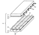
図1は、本発明の実施の形態に係るプラズマディスプレイ装置におけるプラズマディスプレイパネルの一部を示す分解斜視図である。 FIG. 1 is an exploded perspective view showing a part of a plasma display panel in a plasma display apparatus according to an embodiment of the present invention.
プラズマディスプレイパネル(以下パネルという)10は、互いに対向配置されたガラス製の前面基板21及び背面基板31を備え、前面基板21と背面基板31の間に放電空間が形成されている。
The plasma display panel (hereinafter referred to as a panel) 10 includes a glass
前面基板21には、表示電極を構成する複数対の走査電極22及び維持電極23が互いに平行に形成されている。それらの走査電極22及び維持電極23を覆うように誘電体層24が形成され、誘電体層24上には保護層25が形成されている。
On the
背面基板31には、絶縁体層33で覆われた複数のデータ電極32が設けられ、そして絶縁体層33上には井桁状の隔壁34が設けられている。また、絶縁体層33の表面及び隔壁34の側面に蛍光体層35が設けられている。
A plurality of
そして、複数対の走査電極22及び維持電極23と複数のデータ電極32とが直交するように前面基板21と背面基板31とが対向配置され、前面基板21と背面基板31との間の放電空間には、放電ガスとして、例えばネオンとキセノンとの混合ガスが封入されている。なお、パネルの構造は上述したものに限られず、例えばストライプ状の隔壁を備えた構造を用いてもよい。
The
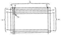
図2はパネルの電極配列図である。行方向に沿ってn本の走査電極SC1〜SCn(図1の走査電極22)及びn本の維持電極SU1〜SUn(図1の維持電極23)が配列され、列方向に沿ってm本のデータ電極D1〜Dm(図1のデータ電極32)が配列されている。そして、1対の走査電極SCi(i=1〜n)及び維持電極SUi(i=1〜n)と1つのデータ電極Dj(j=1〜m)とが交差した部分に放電セルDCが形成されている。それにより、放電空間内にm×n個の放電セルが形成されている。
FIG. 2 is an electrode array diagram of the panel. N scan electrodes SC1 to SCn (
図3は本発明の実施の形態に係るプラズマディスプレイ装置の回路ブロック図である。このプラズマディスプレイ装置は、パネル10、画像信号処理回路51、データ電極駆動回路52、複数の走査電極それぞれが接続されかつ走査電極への電圧の印加を制御する複数のドライバ回路(図示せず)を備えた走査電極駆動回路53、維持電極駆動回路54、タイミング発生回路55及び電源回路(図示せず)を備える。
FIG. 3 is a circuit block diagram of the plasma display apparatus according to the embodiment of the present invention. The plasma display device includes a
画像信号処理回路51は、画像信号sigをパネル10の画素数に応じた画像データに変換し、各画素の画像データを複数のサブフィールド(以下SFという)に対応する複数のビットに分割し、それらをデータ電極駆動回路52に出力する。
The image
データ電極駆動回路52は、SF毎の画像データを各データ電極D1〜Dmに対応する信号に変換し、その信号に基づいて各データ電極D1〜Dmを駆動する。
The data
タイミング発生回路55は、水平同期信号H及び垂直同期信号Vに基づいてタイミング信号を発生し、それらのタイミング信号をそれぞれの駆動回路ブロック(画像信号処理回路51、データ電極駆動回路52、走査電極駆動回路53及び維持電極駆動回路54)へ供給する。
The
走査電極駆動回路53は、タイミング信号に基づいて走査電極SC1〜SCnに駆動電圧波形(以下、駆動波形と略記する)を供給し、維持電極駆動回路54はタイミング信号に基づいて維持電極SU1〜SUnに駆動波形を供給する。
Scan
ここで、本実施の形態においては、走査電極SC1〜SCnについて、連続する複数の走査電極SC1,SC2,SC3,…,SCn/2を第1の走査電極群、次に連続する走査電極SCn/2+1,SCn/2+2,SCn/2+3,…,SCnを第2の走査電極群として、複数単位の走査電極群に分割しており、また走査電極駆動回路53は、第1の走査電極群に対して第1の駆動波形を供給し、第2の走査電極群に対して第2の駆動波形を供給するように構成されている。なお、以降の説明において、上記第1の走査電極群により構成される複数の放電セルを第1の放電セル群と称し、上記第2の走査電極群により構成される複数の放電セルを第1の放電セル群と称する。
Here, in the present embodiment, for scan electrodes SC1 to SCn, a plurality of continuous scan electrodes SC1, SC2, SC3,..., SCn / 2 are set as the first scan electrode group, and then the next continuous scan electrode SCn / 2 + 1, SCn / 2 + 2, SCn / 2 + 3,..., SCn are divided into a plurality of scan electrode groups as a second scan electrode group, and the scan
次に、上述の第1の駆動波形について第1の走査電極群に属する走査電極SC1を、第2の駆動波形を第2の走査電極群に属する走査電極SCn/2+1をそれぞれ例に挙げて説明する。 Next, the first drive waveform will be described by taking scan electrode SC1 belonging to the first scan electrode group as an example, and the second drive waveform will be described by taking scan electrode SCn / 2 + 1 belonging to the second scan electrode group as an example. To do.
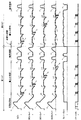
図4は、図3のプラズマディスプレイ装置のSF構成における駆動波形図である。 FIG. 4 is a drive waveform diagram in the SF configuration of the plasma display apparatus of FIG.
図4には、第1の走査電極群の1本の走査電極SC1、第2の走査電極群の1本の走査電極SCn/2+1、維持電極SU1〜SUn、及びデータ電極D1〜Dmの駆動波形を示している。なお、図4には、1フィールドのうち第1SFの初期化期間から第2SFの維持期間までが示される。 FIG. 4 shows driving waveforms of one scan electrode SC1 of the first scan electrode group, one scan electrode SCn / 2 + 1 of the second scan electrode group, sustain electrodes SU1 to SUn, and data electrodes D1 to Dm. Is shown. FIG. 4 shows from the initialization period of the first SF to the sustain period of the second SF in one field.
図4において、第1SFの初期化期間の前半部では、データ電極D1〜Dmの電位をVdaに保持し、維持電極SU1〜SUnを0V(接地電位)に保持し、走査電極SC1〜SCnにランプ波形L1を印加する。 In FIG. 4, in the first half of the initializing period of the first SF, the potentials of the data electrodes D1 to Dm are held at Vda, the sustain electrodes SU1 to SUn are held at 0 V (ground potential), and the scan electrodes SC1 to SCn are ramped. Waveform L1 is applied.
このランプ波形L1は、放電開始電圧以下の正の電位Vscnから放電開始電圧を超える正の電位(Vsus+Vset)に向かって緩やかに上昇する。すると、全ての放電セルにおいて1回目の微弱な初期化放電が起こり、走査電極SC1〜SCn上に負の壁電荷が蓄えられるとともに、維持電極SU1〜SUn上及びデータ電極D1〜Dm上に正の壁電荷が蓄えられる。ここで、電極を覆う誘電体層または蛍光体層上等に蓄積した壁電荷により生じる電圧を電極上の壁電圧という。 The ramp waveform L1 gradually rises from a positive potential Vscn equal to or lower than the discharge start voltage toward a positive potential (Vsus + Vset) exceeding the discharge start voltage. Then, the first weak initializing discharge occurs in all the discharge cells, negative wall charges are accumulated on scan electrodes SC1 to SCn, and positive on sustain electrodes SU1 to SUn and data electrodes D1 to Dm. Wall charges are stored. Here, the voltage generated by the wall charges accumulated on the dielectric layer or the phosphor layer covering the electrode is referred to as the wall voltage on the electrode.
続く初期化期間の後半部では、データ電極D1〜Dmを接地電位に保持し、維持電極SU1〜SUnを正の電位Ve1に保持し、第1の走査電極群(走査電極SC1〜SCn/2)に正の電位(Vsus)から負の電位(−Vad+Vset2)に向かって緩やかに下降するランプ波形L2を印加する。すると第1の放電セル群において2回目の微弱な初期化放電が起こる。これにより、走査電極SCi上の壁電圧及び維持電極SUi上の壁電圧が弱められ、データ電極Dj上の壁電圧も書込み動作に適した値に調整される。 In the latter half of the subsequent initialization period, the data electrodes D1 to Dm are held at the ground potential, the sustain electrodes SU1 to SUn are held at the positive potential Ve1, and the first scan electrode group (scan electrodes SC1 to SCn / 2) A ramp waveform L2 that gently falls from a positive potential (Vsus) to a negative potential (−Vad + Vset2) is applied. Then, a second weak setup discharge occurs in the first discharge cell group. Thereby, the wall voltage on scan electrode SCi and the wall voltage on sustain electrode SUi are weakened, and the wall voltage on data electrode Dj is also adjusted to a value suitable for the write operation.
一方、第2の走査電極群(走査電極SCn/2+1〜SCn)には、正の電位(Vsus)から負の電位(−Vad+Vhiz)に向かって緩やかに下降するランプ波形L3を印加する。ここで、初期化期間の後半部において第2の走査電極群に印加されるランプ波形L3は、第1の走査電極群に印加されるランプ波形L2よりも高い電圧に緩やかに向かって下降する。それにより、第2の放電セル群においては、書込み動作に適した壁電荷に調整される前に2回目の初期化放電が終了する。 On the other hand, the ramp waveform L3 that gently falls from the positive potential (Vsus) toward the negative potential (−Vad + Vhiz) is applied to the second scan electrode group (scan electrodes SCn / 2 + 1 to SCn). Here, the ramp waveform L3 applied to the second scan electrode group in the second half of the initialization period gradually decreases toward a voltage higher than the ramp waveform L2 applied to the first scan electrode group. Thereby, in the second discharge cell group, the second initializing discharge is completed before the wall charge is adjusted to be suitable for the address operation.
第1SFの書込み期間の前半部では、維持電極SU1〜SUnを一旦電位Ve2に保持し、走査電極SC1〜SCnを一旦電位(−Vad+Vscn)に保持する。ここで、まず第1の走査電極群の書込み動作について説明する。 In the first half of the address period of the first SF, sustain electrodes SU1 to SUn are temporarily held at potential Ve2, and scan electrodes SC1 to SCn are temporarily held at potential (−Vad + Vscn). Here, the address operation of the first scan electrode group will be described first.
1行目の走査電極SC1に負の走査パルスPa(=−Vad)を印加するとともに、データ電極D1〜Dmのうち1行目において発光すべき放電セルのデータ電極Dk(kは1〜mのいずれか)に正の書込みパルスPd(=Vda)を印加する。すると、データ電極Dkと走査電極SC1との交差部の電圧は、外部印加電圧(Pd−Pa)にデータ電極Dk上の壁電圧及び走査電極SC1上の壁電圧が加算された値となり、放電開始電圧を超える。それにより、データ電極Dkと走査電極SC1との間及び維持電極SU1と走査電極SC1との間で書込み放電が発生する。その結果、その放電セルの走査電極SC1上に正の壁電荷が蓄積され、維持電極SU1上に負の壁電荷が蓄積され、データ電極Dk上にも負の壁電荷が蓄積される。 The negative scan pulse Pa (= −Vad) is applied to the scan electrode SC1 in the first row, and the data electrode Dk (k is 1 to m of the discharge cell) to emit light in the first row among the data electrodes D1 to Dm. A positive write pulse Pd (= Vda) is applied to any one of them. Then, the voltage at the intersection of the data electrode Dk and the scan electrode SC1 becomes a value obtained by adding the wall voltage on the data electrode Dk and the wall voltage on the scan electrode SC1 to the externally applied voltage (Pd-Pa), and the discharge starts. Over voltage. Thereby, address discharge is generated between data electrode Dk and scan electrode SC1, and between sustain electrode SU1 and scan electrode SC1. As a result, positive wall charges are accumulated on scan electrode SC1 of the discharge cell, negative wall charges are accumulated on sustain electrode SU1, and negative wall charges are also accumulated on data electrode Dk.
このようにして、1行目において発光すべき放電セルで書込み放電が発生して各電極上に壁電荷を蓄積させる書込み動作が行われる。一方、書込みパルスPdが印加されなかったデータ電極Dh(h≠k)と走査電極SC1との交差部の電圧は放電開始電圧を超えないので、書込み放電は発生しない。 In this manner, the address operation is performed in which the address discharge is generated in the discharge cells to emit light in the first row and the wall charges are accumulated on the respective electrodes. On the other hand, the voltage at the intersection between the data electrode Dh (h ≠ k) to which the address pulse Pd is not applied and the scan electrode SC1 does not exceed the discharge start voltage, so that address discharge does not occur.
上記走査電極SC1の書込み動作後、続く第1の走査電極群に属する奇数ラインの走査電極SC3、SC5、…、SCn/2−1まで上記書込み動作を順次行った後、第1の走査電極群に属する偶数ラインの走査電極SC2、SC4、…、SCn/2までの上記書込み動作を順次行い、第1の放電セル群の書込み動作が完了する。 After the address operation of scan electrode SC1, the address operation is sequentially performed up to scan electrodes SC3, SC5,..., SCn / 2-1 of odd lines belonging to the subsequent first scan electrode group, and then the first scan electrode group , SCn / 2 are sequentially performed for the even-numbered scan electrodes SC2, SC4,..., SCn / 2, and the address operation of the first discharge cell group is completed.
なお、第1の走査電極群の書込み期間の後半では、維持電極SU1〜SUnが電位Ve1に保持され、全ての走査電極SC1〜SCnに接地電位から負の電位(−Vad+Vset2)に向かって緩やかに下降するランプ波形L4が印加されるが、これは以降で詳述する第2の走査電極群の初期化動作に伴うものであり、第1の走査電極群の書込み動作に影響を与えない。 In the second half of the address period of the first scan electrode group, sustain electrodes SU1 to SUn are held at potential Ve1, and all scan electrodes SC1 to SCn are gradually increased from the ground potential toward a negative potential (−Vad + Vset2). The descending ramp waveform L4 is applied, which is accompanied by the initialization operation of the second scan electrode group, which will be described in detail later, and does not affect the write operation of the first scan electrode group.
ここで、第1の走査電極群に走査パルスPaが印加される期間には、第2の走査電極群には走査パルスPaが印加されない。この期間において、第2の放電セル群の壁電荷は減少する。しかしながら、上述したように、第2の放電セル群においては初期化期間において2回目の微弱な初期化放電が書込み動作に適した壁電荷になる前に停止している。そのため、初期化期間が終了した時点においては、第2の放電セル群には第1の放電セル群より十分多い壁電荷が保持されている。したがって、上記の期間において、第2の放電セル群の壁電荷が減少しても、第2の放電セル群にはまだ十分な量の壁電荷が保持されている。 Here, during the period in which the scan pulse Pa is applied to the first scan electrode group, the scan pulse Pa is not applied to the second scan electrode group. During this period, the wall charge of the second discharge cell group decreases. However, as described above, in the second discharge cell group, the second weak setup discharge is stopped in the setup period before the wall charge suitable for the address operation is reached. Therefore, at the end of the initialization period, the second discharge cell group holds a sufficiently larger amount of wall charges than the first discharge cell group. Therefore, even if the wall charge of the second discharge cell group decreases during the above period, a sufficient amount of wall charge is still held in the second discharge cell group.
そこで、本実施の形態においては、第2の走査電極群に走査パルスPaを印加する直前に、走査電極SC1〜SCnに接地電位から負の電位(−Vad+Vset2)に向かって緩やかに下降するランプ波形L4を印加する。すると、第2の放電セル群において2回目の微弱な初期化放電の続きとも言える第3の初期化放電が起こる。これにより、第2の放電セル群において、走査電極SCi上の壁電圧及び維持電極SUiの壁電圧が弱められ、データ電極Dk上の壁電圧も書込み動作に適した値に調整される。 Therefore, in the present embodiment, immediately before the scan pulse Pa is applied to the second scan electrode group, the ramp waveform gently falls from the ground potential toward the negative potential (−Vad + Vset2) to the scan electrodes SC1 to SCn. L4 is applied. Then, a third initializing discharge that can be said to be a continuation of the second weak initializing discharge occurs in the second discharge cell group. Thereby, in the second discharge cell group, the wall voltage on scan electrode SCi and the wall voltage on sustain electrode SUi are weakened, and the wall voltage on data electrode Dk is also adjusted to a value suitable for the address operation.
すなわち、本実施の形態においては、第1SFの初期化期間において第1の放電セル群に属する全ての放電セルの初期化動作(第1の放電セル群の全セル初期化動作)が行われ、第1SFの初期化期間及び書込み期間において第2の放電セル群に属する全ての放電セルの初期化動作(第2の放電セル群の全セル初期化動作)が行われることとなる。 That is, in the present embodiment, the initialization operation of all discharge cells belonging to the first discharge cell group (all cell initialization operation of the first discharge cell group) is performed in the initialization period of the first SF, In the initialization period and address period of the first SF, the initialization operation of all discharge cells belonging to the second discharge cell group (all cell initialization operation of the second discharge cell group) is performed.
次に第2の放電セル群の書込み動作について説明する。 Next, the address operation of the second discharge cell group will be described.
第1SFの書込み期間の後半部(上記ランプ波形L4の印加後)では、維持電極SU1〜SUnを再び電位Ve2に保持し、走査電極SC1〜SCnを一旦電位(−Vad+Vscn)に保持する。次に、第2の走査電極群の奇数ラインであるn/2+1行目の走査電極SCn/2+1に負の走査パルスPaを印加するとともに、データ電極D1〜Dmのうちn/2+1行目において発光すべき放電セルのデータ電極Dkに正の書込みパルスPdを印加する。すると、データ電極Dkと走査電極SCn/2+1との交差部の電圧は、放電開始電圧を超える。それにより、データ電極Dkと走査電極SCn/2+1との間及び維持電極SUn/2+1と走査電極SCn/2+1との間で書込み放電が発生する。その放電セルの走査電極SCn/2+1上に正の壁電荷が蓄積され、維持電極SCn/2+1上に負の壁電荷が蓄積され、データ電極Dk上にも負の壁電荷が蓄積される。 In the second half of the address period of the first SF (after application of the ramp waveform L4), the sustain electrodes SU1 to SUn are held again at the potential Ve2, and the scan electrodes SC1 to SCn are once held at the potential (−Vad + Vscn). Next, a negative scan pulse Pa is applied to the scan electrode SCn / 2 + 1 in the n / 2 + 1 row, which is an odd line of the second scan electrode group, and light is emitted in the n / 2 + 1 row among the data electrodes D1 to Dm. A positive address pulse Pd is applied to the data electrode Dk of the discharge cell to be discharged. Then, the voltage at the intersection of data electrode Dk and scan electrode SCn / 2 + 1 exceeds the discharge start voltage. Thereby, an address discharge is generated between data electrode Dk and scan electrode SCn / 2 + 1 and between sustain electrode SUn / 2 + 1 and scan electrode SCn / 2 + 1. Positive wall charges are accumulated on scan electrode SCn / 2 + 1 of the discharge cell, negative wall charges are accumulated on sustain electrode SCn / 2 + 1, and negative wall charges are also accumulated on data electrode Dk.
このようにして、n/2+1行目において発光すべき放電セルで書込み放電が発生して各電極上に壁電荷を蓄積させる書込み動作が行われる。一方、書込みパルスPdが印加されなかったデータ電極Dhと走査電極SCn/2+1との交差部の電圧は放電開始電圧を超えないので、書込み放電は発生しない。 In this manner, an address operation is performed in which address discharge occurs in the discharge cells to emit light in the n / 2 + 1th row and wall charges are accumulated on each electrode. On the other hand, the voltage at the intersection between the data electrode Dh to which the address pulse Pd is not applied and the scan electrode SCn / 2 + 1 does not exceed the discharge start voltage, so that address discharge does not occur.
上記SCn/2+1の書込み動作後、続く第2走査電極群に属する奇数ラインの走査電極SCn/2+3、SCn/2+5、…、SCn−1まで上記書込み動作を順次行った後、第2走査電極群に属する偶数ラインの走査電極SCn/2+2、SCn/2+4、…、SCnまでの上記書込み動作を順次行い、第2の放電セル群の書込み動作が完了する。 After the SCn / 2 + 1 address operation, the address operation is sequentially performed up to the scan electrodes SCn / 2 + 3, SCn / 2 + 5,..., SCn−1 of the odd lines belonging to the subsequent second scan electrode group, and then the second scan electrode group , SCn of the even-numbered scan electrodes SCn / 2 + 4,..., SCn are sequentially performed, and the address operation of the second discharge cell group is completed.
続く維持期間では、維持電極SU1〜SUnを接地電位に戻し、走査電極SC1〜SCnに維持期間の最初の維持パルスPs(=Vsus)を印加する。このとき、書込み期間で書込み放電が発生した放電セルにおいては、走査電極SCiと維持電極SUiとの間の電圧は、維持パルスPsに走査電極SCi上の壁電圧及び維持電極SUi上の壁電圧が加算された値となり、放電開始電圧を超える。それにより、走査電極SCiと維持電極SUiとの間で維持放電が起こり、放電セルが発光する。その結果、走査電極SCi上に負の壁電荷が蓄積され、維持電極SUi上に正の壁電荷が蓄積され、データ電極Dk上に正の壁電荷が蓄積される。 In the subsequent sustain period, sustain electrodes SU1 to SUn are returned to the ground potential, and first sustain pulse Ps (= Vsus) in the sustain period is applied to scan electrodes SC1 to SCn. At this time, in a discharge cell in which an address discharge has occurred in the address period, the voltage between scan electrode SCi and sustain electrode SUi is such that the wall voltage on scan electrode SCi and the wall voltage on sustain electrode SUi are included in sustain pulse Ps. The added value exceeds the discharge start voltage. Accordingly, a sustain discharge occurs between scan electrode SCi and sustain electrode SUi, and the discharge cell emits light. As a result, negative wall charges are accumulated on scan electrode SCi, positive wall charges are accumulated on sustain electrode SUi, and positive wall charges are accumulated on data electrode Dk.
以降同様に、走査電極SC1〜SCnと維持電極SU1〜SUnとにあらかじめ定められた数の維持パルスPsを交互に印加することにより、書込み期間において書込み放電が発生した放電セルでは維持放電が継続して行われる。 Similarly, sustain discharge continues in the discharge cells in which the address discharge has occurred in the address period by alternately applying a predetermined number of sustain pulses Ps to scan electrodes SC1 to SCn and sustain electrodes SU1 to SUn. Done.
維持パルスPsの印加後、維持電極SUi及びデータ電極Dkを接地電位に保持した状態で、走査電極SCiにランプ波形L5を印加する。このランプ波形L5は、接地電位からの正の電位Veraseに向かって緩やかに上昇する。これにより、維持放電が起こった放電セルにおいて、走査電極SCiと維持電極SUiとの間の電圧が放電開始電圧を超え、維持電極SUiと走査電極SCiとの間で微弱な消去放電が発生する。 After the sustain pulse Ps is applied, the ramp waveform L5 is applied to the scan electrode SCi with the sustain electrode SUi and the data electrode Dk held at the ground potential. The ramp waveform L5 gradually rises from the ground potential toward the positive potential Verase. As a result, in the discharge cell in which the sustain discharge has occurred, the voltage between scan electrode SCi and sustain electrode SUi exceeds the discharge start voltage, and a weak erasure discharge occurs between sustain electrode SUi and scan electrode SCi.
その結果、走査電極SCiに負の壁電荷が蓄積され、維持電極SUiに正の壁電荷が蓄積される。このとき、データ電極Dk上には正の壁電荷が蓄積される。その後、走査電極SCiを接地電位に戻し、維持期間における維持動作を終了する。 As a result, negative wall charges are accumulated on scan electrode SCi, and positive wall charges are accumulated on sustain electrode SUi. At this time, positive wall charges are accumulated on the data electrode Dk. Thereafter, scan electrode SCi is returned to the ground potential, and the sustain operation in the sustain period is terminated.
第2SFの初期化期間では、維持電極SU1〜SUnを電位Ve1に保持し、データ電極D1〜Dmを接地電位に保持し、第1の走査電極群(走査電極SC1,SC2,…,SCn/2)に接地電位からの負の電位(−Vad+Vset3)に向かって緩やかに下降するランプ波形L6を印加する。すると、第1の放電セル群のうち、前のSFで(図4では第1SF)の維持期間で維持放電が起こった放電セルでは微弱な初期化放電が発生する。それにより、第1の放電セル群のうち前のSFで維持放電が起こった放電セルにおいて、走査電極SCi上の壁電圧及び維持電極SUi上の壁電圧が弱められ、データ電極Dk上の壁電圧も書込み動作に適した値に調整される。 In the initialization period of the second SF, sustain electrodes SU1 to SUn are held at potential Ve1, data electrodes D1 to Dm are held at ground potential, and the first scan electrode group (scan electrodes SC1, SC2,..., SCn / 2). ) Is applied with a ramp waveform L6 that gradually falls toward a negative potential (−Vad + Vset3) from the ground potential. Then, in the first discharge cell group, a weak initializing discharge is generated in the discharge cell in which the sustain discharge has occurred in the sustain period of the previous SF (first SF in FIG. 4). As a result, the wall voltage on the scan electrode SCi and the wall voltage on the sustain electrode SUi are weakened in the discharge cells in which the sustain discharge has occurred in the previous SF in the first discharge cell group, and the wall voltage on the data electrode Dk. Is also adjusted to a value suitable for the write operation.
前のSFで維持放電が起こらなかった放電セルにおいては、放電が発生することはなく、前のSFの初期化期間の終了時における壁電荷の状態がそのままに保たれる。 In a discharge cell in which no sustain discharge has occurred in the previous SF, no discharge occurs, and the state of the wall charge at the end of the initialization period of the previous SF is maintained as it is.
一方、第2の走査電極群(走査電極SCn/2+1,SCn/2+2,…,SCn)には、接地電位からの負の電位(−Vad+Vhiz)に向かって緩やかに下降するランプ波形L7を印加する。このとき、第2の放電セル群のうち前のSFで維持放電が起こった放電セルでは微弱な初期化放電が発生するが、第1の走査電極群に印加されるランプ波形L6よりも高い電圧に緩やかに向かって下降するため、第2の放電セル群においては、書込み動作に適した壁電荷に調整される前にランプ波形L7による初期化放電が終了する。
前のSFで維持放電が起こらなかった放電セルにおいては、放電が発生することはなく、前のSFの初期化期間の終了時における壁電荷の状態がそのままに保たれる。
On the other hand, a ramp waveform L7 that gently falls toward the negative potential (−Vad + Vhiz) from the ground potential is applied to the second scan electrode group (scan electrodes SCn / 2 + 1, SCn / 2 + 2,..., SCn). . At this time, a weak initializing discharge occurs in the discharge cells in which the sustain discharge has occurred in the previous SF in the second discharge cell group, but the voltage is higher than the ramp waveform L6 applied to the first scan electrode group. Therefore, in the second discharge cell group, the initializing discharge by the ramp waveform L7 is completed before the wall charge suitable for the address operation is adjusted.
In the discharge cell in which no sustain discharge has occurred in the previous SF, no discharge occurs, and the state of the wall charge at the end of the initialization period of the previous SF is maintained as it is.
したがって、第2の放電セル群に蓄積されている壁電荷の量は、第1の放電セル群に蓄積されている壁電荷の量に比べて十分に多い。 Therefore, the amount of wall charges accumulated in the second discharge cell group is sufficiently larger than the amount of wall charges accumulated in the first discharge cell group.
第2SFの書込み期間においては、維持電極SU1〜SUn及びデータ電極D1〜Dmに対して第1SFの書込み期間と同様の駆動波形を供給する。 In the second SF address period, the drive waveforms similar to those in the first SF address period are supplied to the sustain electrodes SU1 to SUn and the data electrodes D1 to Dm.
この場合、第1SFと同様に、第2SFの書込み期間において第1の走査電極群に走査パルスPaが印加される期間には、第2の走査電極群には走査パルスPaが印加されない。この期間において、第2の放電セル群の壁電荷は減少する。しかしながら、上述したように、第2の放電セル群には第2SFの初期化期間終了時に十分な量の壁電荷が保持されている。従って上記の期間においてそれらの放電セルの壁電荷が減少しても、それらの放電セルにはまだ十分な量の壁電荷が保持されている。 In this case, similarly to the first SF, the scan pulse Pa is not applied to the second scan electrode group during the period in which the scan pulse Pa is applied to the first scan electrode group in the writing period of the second SF. During this period, the wall charge of the second discharge cell group decreases. However, as described above, a sufficient amount of wall charges are held in the second discharge cell group at the end of the initialization period of the second SF. Therefore, even if the wall charges of the discharge cells are reduced during the above period, a sufficient amount of wall charges is still held in the discharge cells.
そこで、第2の走査電極群に走査パルスPaを印加する直前に、走査電極SC1〜SCnに接地電位から負の電位(−Vad+Vset4)に向かって緩やかに下降するランプ波形L8を印加する。すると、第2の放電セル群のうち前のSFで維持放電が起こった放電セルにおいてランプ波形L7の微弱な初期化放電の続きとも言える初期化放電が起こる。これにより、第2の放電セルのうち前のSFで維持放電が起こった放電セルにおいて、走査電極SCi上の壁電圧及び維持電極SUiの壁電圧が弱められ、データ電極Dk上の壁電圧も書込み動作に適した値に調整される。 Therefore, immediately before the scan pulse Pa is applied to the second scan electrode group, the ramp waveform L8 that gently falls from the ground potential toward the negative potential (−Vad + Vset4) is applied to the scan electrodes SC1 to SCn. Then, an initializing discharge that can be said to be a continuation of the weak initializing discharge of the ramp waveform L7 occurs in the discharge cells in which the sustain discharge has occurred in the previous SF in the second discharge cell group. As a result, in the discharge cells in which the sustain discharge has occurred in the previous SF among the second discharge cells, the wall voltage on the scan electrode SCi and the wall voltage on the sustain electrode SUi are weakened, and the wall voltage on the data electrode Dk is also written. It is adjusted to a value suitable for operation.
また、第2SFにおける書込み動作を行う順序も第1SFと同様の順序となる。 Further, the order of performing the write operation in the second SF is the same order as in the first SF.
つまり、第1の走査電極群における奇数ラインの書込み動作を行い、次いで偶数ラインの書込み動作を行う。第1の走査電極群の書込み動作が完了した後、順次第2の走査電極群における奇数ラインの書込み動作を行い、次いで偶数ラインの書込み動作を行い、第2SFの書込み期間を終える。 That is, an odd line write operation is performed in the first scan electrode group, and then an even line write operation is performed. After the write operation of the first scan electrode group is completed, the odd line write operation in the second scan electrode group is sequentially performed, then the even line write operation is performed, and the second SF write period ends.
なお、第2SFの維持期間においては、第1SFの維持期間と同様に、走査電極SC1〜SCnと維持電極SU1〜SUnとにあらかじめ定められら数の維持パルスPsを交互に印加する。それにより、書込み期間において書込み放電が発生した放電セルで維持放電が行われる。 In the sustain period of the second SF, similarly to the sustain period of the first SF, a predetermined number of sustain pulses Ps are alternately applied to scan electrodes SC1 to SCn and sustain electrodes SU1 to SUn. Thereby, the sustain discharge is performed in the discharge cells in which the address discharge has occurred in the address period.
また、第3SF以降のSFでは、第1の走査電極群、第2の走査電極群、維持電極SU1〜SUn及びデータ電極D1〜Dmに対して第2SFと同様の駆動波形を供給する。 In SF after the third SF, the same drive waveform as that of the second SF is supplied to the first scan electrode group, the second scan electrode group, the sustain electrodes SU1 to SUn, and the data electrodes D1 to Dm.
また、書込み動作を行う順序においても、第1SF及び第2SFと同様の順序となる。つまり、第1の走査電極群における奇数ラインの書込み動作を行い、次いで偶数ラインの書込み動作を行う。第1の走査電極群の書込み動作が完了した後、第2の走査電極群における奇数ラインの書込み動作を行い、次いで偶数ラインの書込み動作を行い、そのSFの書込み期間を終える。 Also, the order in which the write operation is performed is the same order as the first SF and the second SF. That is, an odd line write operation is performed in the first scan electrode group, and then an even line write operation is performed. After the write operation of the first scan electrode group is completed, the odd line write operation in the second scan electrode group is performed, then the even line write operation is performed, and the SF write period ends.
以上のように、本発明においては、連続する複数の走査電極群を1単位として、第1の走査電極群、第2の走査電極群のように複数単位の走査電極群に分割し、そして各単位の第1の走査電極群、第2の走査電極群は、走査電極に初期化パルスを印加して初期化動作を行い、その後走査電極の奇数ラインまたは偶数ラインのうち一方のラインの書込み動作を行った後、他方のラインの書込み動作を行うように構成し、かつ第1の走査電極群、第2の走査電極群単位に順次初期化動作及び書込み動作を行うように構成したものである。このような構成により、第1の走査電極群に分類された連続する複数の走査電極は、隣接する走査電極間で全て同様の駆動波形となり、また第2の走査電極群に分類された連続する複数の走査電極も、隣接する走査電極間で同様の駆動波形となり、走査電極駆動回路の構成が複雑化することがない。 As described above, in the present invention, a plurality of continuous scan electrode groups are taken as one unit, and divided into a plurality of units of scan electrode groups such as the first scan electrode group and the second scan electrode group, The first scan electrode group and the second scan electrode group of the unit perform an initialization operation by applying an initialization pulse to the scan electrodes, and then write operation of one of the odd lines or even lines of the scan electrodes After performing the above, the other line is subjected to the write operation, and the initial scan operation and the write operation are sequentially performed in units of the first scan electrode group and the second scan electrode group. . With such a configuration, a plurality of continuous scan electrodes classified into the first scan electrode group all have the same drive waveform between adjacent scan electrodes, and are consecutively classified into the second scan electrode group. The plurality of scan electrodes also have the same drive waveform between adjacent scan electrodes, and the configuration of the scan electrode drive circuit is not complicated.
また、上述したように、書込み動作が行われる順番が早い第1の走査電極群は、通常通り初期化放電を経て書込み動作を順次行い、そして書込み動作が行われる順番が遅い第2の走査電極群は、書込み動作が行われる直前に初期化放電を別途行うように構成する、すなわち走査電極を書込み動作が行われる順番により分割し、初期化放電を行うタイミングが異なる駆動波形を印加することにより、走査パルスが印加される順番が遅い走査電極群においても、初期化放電を行ってから壁電荷が減少する時間が短くなるため、書込み放電不良が発生するのを防止することができる。 Further, as described above, the first scan electrode group in which the address operation is performed in the first order performs the address operation sequentially through the initializing discharge as usual, and the second scan electrode in which the address operation is performed in the later order. The group is configured to perform initializing discharge separately immediately before the addressing operation is performed, that is, by dividing the scan electrodes according to the order in which the addressing operation is performed, and applying drive waveforms having different timings for performing the initializing discharge. Even in the scan electrode group in which the scan pulse is applied in a slow order, the time for the wall charge to decrease after performing the initializing discharge is shortened, so that it is possible to prevent the address discharge failure from occurring.
さらに、プラズマディスプレイ装置の書込み期間での書込み電力の大部分を占める、変位電流による消費電力は下記の数式で示される。 Furthermore, the power consumption due to the displacement current, which occupies most of the writing power in the writing period of the plasma display device, is expressed by the following mathematical formula.
P=IV=CV2f
ここで、Iは電流、Vはデータ電極に印加されるデータパルスの電圧、Cは隣接する電極との間の静電容量、fは周波数で、パネルのデータ電極への電圧印加を制御するデータドライバーの半導体装置(IC)の単位時間当たりの平均スイッチング回数である。
P = IV = CV 2 f
Here, I is a current, V is a voltage of a data pulse applied to the data electrode, C is a capacitance between adjacent electrodes, f is a frequency, and data for controlling voltage application to the data electrode of the panel This is the average number of switching times per unit time of the driver's semiconductor device (IC).
上記数式に示されるように、データドライバーのスイッチング回数を減らすことで書込み電力を低減することができる。 As shown in the above formula, the write power can be reduced by reducing the number of times the data driver is switched.
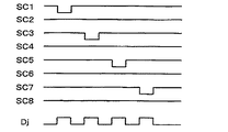
ところで、図5に示す表示パターンについて、走査電極SC1からSCnへ順次書込み動作を行うと、1フィールド期間を分割したうちの1つのSFにおけるデータパルスのパターンは図6に示すようになり、データパルスのON/OFFが繰り返されるため、データドライバーのスイッチング回数が多くなる。これにより消費電力は大きくなり、またデータドライバーの発熱量も大きくなる。 By the way, for the display pattern shown in FIG. 5, when the address operation is sequentially performed from scan electrodes SC1 to SCn, the data pulse pattern in one SF of one field period is as shown in FIG. Since the ON / OFF operation is repeated, the number of times the data driver is switched increases. As a result, power consumption increases and the amount of heat generated by the data driver also increases.
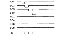
これに対し、本発明においては、図5に示す表示パターンについて、走査電極を奇数ラインと偶数ラインとに分割し、偶数ラインまたは奇数ラインのうち一方のみに順次書込み動作を行った後、他方のラインの書込み動作を順次行う、いわゆる飛び越し走査における1フィールド期間を分割したうちの1つのSFにおけるデータパルスのパターンは図7に示すようになり、飛び越し走査によりデータパルスのON/OFFの繰り返しはなく、ONもしくはOFFの状態が続き、データドライバーのスイッチング回数が低減され、書込み電力を抑制することができる。 On the other hand, in the present invention, for the display pattern shown in FIG. 5, the scan electrode is divided into odd lines and even lines, and after the sequential write operation is performed on only one of the even lines or odd lines, the other is performed. The pattern of data pulses in one SF in which one field period in so-called interlaced scanning in which line writing operations are sequentially performed is as shown in FIG. 7, and there is no repetition of ON / OFF of data pulses by interlaced scanning. , The ON or OFF state continues, the number of times the data driver is switched is reduced, and the write power can be suppressed.
次に、本発明の他の実施の形態による駆動方法について、図8に示す駆動波形図を用いて説明する。なお、パネルの構成、パネルの電極配列、回路ブロックの構成は、図1〜図3に示したものと同様である。 Next, a driving method according to another embodiment of the present invention will be described with reference to a driving waveform diagram shown in FIG. The panel configuration, the panel electrode arrangement, and the circuit block configuration are the same as those shown in FIGS.
本実施の形態においては、走査電極SC1〜SCnについて、走査電極SC1,SC2,SC3,…,SCn/3を第1の走査電極群、走査電極SCn/3+1,SCn/3+2,SCn/3+3,…,SC2n/3を第2の走査電極群、走査電極SC2n/3+1,SC2n/3+2,SC2n/3+3,…,SCnを第3の走査電極群として分割し、走査電極駆動回路53は、第1の走査電極群に対して第1の駆動波形を供給し、第2の走査電極群に対して第2の駆動波形を供給し、第3の走査電極群に対して第3の駆動波形を供給するように構成している。また、上記第1の走査電極群により構成される複数の放電セルを第1の放電セル群と称し、上記第2の走査電極群により構成される複数の放電セルを第2の放電セル群と称し、上記第3の走査電極群により構成される複数の放電セルを第3の放電セル群と称する。 In this embodiment, for scan electrodes SC1 to SCn, scan electrodes SC1, SC2, SC3,..., SCn / 3 are replaced with the first scan electrode group, scan electrodes SCn / 3 + 1, SCn / 3 + 2, SCn / 3 + 3,. , SC2n / 3 is divided into a second scan electrode group, scan electrodes SC2n / 3 + 1, SC2n / 3 + 2, SC2n / 3 + 3,..., SCn as a third scan electrode group. A first drive waveform is supplied to the scan electrode group, a second drive waveform is supplied to the second scan electrode group, and a third drive waveform is supplied to the third scan electrode group. It is configured as follows. The plurality of discharge cells configured by the first scan electrode group are referred to as a first discharge cell group, and the plurality of discharge cells configured by the second scan electrode group are referred to as a second discharge cell group. A plurality of discharge cells constituted by the third scan electrode group is referred to as a third discharge cell group.
図8においては、第1の走査電極群の1本の走査電極SC1、第2の走査電極群の1本の走査電極SCn/3+1、第3の走査電極群の1本の走査電極SC2n/3+1、維持電極SU1〜SUn、及びデータ電極D1〜Dmの駆動波形を示している。なお、図8には、1フィールドの第1SFの初期化期間から第2SFの維持期間までを示している。 In FIG. 8, one scan electrode SC1 of the first scan electrode group, one scan electrode SCn / 3 + 1 of the second scan electrode group, and one scan electrode SC2n / 3 + 1 of the third scan electrode group. , Driving waveforms of the sustain electrodes SU1 to SUn and the data electrodes D1 to Dm are shown. FIG. 8 shows from the initializing period of the first SF of one field to the sustaining period of the second SF.
第1SFの初期化期間の前半部では、データ電極D1〜Dmの電位をVdaに保持し、維持電極SU1〜SUnを0V(接地電位)に保持し、走査電極SC1〜SCnにランプ波形L1を印加する。 In the first half of the initializing period of the first SF, the potentials of the data electrodes D1 to Dm are held at Vda, the sustain electrodes SU1 to SUn are held at 0 V (ground potential), and the ramp waveform L1 is applied to the scan electrodes SC1 to SCn. To do.
このランプ波形L1は、放電開始電圧以下の正の電位Vscnから放電開始電圧を超える正の電位(Vsus+Vset)に向かって緩やかに上昇する。すると、全ての放電セルにおいて1回目の微弱な初期化放電が起こり、走査電極SC1〜SCn上に負の壁電荷が蓄えられるとともに維持電極SU1〜SUn上及びデータ電極D1〜Dm上に正の壁電荷が蓄えられる。ここで、電極を覆う誘電体層または蛍光体層上等に蓄積した壁電荷により生じる電圧を電極上の壁電圧という。 The ramp waveform L1 gradually rises from a positive potential Vscn equal to or lower than the discharge start voltage toward a positive potential (Vsus + Vset) exceeding the discharge start voltage. Then, the first weak initializing discharge occurs in all the discharge cells, negative wall charges are stored on scan electrodes SC1 to SCn, and positive walls on sustain electrodes SU1 to SUn and data electrodes D1 to Dm. Charge is stored. Here, the voltage generated by the wall charges accumulated on the dielectric layer or the phosphor layer covering the electrode is referred to as the wall voltage on the electrode.
続く初期化期間の後半部では、データ電極D1〜Dmを接地電位に保持し、維持電極SU1〜SUnを正の電位Ve1に保持し、第1の走査電極群(走査電極SC1〜SCn/3)に正の電位(Vsus)から負の電位(−Vad+Vset2)に向かって緩やかに下降するランプ波形L2を印加する。すると第1の放電セル群において2回目の微弱な初期化放電が起こる。これにより、走査電極SCi上の壁電圧及び維持電極SUi上の壁電圧が弱められ、データ電極Dj上の壁電圧も書込み動作に適した値に調整される。 In the latter half of the subsequent initialization period, the data electrodes D1 to Dm are held at the ground potential, the sustain electrodes SU1 to SUn are held at the positive potential Ve1, and the first scan electrode group (scan electrodes SC1 to SCn / 3) A ramp waveform L2 that gently falls from a positive potential (Vsus) to a negative potential (−Vad + Vset2) is applied. Then, a second weak setup discharge occurs in the first discharge cell group. Thereby, the wall voltage on scan electrode SCi and the wall voltage on sustain electrode SUi are weakened, and the wall voltage on data electrode Dj is also adjusted to a value suitable for the write operation.
一方、第2の走査電極群(走査電極SCn/3+1〜SC2n/3)及び第3の走査電極群(走査電極SC2n/3+1〜SCn)には、正の電位(Vsus)から負の電位(−Vad+Vhiz)に向かって緩やかに下降するランプ波形L3を印加する。 On the other hand, the second scan electrode group (scan electrodes SCn / 3 + 1 to SC2n / 3) and the third scan electrode group (scan electrodes SC2n / 3 + 1 to SCn) are changed from a positive potential (Vsus) to a negative potential (− A ramp waveform L3 that gently falls toward (Vad + Vhiz) is applied.
ここで、初期化期間の後半部において第2の走査電極群及び第3の走査電極群に印加されるランプ波形L3は、第1の走査電極群に印加されるランプ波形L2よりも高い電圧に緩やかに向かって下降する。それにより、第2の放電セル群及び第3の放電セル群においては、書込み動作に適した壁電荷に調整される前に2回目の初期化放電が終了する。 Here, the ramp waveform L3 applied to the second scan electrode group and the third scan electrode group in the latter half of the initialization period is set to a voltage higher than the ramp waveform L2 applied to the first scan electrode group. It descends slowly. Thereby, in the second discharge cell group and the third discharge cell group, the second initializing discharge is completed before the wall charges are adjusted to be suitable for the address operation.
第1SFの書込み期間の前部では、維持電極SU1〜SUnを一旦電位Ve2に保持し、走査電極SC1〜SCnを一旦電位(−Vad+Vscn)に保持する。 In the front part of the address period of the first SF, sustain electrodes SU1 to SUn are temporarily held at potential Ve2, and scan electrodes SC1 to SCn are temporarily held at potential (−Vad + Vscn).
ここで、まず第1の走査電極群の書込み動作について説明する。 Here, the address operation of the first scan electrode group will be described first.
1行目の走査電極SC1に負の走査パルスPa(=−Vad)を印加するとともに、データ電極D1〜Dmのうち1行目において発光すべき放電セルのデータ電極Dk(kは1〜mのいずれか)に正の書込みパルスPd(=Vda)を印加する。すると、データ電極Dkと走査電極SC1との交差部の電圧は、外部印加電圧(Pd−Pa)にデータ電極Dk上の壁電圧及び走査電極SC1上の壁電圧が加算された値となり、放電開始電圧を超える。それにより、データ電極Dkと走査電極SC1との間及び維持電極SU1と走査電極SC1との間で書込み放電が発生する。その結果、その放電セルの走査電極SC1上に正の壁電荷が蓄積され、維持電極SU1上に負の壁電荷が蓄積され、データ電極Dk上にも負の壁電荷が蓄積される。 The negative scan pulse Pa (= −Vad) is applied to the scan electrode SC1 in the first row, and the data electrode Dk (k is 1 to m of the discharge cell) to emit light in the first row among the data electrodes D1 to Dm. A positive write pulse Pd (= Vda) is applied to any one of them. Then, the voltage at the intersection of the data electrode Dk and the scan electrode SC1 becomes a value obtained by adding the wall voltage on the data electrode Dk and the wall voltage on the scan electrode SC1 to the externally applied voltage (Pd-Pa), and the discharge starts. Over voltage. Thereby, address discharge is generated between data electrode Dk and scan electrode SC1, and between sustain electrode SU1 and scan electrode SC1. As a result, positive wall charges are accumulated on scan electrode SC1 of the discharge cell, negative wall charges are accumulated on sustain electrode SU1, and negative wall charges are also accumulated on data electrode Dk.
このようにして、1行目において発光すべき放電セルで書込み放電が発生して各電極上に壁電荷を蓄積させる書込み動作が行われる。一方、書込みパルスPdが印加されなかったデータ電極Dh(h≠k)と走査電極SC1との交差部の電圧は放電開始電圧を超えないので、書込み放電は発生しない。 In this manner, the address operation is performed in which the address discharge is generated in the discharge cells to emit light in the first row and the wall charges are accumulated on the respective electrodes. On the other hand, the voltage at the intersection between the data electrode Dh (h ≠ k) to which the address pulse Pd is not applied and the scan electrode SC1 does not exceed the discharge start voltage, so that address discharge does not occur.
上記走査電極SC1の書込み動作後、続く第1の走査電極群に属する奇数ラインの走査電極SC3、SC5、…、SCn/3−1まで上記書込み動作を順次行った後、第1の走査電極群に属する偶数ラインの走査電極SC2、SC4、…、SCn/3までの上記書込み動作を順次行い、第1の放電セル群の書込み動作が完了する。 After the address operation of the scan electrode SC1, the address operation is sequentially performed up to the scan electrodes SC3, SC5,..., SCn / 3-1 of the odd lines belonging to the subsequent first scan electrode group, and then the first scan electrode group , SCn / 3 are sequentially performed, and the address operation of the first discharge cell group is completed.
ここで、第1の走査電極群に走査パルスPaが印加される期間には、第2の走査電極群及び第3の走査電極群には走査パルスPaが印加されない。この期間において、第2の放電セル群及び第3走査電極群の壁電荷は減少する。しかしながら、上述したように、第2の放電セル群及び第3走査電極群においては初期化期間において2回目の微弱な初期化放電が書込み動作に適した壁電荷になる前に停止している。そのため、初期化期間が終了した時点においては、第2の放電セル群及び第3走査電極群には第1の放電セル群より十分多い壁電荷が保持されている。したがって、上記の期間において、第2の放電セル群及び第3走査電極群の壁電荷が減少しても、第2の放電セル群及び第3走査電極群にはまだ十分な量の壁電荷が保持されている。 Here, during the period in which the scan pulse Pa is applied to the first scan electrode group, the scan pulse Pa is not applied to the second scan electrode group and the third scan electrode group. During this period, the wall charges of the second discharge cell group and the third scan electrode group decrease. However, as described above, in the second discharge cell group and the third scan electrode group, the second weak initializing discharge is stopped in the initializing period before the wall charge suitable for the address operation is obtained. For this reason, at the end of the initialization period, the second discharge cell group and the third scan electrode group hold a sufficiently larger amount of wall charges than the first discharge cell group. Therefore, even if the wall charges of the second discharge cell group and the third scan electrode group are reduced during the above period, a sufficient amount of wall charge still remains in the second discharge cell group and the third scan electrode group. Is retained.
そこで、本実施の形態においては、次に第2の走査電極群に走査パルスPaを印加する直前に、第1の走査電極群と第2の走査電極群である走査電極SC1〜SC2n/3に接地電位から負の電位(−Vad+Vset2)に向かって緩やかに下降するランプ波形L4を印加する。すると、第2の放電セル群において2回目の微弱な初期化放電の続きとも言える第3の初期化放電が起こる。これにより、第2の放電セル群において、走査電極SCi上の壁電圧及び維持電極SUiの壁電圧が弱められ、データ電極Dk上の壁電圧も書込み動作に適した値に調整される。 Therefore, in this embodiment, immediately before the next scan pulse Pa is applied to the second scan electrode group, the scan electrodes SC1 to SC2n / 3, which are the first scan electrode group and the second scan electrode group, are applied. A ramp waveform L4 that gently falls from the ground potential toward a negative potential (−Vad + Vset2) is applied. Then, a third initializing discharge that can be said to be a continuation of the second weak initializing discharge occurs in the second discharge cell group. Thereby, in the second discharge cell group, the wall voltage on scan electrode SCi and the wall voltage on sustain electrode SUi are weakened, and the wall voltage on data electrode Dk is also adjusted to a value suitable for the address operation.
このとき、第3の走査電極群(走査電極SC2n/3+1〜SCn)には、正の接地電位から、ランプ波形L3と同様に、負の電位(−Vad+Vhiz)に向かって緩やかに下降するランプ波形L9が印加される。したがって、第3の走査電極群に印加されるランプ波形L9による初期化放電は発生せず、壁電荷に調整は行われないため、第3の放電セル群にはまだ十分な量の壁電荷が保持されている。 At this time, in the third scan electrode group (scan electrodes SC2n / 3 + 1 to SCn), similarly to the ramp waveform L3, the ramp waveform that gently falls from the positive ground potential toward the negative potential (−Vad + Vhiz). L9 is applied. Therefore, since the initializing discharge due to the ramp waveform L9 applied to the third scan electrode group does not occur and the wall charge is not adjusted, the third discharge cell group still has a sufficient amount of wall charge. Is retained.
さらに、同様に、第3走査電極群に走査パルスPaを印加する直前に、走査電極SC1〜SCnに接地電位から負の電位(−Vad+Vset2)に向かって緩やかに下降するランプ波形L10を印加する。すると、第3の放電セル群において2回目の微弱な初期化放電の続きとも言える第4の初期化放電が起こる。これにより、第3の放電セル群において、走査電極SCi上の壁電圧及び維持電極SUiの壁電圧が弱められ、データ電極Dk上の壁電圧も書込み動作に適した値に調整される。 Further, similarly, immediately before the scan pulse Pa is applied to the third scan electrode group, the ramp waveform L10 that gently falls from the ground potential toward the negative potential (−Vad + Vset2) is applied to the scan electrodes SC1 to SCn. Then, a fourth initializing discharge that can be said to be a continuation of the second weak initializing discharge occurs in the third discharge cell group. Thereby, in the third discharge cell group, the wall voltage on scan electrode SCi and the wall voltage on sustain electrode SUi are weakened, and the wall voltage on data electrode Dk is also adjusted to a value suitable for the address operation.
すなわち、本実施の形態においては、第1SFの初期化期間において第1の放電セル群に属する全ての放電セルの初期化動作(第1の放電セル群の全セル初期化動作)が行われ、第1SFの初期化期間及び書込み期間において、まず第2の放電セル群に属する全ての放電セルの初期化動作(第2の放電セル群の全セル初期化動作)が行われ、最後に第3の放電セル群に属する全ての放電セルの初期化動作(第3の放電セル群の全セル初期化動作)が行われる。 That is, in the present embodiment, the initialization operation of all discharge cells belonging to the first discharge cell group (all cell initialization operation of the first discharge cell group) is performed in the initialization period of the first SF, In the initialization period and address period of the first SF, first, the initialization operation of all discharge cells belonging to the second discharge cell group (all cell initialization operation of the second discharge cell group) is performed, and finally the third SF Initialization operation of all discharge cells belonging to the discharge cell group (all cell initialization operation of the third discharge cell group) is performed.
次に第2の放電セル群及び第3の放電セル群の書込み動作について説明する。 Next, the address operation of the second discharge cell group and the third discharge cell group will be described.
第1SFの書込み期間の中間部(上記ランプ波形L4の印加後)では、維持電極SU1〜SUnを再び電位Ve2に保持し、走査電極SC1〜SCnを一旦電位(−Vad+Vscn)に保持する。次に、第2の走査電極群であるn/3+1行目の走査電極SCn/3+1に負の走査パルスPaを印加するとともに、データ電極D1〜Dmのうちn/3+1行目において発光すべき放電セルのデータ電極Dkに正の書込みパルスPdを印加する。すると、データ電極Dkと走査電極SCn/3+1との交差部の電圧は、放電開始電圧を超える。それにより、データ電極Dkと走査電極SCn/3+1との間及び維持電極SUn/3+1と走査電極SCn/3+1との間で書込み放電が発生する。その放電セルの走査電極SCn/3+1上に正の壁電荷が蓄積され、維持電極SCn/3+1上に負の壁電荷が蓄積され、データ電極Dk上にも負の壁電荷が蓄積される。 In the intermediate part of the first SF address period (after application of the ramp waveform L4), sustain electrodes SU1 to SUn are held again at potential Ve2, and scan electrodes SC1 to SCn are once held at potential (−Vad + Vscn). Next, a negative scan pulse Pa is applied to the scan electrode SCn / 3 + 1 in the n / 3 + 1 row which is the second scan electrode group, and a discharge to be emitted in the n / 3 + 1 row among the data electrodes D1 to Dm. A positive address pulse Pd is applied to the cell data electrode Dk. Then, the voltage at the intersection of data electrode Dk and scan electrode SCn / 3 + 1 exceeds the discharge start voltage. Thereby, an address discharge is generated between data electrode Dk and scan electrode SCn / 3 + 1 and between sustain electrode SUn / 3 + 1 and scan electrode SCn / 3 + 1. Positive wall charges are accumulated on scan electrode SCn / 3 + 1 of the discharge cell, negative wall charges are accumulated on sustain electrode SCn / 3 + 1, and negative wall charges are also accumulated on data electrode Dk.
このようにして、n/3+1行目において発光すべき放電セルで書込み放電が発生して各電極上に壁電荷を蓄積させる書込み動作が行われる。一方、書込みパルスPdが印加されなかったデータ電極Dhと走査電極SCn/3+1との交差部の電圧は放電開始電圧を超えないので、書込み放電は発生しない。 In this manner, the address operation is performed in which the address discharge is generated in the discharge cells to emit light in the n / 3 + 1th row and the wall charges are accumulated on the respective electrodes. On the other hand, the voltage at the intersection between the data electrode Dh to which the address pulse Pd is not applied and the scan electrode SCn / 3 + 1 does not exceed the discharge start voltage, so the address discharge does not occur.
上記SCn/3+1の書込み動作後、続く第2の走査電極群に属する奇数ラインの走査電極SCn/3+3、SCn/3+5、…、SC2n/3−1まで上記書込み動作を順次行った後、第2の走査電極群に属する偶数ラインの走査電極SCn/3+2、SCn/3+4、…、SC2n/3までの上記書込み動作を順次行い、第2の放電セル群の書込み動作が完了する。 After the SCn / 3 + 1 address operation, the address operation is sequentially performed up to the scan electrodes SCn / 3 + 3, SCn / 3 + 5,..., SC2n / 3-1 of the odd lines belonging to the second scan electrode group. The address operation of scan lines SCn / 3 + 2, SCn / 3 + 4,..., SC2n / 3 belonging to the scan electrode group is sequentially performed, and the address operation of the second discharge cell group is completed.
第2の放電セル群の書込み動作が完了後、第1SFの書込み期間の後部では、上記ランプ波形L10による第3の放電セル群の初期化放電を行う。 After the address operation of the second discharge cell group is completed, initialization discharge of the third discharge cell group is performed by the ramp waveform L10 in the latter part of the address period of the first SF.
次に、第3の放電セル群の書込み動作を行うが、第1の放電セル群及び、第2の放電セル群同様、第3の走査電極群に属する奇数ラインの走査電極SC2n/3+1、SC2n/3+3、SC2n/3+5、…、SCn−1まで上記書込み動作を順次行った後、第3走査電極群に属する偶数ラインの走査電極SC2n/3+2、SC2n/3+4、…、SCnまでの上記書込み動作を順次行い、第3の放電セル群の書込み動作が完了する。 Next, the address operation of the third discharge cell group is performed. Like the first discharge cell group and the second discharge cell group, the scan electrodes SC2n / 3 + 1 and SC2n of the odd lines belonging to the third scan electrode group. , 3n + 3, SC2n / 3 + 5,..., SCn-1, after sequentially performing the above addressing operation, the above-mentioned addressing operation to even-numbered scan electrodes SC2n / 3 + 2, SC2n / 3 + 4,. Are sequentially performed to complete the address operation of the third discharge cell group.
続く維持期間では、維持電極SU1〜SUnを接地電位に戻し、走査電極SC1〜SCnに維持期間の最初の維持パルスPs(=Vsus)を印加する。このとき、書込み期間で書込み放電が発生した放電セルにおいては、走査電極SCiと維持電極SUiとの間の電圧は、維持パルスPsに走査電極SCi上の壁電圧及び維持電極SUi上の壁電圧が加算された値となり、放電開始電圧を超える。それにより、走査電極SCiと維持電極SUiとの間で維持放電が起こり、放電セルが発光する。その結果、走査電極SCi上に負の壁電荷が蓄積され、維持電極SUi上に正の壁電荷が蓄積され、データ電極Dk上に正の壁電荷が蓄積される。 In the subsequent sustain period, sustain electrodes SU1 to SUn are returned to the ground potential, and first sustain pulse Ps (= Vsus) in the sustain period is applied to scan electrodes SC1 to SCn. At this time, in a discharge cell in which an address discharge has occurred in the address period, the voltage between scan electrode SCi and sustain electrode SUi is such that the wall voltage on scan electrode SCi and the wall voltage on sustain electrode SUi are included in sustain pulse Ps. The added value exceeds the discharge start voltage. Accordingly, a sustain discharge occurs between scan electrode SCi and sustain electrode SUi, and the discharge cell emits light. As a result, negative wall charges are accumulated on scan electrode SCi, positive wall charges are accumulated on sustain electrode SUi, and positive wall charges are accumulated on data electrode Dk.
以降同様に、走査電極SC1〜SCnと維持電極SU1〜SUnとにあらかじめ定められた数の維持パルスPsを交互に印加することにより、書込み期間において書込み放電が発生した放電セルでは維持放電が継続して行われる。 Similarly, sustain discharge continues in the discharge cells in which the address discharge has occurred in the address period by alternately applying a predetermined number of sustain pulses Ps to scan electrodes SC1 to SCn and sustain electrodes SU1 to SUn. Done.
維持パルスPsの印加後、維持電極SUi及びデータ電極Dkを接地電位に保持した状態で、走査電極SCiにランプ波形L5を印加する。このランプ波形L5は、接地電位からの正の電位Veraseに向かって緩やかに上昇する。これにより、維持放電が起こった放電セルにおいて、走査電極SCiと維持電極SUiとの間の電圧が放電開始電圧を超え、維持電極SUiと走査電極SCiとの間で微弱な消去放電が発生する。 After the sustain pulse Ps is applied, the ramp waveform L5 is applied to the scan electrode SCi with the sustain electrode SUi and the data electrode Dk held at the ground potential. The ramp waveform L5 gradually rises from the ground potential toward the positive potential Verase. As a result, in the discharge cell in which the sustain discharge has occurred, the voltage between scan electrode SCi and sustain electrode SUi exceeds the discharge start voltage, and a weak erasure discharge occurs between sustain electrode SUi and scan electrode SCi.
その結果、走査電極SCiに負の壁電荷が蓄積され、維持電極SUiに正の壁電荷が蓄積される。このとき、データ電極Dk上には正の壁電荷が蓄積される。その後、走査電極SCiを接地電位に戻し、維持期間における維持動作を終了する。 As a result, negative wall charges are accumulated on scan electrode SCi, and positive wall charges are accumulated on sustain electrode SUi. At this time, positive wall charges are accumulated on the data electrode Dk. Thereafter, scan electrode SCi is returned to the ground potential, and the sustain operation in the sustain period is terminated.
第2SFの初期化期間では、維持電極SU1〜SUnを電位Ve1に保持し、データ電極D1〜Dmを接地電位に保持し、第1の走査電極群(走査電極SC1,SC2,…,SCn/3)に接地電位からの負の電位(−Vad+Vset3)に向かって緩やかに下降するランプ波形L6を印加する。すると、第1の放電セル群のうち前のSFで(図8では第1SF)の維持期間で維持放電が起こった放電セルでは微弱な初期化放電が発生する。それにより、第1の放電セル群のうち前のSFで維持放電が起こった放電セルにおいて、走査電極SCi上の壁電圧及び維持電極SUi上の壁電圧が弱められ、データ電極Dk上の壁電圧も書込み動作に適した値に調整される。 In the initialization period of the second SF, sustain electrodes SU1 to SUn are held at potential Ve1, data electrodes D1 to Dm are held at ground potential, and the first scan electrode group (scan electrodes SC1, SC2,..., SCn / 3). ) Is applied with a ramp waveform L6 that gradually falls toward a negative potential (−Vad + Vset3) from the ground potential. Then, a weak initializing discharge occurs in the discharge cells in which the sustain discharge has occurred in the sustain period of the previous SF (first SF in FIG. 8) in the first discharge cell group. As a result, the wall voltage on the scan electrode SCi and the wall voltage on the sustain electrode SUi are weakened in the discharge cells in which the sustain discharge has occurred in the previous SF in the first discharge cell group, and the wall voltage on the data electrode Dk. Is also adjusted to a value suitable for the write operation.
前のSFで維持放電が起こらなかった放電セルにおいては、放電が発生することはなく、前のSFの初期化期間の終了時における壁電荷の状態がそのままに保たれる。 In a discharge cell in which no sustain discharge has occurred in the previous SF, no discharge occurs, and the state of the wall charge at the end of the initialization period of the previous SF is maintained as it is.
一方、第2の走査電極群(走査電極SCn/3+1,SCn/3+2,…,SC2n/3)及び第3の走査電極群(走査電極SC2n/3+1〜SCn)には、接地電位からの負の電位(−Vad+Vhiz)に向かって緩やかに下降するランプ波形L7を印加する。このとき、第2の放電セル群及び第3の放電セル群のうち前のSFで維持放電が起こった放電セルでは微弱な初期化放電が発生するが、第1の走査電極群に印加されるランプ波形L6よりも高い電圧に緩やかに向かって下降するため、第2の放電セル群及び第3の放電セル群においては、書込み動作に適した壁電荷に調整される前にランプ波形L7による初期化放電が終了する。 On the other hand, the second scan electrode group (scan electrodes SCn / 3 + 1, SCn / 3 + 2,..., SC2n / 3) and the third scan electrode group (scan electrodes SC2n / 3 + 1 to SCn) are negatively charged from the ground potential. A ramp waveform L7 that gently falls toward the potential (−Vad + Vhiz) is applied. At this time, a weak initializing discharge is generated in the discharge cell in which the sustain discharge has occurred in the previous SF in the second discharge cell group and the third discharge cell group, but is applied to the first scan electrode group. Since the voltage gradually falls to a voltage higher than that of the ramp waveform L6, the second discharge cell group and the third discharge cell group are initially subjected to the ramp waveform L7 before being adjusted to the wall charge suitable for the address operation. Discharge is completed.
前のSFで維持放電が起こらなかった放電セルにおいては、放電が発生することはなく、前のSFの初期化期間の終了時における壁電荷の状態がそのままに保たれる。 In a discharge cell in which no sustain discharge has occurred in the previous SF, no discharge occurs, and the state of the wall charge at the end of the initialization period of the previous SF is maintained as it is.
したがって、第2の放電セル群及び第3の放電セル群に蓄積されている壁電荷の量は、第1の放電セル群に蓄積されている壁電荷の量に比べて十分に多い。 Therefore, the amount of wall charges accumulated in the second discharge cell group and the third discharge cell group is sufficiently larger than the amount of wall charges accumulated in the first discharge cell group.
第2SFの書込み期間においては、維持電極SU1〜SUn及びデータ電極D1〜Dmに対して第1SFの書込み期間と同様の駆動波形を供給する。 In the second SF address period, the drive waveforms similar to those in the first SF address period are supplied to the sustain electrodes SU1 to SUn and the data electrodes D1 to Dm.
この場合、第1SFと同様に、第2SFの書込み期間において第1の走査電極群に走査パルスPaが印加される期間には、第2の走査電極群及び第3の走査電極群には走査パルスPaが印加されない。この期間において、第2の放電セル群及び第3の放電セル群の壁電荷は減少する。しかしながら、上述したように、第2の放電セル群及び第3の放電セル群には第2SFの初期化期間終了時に十分な量の壁電荷が保持されている。従って上記の期間においてそれらの放電セルの壁電荷が減少しても、それらの放電セルにはまだ十分な量の壁電荷が保持されている。 In this case, similarly to the first SF, the scan pulse Pa is applied to the second scan electrode group and the third scan electrode group during the period in which the scan pulse Pa is applied to the first scan electrode group in the writing period of the second SF. Pa is not applied. During this period, the wall charges of the second discharge cell group and the third discharge cell group decrease. However, as described above, the second discharge cell group and the third discharge cell group hold a sufficient amount of wall charges at the end of the initialization period of the second SF. Therefore, even if the wall charges of the discharge cells are reduced during the above period, a sufficient amount of wall charges is still held in the discharge cells.
そこで、第2の走査電極群に走査パルスPaを印加する直前に、第1の走査電極群及び第2の走査電極群である走査電極SC1〜SC2n/3に接地電位から負の電位(−Vad+Vset4)に向かって緩やかに下降するランプ波形L8を印加する。すると、第2の放電セル群のうち前のSFで維持放電が起こった放電セルにおいて微弱な初期化放電が起こるランプ波形L7の微弱な初期化放電の続きとも言える初期化放電が起こる。これにより、第2の放電セルのうち前のSFで維持放電が起こった放電セルにおいて、走査電極SCi上の壁電圧及び維持電極SUiの壁電圧が弱められ、データ電極Dk上の壁電圧も書込み動作に適した値に調整される。 Therefore, immediately before the scan pulse Pa is applied to the second scan electrode group, the first scan electrode group and the scan electrodes SC1 to SC2n / 3 which are the second scan electrode group have a negative potential (−Vad + Vset4) from the ground potential. A ramp waveform L8 that gently descends toward () is applied. Then, an initializing discharge that can be said to be a continuation of the weak initializing discharge of the ramp waveform L7 in which the weak initializing discharge occurs in the discharge cells in which the sustain discharge has occurred in the previous SF in the second discharge cell group occurs. As a result, in the discharge cells in which the sustain discharge has occurred in the previous SF among the second discharge cells, the wall voltage on the scan electrode SCi and the wall voltage on the sustain electrode SUi are weakened, and the wall voltage on the data electrode Dk is also written. It is adjusted to a value suitable for operation.
このとき、第3の走査電極群(走査電極SC2n/3+1〜SCn)には、正の接地電位から、ランプ波形L7と同様に、負の電位(−Vad+Vhiz)に向かって緩やかに下降するランプ波形L11を印加する。 At this time, the third scan electrode group (scan electrodes SC2n / 3 + 1 to SCn) has a ramp waveform that gradually falls from the positive ground potential toward the negative potential (−Vad + Vhiz), similarly to the ramp waveform L7. L11 is applied.
したがって、第3の走査電極群に印加されるランプ波形L8による初期化放電は発生せず、壁電荷に調整は行われないため、第3の放電セル群にはまだ十分な量の壁電荷が保持されている。 Therefore, since the initializing discharge due to the ramp waveform L8 applied to the third scan electrode group does not occur and the wall charge is not adjusted, the third discharge cell group still has a sufficient amount of wall charge. Is retained.
さらに、同様に、第3走査電極群に走査パルスPaを印加する直前に、走査電極SC1〜SCnに接地電位から負の電位(−Vad+Vset4)に向かって緩やかに下降するランプ波形L12を印加する。すると、第3の放電セル群においてランプ波形L7の微弱な初期化放電の続きとも言える初期化放電が起こる。これにより、第3の放電セル群において、走査電極SCi上の壁電圧及び維持電極SUiの壁電圧が弱められ、データ電極Dk上の壁電圧も書込み動作に適した値に調整される。 Further, similarly, immediately before the scan pulse Pa is applied to the third scan electrode group, the ramp waveform L12 that gently falls from the ground potential toward the negative potential (−Vad + Vset4) is applied to the scan electrodes SC1 to SCn. Then, an initializing discharge that can be said to be a continuation of the weak initializing discharge of the ramp waveform L7 occurs in the third discharge cell group. Thereby, in the third discharge cell group, the wall voltage on scan electrode SCi and the wall voltage on sustain electrode SUi are weakened, and the wall voltage on data electrode Dk is also adjusted to a value suitable for the address operation.
また、第2SFにおける書込み動作を行う順序も第1SFと同様の順序となる。つまり、第1の走査電極群における奇数ラインの書込み動作を行い、次いで偶数ラインの書込み動作を行う。第1の走査電極群の書込み動作が完了した後、第2の走査電極群における奇数ラインの書込み動作を行い、次いで偶数ラインの書込み動作を行う。最後に第3の走査電極群における奇数ラインの書込み動作を行い、次いで偶数ラインの書込み動作を行い、第2SFの書込み期間を終える。 Further, the order of performing the write operation in the second SF is the same order as in the first SF. That is, an odd line write operation is performed in the first scan electrode group, and then an even line write operation is performed. After the write operation of the first scan electrode group is completed, the write operation of odd lines in the second scan electrode group is performed, and then the write operation of even lines is performed. Finally, the odd line write operation in the third scan electrode group is performed, then the even line write operation is performed, and the second SF write period ends.
なお、第2SFの維持期間においては、第1SFの維持期間と同様に、走査電極SC1〜SCnと維持電極SU1〜SUnとにあらかじめ定められら数の維持パルスPsを交互に印加する。それにより、書込み期間において書込み放電が発生した放電セルで維持放電が行われる。 In the sustain period of the second SF, similarly to the sustain period of the first SF, a predetermined number of sustain pulses Ps are alternately applied to scan electrodes SC1 to SCn and sustain electrodes SU1 to SUn. Thereby, the sustain discharge is performed in the discharge cells in which the address discharge has occurred in the address period.
また、第3SF以降のSFでは、第1の走査電極群、第2の走査電極群、第3の走査電極群、維持電極SU1〜SUn及びデータ電極D1〜Dmに対して第2SFと同様の駆動波形を供給する。 In the SFs after the third SF, the first scan electrode group, the second scan electrode group, the third scan electrode group, the sustain electrodes SU1 to SUn, and the data electrodes D1 to Dm are driven in the same manner as the second SF. Supply the waveform.
また、書込み動作を行う順序においても、第1SF及び第2SFと同様の順序となる。つまり、第1の走査電極群における奇数ラインの書込み動作を行い、次いで偶数ラインの書込み動作を行う。第1の走査電極群の書込み動作が完了した後、第2の走査電極群における奇数ラインの書込み動作を行い、次いで偶数ラインの書込み動作を行う。そして最後に第3の走査電極群における奇数ラインの書込み動作を行い、次いで偶数ラインの書込み動作を行い、そのSFの書込み期間を終える。 Also, the order in which the write operation is performed is the same order as the first SF and the second SF. That is, an odd line write operation is performed in the first scan electrode group, and then an even line write operation is performed. After the write operation of the first scan electrode group is completed, the write operation of odd lines in the second scan electrode group is performed, and then the write operation of even lines is performed. Finally, the odd line write operation in the third scan electrode group is performed, then the even line write operation is performed, and the SF write period ends.
以上のように、本発明においては、連続する複数の走査電極群を1単位として、第1の走査電極群、第2の走査電極群、第3の走査電極群のように複数単位の走査電極群に分割し、そして各単位の第1の走査電極群、第2の走査電極群、第3の走査電極群は、走査電極に初期化パルスを印加して初期化動作を行い、その後走査電極の奇数ラインまたは偶数ラインのうち一方のラインの書込み動作を行った後、他方のラインの書込み動作を行うように構成し、かつ第1の走査電極群、第2の走査電極群、第3の走査電極群単位に順次初期化動作及び書込み動作を行うように構成したものである。このような構成により、第1の走査電極群に分類された連続する複数の走査電極は、隣接する走査電極間で全て同様の駆動波形となり、また第2の走査電極群及び第3の走査電極群に分類された連続する複数の走査電極も、隣接する走査電極間で同様の駆動波形となり、走査電極駆動回路の構成が複雑化することがない。 As described above, in the present invention, a plurality of continuous scan electrode groups are regarded as one unit, and a plurality of units of scan electrodes such as the first scan electrode group, the second scan electrode group, and the third scan electrode group. The first scan electrode group, the second scan electrode group, and the third scan electrode group of each unit perform an initialization operation by applying an initialization pulse to the scan electrodes, and then scan electrodes The odd-numbered line or the even-numbered line is configured to perform the write operation of one line, and then perform the write operation of the other line, and the first scan electrode group, the second scan electrode group, the third line In this configuration, the initialization operation and the address operation are sequentially performed for each scan electrode group. With such a configuration, a plurality of continuous scan electrodes classified into the first scan electrode group all have the same drive waveform between adjacent scan electrodes, and the second scan electrode group and the third scan electrode. A plurality of continuous scan electrodes classified into groups also have the same drive waveform between adjacent scan electrodes, and the configuration of the scan electrode drive circuit does not become complicated.
また、上述したように、書込み動作が行われる順番が早い第1の走査電極群は、通常通り初期化放電を経て書込み動作を順次行い、そして書込み動作が行われる順番が遅い第2の走査電極群及び第3の走査電極群は、書込み動作が行われる直前に初期化放電を別途行うように構成する、すなわち走査電極を書込み動作が行われる順番により分割し、初期化放電を行うタイミングが異なる駆動波形を印加することにより、走査パルスが印加される順番が遅い走査電極群においても、初期化放電を行ってから壁電荷が減少する時間が短くなるため、書込み放電不良が発生するのを防止することができる。 Further, as described above, the first scan electrode group in which the address operation is performed in the first order performs the address operation sequentially through the initializing discharge as usual, and the second scan electrode in which the address operation is performed in the later order. The group and the third scan electrode group are configured to separately perform initialization discharge immediately before the address operation is performed, that is, the scan electrodes are divided according to the order in which the address operation is performed, and the timing of performing the initialization discharge is different. By applying the drive waveform, even in the scan electrode group in which the scan pulse is applied in a slow order, the time for the wall charge to decrease after performing the initializing discharge is shortened, thereby preventing the occurrence of an address discharge failure. can do.
さらに、走査電極を奇数ラインと偶数ラインとに分割し、偶数ラインまたは奇数ラインのうち一方のみに順次書込み動作を行った後、他方のラインの書込み動作を順次行う飛び越し走査によりデータパルスのON/OFFの繰り返しはなく、ONもしくはOFFの状態が続き、データドライバーのスイッチング回数が低減され、書込み電力を抑制することができる。 Further, the scan electrode is divided into odd lines and even lines, and after the sequential write operation is performed on only one of the even lines or the odd lines, the data pulse is turned on / off by interlaced scanning that sequentially performs the write operation on the other line. There is no repetition of OFF, the ON or OFF state continues, the number of times of switching of the data driver is reduced, and the write power can be suppressed.
次に、本発明の他の実施の形態による駆動方法について、図9に示す駆動波形図を用いて説明する。なお、パネルの構成、パネルの電極配列、回路ブロックの構成は、図1〜図3に示したものと同様である。 Next, a driving method according to another embodiment of the present invention will be described with reference to a driving waveform diagram shown in FIG. The panel configuration, the panel electrode arrangement, and the circuit block configuration are the same as those shown in FIGS.
本実施の形態においては、走査電極SC1〜SCnについて、走査電極SC1,SC2,SC3,…,SCn/4を第1の走査電極群、走査電極SCn/4+1,SCn/4+2,SCn/4+3,…,SCn/2を第2の走査電極群、走査電極SCn/2+1,SCn/2+2,SCn/2+3,…,SC3n/4を第3の走査電極群、SC3n/4+1,SC3n/4+2,SC3n/4+3,…,SCnを第4の走査電極群として分割し、走査電極駆動回路53は、第1の走査電極群に対して第1の駆動波形を供給し、第2の走査電極群に対して第2の駆動波形し、第3の走査電極群に対して第3の駆動波形を供給し、第4の走査電極群に対して第4の駆動波形を供給するように構成している。また、上記第1の走査電極群により構成される複数の放電セルを第1の放電セル群と称し、上記第2の走査電極群により構成される複数の放電セルを第2の放電セル群と称し、上記第3の走査電極群により構成される複数の放電セルを第3の放電セル群と称し、上記第4の走査電極群により構成される複数の放電セルを第4の放電セル群と称する。
In this embodiment, for scan electrodes SC1 to SCn, scan electrodes SC1, SC2, SC3,..., SCn / 4 are replaced with the first scan electrode group, scan electrodes SCn / 4 + 1, SCn / 4 + 2, SCn / 4 + 3,. , SCn / 2 is a second scan electrode group, scan electrodes SCn / 2 + 1, SCn / 2 + 2, SCn / 2 + 3,..., SC3n / 4 is a third scan electrode group, SC3n / 4 + 1, SC3n / 4 + 2, SC3n / 4 + 3 ,..., SCn are divided into the fourth scan electrode group, and the scan
図9においては、第1の走査電極群の1本の走査電極SC1、第2の走査電極群の1本の走査電極SCn/4+1、第3の走査電極群の1本の走査電極SC2n/4+1、第4の走査電極群の1本の走査電極SC3n/4+1、維持電極SU1〜SUn、及びデータ電極D1〜Dmの駆動波形を示している。なお、図9には、1フィールドの第1SFの初期化期間から第2SFの維持期間までを示し、各放電については、上記図4、図8に示す実施の形態と同様な挙動を示す。 In FIG. 9, one scan electrode SC1 of the first scan electrode group, one scan electrode SCn / 4 + 1 of the second scan electrode group, and one scan electrode SC2n / 4 + 1 of the third scan electrode group. The drive waveforms of one scan electrode SC3n / 4 + 1, sustain electrodes SU1 to SUn, and data electrodes D1 to Dm of the fourth scan electrode group are shown. FIG. 9 shows from the initializing period of the first SF of one field to the sustaining period of the second SF, and each discharge exhibits the same behavior as the embodiment shown in FIGS.
そして、本実施の形態における書込み動作を行う順序は、まず第1の走査電極群における奇数ラインの書込み動作を行い、次いで偶数ラインの書込み動作を行う。続いて、同様に第2の走査電極群、第3の走査電極群、第4の走査電極群の各走査電極群において飛び越し走査による書込み動作を行い、各SFの書込み期間を終える。 In the order of performing the address operation in the present embodiment, first, the odd line address operation in the first scan electrode group is performed, and then the even line address operation is performed. Subsequently, similarly, the writing operation by the interlaced scanning is performed in each scanning electrode group of the second scanning electrode group, the third scanning electrode group, and the fourth scanning electrode group, and the writing period of each SF is finished.
以上のように本実施の形態においても、上記実施の形態と同様な作用効果を得ることができる。 As described above, also in the present embodiment, it is possible to obtain the same operational effects as in the above embodiment.
なお、上記実施の形態においては、走査電極を2分割、3分割、4分割する例を示したが、走査電極駆動回路53のドライバ回路ごとに複数の走査電極群を1単位として複数単位に分割した構成としてもよい。
In the above embodiment, an example in which the scan electrode is divided into two, three, and four is shown. However, for each driver circuit of the scan
以上のように本発明のプラズマディスプレイパネルの駆動方法によれば、プラズマディスプレイ装置の低消費電力化及び動作の安定化を図る上で有用な発明である。 As described above, according to the driving method of the plasma display panel of the present invention, it is a useful invention for reducing the power consumption and stabilizing the operation of the plasma display device.
10 プラズマディスプレイパネル
52 データ電極駆動回路
53 走査電極駆動回路
54 維持電極駆動回路
55 タイミング発生回路
D1〜Dm,Dj データ電極
DC 放電セル
L1〜L16 ランプ波形
Pa 走査パルス
Pd データパルス
Ps 維持パルス
SC1〜SCn,SCi 走査電極
SU1〜SUn,SUi 維持電極
DESCRIPTION OF
Claims (2)
Priority Applications (1)
| Application Number | Priority Date | Filing Date | Title |
|---|---|---|---|
| JP2008030276A JP2009192590A (en) | 2008-02-12 | 2008-02-12 | Method for driving plasma display panel |
Applications Claiming Priority (1)
| Application Number | Priority Date | Filing Date | Title |
|---|---|---|---|
| JP2008030276A JP2009192590A (en) | 2008-02-12 | 2008-02-12 | Method for driving plasma display panel |
Publications (1)
| Publication Number | Publication Date |
|---|---|
| JP2009192590A true JP2009192590A (en) | 2009-08-27 |
Family
ID=41074695
Family Applications (1)
| Application Number | Title | Priority Date | Filing Date |
|---|---|---|---|
| JP2008030276A Withdrawn JP2009192590A (en) | 2008-02-12 | 2008-02-12 | Method for driving plasma display panel |
Country Status (1)
| Country | Link |
|---|---|
| JP (1) | JP2009192590A (en) |
-
2008
- 2008-02-12 JP JP2008030276A patent/JP2009192590A/en not_active Withdrawn
Similar Documents
| Publication | Publication Date | Title |
|---|---|---|
| KR100807488B1 (en) | Method of driving plasma display device | |
| KR20080023365A (en) | Plasma display panel driving method | |
| JP4604906B2 (en) | Image display method | |
| JP5194018B2 (en) | Plasma display panel device and plasma display panel driving method | |
| JP2008287244A (en) | Drive method of plasma display panel | |
| JP4765499B2 (en) | Driving method of plasma display panel | |
| JP4725522B2 (en) | Plasma display panel driving method and plasma display device | |
| JPWO2008087805A1 (en) | Plasma display panel driving method and plasma display device | |
| JP5003191B2 (en) | Driving method of plasma display device | |
| JP2008287245A (en) | Method for driving plasma display panel | |
| KR101178704B1 (en) | Plasma display device and its driving method | |
| JP2007133291A (en) | Driving method of plasma display panel | |
| JP2009192590A (en) | Method for driving plasma display panel | |
| JP4997751B2 (en) | Driving method of plasma display panel | |
| JP4997932B2 (en) | Plasma display panel driving method and plasma display device | |
| KR101019777B1 (en) | Plasma display panel display device and driving method therefor | |
| KR100560513B1 (en) | Driving method of plasma display panel and plasma display device | |
| KR100738818B1 (en) | Plasma Display Apparatus and Driving Method thereof | |
| JP2009265465A (en) | Plasma display panel display and method for driving the same | |
| KR100800435B1 (en) | Driving Method for Plasma Display Panel | |
| JP2010175772A (en) | Method for driving plasma display panel | |
| JP2007078945A (en) | Driving method of plasma display panel | |
| JP2009198846A (en) | Method of driving plasma display panel | |
| JP2008268686A (en) | Method of driving plasma display panel | |
| JP2005338121A (en) | Method for driving plasma display panel |
Legal Events
| Date | Code | Title | Description |
|---|---|---|---|
| A621 | Written request for application examination |
Free format text: JAPANESE INTERMEDIATE CODE: A621 Effective date: 20110117 |
|
| RD01 | Notification of change of attorney |
Free format text: JAPANESE INTERMEDIATE CODE: A7421 Effective date: 20110215 |
|
| A977 | Report on retrieval |
Free format text: JAPANESE INTERMEDIATE CODE: A971007 Effective date: 20121012 |
|
| A131 | Notification of reasons for refusal |
Free format text: JAPANESE INTERMEDIATE CODE: A131 Effective date: 20121023 |
|
| A761 | Written withdrawal of application |
Free format text: JAPANESE INTERMEDIATE CODE: A761 Effective date: 20121023 |