JP2009111333A - Semiconductor device - Google Patents
Semiconductor device Download PDFInfo
- Publication number
- JP2009111333A JP2009111333A JP2008133712A JP2008133712A JP2009111333A JP 2009111333 A JP2009111333 A JP 2009111333A JP 2008133712 A JP2008133712 A JP 2008133712A JP 2008133712 A JP2008133712 A JP 2008133712A JP 2009111333 A JP2009111333 A JP 2009111333A
- Authority
- JP
- Japan
- Prior art keywords
- signal wiring
- semiconductor device
- wiring
- center
- external terminal
- Prior art date
- Legal status (The legal status is an assumption and is not a legal conclusion. Google has not performed a legal analysis and makes no representation as to the accuracy of the status listed.)
- Pending
Links
Images


Classifications
-
- H—ELECTRICITY
- H01—ELECTRIC ELEMENTS
- H01L—SEMICONDUCTOR DEVICES NOT COVERED BY CLASS H10
- H01L24/00—Arrangements for connecting or disconnecting semiconductor or solid-state bodies; Methods or apparatus related thereto
- H01L24/01—Means for bonding being attached to, or being formed on, the surface to be connected, e.g. chip-to-package, die-attach, "first-level" interconnects; Manufacturing methods related thereto
- H01L24/10—Bump connectors ; Manufacturing methods related thereto
- H01L24/11—Manufacturing methods
-
- H—ELECTRICITY
- H01—ELECTRIC ELEMENTS
- H01L—SEMICONDUCTOR DEVICES NOT COVERED BY CLASS H10
- H01L2224/00—Indexing scheme for arrangements for connecting or disconnecting semiconductor or solid-state bodies and methods related thereto as covered by H01L24/00
- H01L2224/01—Means for bonding being attached to, or being formed on, the surface to be connected, e.g. chip-to-package, die-attach, "first-level" interconnects; Manufacturing methods related thereto
- H01L2224/02—Bonding areas; Manufacturing methods related thereto
- H01L2224/0212—Auxiliary members for bonding areas, e.g. spacers
- H01L2224/02122—Auxiliary members for bonding areas, e.g. spacers being formed on the semiconductor or solid-state body
- H01L2224/02233—Auxiliary members for bonding areas, e.g. spacers being formed on the semiconductor or solid-state body not in direct contact with the bonding area
-
- H—ELECTRICITY
- H01—ELECTRIC ELEMENTS
- H01L—SEMICONDUCTOR DEVICES NOT COVERED BY CLASS H10
- H01L2224/00—Indexing scheme for arrangements for connecting or disconnecting semiconductor or solid-state bodies and methods related thereto as covered by H01L24/00
- H01L2224/01—Means for bonding being attached to, or being formed on, the surface to be connected, e.g. chip-to-package, die-attach, "first-level" interconnects; Manufacturing methods related thereto
- H01L2224/10—Bump connectors; Manufacturing methods related thereto
- H01L2224/11—Manufacturing methods
-
- H—ELECTRICITY
- H01—ELECTRIC ELEMENTS
- H01L—SEMICONDUCTOR DEVICES NOT COVERED BY CLASS H10
- H01L2924/00—Indexing scheme for arrangements or methods for connecting or disconnecting semiconductor or solid-state bodies as covered by H01L24/00
- H01L2924/01—Chemical elements
- H01L2924/01013—Aluminum [Al]
-
- H—ELECTRICITY
- H01—ELECTRIC ELEMENTS
- H01L—SEMICONDUCTOR DEVICES NOT COVERED BY CLASS H10
- H01L2924/00—Indexing scheme for arrangements or methods for connecting or disconnecting semiconductor or solid-state bodies as covered by H01L24/00
- H01L2924/10—Details of semiconductor or other solid state devices to be connected
- H01L2924/11—Device type
- H01L2924/13—Discrete devices, e.g. 3 terminal devices
- H01L2924/1304—Transistor
- H01L2924/1305—Bipolar Junction Transistor [BJT]
-
- H—ELECTRICITY
- H01—ELECTRIC ELEMENTS
- H01L—SEMICONDUCTOR DEVICES NOT COVERED BY CLASS H10
- H01L2924/00—Indexing scheme for arrangements or methods for connecting or disconnecting semiconductor or solid-state bodies as covered by H01L24/00
- H01L2924/10—Details of semiconductor or other solid state devices to be connected
- H01L2924/11—Device type
- H01L2924/13—Discrete devices, e.g. 3 terminal devices
- H01L2924/1304—Transistor
- H01L2924/1306—Field-effect transistor [FET]
- H01L2924/13091—Metal-Oxide-Semiconductor Field-Effect Transistor [MOSFET]
-
- H—ELECTRICITY
- H01—ELECTRIC ELEMENTS
- H01L—SEMICONDUCTOR DEVICES NOT COVERED BY CLASS H10
- H01L2924/00—Indexing scheme for arrangements or methods for connecting or disconnecting semiconductor or solid-state bodies as covered by H01L24/00
- H01L2924/10—Details of semiconductor or other solid state devices to be connected
- H01L2924/11—Device type
- H01L2924/14—Integrated circuits
Abstract
Description
本発明は、半導体チップ状態で樹脂封止された、ウェハレベルチップスケールパッケージ構造の半導体装置に関する。 The present invention relates to a semiconductor device having a wafer level chip scale package structure which is resin-sealed in a semiconductor chip state.
近年、パッケージングされて形成される半導体装置は、電子機器の小型化及び高機能化に伴って、パッケージ自体の小型化及び高密度化により多端子化を要求され、小型で且つ多端子を有するパッケージとして種々のチップスケールパッケージ(CSP)が開発されている。 2. Description of the Related Art In recent years, semiconductor devices formed by packaging have been required to be multi-terminal due to miniaturization and high density of the package itself as electronic devices are miniaturized and highly functionalized, and are small and have multiple terminals. Various chip scale packages (CSP) have been developed as packages.
特に、複数の集積回路が形成された半導体ウェハの全面に、絶縁性樹脂膜を形成しておき、形成した絶縁性樹脂膜の上にコンタクトホールを介して集積回路のパッド電極とバンプ等の外部端子とを電気的に接続する配線を形成し、さらに、最終工程において、半導体ウェハをチップ状に分割して形成するウェハレベルCSP(WLCSP)は、ベアチップと同等の究極の小型パッケージを実現可能とする技術として近年注目されている。 In particular, an insulating resin film is formed on the entire surface of a semiconductor wafer on which a plurality of integrated circuits are formed, and external electrodes such as pad electrodes and bumps of the integrated circuit are formed on the formed insulating resin film via contact holes. Wafer level CSP (WLCSP), which forms wiring that electrically connects terminals and further divides a semiconductor wafer into chips in the final process, can realize the ultimate small package equivalent to a bare chip. In recent years, it has been attracting attention as a technology.
加えて、従来は半導体チップとは別体で、いわゆる外付け部品であったインダクター素子を、WLCSP型の半導体装置における絶縁性樹脂膜の上に外部端子との配線材を利用して形成する半導体パッケージが発表されている。このインダクター素子を有するWLCSP型の半導体装置は、携帯機器又は無線LAN装置等の数百MHzから数GHzのアプリケーションに適用できる超小型の半導体パッケージとしても期待されている。 In addition, a semiconductor in which an inductor element, which is a so-called external component, is separated from a conventional semiconductor chip and is formed on an insulating resin film in a WLCSP type semiconductor device by using a wiring material with an external terminal. The package has been announced. The WLCSP type semiconductor device having this inductor element is also expected as an ultra-small semiconductor package that can be applied to applications of several hundred MHz to several GHz such as portable devices or wireless LAN devices.
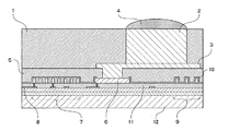
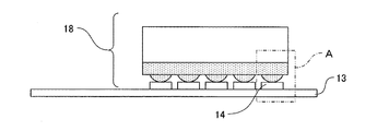
ここで、従来の半導体装置について図10、図11、図12、図13を用いて詳細に説明する。
図10は従来の半導体装置の構成を示す要部断面図とそれに対応した配線配置図、図11は従来のWLCSPの実装状態を示す図、図12は従来のWLCSPの実装状態を示す要部拡大図、図13は従来のWLCSPの実装時の半導体配線付近に印加される荷重と応力集中箇所を示す図である。
Here, a conventional semiconductor device will be described in detail with reference to FIG. 10, FIG. 11, FIG. 12, and FIG.
FIG. 10 is a cross-sectional view of a main part showing a configuration of a conventional semiconductor device and a wiring layout corresponding thereto, FIG. 11 is a diagram showing a mounting state of a conventional WLCSP, and FIG. 12 is an enlarged main part showing a mounting state of the conventional WLCSP. FIGS. 13A and 13B are diagrams showing a load and a stress concentration location applied to the vicinity of the semiconductor wiring when the conventional WLCSP is mounted.
また、図12は図11中のA部の拡大図、図13は、図12中のB部の拡大図である。
図10、図11、図12、図13において、1は封止樹脂、2はポスト、3は再配線、4は半田バンプ、5は絶縁膜、6はAl配線パッド、7はAl配線インダクター、8は第1の信号配線、9は第2の信号配線、10は表面保護膜、11は層間絶縁膜、12は半導体基板、13は実装基板、14は実装基板端子、17はクラック、18はWLCSP、19は応力集中箇所である。
12 is an enlarged view of a portion A in FIG. 11, and FIG. 13 is an enlarged view of a portion B in FIG.
10, 11, 12, and 13, 1 is a sealing resin, 2 is a post, 3 is a rewiring, 4 is a solder bump, 5 is an insulating film, 6 is an Al wiring pad, 7 is an Al wiring inductor, 8 is the first signal wiring, 9 is the second signal wiring, 10 is the surface protection film, 11 is the interlayer insulating film, 12 is the semiconductor substrate, 13 is the mounting substrate, 14 is the mounting substrate terminal, 17 is the crack, 18 is WLCSP and 19 are stress concentration points.
まず、従来の半導体装置の構成について図10を用いて説明する。図10に示すように半導体装置は、半導体基板12上に、例えば、MOS型トランジスタのような半導体素子や、PN接合にて形成されているダイオード、バイポーラ型トランジスタなどの半導体素子が形成されている。半導体基板12上を層間膜絶縁膜11で覆い半導体素子を保護している。また、半導体素子から信号を導通するための第1の信号配線8や、多層配線技術を用いて第1の信号配線8上に層間絶縁膜11にて電気的に絶縁された第2の信号配線9や、Al配線インダクター7、外部へ信号を取り出す為のAl配線パッド6が配置されている。これらのものは、表面保護膜10により、電気的、又は、外界からの雰囲気的に絶縁され保護される。
First, the structure of a conventional semiconductor device will be described with reference to FIG. As shown in FIG. 10, in the semiconductor device, for example, a semiconductor element such as a MOS transistor, a diode formed by a PN junction, or a semiconductor element such as a bipolar transistor is formed on a
次に、Al配線パッド6から実際に外部へ信号を取り出すために、再配線3を用い、半田バンプ4下まで配線が配置されている。半田バンプ4と再配線3は、実装信頼性向上の為、ポスト2を介して接続されている。ポスト2及び再配線3は外部的衝撃や雰囲気から守るため、封止樹脂1にて保護されている。また、実装基板へ接続する接点となる半田バンプ4がポスト2上に形成されている。ここで、第2の信号配線9、Al配線パッド6、Al配線インダクター7は、インダクター特性値を考慮し、約2μm程度の厚い膜厚の配線を使用する。相対的に、第2の信号配線9に対して表面保護膜10は薄く形成される。
Next, in order to actually extract a signal from the
また、第2の信号配線9は、図11におけるA部の様なWLCSP18の再外周の端子で、図12におけるB部の様なポスト2の外周部直下に配置されている。
図11において、WLCSP18は、半田バンプ4の面を下側にして実装基板13上に形成され、実装基板端子13に載置される。その後、熱処理工程(220〜260℃)を実施し、半田バンプ4が溶融し、実装基板端子14と接合される(例えば、特許文献1参照)。
Further, the second signal wiring 9 is a terminal on the outer periphery of the
In FIG. 11, the WLCSP 18 is formed on the
図13は、WLCSP18は半田バンプ4を配置しているWLCSP18の再外周部分に配置されている半田バンプ4及びポスト2下に配置された第2の信号配線9及び表面保護膜10について、熱処理工程時に発生する周辺の部材の荷重の印加状態と、応力集中箇所19の位置を示したものである。
しかしながら、従来のWLCSPにおいて、図10及び図13に示す第2の信号配線9がポスト2の外周部直下に配置された場合において、そのポスト2が、WLCSP18の出力端子が並んでいるパッケージの外周部に配置された時、WLCSP18を実装基板13に実装し、熱処理後、WLCSPの場合は、パッケージに使用するパッケージ内配線を第2の信号線9と表面保護膜10上に直接形成することを特徴とするパッケージの為、第2の信号配線9や表面保護膜10に表面保護膜10を破壊する様な大きさの応力が発生し、表面保護膜10にクラック17が発生するという問題点があった。
However, in the conventional WLCSP, when the second signal wiring 9 shown in FIGS. 10 and 13 is arranged immediately below the outer periphery of the
本発明の半導体装置は、前記従来技術の問題を解決することに指向するものであり、外形の変更や新たな工程や費用を発生させることなく、クラックの発生を抑制することを目的とする。 The semiconductor device of the present invention is directed to solving the above-described problems of the prior art, and aims to suppress the occurrence of cracks without causing a change in outer shape, new processes, and costs.
前記の目的を達成するために、本発明に係る請求項1に記載された半導体装置は、外部端子を備えるウェハレベルチップスケールパッケージ構造の半導体装置であって、基板平面と平行な平面で、隣接する前記外部端子の重心を結ぶ線上と前記半導体装置のパッケージ端との間の領域を信号配線禁止領域と想定し、前記信号配線禁止領域に配置される信号配線と、前記信号配線の周囲の同一配線層に配置されるダミー配線とを有することを特徴とする。
In order to achieve the above object, a semiconductor device according to
請求項2に記載された半導体装置は、外部端子を備えるウェハレベルチップスケールパッケージ構造の半導体装置であって、前記半導体装置のパッケージ端から基板平面と平行な平面で前記外部端子の重心に垂線を引き、前記垂線を中心に前記重心から140°の扇角を持った範囲と、前記重心を中心に前記外部端子端までの最短の長さの5分の4を半径とした円弧と前記重心を中心に前記外部端子端までの最長の長さの5分の6を半径とした円弧とで囲まれた範囲とが重なる領域を信号配線禁止領域と想定し、前記信号配線禁止領域に配置される信号配線と、前記信号配線と同一配線層の周囲に配置されるダミー配線とを有することを特徴とする。
The semiconductor device according to
請求項3に記載された半導体装置は、基板主面と平行な平面が円形形状のバンプにより形成される外部端子を備えるウェハレベルチップスケールパッケージ構造の半導体装置であって、隣接する前記外バンプの基板平面と平行な平面での中心を結ぶ線上と前記半導体装置のパッケージ端との間の領域を信号配線禁止領域と想定し、前記信号配線禁止領域に配置される信号配線と、前記信号配線の周囲の同一配線層に配置されるダミー配線とを有することを特徴とする。
The semiconductor device according to
請求項4に記載された半導体装置は、基板主面と平行な平面が円形形状のバンプにより形成される外部端子を備えるウェハレベルチップスケールパッケージ構造の半導体装置であって、前記半導体装置のパッケージ端から前記外部端子の平面円の中心に垂線を引き、前記垂線を中心に前記平面円の中心から140°の扇角を持った範囲と、前記平面円の中心を中心に前記外部端子半径の5分の4の円弧と前記平面円の中心を中心に前記外部端子半径の5分の6の円弧とで囲まれた範囲とが重なる領域を信号配線禁止領域と想定し、前記信号配線禁止領域に配置される信号配線と、前記信号配線と同一配線層の周囲に配置されるダミー配線とを有することを特徴とする。
5. The semiconductor device according to
請求項5に記載された半導体装置は、請求項3または請求項4のいずれかに記載の半導体装置において、前記バンプの下層にポストを備えることを特徴とする。
請求項6に記載された半導体装置は、請求項3または請求項4のいずれかに記載の半導体装置において、前記バンプの下層にアンダーバンプメタル膜を備えることを特徴とする。
A semiconductor device according to a fifth aspect is the semiconductor device according to the third or fourth aspect, wherein a post is provided below the bump.
A semiconductor device according to a sixth aspect is the semiconductor device according to the third or fourth aspect, wherein an under bump metal film is provided below the bump.
請求項7に記載された半導体装置は、請求項1〜請求項6のいずれかに記載の半導体装置において、前記ダミー配線が、前記信号配線と2μm以上の隙間を開け、前記信号配線の周囲を連続的に囲っている事を特徴とする。 A semiconductor device according to a seventh aspect is the semiconductor device according to any one of the first to sixth aspects, wherein the dummy wiring opens a gap of 2 μm or more from the signal wiring to surround the signal wiring. It is characterized by being surrounded continuously.
請求項8に記載された半導体装置は、請求項1〜請求項6のいずれかに記載の半導体装置において、前記ダミー配線が、前記信号配線の幅寸法以上の隙間を開け、前記信号配線に平行して1または複数本配置される事を特徴とする。
The semiconductor device according to
請求項9に記載された半導体装置は、請求項1〜請求項6のいずれかに記載の半導体装置において、前記ダミー配線が、前記信号配線と2μm以上の隙間を開け、前記信号配線に平行して1または複数本配置される事を特徴とする。 A semiconductor device according to a ninth aspect is the semiconductor device according to any one of the first to sixth aspects, wherein the dummy wiring opens a gap of 2 μm or more from the signal wiring and is parallel to the signal wiring. One or a plurality of them are arranged.
請求項10に記載された半導体装置は、外部端子を備えるウェハレベルチップスケールパッケージ構造の半導体装置であって、基板平面と平行な平面で隣接する前記外部端子の重心を結ぶ線上と前記半導体装置のパッケージ端との間の領域を信号配線禁止領域と想定し、前記信号配線禁止領域に配置される信号配線の線幅を前記信号配線の厚みの5倍以上の幅にすることを特徴とする。
The semiconductor device according to
請求項11に記載された半導体装置は、外部端子を備えるウェハレベルチップスケールパッケージ構造の半導体装置であって、前記半導体装置のパッケージ端から基板平面と平行な平面で前記外部端子の重心に垂線を引き、前記垂線を中心に前記重心から140°の扇角を持った範囲と、前記重心を中心に前記外部端子端までの最短の長さの5分の4を半径とした円弧と前記重心を中心に前記外部端子端までの最長の長さの5分の6を半径とした円弧とで囲まれた範囲とが重なる領域を信号配線禁止領域と想定し、前記信号配線禁止領域に配置される信号配線の線幅を前記信号配線の厚みの5倍以上の幅にすることを特徴とする。
The semiconductor device according to
請求項12に記載された半導体装置は、基板主面と平行な平面が円形形状のバンプにより形成される外部端子を備えるウェハレベルチップスケールパッケージ構造の半導体装置であって、隣接する前記外バンプの基板平面と平行な平面での中心を結ぶ線上と前記半導体装置のパッケージ端との間の領域を信号配線禁止領域と想定し、前記信号配線禁止領域に配置される信号配線の線幅を前記信号配線の厚みの5倍以上の幅にすることを特徴とする。
A semiconductor device according to
請求項13に記載された半導体装置は、基板主面と平行な平面が円形形状のバンプにより形成される外部端子を備えるウェハレベルチップスケールパッケージ構造の半導体装置であって、前記半導体装置のパッケージ端から前記外部端子の平面円の中心に垂線を引き、前記垂線を中心に前記平面円の中心から140°の扇角を持った範囲と、前記平面円の中心を中心に前記外部端子半径の5分の4の円弧と前記平面円の中心を中心に前記外部端子半径の5分の6の円弧とで囲まれた範囲とが重なる領域を信号配線禁止領域と想定し、前記信号配線禁止領域に配置される信号配線の線幅を前記信号配線の厚みの5倍以上の幅にすることを特徴とする。
A semiconductor device according to
請求項14に記載された半導体装置は、請求項12または請求項13のいずれかに記載の半導体装置において、前記バンプの下層にポストを備えることを特徴とする。
請求項15に記載された半導体装置は、請求項12または請求項13のいずれかに記載の半導体装置において、前記バンプの下層にアンダーバンプメタル膜を備えることを特徴とする。
A semiconductor device according to a fourteenth aspect is the semiconductor device according to the twelfth or thirteenth aspect, wherein a post is provided below the bump.
According to a fifteenth aspect of the present invention, in the semiconductor device according to the twelfth or thirteenth aspect, an under bump metal film is provided below the bump.
請求項16に記載された半導体装置は、請求項10〜請求項15のいずれかに記載の半導体装置において、前記信号配線禁止領域に配置される信号配線の線幅を10μm以上にすることを特徴とする。 A semiconductor device according to a sixteenth aspect is the semiconductor device according to any one of the tenth to fifteenth aspects, wherein a line width of the signal wiring arranged in the signal wiring prohibition region is 10 μm or more. And
請求項17に記載された半導体装置は、請求項1〜請求項16のいずれかに記載の半導体装置において、前記複数の配線は、Alを含んだ材料であり、厚さは1.5μm以上であることを特徴とする。
The semiconductor device according to
以上により、外形の変更や新たな工程や費用を発生させることなく、クラックの発生を抑制することができる。 As described above, it is possible to suppress the occurrence of cracks without generating a change in the outer shape, a new process, or a cost.
本発明によれば、ウェハレベルCSPパッケージにおいて、パッケージ外周部分に配置される外部出力端子近傍の配線禁止領域に配置される信号配線に対して、その周囲にダミー配線を配置、あるいは信号配線自体の幅を大きくすることにより、信号配線に発生する応力を分散することができるため、容易に、表面保護膜のクラックの発生を抑制することができる。 According to the present invention, in the wafer level CSP package, dummy wiring is arranged around the signal wiring arranged in the wiring prohibition area near the external output terminal arranged in the outer periphery of the package, or the signal wiring itself is arranged. By increasing the width, it is possible to disperse the stress generated in the signal wiring, so that the occurrence of cracks in the surface protective film can be easily suppressed.
以下、図面を参照して本発明における実施の形態を詳細に説明する。
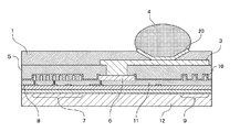
図1は本発明の半導体装置の構成を示す要部断面図である。また、図2は半導体装置の構成を示す要部断面図とそれに対応した配線配置平面図である。図3は本発明の半導体装置における信号配線配置禁止領域をWLCSP内で説明する図、図4は本発明の半導体装置における信号配線配置禁止領域におけるWLCSPの端面の近さを説明する図、図5は本発明の半導体装置における信号配線配置禁止領域を説明する図である。図6は第一の実施の形態における信号配線配置禁止領域の信号配線の構成を示す図である。図7は第二の実施の形態における信号配線配置禁止領域の信号配線の構成を示す図である。図8は第三の実施の形態における信号配線配置禁止領域の信号配線の構成を示す図である。図9は第四の実施の形態における半導体装置の構成を示す要部断面図である。
Hereinafter, embodiments of the present invention will be described in detail with reference to the drawings.
FIG. 1 is a cross-sectional view of the main part showing the configuration of the semiconductor device of the present invention. FIG. 2 is a cross-sectional view of a main part showing the configuration of the semiconductor device and a wiring layout plan view corresponding to the cross-sectional view. 3 is a diagram for explaining the signal wiring arrangement prohibited region in the WLCSP in the semiconductor device of the present invention, FIG. 4 is a diagram for explaining the proximity of the end face of the WLCSP in the signal wiring arrangement prohibited region in the semiconductor device of the present invention, FIG. These are diagrams for explaining a signal wiring arrangement prohibition region in the semiconductor device of the present invention. FIG. 6 is a diagram showing a configuration of signal wirings in the signal wiring arrangement prohibition region in the first embodiment. FIG. 7 is a diagram showing a configuration of signal wirings in the signal wiring arrangement prohibition region in the second embodiment. FIG. 8 is a diagram showing a configuration of signal wirings in the signal wiring arrangement prohibition region in the third embodiment. FIG. 9 is a fragmentary cross-sectional view showing the configuration of the semiconductor device according to the fourth embodiment.
ここで、前記背景技術を示す図10において説明した構成部材に対応し、同等の機能を有するものには同一の符号を付して示す。
図1、図2、図3、図4、図5、図6、図7、図8、図9において、1は封止樹脂、2はポスト、3は再配線、4は平面形状が円形の半田バンプ、5は絶縁膜、6はAl配線パッド、7はAl配線インダクター、8は第1の信号配線、9は第2の信号配線、10は表面保護膜、11は層間絶縁膜、12は半導体基板、15は表面に半田バンプ4が形成されたWLCSPの半田バンプ4形成領域近傍のWLCSP側面、16は信号配線配置禁止領域、20はUBM(アンダーバンプメタル膜)である。なお、第2の信号配線9のなかで、電気信号を流す実配線を配線9b、電気信号を流さないダミー配線を配線9a、配線9cとする。
Here, components corresponding to the constituent members described in FIG. 10 showing the background art and having equivalent functions are denoted by the same reference numerals.
1, 2, 3, 4, 5, 6, 7, 8, and 9, 1 is a sealing resin, 2 is a post, 3 is a rewiring, and 4 is a circular planar shape. Solder bumps, 5 an insulating film, 6 an Al wiring pad, 7 an Al wiring inductor, 8 a first signal wiring, 9 a second signal wiring, 10 a surface protective film, 11 an interlayer insulating film, and 12 a A semiconductor substrate, 15 is a WLCSP side surface in the vicinity of a
図1及び図2に示すように、本発明における半導体装置は、半導体基板12上に、例えば、MOS型トランジスタのような半導体素子や、PN接合にて形成されているダイオード、バイポーラ型トランジスタなどの半導体素子が形成されている。半導体基板12上を層間膜絶縁膜11で覆い半導体素子を保護している。また、半導体素子から信号を導通するための第1の信号配線8や、多層配線技術を用いて、第1の信号配線8上に、層間絶縁膜11にて電気的に絶縁された、第2の信号配線9や、Al配線インダクター7、外部へ信号を取り出す為のAl配線パッド6が配置されている。これらのものは、表面保護膜10により、電気的、又は、外界からの雰囲気的に絶縁され保護される。ここで、第2の信号配線9の配線材料はAlを含んだ材料であることが望ましく、第2の信号配線9、Al配線パッド6、Al配線インダクター7は、インダクター特性値を考慮し、約1.5μm以上の厚い膜厚の配線を使用する。そして、第2の信号配線9に対して、相対的に、表面保護膜10は薄く形成される。
As shown in FIGS. 1 and 2, the semiconductor device according to the present invention includes, for example, a semiconductor element such as a MOS transistor, a diode formed by a PN junction, a bipolar transistor, and the like on a
また、Al配線パッド6から、実際に外部へ信号を取り出すために、再配線3を用い配線を半田バンプ4下まで配置している。半田バンプ4と再配線3は、実装信頼性向上の為、ポスト2を介して接続されている。ポスト2及び再配線3は外部的衝撃や雰囲気から守るため、封止樹脂1にて保護されている。実装基板へ接続する接点となる半田バンプ4がポスト2上に形成されている。
Further, in order to actually extract a signal from the
ここで、第2の信号配線9は、ポスト2の外周部直下に配置されており、信号配線9bは実際に信号を伝える為の配線である。また、信号配線9a、9cはダミー配線であり、信号の伝達には用いない配線である。
Here, the second signal wiring 9 is disposed immediately below the outer peripheral portion of the
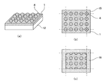
図3は信号配線領域16をWLCSPのどの部分に当たるかを説明する為の図である。
図3(a)はWLCSP全体を半田バンプ形成面から見た斜視図、図3(b)はWLCSP側面部15と周辺の端子の中心を表す図面、図3(c)はWLCSP側面部15と周辺の端子の中心からなる信号配線配置禁止領域16を表す図面、図4は信号配線配置禁止領域16について、図3の拡大として、WLCSPの端に近い側のポスト2の半分側を説明する図である。
FIG. 3 is a diagram for explaining to which part of the WLCSP the
3A is a perspective view of the entire WLCSP as viewed from the solder bump forming surface, FIG. 3B is a drawing showing the center of the WLCSP
図3に示すように、WLCSPにおける最外周の端子の中心を結ぶ線とWLCSP側面15の間をWLCSP内での信号配線配置禁止領域16と設定する。
言い換えると、図4に示すように、信号配線配置禁止領域16は、WLCSP側面15からポスト2の中心までに位置される事を示す。
As shown in FIG. 3, a signal wiring
In other words, as shown in FIG. 4, the signal wiring
図5は、信号配線配置禁止領域16について、さらに範囲を限定する場合を説明するものであり、その為、ポスト2を抜き出したものである。WLCSP側面15、つまり、パッケージの側面に近い半田バンプ4(図1参照)及びポスト2から形成されるWLCSPの外部端子において、WLCSP側面15から、半田バンプ4つまりポスト2の半導体基板と平行な平面における平面円形の中心点(以下平面円の中心と称す)に垂線を引きだす。半田バンプ4の平面円の中心を中心点として垂線から左右70°開いた扇形状領域と、平面中心からの半径が半田パンプ4の半径の5分の4〜5分の6の領域との重なった部分を信号配線配置禁止領域16とする。
FIG. 5 illustrates a case where the range of the signal wiring
このように図3〜図5に示す信号配線禁止領域16に、配線9bを単独で配置した場合が従来の半導体装置であるが、配線9bを単独とせず、配線9a、9cを同時に配置する事により、配線9bに直接応力が発生することなく、配線9a、配線9cに応力が分散するため、配線9b周りの保護膜10の破壊を防ぐ事が可能となる。
As described above, when the
本発明は、熱処理により応力が集中して発生する信号配線配置禁止領域16に第2の信号配線9を配置する際に、実動作に用いられる配線9bとその周囲にダミー配線9a等を設けることにより、熱処理時の応力を分散することができるため、外形の変更や新たな工程や費用を発生させることなく、実動作に用いられる表面保護膜にクラックが発生することを抑制することができる。
In the present invention, when the second signal wiring 9 is arranged in the signal wiring
ここで、実配線とダミー配線との間隔を配線幅以上、例えば配線幅が2.0μmの場合には2.0μm以上とすることが望ましい。配線幅以上間隔を開けることにより、配線9bに直接応力が発生することなく、配線9a、配線9cに応力が分散されるため、配線9b周りの保護膜10の破壊を防ぐ事が可能となる。
Here, the interval between the actual wiring and the dummy wiring is preferably equal to or larger than the wiring width, for example, 2.0 μm or more when the wiring width is 2.0 μm. Since the stress is distributed to the
以下、信号配線配置禁止領域16における第2の信号配線9の構成についての具体的な実施の形態について詳細に説明する。
(第一の実施の形態)
図6は、第一の実施の形態を示すものである。第2の信号配線9がポスト2のWLCSP側面15付近の信号配線配置禁止領域16に配置されている。第2の信号配線9のなかで、電気信号を流す実配線を配線9b、電気信号を流さないダミー配線を配線9a、9cとする。電気信号を流す第2の信号配線9bの両側に、電気信号を流さない配線9a及び9cが配置される事によって、WLCSP実装時の熱処理工程により発生する応力が、第2の信号配線9bのみならず第2の信号配線9a、第2の信号配線9cに分散されて第2の信号配線9b単体に発生する応力が減少する。このことより、第2の信号配線9全体に均一に応力が発生し、表面保護膜10にクラックが発生することを抑制し、信頼性に優れた半導体装置を提供する事が可能となる。
Hereinafter, a specific embodiment of the configuration of the second signal wiring 9 in the signal wiring
(First embodiment)
FIG. 6 shows the first embodiment. The second signal wiring 9 is arranged in the signal wiring
ここでは、実配線をはさんで平行にダミー配線を2本配置する例を説明したが、実配線に平行に配置されるダミー配線は1本でも良く、2本以上配置しても良い。
(第二の実施の形態)
図7は、第二の実施の形態を示すものである。第2の信号配線9がポスト2のWLCSP側面15付近の信号配線配置禁止領域16に配置されている。第2の信号配線9のなかで、電気信号を流す実配線を配線9b、電気信号を流さないダミー配線を配線9aとする。電気信号を流す第2の信号配線9bの周囲を連続的に囲むように、電気信号を流さない配線9aが配置される事によって、WLCSP実装時の熱処理工程により発生する応力が第2の信号配線9b単体のみならず第2の信号配線9aに分散されて第2の信号配線9b単体に発生する応力が減少する。このことより、第2の信号配線9全体に均一に応力が発生し、表面保護膜10にクラックが発生することを抑制し、信頼性に優れた半導体装置を提供する事が可能となる。
Here, an example has been described in which two dummy wirings are arranged in parallel across the actual wiring. However, one dummy wiring may be arranged in parallel to the actual wiring, or two or more dummy wirings may be arranged.
(Second embodiment)
FIG. 7 shows a second embodiment. The second signal wiring 9 is arranged in the signal wiring
(第三の実施の形態)
図8は、第三の実施の形態を示すものである。第2の信号配線9がポスト2のWLCSP側面15付近の信号配線配置禁止領域16に配置されている。電気信号を流して実動作に用いる第2の信号配線9は、配線幅を10μm以上確保する。配線幅が10μm以上あることにより、WLCSP実装時の熱処理工程により発生する応力が、第2の信号配線9が一般的な2μm幅の場合より、第2の信号配線9の幅が10μm分に分散される。このことより、第2の信号配線9全体に均一に応力が発生し、表面保護膜10にクラックが発生することを抑制し、信頼性に優れた半導体装置を提供する事が可能となる。
(Third embodiment)
FIG. 8 shows a third embodiment. The second signal wiring 9 is arranged in the signal wiring
また、配線幅として、信号配線の厚みの5倍にすることにより、信号配線の横方向に発生する応力が小さくなるため、同様の効果を得ることができる。
(第四の実施の形態)
図9は、第四の実施の形態を示すものである。なお、図1と同じ構成部材については同じ符号を付し、説明を省略する。
Further, by setting the wiring width to 5 times the thickness of the signal wiring, the stress generated in the lateral direction of the signal wiring is reduced, so that the same effect can be obtained.
(Fourth embodiment)
FIG. 9 shows a fourth embodiment. In addition, the same code | symbol is attached | subjected about the same component as FIG. 1, and description is abbreviate | omitted.
第四の実施の形態におけるWLCSPは、ポスト2を有しない形態であり、上述のWLCSPに対して、再配線3の上に、直接半田バンプ4をポスト2の代わりにUBM20上に形成されている。
The WLCSP in the fourth embodiment is a form not having the
このような形態のWLCSPにおいても、信号配線配置禁止領域16に、第一の実施の形態〜第三の実施の形態におけるような、ダミー配線9aあるいはダミー配線9bを設けたり、電気信号を流して実動作に用いる第2の信号配線9の配線幅を10μm以上確保したりすることにより、WLCSP実装時の熱処理工程により発生する応力が分散される。このことより、第一の実施の形態〜第三の実施の形態と同様に表面保護膜10にクラックが発生することを抑制し、信頼性に優れた半導体装置を提供する事が可能となる。
Even in such a form of WLCSP, the
同様に、平面中心からの半径が半田パンプの半径の5分の4〜5分の6の領域との重なった部分を、重心を中心に外部端子端までの最短の長さの5分の4を半径とした円弧と重心を中心に外部端子端までの最長の長さの5分の6を半径とした円弧とで囲まれた範囲とすることができる。 Similarly, a portion where the radius from the center of the plane overlaps the region of 4/5 to 6/5 of the radius of the solder bump is 4/5 of the shortest length from the center of gravity to the end of the external terminal. And a circle surrounded by an arc having a radius of 6/5 of the longest length from the center of gravity to the external terminal end.
本発明は、クラックの発生を抑制することができ、半導体チップ状態で樹脂封止された、ウェハレベルチップスケールパッケージ構造の半導体装置等に有用である。 INDUSTRIAL APPLICABILITY The present invention can suppress the occurrence of cracks and is useful for a semiconductor device having a wafer level chip scale package structure that is resin-sealed in a semiconductor chip state.
1 封止樹脂
2 ポスト
3 再配線
4 半田バンプ
5 絶縁膜
6 Al配線パッド
7 Al配線インダクター
8 第1の信号配線
9 第2の信号配線
9a 配線
9b 配線
9c 配線
10 表面保護膜
11 層間絶縁膜
12 半導体基板
13 実装基板
14 実装基板端子
15 WLCSP側面
16 信号配線配置禁止領域
17 クラック
18 WLCSP
19 応力集中箇所
20 UBM
DESCRIPTION OF
19
Claims (17)
基板平面と平行な平面で、隣接する前記外部端子の重心を結ぶ線上と前記半導体装置のパッケージ端との間の領域を信号配線禁止領域と想定し、
前記信号配線禁止領域に配置される信号配線と、
前記信号配線の周囲の同一配線層に配置されるダミー配線とを有することを特徴とする半導体装置。 A semiconductor device having a wafer level chip scale package structure including an external terminal,
Assuming that the area between the line connecting the centroids of the adjacent external terminals and the package end of the semiconductor device is a signal wiring prohibited area in a plane parallel to the substrate plane,
A signal wiring disposed in the signal wiring prohibited area;
And a dummy wiring arranged in the same wiring layer around the signal wiring.
前記半導体装置のパッケージ端から基板平面と平行な平面で前記外部端子の重心に垂線を引き、前記垂線を中心に前記重心から140°の扇角を持った範囲と、前記重心を中心に前記外部端子端までの最短の長さの5分の4を半径とした円弧と前記重心を中心に前記外部端子端までの最長の長さの5分の6を半径とした円弧とで囲まれた範囲とが重なる領域を信号配線禁止領域と想定し、
前記信号配線禁止領域に配置される信号配線と、
前記信号配線と同一配線層の周囲に配置されるダミー配線とを有することを特徴とする半導体装置。 A semiconductor device having a wafer level chip scale package structure including an external terminal,
A perpendicular line is drawn from the package end of the semiconductor device to the center of gravity of the external terminal in a plane parallel to the substrate plane, the range having a fan angle of 140 ° from the center of gravity about the perpendicular, and the external center around the center of gravity. A range surrounded by an arc whose radius is 4/5 of the shortest length to the terminal end and an arc whose radius is 6/5 of the longest length to the external terminal end centered on the center of gravity. Assuming that the area where the
A signal wiring disposed in the signal wiring prohibited area;
A semiconductor device comprising the signal wiring and a dummy wiring arranged around the same wiring layer.
隣接する前記外バンプの基板平面と平行な平面での中心を結ぶ線上と前記半導体装置のパッケージ端との間の領域を信号配線禁止領域と想定し、
前記信号配線禁止領域に配置される信号配線と、
前記信号配線の周囲の同一配線層に配置されるダミー配線とを有することを特徴とする半導体装置。 A semiconductor device having a wafer level chip scale package structure including an external terminal having a plane parallel to the substrate main surface formed by circular bumps,
Assuming a region between a line connecting the centers of adjacent outer bumps in a plane parallel to the substrate plane and a package end of the semiconductor device as a signal wiring prohibited region,
A signal wiring disposed in the signal wiring prohibited area;
And a dummy wiring arranged in the same wiring layer around the signal wiring.
前記半導体装置のパッケージ端から前記外部端子の平面円の中心に垂線を引き、前記垂線を中心に前記平面円の中心から140°の扇角を持った範囲と、前記平面円の中心を中心に前記外部端子半径の5分の4の円弧と前記平面円の中心を中心に前記外部端子半径の5分の6の円弧とで囲まれた範囲とが重なる領域を信号配線禁止領域と想定し、
前記信号配線禁止領域に配置される信号配線と、
前記信号配線と同一配線層の周囲に配置されるダミー配線とを有することを特徴とする半導体装置。 A semiconductor device having a wafer level chip scale package structure including an external terminal having a plane parallel to the substrate main surface formed by circular bumps,
A perpendicular line is drawn from the package end of the semiconductor device to the center of the planar circle of the external terminal, a range having a fan angle of 140 ° from the center of the planar circle around the perpendicular, and the center of the planar circle Assuming a region where the arc surrounded by the arc of 4/5 of the external terminal radius and the arc of 6/5 of the external terminal radius centered on the center of the plane circle is a signal wiring prohibited region,
A signal wiring disposed in the signal wiring prohibited area;
A semiconductor device comprising the signal wiring and a dummy wiring arranged around the same wiring layer.
基板平面と平行な平面で隣接する前記外部端子の重心を結ぶ線上と前記半導体装置のパッケージ端との間の領域を信号配線禁止領域と想定し、
前記信号配線禁止領域に配置される信号配線の線幅を前記信号配線の厚みの5倍以上の幅にすることを特徴とする半導体装置。 A semiconductor device having a wafer level chip scale package structure including an external terminal,
Assuming a region between the line connecting the centroids of the external terminals adjacent in a plane parallel to the substrate plane and the package end of the semiconductor device as a signal wiring prohibited region,
A semiconductor device characterized in that a line width of a signal wiring arranged in the signal wiring prohibition region is set to a width of 5 times or more a thickness of the signal wiring.
前記半導体装置のパッケージ端から基板平面と平行な平面で前記外部端子の重心に垂線を引き、前記垂線を中心に前記重心から140°の扇角を持った範囲と、前記重心を中心に前記外部端子端までの最短の長さの5分の4を半径とした円弧と前記重心を中心に前記外部端子端までの最長の長さの5分の6を半径とした円弧とで囲まれた範囲とが重なる領域を信号配線禁止領域と想定し、
前記信号配線禁止領域に配置される信号配線の線幅を前記信号配線の厚みの5倍以上の幅にすることを特徴とする半導体装置。 A semiconductor device having a wafer level chip scale package structure including an external terminal,
A perpendicular line is drawn from the package end of the semiconductor device to the center of gravity of the external terminal in a plane parallel to the substrate plane, the range having a fan angle of 140 ° from the center of gravity about the perpendicular, and the external center around the center of gravity. A range surrounded by an arc having a radius of 4/5 of the shortest length to the terminal end and an arc having a radius of 6/5 of the longest length to the external terminal center around the center of gravity. Assuming that the area where the
A semiconductor device characterized in that a line width of a signal wiring arranged in the signal wiring prohibition region is set to a width of 5 times or more a thickness of the signal wiring.
隣接する前記外バンプの基板平面と平行な平面での中心を結ぶ線上と前記半導体装置のパッケージ端との間の領域を信号配線禁止領域と想定し、
前記信号配線禁止領域に配置される信号配線の線幅を前記信号配線の厚みの5倍以上の幅にすることを特徴とする半導体装置。 A semiconductor device having a wafer level chip scale package structure including an external terminal having a plane parallel to the substrate main surface formed by circular bumps,
Assuming a region between a line connecting the centers of adjacent outer bumps in a plane parallel to the substrate plane and a package end of the semiconductor device as a signal wiring prohibited region,
A semiconductor device characterized in that a line width of a signal wiring arranged in the signal wiring prohibition region is set to a width of 5 times or more a thickness of the signal wiring.
前記半導体装置のパッケージ端から前記外部端子の平面円の中心に垂線を引き、前記垂線を中心に前記平面円の中心から140°の扇角を持った範囲と、前記平面円の中心を中心に前記外部端子半径の5分の4の円弧と前記平面円の中心を中心に前記外部端子半径の5分の6の円弧とで囲まれた範囲とが重なる領域を信号配線禁止領域と想定し、
前記信号配線禁止領域に配置される信号配線の線幅を前記信号配線の厚みの5倍以上の幅にすることを特徴とする半導体装置。 A semiconductor device having a wafer level chip scale package structure including an external terminal having a plane parallel to the substrate main surface formed by circular bumps,
A perpendicular line is drawn from the package end of the semiconductor device to the center of the planar circle of the external terminal, a range having a fan angle of 140 ° from the center of the planar circle around the perpendicular, and the center of the planar circle Assuming a region where the arc surrounded by the arc of 4/5 of the external terminal radius and the arc of 6/5 of the external terminal radius centered on the center of the plane circle is a signal wiring prohibited region,
A semiconductor device characterized in that a line width of a signal wiring arranged in the signal wiring prohibition region is set to a width of 5 times or more a thickness of the signal wiring.
Priority Applications (2)
| Application Number | Priority Date | Filing Date | Title |
|---|---|---|---|
| JP2008133712A JP2009111333A (en) | 2007-10-12 | 2008-05-22 | Semiconductor device |
| US12/207,790 US8084859B2 (en) | 2007-10-12 | 2008-09-10 | Semiconductor device |
Applications Claiming Priority (2)
| Application Number | Priority Date | Filing Date | Title |
|---|---|---|---|
| JP2007265973 | 2007-10-12 | ||
| JP2008133712A JP2009111333A (en) | 2007-10-12 | 2008-05-22 | Semiconductor device |
Publications (2)
| Publication Number | Publication Date |
|---|---|
| JP2009111333A true JP2009111333A (en) | 2009-05-21 |
| JP2009111333A5 JP2009111333A5 (en) | 2011-06-23 |
Family
ID=40779469
Family Applications (1)
| Application Number | Title | Priority Date | Filing Date |
|---|---|---|---|
| JP2008133712A Pending JP2009111333A (en) | 2007-10-12 | 2008-05-22 | Semiconductor device |
Country Status (1)
| Country | Link |
|---|---|
| JP (1) | JP2009111333A (en) |
Cited By (3)
| Publication number | Priority date | Publication date | Assignee | Title |
|---|---|---|---|---|
| JP2013508954A (en) * | 2009-10-23 | 2013-03-07 | エーティーアイ・テクノロジーズ・ユーエルシー | Routing layer to reduce stress in semiconductor dies |
| US9035471B2 (en) | 2009-10-23 | 2015-05-19 | Ati Technologies Ulc | Routing layer for mitigating stress in a semiconductor die |
| JP2016518730A (en) * | 2013-05-20 | 2016-06-23 | クアルコム,インコーポレイテッド | Semiconductor device with mold for top and side wall protection |
Citations (10)
| Publication number | Priority date | Publication date | Assignee | Title |
|---|---|---|---|---|
| JPS6314452A (en) * | 1986-07-04 | 1988-01-21 | Hitachi Chem Co Ltd | Semiconductor device |
| JPH0338043A (en) * | 1989-07-05 | 1991-02-19 | Hitachi Ltd | Semiconductor integrated circuit device |
| JPH0574770A (en) * | 1991-07-09 | 1993-03-26 | Yamaha Corp | Semiconductor device |
| JPH05109813A (en) * | 1991-10-19 | 1993-04-30 | Nec Corp | Semiconductor device |
| JP2003068734A (en) * | 2001-08-23 | 2003-03-07 | Seiko Epson Corp | Semiconductor device and method of manufacturing the same |
| JP2003318177A (en) * | 2002-04-19 | 2003-11-07 | Sharp Corp | Semiconductor integrated circuit device |
| JP2004273591A (en) * | 2003-03-06 | 2004-09-30 | Seiko Epson Corp | Semiconductor device and its fabricating process |
| JP2005050963A (en) * | 2003-07-31 | 2005-02-24 | Seiko Epson Corp | Semiconductor device, electronic device, electronic apparatus and manufacturing method of semiconductor device |
| JP2006032600A (en) * | 2004-07-15 | 2006-02-02 | Nec Corp | Semiconductor device |
| JP2006066505A (en) * | 2004-08-25 | 2006-03-09 | Fujikura Ltd | Semiconductor device and electronic device equipped with it |
-
2008
- 2008-05-22 JP JP2008133712A patent/JP2009111333A/en active Pending
Patent Citations (10)
| Publication number | Priority date | Publication date | Assignee | Title |
|---|---|---|---|---|
| JPS6314452A (en) * | 1986-07-04 | 1988-01-21 | Hitachi Chem Co Ltd | Semiconductor device |
| JPH0338043A (en) * | 1989-07-05 | 1991-02-19 | Hitachi Ltd | Semiconductor integrated circuit device |
| JPH0574770A (en) * | 1991-07-09 | 1993-03-26 | Yamaha Corp | Semiconductor device |
| JPH05109813A (en) * | 1991-10-19 | 1993-04-30 | Nec Corp | Semiconductor device |
| JP2003068734A (en) * | 2001-08-23 | 2003-03-07 | Seiko Epson Corp | Semiconductor device and method of manufacturing the same |
| JP2003318177A (en) * | 2002-04-19 | 2003-11-07 | Sharp Corp | Semiconductor integrated circuit device |
| JP2004273591A (en) * | 2003-03-06 | 2004-09-30 | Seiko Epson Corp | Semiconductor device and its fabricating process |
| JP2005050963A (en) * | 2003-07-31 | 2005-02-24 | Seiko Epson Corp | Semiconductor device, electronic device, electronic apparatus and manufacturing method of semiconductor device |
| JP2006032600A (en) * | 2004-07-15 | 2006-02-02 | Nec Corp | Semiconductor device |
| JP2006066505A (en) * | 2004-08-25 | 2006-03-09 | Fujikura Ltd | Semiconductor device and electronic device equipped with it |
Cited By (5)
| Publication number | Priority date | Publication date | Assignee | Title |
|---|---|---|---|---|
| JP2013508954A (en) * | 2009-10-23 | 2013-03-07 | エーティーアイ・テクノロジーズ・ユーエルシー | Routing layer to reduce stress in semiconductor dies |
| US9035471B2 (en) | 2009-10-23 | 2015-05-19 | Ati Technologies Ulc | Routing layer for mitigating stress in a semiconductor die |
| US9059159B2 (en) | 2009-10-23 | 2015-06-16 | Ati Technologies Ulc | Routing layer for mitigating stress in a semiconductor die |
| JP2016518730A (en) * | 2013-05-20 | 2016-06-23 | クアルコム,インコーポレイテッド | Semiconductor device with mold for top and side wall protection |
| US10141202B2 (en) | 2013-05-20 | 2018-11-27 | Qualcomm Incorporated | Semiconductor device comprising mold for top side and sidewall protection |
Similar Documents
| Publication | Publication Date | Title |
|---|---|---|
| US9831282B2 (en) | Electronic device package and fabricating method thereof | |
| US8084859B2 (en) | Semiconductor device | |
| US20060273463A1 (en) | Semiconductor device and mounting structure thereof | |
| US10020298B2 (en) | ESD protection device | |
| JP2009200394A (en) | Method of manufacturing semiconductor device, and semiconductor device | |
| US20170271286A1 (en) | Semiconductor device capable of dispersing stresses | |
| JP2006032453A (en) | Semiconductor device and manufacturing method thereof | |
| JP2006294704A (en) | Semiconductor device | |
| US7791187B2 (en) | Semiconductor device | |
| JP2009111333A (en) | Semiconductor device | |
| JP2005026679A (en) | Semiconductor device | |
| JP4890827B2 (en) | Semiconductor device | |
| JP2021125526A (en) | Semiconductor device and method for manufacturing semiconductor device | |
| JP2007134552A (en) | Semiconductor device | |
| CN107403764B (en) | Electronic package | |
| JP2010050136A (en) | Semiconductor device | |
| JP2007184654A (en) | Semiconductor device | |
| JP2007165800A (en) | Semiconductor chip | |
| JP2005142281A (en) | Semiconductor integrated circuit chip and semiconductor integrated circuit | |
| JP2005079431A (en) | Semiconductor device | |
| CN117096124A (en) | Electronic package and electronic structure thereof | |
| JP4240226B2 (en) | Semiconductor device and manufacturing method thereof, circuit board, and electronic apparatus | |
| JP4038691B2 (en) | Semiconductor device and manufacturing method thereof, circuit board, and electronic apparatus | |
| JP4038692B2 (en) | Semiconductor device and manufacturing method thereof, circuit board, and electronic apparatus | |
| JP2007081431A (en) | Semiconductor device, method for manufacturing it, and wire bonding chip size package equipped with it |
Legal Events
| Date | Code | Title | Description |
|---|---|---|---|
| A521 | Written amendment |
Free format text: JAPANESE INTERMEDIATE CODE: A523 Effective date: 20110511 |
|
| A621 | Written request for application examination |
Free format text: JAPANESE INTERMEDIATE CODE: A621 Effective date: 20110511 |
|
| RD03 | Notification of appointment of power of attorney |
Free format text: JAPANESE INTERMEDIATE CODE: A7423 Effective date: 20111209 |
|
| RD04 | Notification of resignation of power of attorney |
Free format text: JAPANESE INTERMEDIATE CODE: A7424 Effective date: 20111221 |
|
| RD04 | Notification of resignation of power of attorney |
Free format text: JAPANESE INTERMEDIATE CODE: A7424 Effective date: 20111222 |
|
| RD01 | Notification of change of attorney |
Free format text: JAPANESE INTERMEDIATE CODE: A7421 Effective date: 20121213 |
|
| A977 | Report on retrieval |
Free format text: JAPANESE INTERMEDIATE CODE: A971007 Effective date: 20130507 |
|
| A131 | Notification of reasons for refusal |
Free format text: JAPANESE INTERMEDIATE CODE: A131 Effective date: 20130514 |
|
| A02 | Decision of refusal |
Free format text: JAPANESE INTERMEDIATE CODE: A02 Effective date: 20131008 |