JP2008528308A - 電気処理プロファイル制御 - Google Patents
電気処理プロファイル制御 Download PDFInfo
- Publication number
- JP2008528308A JP2008528308A JP2007553195A JP2007553195A JP2008528308A JP 2008528308 A JP2008528308 A JP 2008528308A JP 2007553195 A JP2007553195 A JP 2007553195A JP 2007553195 A JP2007553195 A JP 2007553195A JP 2008528308 A JP2008528308 A JP 2008528308A
- Authority
- JP
- Japan
- Prior art keywords
- electrode
- substrate
- polishing
- biasing
- disposed
- Prior art date
- Legal status (The legal status is an assumption and is not a legal conclusion. Google has not performed a legal analysis and makes no representation as to the accuracy of the status listed.)
- Pending
Links
Images


Classifications
-
- B—PERFORMING OPERATIONS; TRANSPORTING
- B23—MACHINE TOOLS; METAL-WORKING NOT OTHERWISE PROVIDED FOR
- B23H—WORKING OF METAL BY THE ACTION OF A HIGH CONCENTRATION OF ELECTRIC CURRENT ON A WORKPIECE USING AN ELECTRODE WHICH TAKES THE PLACE OF A TOOL; SUCH WORKING COMBINED WITH OTHER FORMS OF WORKING OF METAL
- B23H5/00—Combined machining
- B23H5/06—Electrochemical machining combined with mechanical working, e.g. grinding or honing
- B23H5/08—Electrolytic grinding
-
- B—PERFORMING OPERATIONS; TRANSPORTING
- B24—GRINDING; POLISHING
- B24B—MACHINES, DEVICES, OR PROCESSES FOR GRINDING OR POLISHING; DRESSING OR CONDITIONING OF ABRADING SURFACES; FEEDING OF GRINDING, POLISHING, OR LAPPING AGENTS
- B24B37/00—Lapping machines or devices; Accessories
- B24B37/04—Lapping machines or devices; Accessories designed for working plane surfaces
- B24B37/042—Lapping machines or devices; Accessories designed for working plane surfaces operating processes therefor
-
- C—CHEMISTRY; METALLURGY
- C25—ELECTROLYTIC OR ELECTROPHORETIC PROCESSES; APPARATUS THEREFOR
- C25F—PROCESSES FOR THE ELECTROLYTIC REMOVAL OF MATERIALS FROM OBJECTS; APPARATUS THEREFOR
- C25F7/00—Constructional parts, or assemblies thereof, of cells for electrolytic removal of material from objects; Servicing or operating
-
- H—ELECTRICITY
- H01—ELECTRIC ELEMENTS
- H01L—SEMICONDUCTOR DEVICES NOT COVERED BY CLASS H10
- H01L21/00—Processes or apparatus adapted for the manufacture or treatment of semiconductor or solid state devices or of parts thereof
- H01L21/02—Manufacture or treatment of semiconductor devices or of parts thereof
- H01L21/04—Manufacture or treatment of semiconductor devices or of parts thereof the devices having at least one potential-jump barrier or surface barrier, e.g. PN junction, depletion layer or carrier concentration layer
- H01L21/18—Manufacture or treatment of semiconductor devices or of parts thereof the devices having at least one potential-jump barrier or surface barrier, e.g. PN junction, depletion layer or carrier concentration layer the devices having semiconductor bodies comprising elements of Group IV of the Periodic System or AIIIBV compounds with or without impurities, e.g. doping materials
- H01L21/30—Treatment of semiconductor bodies using processes or apparatus not provided for in groups H01L21/20 - H01L21/26
- H01L21/302—Treatment of semiconductor bodies using processes or apparatus not provided for in groups H01L21/20 - H01L21/26 to change their surface-physical characteristics or shape, e.g. etching, polishing, cutting
- H01L21/304—Mechanical treatment, e.g. grinding, polishing, cutting
-
- H—ELECTRICITY
- H01—ELECTRIC ELEMENTS
- H01L—SEMICONDUCTOR DEVICES NOT COVERED BY CLASS H10
- H01L21/00—Processes or apparatus adapted for the manufacture or treatment of semiconductor or solid state devices or of parts thereof
- H01L21/02—Manufacture or treatment of semiconductor devices or of parts thereof
- H01L21/04—Manufacture or treatment of semiconductor devices or of parts thereof the devices having at least one potential-jump barrier or surface barrier, e.g. PN junction, depletion layer or carrier concentration layer
- H01L21/18—Manufacture or treatment of semiconductor devices or of parts thereof the devices having at least one potential-jump barrier or surface barrier, e.g. PN junction, depletion layer or carrier concentration layer the devices having semiconductor bodies comprising elements of Group IV of the Periodic System or AIIIBV compounds with or without impurities, e.g. doping materials
- H01L21/30—Treatment of semiconductor bodies using processes or apparatus not provided for in groups H01L21/20 - H01L21/26
- H01L21/31—Treatment of semiconductor bodies using processes or apparatus not provided for in groups H01L21/20 - H01L21/26 to form insulating layers thereon, e.g. for masking or by using photolithographic techniques; After treatment of these layers; Selection of materials for these layers
- H01L21/3205—Deposition of non-insulating-, e.g. conductive- or resistive-, layers on insulating layers; After-treatment of these layers
- H01L21/321—After treatment
-
- C—CHEMISTRY; METALLURGY
- C25—ELECTROLYTIC OR ELECTROPHORETIC PROCESSES; APPARATUS THEREFOR
- C25D—PROCESSES FOR THE ELECTROLYTIC OR ELECTROPHORETIC PRODUCTION OF COATINGS; ELECTROFORMING; APPARATUS THEREFOR
- C25D17/00—Constructional parts, or assemblies thereof, of cells for electrolytic coating
- C25D17/10—Electrodes, e.g. composition, counter electrode
Abstract
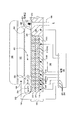
【選択図】 図6
Description
[0001]本発明の実施形態は、一般的に、基板を電気処理するためのプロファイル制御に関する。
[0002]電気化学機械研磨(Ecmp)は、電気化学溶解により基板表面から導電性物質を除去し、同時に、従来の化学機械研磨(CMP)プロセスに比べて減少した機械的研磨にて基板を研磨するのに使用される技術である。電気化学溶解は、基板表面から基板表面から周囲の電解質へと導電性物質を除去するためカソードと基板表面との間にバイアスを印加することによって行われる。このバイアスは、基板が処理されている研磨物質上に配設された導電性コンタクトにより又はその研磨物質を通して基板表面へ加えることができる。この研磨プロセスの機械的部分は、基板からの導電性物質の除去を高める研磨物質と基板との間の相対的運動を与えることにより行われる。
Claims (45)
- 基板を電気処理する方法において、
第1の電極と上記基板との間に第1の電気処理ゾーンを確立するように上記第1の電極をバイアスするステップと、
上記基板の半径方向外方に配設された第2の電極を、上記第1の電極に印加された上記バイアスとは反対の極性でもってバイアスするステップと、
を備えた方法。 - 上記第1の電極をバイアスするステップは、上記第1の電極に負の電圧を印加する段階を更に含む、請求項1に記載の方法。
- 上記第1の電極をバイアスするステップは、0より大きく約7ボルトまでを印加する段階を更に含む、請求項2に記載の方法。
- 上記第2の電極をバイアスするステップは、上記第2の電極に約2ボルト未満を印加する段階を更に含む、請求項3に記載の方法。
- 上記第2の電極をバイアスするステップは、上記第2の電極に0より大きく約5ボルトまでを印加する段階を含む、請求項1に記載の方法。
- 平方インチ当たり約2ポンド(約907.2g)より小さい力で上記基板を研磨パッドに対して押し付けるステップを更に備えた、請求項1に記載の方法。
- 上記第2の電極の内方に配設された複数の電極のうちの少なくとも1つに約0VDCと約7VDCとの間の負のバイアスを印加するステップを更に備えた、請求項1に記載の方法。
- 上記複数の電極の各々に印加される上記バイアスを個々に制御するステップを更に備えた、請求項7に記載の方法。
- 導電性保持リングによって保持された基板を、処理パッドに対して、上記基板と上記処理パッドとの間の接触を維持しながら、移動させるステップを更に含む、請求項1に記載の方法。
- 上記保持リングに正のバイアスを印加するステップを更に含む、請求項9に記載の方法。
- 上記保持リングにバイアスを印加するステップは、0より大きく約3ボルトまでを印加する段階を更に含む、請求項9に記載の方法。
- 上記保持リングにバイアスを印加するステップは、上記保持リングに約1ボルトを印加する段階を更に含む、請求項11に記載の方法。
- 研磨パッドを通して且つ上記基板に接触するようにして電解質を流すステップを更に備えた、請求項1に記載の方法。
- 電源に結合される少なくとも1つの導電性素子に上記基板を接触させるステップを更に備えた、請求項1に記載の方法。
- 上記少なくとも1つの導電性素子は、複数の個々にバイアス可能な導電性素子を更に備える、請求項14に記載の方法。
- 上記第2の電極をバイアスするステップは、研磨ヘッドの保持リングの導電性部分に電力を印加する段階を更に含む、請求項1に記載の方法。
- 基板を電気処理する方法において、
基板を研磨表面に接触させ且つそれらの間に相対的運動を与えるステップと、
2つより多い複数の電極と上記基板との間に電解質を通して導電路を確立するステップと、
上記複数の電極に対して上記基板をバイアスするステップと、
同時に上記複数の電極のうちの少なくとも2つの電極を反対の極性でもってバイアスするステップと、
を備えた方法。 - 上記導電路を確立するステップは、上記研磨表面を通して上記基板へ電解質を流す段階を更に含む、請求項17に記載の方法。
- 上記導電路を確立するステップは、上記研磨表面上へ且つ上記研磨表面を通して形成された複数の孔を通して上記電極と接触するように電解質を流す段階を更に含む、請求項17に記載の方法。
- 上記基板をバイアスするステップは、上記研磨表面の導電性部分に上記基板を接触させる段階を更に含む、請求項17に記載の方法。
- 上記研磨表面上に画成される研磨領域は、導電性である、請求項20に記載の方法。
- 上記基板が上記研磨表面の非導電性部分及び導電性部分と同時に接触し、上記研磨表面の上記非導電性部分の間に相対的運動を与えるステップを更に備えた、請求項20に記載の方法。
- 上記2つの反対にバイアスされる電極は、第2の電極の半径方向外方に配設される第1の電極を更に備える、請求項17に記載の方法。
- 上記第1の電極は、上記研磨表面上に画成される研磨領域の外方に配設される、請求項23に記載の方法。
- 上記複数の電極をバイアスするステップは、上記第1の電極を正の電圧でバイアスする段階を更に含む、請求項23に記載の方法。
- 上記基板の外方に配設された研磨ヘッドの部分に正の電圧を印加するステップを更に含む、請求項17に記載の方法。
- 基板を電気処理する方法において、
研磨表面の研磨領域を画成するように上記研磨表面に対して保持された基板を移動させるステップと、
上記基板に対して第1の電極をバイアスするステップと、
上記第1の電極をバイアスするのと同時に、上記研磨領域の少なくとも部分的に外側に配設された第2の電極を、上記第1の電極の上記バイアスとは反対の極性でもってバイアスするステップと、
を備えた方法。 - 上記第2の電極をバイアスするステップは、上記基板の外方に配設された研磨ヘッドの部分に正の電圧を印加する段階を更に含む、請求項27に記載の方法。
- 上記第2の電極をバイアスするステップは、上記第2の電極に約2ボルトより小さい正のバイアスを印加する段階を更に含む、請求項27に記載の方法。
- 上記第2の電極をバイアスするステップは、上記第2の電極に約0ボルトと約4ボルトとの間の正のバイアスを印加する段階を更に含む、請求項27に記載の方法。
- 平方インチ当たり約2ポンド(約907.2g)よりも小さい力で研磨パッドに対して上記基板を押し付けるステップを更に備えた、請求項27に記載の方法。
- 上記第2の電極の内方に配設された複数の電極のうちの少なくとも2つに、約0VDCと負の約7VDCとの間のバイアスを印加するステップを更に備えた、請求項27に記載の方法。
- 上記複数の電極の各々に印加された上記バイアスを個々に制御するステップを更に備えた、請求項32に記載の方法。
- 基板を電気化学的に処理するための装置において、
基板を上において処理するように適応される表面を有する処理層と、
上記処理表面に対して基板を保持するための研磨ヘッドと、
上記処理層と上記研磨ヘッドとの間に相対的運動を与え、上記処理表面上の処理領域を少なくとも部分的に画成する上記研磨ヘッドと上記処理層との間の運動の範囲を与える少なくとも1つの駆動機構と、
上記処理層より下方に配設され、少なくとも第1の電極は、上記処理層の外方に配設され、少なくとも第2の電極及び第3の電極は、上記第1の電極の内方に配設され、少なくとも第4の電極は、上記第2の電極の内方に配設されていて、上記第2の電極及び第3の電極より大きい幅を有しているような複数の電極と、
を備える装置。 - 上記処理層より下方に配設される上記複数の電極は、上記第2の電極の内方に配設され、上記第2の電極及び第3の電極より大きい幅を有する第5の電極を更に備える、請求項34に記載の装置。
- 各々が上記電極の各々に結合される複数の個々に制御可能な出力を有する電源を更に備える、請求項35に記載の装置。
- 電気的にバイアスされる保持リングを更に備える、請求項35に記載の装置。
- 上記処理層と上記電極との間に配設され、約2ショアーAから約90ショアーAまでの硬さを有するサブパッドを更に備える、請求項34に記載の装置。
- 上記処理層と上記電極との間に配設され、約0.5psiの圧力で少なくとも1パーセントの圧縮性を有するサブパッドを更に備える、請求項34に記載の装置。
- 基板を電気化学的に処理するための装置において、
基板を上において処理するように適応される表面を有する処理層と、
上記処理表面に対して基板を保持するための研磨ヘッドと、
電源に結合するように適応される保持リング端子と、
上記処理層より下方に配設された複数の個々にバイアス可能な電極と、
を備える装置。 - 上記処理層と上記電極との間に配設され、約2ショアーAから約90ショアーAまでの硬さを有するサブパッドを更に備える、請求項40に記載の装置。
- 基板を電気処理する方法において、
第1のプロファイルを得るため第1の電気処理ステップにおいて基板から物質を電気化学的に除去するステップと、
上記第1のプロファイルよりも平坦な第2のプロファイルを得るため第2の電気処理ステップにおいて上記基板から物質を電気化学的に除去するステップと、
を備えた方法。 - 上記第2の電気化学的処理ステップは、
研磨表面の研磨領域を画成するように、上記研磨表面に対して保持された上記基板を移動させる段階と、
上記基板に対して第1の電極をバイアスする段階と、
上記第1の電極をバイアスするのと同時に、上記研磨領域の少なくとも部分的に外側に配設された第2の電極を、上記第1の電極の上記バイアスとは反対の極性でもってバイアスする段階と、
を更に含む、請求項42に記載の方法。 - 上記第1及び第2の電気化学的処理ステップは、上記基板を研磨表面に接触させながら異なる研磨ステーションにて行われる、請求項42に記載の方法。
- 上記第2の電気化学的処理ステップは、上記第1の電気化学的処理ステップにおける中心から縁部までの研磨割合の差を補償する、請求項42に記載の方法。
Applications Claiming Priority (2)
| Application Number | Priority Date | Filing Date | Title |
|---|---|---|---|
| US11/043,570 US7655565B2 (en) | 2005-01-26 | 2005-01-26 | Electroprocessing profile control |
| PCT/US2006/002595 WO2006081285A2 (en) | 2005-01-26 | 2006-01-24 | Electroprocessing profile control |
Publications (2)
| Publication Number | Publication Date |
|---|---|
| JP2008528308A true JP2008528308A (ja) | 2008-07-31 |
| JP2008528308A5 JP2008528308A5 (ja) | 2009-01-22 |
Family
ID=36587252
Family Applications (1)
| Application Number | Title | Priority Date | Filing Date |
|---|---|---|---|
| JP2007553195A Pending JP2008528308A (ja) | 2005-01-26 | 2006-01-24 | 電気処理プロファイル制御 |
Country Status (6)
| Country | Link |
|---|---|
| US (3) | US7655565B2 (ja) |
| JP (1) | JP2008528308A (ja) |
| KR (1) | KR20070095396A (ja) |
| CN (3) | CN101107090A (ja) |
| TW (1) | TWI286960B (ja) |
| WO (1) | WO2006081285A2 (ja) |
Cited By (1)
| Publication number | Priority date | Publication date | Assignee | Title |
|---|---|---|---|---|
| JP2017514307A (ja) * | 2014-04-23 | 2017-06-01 | アプライド マテリアルズ インコーポレイテッドApplied Materials,Incorporated | 化学機械平坦化後の基板洗浄のためのシステム、方法、及び装置 |
Families Citing this family (17)
| Publication number | Priority date | Publication date | Assignee | Title |
|---|---|---|---|---|
| US20050121141A1 (en) * | 2003-11-13 | 2005-06-09 | Manens Antoine P. | Real time process control for a polishing process |
| US7422982B2 (en) * | 2006-07-07 | 2008-09-09 | Applied Materials, Inc. | Method and apparatus for electroprocessing a substrate with edge profile control |
| US9677188B2 (en) | 2009-06-17 | 2017-06-13 | Novellus Systems, Inc. | Electrofill vacuum plating cell |
| JP4680314B1 (ja) * | 2010-02-04 | 2011-05-11 | 東邦エンジニアリング株式会社 | 研磨パッド用補助板およびそれを用いた研磨パッドの再生方法 |
| TWI523976B (zh) * | 2010-05-19 | 2016-03-01 | 諾菲勒斯系統公司 | 利用具有雙態抑制劑的電解液之矽穿孔填充 |
| US9962516B2 (en) | 2010-09-09 | 2018-05-08 | University Of Florida Research Foundation, Incorporated | Context-sensitive flow interrupter and drainage outflow optimization system |
| US8628384B2 (en) | 2010-09-30 | 2014-01-14 | Nexplanar Corporation | Polishing pad for eddy current end-point detection |
| US8657653B2 (en) | 2010-09-30 | 2014-02-25 | Nexplanar Corporation | Homogeneous polishing pad for eddy current end-point detection |
| US8439994B2 (en) | 2010-09-30 | 2013-05-14 | Nexplanar Corporation | Method of fabricating a polishing pad with an end-point detection region for eddy current end-point detection |
| ES2729559T3 (es) | 2012-05-10 | 2019-11-04 | Renishaw Plc | Método para fabricar un artículo |
| WO2013167904A1 (en) | 2012-05-10 | 2013-11-14 | Renishaw Plc | Method of manufacturing an article |
| GB201210120D0 (en) * | 2012-05-10 | 2012-07-25 | Renishaw Plc | Laser sintered part and method of manufacture |
| JP5590477B2 (ja) * | 2013-04-19 | 2014-09-17 | 株式会社ニコン | 研磨装置 |
| CN105316754B (zh) * | 2014-07-29 | 2019-08-16 | 盛美半导体设备(上海)有限公司 | 电化学加工工艺及电化学加工装置 |
| CN109702281B (zh) * | 2019-01-31 | 2021-04-02 | 上海交通大学 | 电弧磨削复合工具电极 |
| US11491605B2 (en) * | 2019-06-10 | 2022-11-08 | Rohm And Haas Electronic Materials Cmp Holdings, Inc. | Fluopolymer composite CMP polishing method |
| US11705354B2 (en) | 2020-07-10 | 2023-07-18 | Applied Materials, Inc. | Substrate handling systems |
Citations (6)
| Publication number | Priority date | Publication date | Assignee | Title |
|---|---|---|---|---|
| JP2000208456A (ja) * | 1999-01-07 | 2000-07-28 | Fujitsu Ltd | 選択的化学機械研磨方法 |
| JP2003297804A (ja) * | 2002-01-31 | 2003-10-17 | Ebara Corp | 基板処理装置および方法 |
| WO2003090963A1 (en) * | 2002-04-23 | 2003-11-06 | Koninklijke Philips Electronics N.V. | A method, an apparatus, a control system and a computer program to perform an automatic removal of cathode depositions during a bipolar electrochemical machining |
| JP2003347243A (ja) * | 2002-05-27 | 2003-12-05 | Sony Corp | 研磨方法、研磨装置及び半導体装置の製造方法 |
| WO2004072332A1 (ja) * | 2003-02-12 | 2004-08-26 | Ebara Corporation | 研磨液、研磨方法及び研磨装置 |
| WO2005006117A2 (en) * | 2003-06-30 | 2005-01-20 | Microsoft Corporation | Personalized behavior of computer controlled avatars in a virtual reality environment |
Family Cites Families (112)
| Publication number | Priority date | Publication date | Assignee | Title |
|---|---|---|---|---|
| US479389A (en) * | 1892-07-19 | Ten o nin g - iv | ||
| US3162588A (en) | 1961-04-17 | 1964-12-22 | Hammond Machinery Builders Inc | Belt type electrolytic grinding machine |
| US3448023A (en) | 1966-01-20 | 1969-06-03 | Hammond Machinery Builders Inc | Belt type electro-chemical (or electrolytic) grinding machine |
| US3873512A (en) | 1973-04-30 | 1975-03-25 | Martin Marietta Corp | Machining method |
| GB1539309A (en) | 1976-12-14 | 1979-01-31 | Inoue Japax Res | Electrochemical polishing |
| US4119515A (en) | 1977-03-28 | 1978-10-10 | National Steel Corporation | Apparatus for electroplating sheet metals |
| JPS62127492A (ja) | 1985-11-26 | 1987-06-09 | Shigeo Hoshino | カ−ボン繊維を用いる電気めつきの方法 |
| US4839993A (en) | 1986-01-28 | 1989-06-20 | Fujisu Limited | Polishing machine for ferrule of optical fiber connector |
| US4793895A (en) | 1988-01-25 | 1988-12-27 | Ibm Corporation | In situ conductivity monitoring technique for chemical/mechanical planarization endpoint detection |
| JPH01193166A (ja) | 1988-01-28 | 1989-08-03 | Showa Denko Kk | 半導体ウェハ鏡面研磨用パッド |
| US4934102A (en) | 1988-10-04 | 1990-06-19 | International Business Machines Corporation | System for mechanical planarization |
| US4965141A (en) * | 1988-11-07 | 1990-10-23 | Nikon Corporation | Electric cell housing device for camera |
| CH678156A5 (ja) | 1989-03-20 | 1991-08-15 | Exnii Metallorezh Stankov | |
| US5136817A (en) | 1990-02-28 | 1992-08-11 | Nihon Dempa Kogyo Co., Ltd. | Automatic lapping apparatus for piezoelectric materials |
| US5081421A (en) | 1990-05-01 | 1992-01-14 | At&T Bell Laboratories | In situ monitoring technique and apparatus for chemical/mechanical planarization endpoint detection |
| US5096550A (en) | 1990-10-15 | 1992-03-17 | The United States Of America As Represented By The United States Department Of Energy | Method and apparatus for spatially uniform electropolishing and electrolytic etching |
| US5217586A (en) | 1992-01-09 | 1993-06-08 | International Business Machines Corporation | Electrochemical tool for uniform metal removal during electropolishing |
| US5225034A (en) | 1992-06-04 | 1993-07-06 | Micron Technology, Inc. | Method of chemical mechanical polishing predominantly copper containing metal layers in semiconductor processing |
| MY114512A (en) | 1992-08-19 | 2002-11-30 | Rodel Inc | Polymeric substrate with polymeric microelements |
| US5562529A (en) | 1992-10-08 | 1996-10-08 | Fujitsu Limited | Apparatus and method for uniformly polishing a wafer |
| US6068818A (en) | 1993-11-01 | 2000-05-30 | Nanogen, Inc. | Multicomponent devices for molecular biological analysis and diagnostics |
| US5534106A (en) | 1994-07-26 | 1996-07-09 | Kabushiki Kaisha Toshiba | Apparatus for processing semiconductor wafers |
| US5567300A (en) | 1994-09-02 | 1996-10-22 | Ibm Corporation | Electrochemical metal removal technique for planarization of surfaces |
| US6017265A (en) | 1995-06-07 | 2000-01-25 | Rodel, Inc. | Methods for using polishing pads |
| US5486282A (en) | 1994-11-30 | 1996-01-23 | Ibm Corporation | Electroetching process for seed layer removal in electrochemical fabrication of wafers |
| JP3411434B2 (ja) | 1994-12-27 | 2003-06-03 | シャープ株式会社 | 画像形成装置 |
| US5893796A (en) | 1995-03-28 | 1999-04-13 | Applied Materials, Inc. | Forming a transparent window in a polishing pad for a chemical mechanical polishing apparatus |
| US5674758A (en) * | 1995-06-06 | 1997-10-07 | Regents Of The University Of California | Silicon on insulator achieved using electrochemical etching |
| US6024630A (en) | 1995-06-09 | 2000-02-15 | Applied Materials, Inc. | Fluid-pressure regulated wafer polishing head |
| US5765446A (en) * | 1995-07-11 | 1998-06-16 | Sram Corporation | Control cable preload and sealing apparatus and system |
| US5863412A (en) | 1995-10-17 | 1999-01-26 | Canon Kabushiki Kaisha | Etching method and process for producing a semiconductor element using said etching method |
| US5738574A (en) | 1995-10-27 | 1998-04-14 | Applied Materials, Inc. | Continuous processing system for chemical mechanical polishing |
| US5804507A (en) | 1995-10-27 | 1998-09-08 | Applied Materials, Inc. | Radially oscillating carousel processing system for chemical mechanical polishing |
| US5575706A (en) | 1996-01-11 | 1996-11-19 | Taiwan Semiconductor Manufacturing Company Ltd. | Chemical/mechanical planarization (CMP) apparatus and polish method |
| US5645737A (en) * | 1996-02-21 | 1997-07-08 | Micron Technology, Inc. | Wet clean for a surface having an exposed silicon/silica interface |
| US5766446A (en) | 1996-03-05 | 1998-06-16 | Candescent Technologies Corporation | Electrochemical removal of material, particularly excess emitter material in electron-emitting device |
| US5637031A (en) | 1996-06-07 | 1997-06-10 | Industrial Technology Research Institute | Electrochemical simulator for chemical-mechanical polishing (CMP) |
| US5871392A (en) | 1996-06-13 | 1999-02-16 | Micron Technology, Inc. | Under-pad for chemical-mechanical planarization of semiconductor wafers |
| US6056851A (en) | 1996-06-24 | 2000-05-02 | Taiwan Semiconductor Manufacturing Company | Slurry supply system for chemical mechanical polishing |
| US6921467B2 (en) * | 1996-07-15 | 2005-07-26 | Semitool, Inc. | Processing tools, components of processing tools, and method of making and using same for electrochemical processing of microelectronic workpieces |
| US5846882A (en) | 1996-10-03 | 1998-12-08 | Applied Materials, Inc. | Endpoint detector for a chemical mechanical polishing system |
| US6011008A (en) * | 1997-01-08 | 2000-01-04 | Yissum Research Developement Company Of The Hebrew University Of Jerusalem | Conjugates of biologically active substances |
| FR2758285B3 (fr) | 1997-01-13 | 1998-12-04 | Struers As | Procede de fixation d'un agent abrasif ou de polissage, sous forme de feuille, sur un support magnetique |
| US6020264A (en) | 1997-01-31 | 2000-02-01 | International Business Machines Corporation | Method and apparatus for in-line oxide thickness determination in chemical-mechanical polishing |
| US5938801A (en) | 1997-02-12 | 1999-08-17 | Micron Technology, Inc. | Polishing pad and a method for making a polishing pad with covalently bonded particles |
| US5807165A (en) | 1997-03-26 | 1998-09-15 | International Business Machines Corporation | Method of electrochemical mechanical planarization |
| US5911619A (en) * | 1997-03-26 | 1999-06-15 | International Business Machines Corporation | Apparatus for electrochemical mechanical planarization |
| US5990010A (en) | 1997-04-08 | 1999-11-23 | Lsi Logic Corporation | Pre-conditioning polishing pads for chemical-mechanical polishing |
| JPH10329007A (ja) | 1997-05-28 | 1998-12-15 | Sony Corp | 化学的機械研磨装置 |
| JPH1148609A (ja) | 1997-08-04 | 1999-02-23 | Fuji Xerox Co Ltd | 画像記録方法及び画像記録装置 |
| US5931719A (en) | 1997-08-25 | 1999-08-03 | Lsi Logic Corporation | Method and apparatus for using pressure differentials through a polishing pad to improve performance in chemical mechanical polishing |
| US6103096A (en) | 1997-11-12 | 2000-08-15 | International Business Machines Corporation | Apparatus and method for the electrochemical etching of a wafer |
| US6171467B1 (en) | 1997-11-25 | 2001-01-09 | The John Hopkins University | Electrochemical-control of abrasive polishing and machining rates |
| US6153043A (en) | 1998-02-06 | 2000-11-28 | International Business Machines Corporation | Elimination of photo-induced electrochemical dissolution in chemical mechanical polishing |
| JP3523197B2 (ja) | 1998-02-12 | 2004-04-26 | エーシーエム リサーチ,インコーポレイティド | メッキ設備及び方法 |
| US6004880A (en) | 1998-02-20 | 1999-12-21 | Lsi Logic Corporation | Method of single step damascene process for deposition and global planarization |
| JP3295888B2 (ja) | 1998-04-22 | 2002-06-24 | 株式会社藤森技術研究所 | ケミカルマシンポリッシャの研磨盤用研磨ドレッサ |
| US6051500A (en) | 1998-05-19 | 2000-04-18 | Lucent Technologies Inc. | Device and method for polishing a semiconductor substrate |
| US6210257B1 (en) | 1998-05-29 | 2001-04-03 | Micron Technology, Inc. | Web-format polishing pads and methods for manufacturing and using web-format polishing pads in mechanical and chemical-mechanical planarization of microelectronic substrates |
| US6395152B1 (en) | 1998-07-09 | 2002-05-28 | Acm Research, Inc. | Methods and apparatus for electropolishing metal interconnections on semiconductor devices |
| US6447668B1 (en) | 1998-07-09 | 2002-09-10 | Acm Research, Inc. | Methods and apparatus for end-point detection |
| US6248222B1 (en) | 1998-09-08 | 2001-06-19 | Acm Research, Inc. | Methods and apparatus for holding and positioning semiconductor workpieces during electropolishing and/or electroplating of the workpieces |
| US6159079A (en) | 1998-09-08 | 2000-12-12 | Applied Materials, Inc. | Carrier head for chemical mechanical polishing a substrate |
| US6176992B1 (en) | 1998-11-03 | 2001-01-23 | Nutool, Inc. | Method and apparatus for electro-chemical mechanical deposition |
| JP2000141215A (ja) | 1998-11-05 | 2000-05-23 | Sony Corp | 平坦化研磨装置及び平坦化研磨方法 |
| US6541381B2 (en) | 1998-11-06 | 2003-04-01 | Beaver Creek Concepts Inc | Finishing method for semiconductor wafers using a lubricating boundary layer |
| US6726823B1 (en) | 1998-11-28 | 2004-04-27 | Acm Research, Inc. | Methods and apparatus for holding and positioning semiconductor workpieces during electropolishing and/or electroplating of the workpieces |
| US6328872B1 (en) | 1999-04-03 | 2001-12-11 | Nutool, Inc. | Method and apparatus for plating and polishing a semiconductor substrate |
| US6251235B1 (en) | 1999-03-30 | 2001-06-26 | Nutool, Inc. | Apparatus for forming an electrical contact with a semiconductor substrate |
| US6409904B1 (en) | 1998-12-01 | 2002-06-25 | Nutool, Inc. | Method and apparatus for depositing and controlling the texture of a thin film |
| US6413388B1 (en) | 2000-02-23 | 2002-07-02 | Nutool Inc. | Pad designs and structures for a versatile materials processing apparatus |
| US6497800B1 (en) | 2000-03-17 | 2002-12-24 | Nutool Inc. | Device providing electrical contact to the surface of a semiconductor workpiece during metal plating |
| US6244935B1 (en) | 1999-02-04 | 2001-06-12 | Applied Materials, Inc. | Apparatus and methods for chemical mechanical polishing with an advanceable polishing sheet |
| US6066030A (en) | 1999-03-04 | 2000-05-23 | International Business Machines Corporation | Electroetch and chemical mechanical polishing equipment |
| US6217426B1 (en) | 1999-04-06 | 2001-04-17 | Applied Materials, Inc. | CMP polishing pad |
| US6238271B1 (en) | 1999-04-30 | 2001-05-29 | Speed Fam-Ipec Corp. | Methods and apparatus for improved polishing of workpieces |
| US20020077037A1 (en) | 1999-05-03 | 2002-06-20 | Tietz James V. | Fixed abrasive articles |
| US6156124A (en) | 1999-06-18 | 2000-12-05 | Applied Materials, Inc. | Wafer transfer station for a chemical mechanical polisher |
| US6381169B1 (en) | 1999-07-01 | 2002-04-30 | The Regents Of The University Of California | High density non-volatile memory device |
| US6297159B1 (en) | 1999-07-07 | 2001-10-02 | Advanced Micro Devices, Inc. | Method and apparatus for chemical polishing using field responsive materials |
| US6234870B1 (en) | 1999-08-24 | 2001-05-22 | International Business Machines Corporation | Serial intelligent electro-chemical-mechanical wafer processor |
| US6406363B1 (en) | 1999-08-31 | 2002-06-18 | Lam Research Corporation | Unsupported chemical mechanical polishing belt |
| US6379223B1 (en) | 1999-11-29 | 2002-04-30 | Applied Materials, Inc. | Method and apparatus for electrochemical-mechanical planarization |
| US6368184B1 (en) | 2000-01-06 | 2002-04-09 | Advanced Micro Devices, Inc. | Apparatus for determining metal CMP endpoint using integrated polishing pad electrodes |
| US6630059B1 (en) | 2000-01-14 | 2003-10-07 | Nutool, Inc. | Workpeice proximity plating apparatus |
| US6368190B1 (en) | 2000-01-26 | 2002-04-09 | Agere Systems Guardian Corp. | Electrochemical mechanical planarization apparatus and method |
| US7077721B2 (en) | 2000-02-17 | 2006-07-18 | Applied Materials, Inc. | Pad assembly for electrochemical mechanical processing |
| US6991528B2 (en) | 2000-02-17 | 2006-01-31 | Applied Materials, Inc. | Conductive polishing article for electrochemical mechanical polishing |
| US7125477B2 (en) * | 2000-02-17 | 2006-10-24 | Applied Materials, Inc. | Contacts for electrochemical processing |
| US7066800B2 (en) | 2000-02-17 | 2006-06-27 | Applied Materials Inc. | Conductive polishing article for electrochemical mechanical polishing |
| US20030213703A1 (en) | 2002-05-16 | 2003-11-20 | Applied Materials, Inc. | Method and apparatus for substrate polishing |
| US6797623B2 (en) | 2000-03-09 | 2004-09-28 | Sony Corporation | Methods of producing and polishing semiconductor device and polishing apparatus |
| US6482307B2 (en) | 2000-05-12 | 2002-11-19 | Nutool, Inc. | Method of and apparatus for making electrical contact to wafer surface for full-face electroplating or electropolishing |
| US6582281B2 (en) | 2000-03-23 | 2003-06-24 | Micron Technology, Inc. | Semiconductor processing methods of removing conductive material |
| JP2001269862A (ja) | 2000-03-27 | 2001-10-02 | Toshiba Corp | 研磨パッド、研磨装置及び研磨方法 |
| US6402591B1 (en) | 2000-03-31 | 2002-06-11 | Lam Research Corporation | Planarization system for chemical-mechanical polishing |
| TWI228548B (en) * | 2000-05-26 | 2005-03-01 | Ebara Corp | Apparatus for processing substrate and apparatus for processing treatment surface of substrate |
| US6358118B1 (en) | 2000-06-30 | 2002-03-19 | Lam Research Corporation | Field controlled polishing apparatus and method |
| US7112121B2 (en) | 2000-08-30 | 2006-09-26 | Micron Technology, Inc. | Methods and apparatus for electrical, mechanical and/or chemical removal of conductive material from a microelectronic substrate |
| US7160176B2 (en) | 2000-08-30 | 2007-01-09 | Micron Technology, Inc. | Methods and apparatus for electrically and/or chemically-mechanically removing conductive material from a microelectronic substrate |
| JP2002093761A (ja) | 2000-09-19 | 2002-03-29 | Sony Corp | 研磨方法、研磨装置、メッキ方法およびメッキ装置 |
| US6736952B2 (en) | 2001-02-12 | 2004-05-18 | Speedfam-Ipec Corporation | Method and apparatus for electrochemical planarization of a workpiece |
| US6899804B2 (en) | 2001-12-21 | 2005-05-31 | Applied Materials, Inc. | Electrolyte composition and treatment for electrolytic chemical mechanical polishing |
| US6811680B2 (en) | 2001-03-14 | 2004-11-02 | Applied Materials Inc. | Planarization of substrates using electrochemical mechanical polishing |
| US7232514B2 (en) * | 2001-03-14 | 2007-06-19 | Applied Materials, Inc. | Method and composition for polishing a substrate |
| WO2002085570A2 (en) | 2001-04-24 | 2002-10-31 | Applied Materials, Inc. | Conductive polishing article for electrochemical mechanical polishing |
| US6638863B2 (en) | 2001-04-24 | 2003-10-28 | Acm Research, Inc. | Electropolishing metal layers on wafers having trenches or vias with dummy structures |
| JP3807295B2 (ja) | 2001-11-30 | 2006-08-09 | ソニー株式会社 | 研磨方法 |
| US6776693B2 (en) | 2001-12-19 | 2004-08-17 | Applied Materials Inc. | Method and apparatus for face-up substrate polishing |
| US6837983B2 (en) | 2002-01-22 | 2005-01-04 | Applied Materials, Inc. | Endpoint detection for electro chemical mechanical polishing and electropolishing processes |
| US6689258B1 (en) | 2002-04-30 | 2004-02-10 | Advanced Micro Devices, Inc. | Electrochemically generated reactants for chemical mechanical planarization |
| US7084064B2 (en) * | 2004-09-14 | 2006-08-01 | Applied Materials, Inc. | Full sequence metal and barrier layer electrochemical mechanical processing |
-
2005
- 2005-01-26 US US11/043,570 patent/US7655565B2/en not_active Expired - Fee Related
-
2006
- 2006-01-24 KR KR1020077018157A patent/KR20070095396A/ko not_active Application Discontinuation
- 2006-01-24 CN CNA2006800029291A patent/CN101107090A/zh active Pending
- 2006-01-24 WO PCT/US2006/002595 patent/WO2006081285A2/en active Application Filing
- 2006-01-24 JP JP2007553195A patent/JP2008528308A/ja active Pending
- 2006-01-24 CN CNA2007101669018A patent/CN101143433A/zh active Pending
- 2006-01-24 TW TW095102669A patent/TWI286960B/zh not_active IP Right Cessation
- 2006-01-24 CN CNA2008101757013A patent/CN101480743A/zh active Pending
-
2007
- 2007-10-23 US US11/877,223 patent/US20080047841A1/en not_active Abandoned
- 2007-10-23 US US11/877,233 patent/US7709382B2/en not_active Expired - Fee Related
Patent Citations (6)
| Publication number | Priority date | Publication date | Assignee | Title |
|---|---|---|---|---|
| JP2000208456A (ja) * | 1999-01-07 | 2000-07-28 | Fujitsu Ltd | 選択的化学機械研磨方法 |
| JP2003297804A (ja) * | 2002-01-31 | 2003-10-17 | Ebara Corp | 基板処理装置および方法 |
| WO2003090963A1 (en) * | 2002-04-23 | 2003-11-06 | Koninklijke Philips Electronics N.V. | A method, an apparatus, a control system and a computer program to perform an automatic removal of cathode depositions during a bipolar electrochemical machining |
| JP2003347243A (ja) * | 2002-05-27 | 2003-12-05 | Sony Corp | 研磨方法、研磨装置及び半導体装置の製造方法 |
| WO2004072332A1 (ja) * | 2003-02-12 | 2004-08-26 | Ebara Corporation | 研磨液、研磨方法及び研磨装置 |
| WO2005006117A2 (en) * | 2003-06-30 | 2005-01-20 | Microsoft Corporation | Personalized behavior of computer controlled avatars in a virtual reality environment |
Cited By (1)
| Publication number | Priority date | Publication date | Assignee | Title |
|---|---|---|---|---|
| JP2017514307A (ja) * | 2014-04-23 | 2017-06-01 | アプライド マテリアルズ インコーポレイテッドApplied Materials,Incorporated | 化学機械平坦化後の基板洗浄のためのシステム、方法、及び装置 |
Also Published As
| Publication number | Publication date |
|---|---|
| KR20070095396A (ko) | 2007-09-28 |
| WO2006081285A2 (en) | 2006-08-03 |
| US20060166500A1 (en) | 2006-07-27 |
| WO2006081285A3 (en) | 2006-09-14 |
| US7709382B2 (en) | 2010-05-04 |
| CN101107090A (zh) | 2008-01-16 |
| US20080047841A1 (en) | 2008-02-28 |
| US7655565B2 (en) | 2010-02-02 |
| CN101143433A (zh) | 2008-03-19 |
| US20080045012A1 (en) | 2008-02-21 |
| CN101480743A (zh) | 2009-07-15 |
| TW200626295A (en) | 2006-08-01 |
| TWI286960B (en) | 2007-09-21 |
Similar Documents
| Publication | Publication Date | Title |
|---|---|---|
| JP2008528308A (ja) | 電気処理プロファイル制御 | |
| US6776693B2 (en) | Method and apparatus for face-up substrate polishing | |
| US6848970B2 (en) | Process control in electrochemically assisted planarization | |
| US7276743B2 (en) | Retaining ring with conductive portion | |
| US7678245B2 (en) | Method and apparatus for electrochemical mechanical processing | |
| US7186164B2 (en) | Processing pad assembly with zone control | |
| WO2006093625A1 (en) | Conductive pad with high abrasion | |
| US7842169B2 (en) | Method and apparatus for local polishing control | |
| US20030213703A1 (en) | Method and apparatus for substrate polishing | |
| US20060030156A1 (en) | Abrasive conductive polishing article for electrochemical mechanical polishing | |
| US6991526B2 (en) | Control of removal profile in electrochemically assisted CMP | |
| US7504018B2 (en) | Electrochemical method for Ecmp polishing pad conditioning | |
| US20070099552A1 (en) | Conductive pad with ion exchange membrane for electrochemical mechanical polishing | |
| US7422982B2 (en) | Method and apparatus for electroprocessing a substrate with edge profile control | |
| JP2005539384A (ja) | 電気化学的に支援されたcmpにおける除去プロファイルの制御 | |
| EP1648658A2 (en) | Cell, system and article for electrochemical mechanical processing (ecmp) | |
| WO2023239393A1 (en) | Face-up wafer electrochemical planarization apparatus | |
| US20070215488A1 (en) | Methods and apparatus for electroprocessing with recessed bias contact |
Legal Events
| Date | Code | Title | Description |
|---|---|---|---|
| A521 | Written amendment |
Free format text: JAPANESE INTERMEDIATE CODE: A523 Effective date: 20081201 |
|
| A621 | Written request for application examination |
Free format text: JAPANESE INTERMEDIATE CODE: A621 Effective date: 20081201 |
|
| RD03 | Notification of appointment of power of attorney |
Free format text: JAPANESE INTERMEDIATE CODE: A7423 Effective date: 20101130 |
|
| RD04 | Notification of resignation of power of attorney |
Free format text: JAPANESE INTERMEDIATE CODE: A7424 Effective date: 20101210 |
|
| A131 | Notification of reasons for refusal |
Free format text: JAPANESE INTERMEDIATE CODE: A131 Effective date: 20110906 |
|
| A601 | Written request for extension of time |
Free format text: JAPANESE INTERMEDIATE CODE: A601 Effective date: 20111205 |
|
| A602 | Written permission of extension of time |
Free format text: JAPANESE INTERMEDIATE CODE: A602 Effective date: 20111212 |
|
| A02 | Decision of refusal |
Free format text: JAPANESE INTERMEDIATE CODE: A02 Effective date: 20120508 |